

Samsung K9F1208U0M-YIB0, K9F1208U0M-YCB0 Datasheet
K9F1208U0M-YCB0, K9F1208U0M-YIB0 FLASH MEMORY
Document Title
64M x 8 Bit NAND Flash Memory
Revision History
Revision No
0.0
0.1
0.2
0.3
0.4
History
1. Initial issue
1. Renamed GND input (pin # 6) on behalf of SE (pin # 6)
- The SE input controls the access of the spare area. When SE is high,
the spare area is not accessible for reading or programming. SE is rec
ommended to be coupled to GND or Vcc and should not be toggled
during reading or programming.
=> Connect this input pin to GND or set to static low state unless the
sequential read mode excluding spare area is used.
2. Updated operation for tRST timing
- If reset command(FFh) is written at Ready state, the device goes into
Busy for maximum 5us.
1. Changed GND input (pin # 6) pin to N.C ( No Connection).
- The pin # 6 is don’t-cared regardless of external logic input level
and is fixed as low internally.
1. Changed plane address in Copy-Back Program
- A24 and A25 must be the same between source and target page
=> A14 and A15 must be the same between source and target page
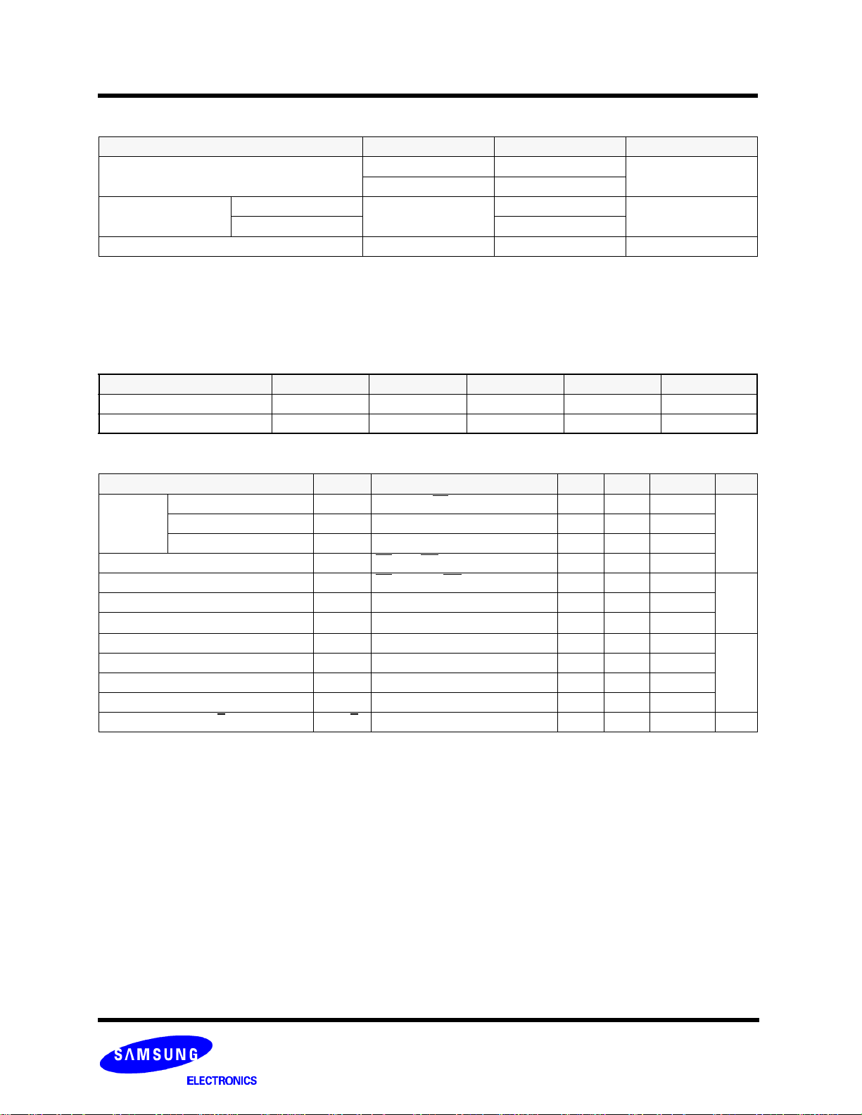
1. Changed DC characteristics
Parameter Min Typ Max Unit
Operating
Current
Sequential Read - 10 20->30
mAProgram - 10 20->30
Erase - 10 20->30
Draft Date
Oct. 27th 2000
Dec. 5th 2000
Dec. 15th 2000
Jan. 8th 2001
Apr. 7th 2001
Remark
Advanced
Information
2. Unified access timing parameter definition for multiple operating modes
- Changed AC characteristics (Before)
Parameter Symbol Min Max Unit
ALE to RE Delay( ID read ) tAR1 100 CE to RE Delay( ID read) tCR 100 RE Low to Status Output tRSTO - 35
CE Low to Status Output tCSTO - 45
RE access time(Read ID) tREADID - 35
ns
- AC characteristics (After)
. Deleted tCR,tRSTO, tCSTO and tREADID / Added tCEA
Parameter Symbol Min Max Unit
ALE to RE Delay( ID read ) tAR1 10 CE Access Time tCEA - 45
1
ns
K9F1208U0M-YCB0, K9F1208U0M-YIB0 FLASH MEMORY
Revision History
Revision No RemarkHistory Draft Date
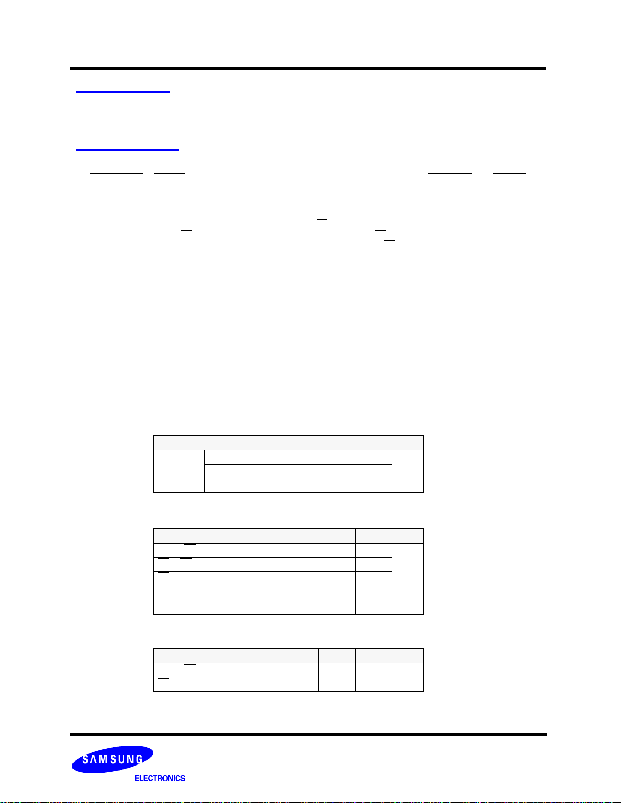
CLE
CE
WE
ALE
RE
I/O0~
CLE
CE
WE
ALE
RE
I/O0~
CLE
CE
WE
RE
I/O0~
tCR
tAR1
tWHR
tCLS
tWHR
tAR1
tIR
tREA
tCEA
tCSTO
tREA
tRSTO
ECh
Maker code
ECh
Maker code
tCHZ*
tRHZ*
Status Output
7
7
7
90h
90h
tCLS
Address. 1cycle
Address. 1cycle
tCS
tWP
tDS
00h
00h
tCLH
tCH
tDH
70h
CLE
CE
WE
RE
I/O0~
tCLS
tCS
tWP
tDS
7
70h
tCLH
tCH
tDH
tCLS
tWHR
tCEA
tREA
tIR
tCHZ*
tRHZ*
Status Output
The attached data sheets are prepared and approved by SAMSUNG Electronics. SAMSUNG Electronics CO., LTD. reserve the
right to change the specifications. SAMSUNG Electronics will evaluate and reply to your requests and questions about device. If you
have any questions, please contact the SAMSUNG branch office near your office.
2
K9F1208U0M-YCB0, K9F1208U0M-YIB0 FLASH MEMORY
≈
Revision No
0.5
0.6
0.7
History
1. Addition of new operation : Multi-Plane Copy-Back Program.
- Multi-Plane Copy-Back Program is extended operation of one-page
Copy-Back program.
=> After successive reading of multiple 528 byte data set at the source
planes, the above data are moved to internal page registers and same
procedure as Multi-Plane Page Programming is executed.
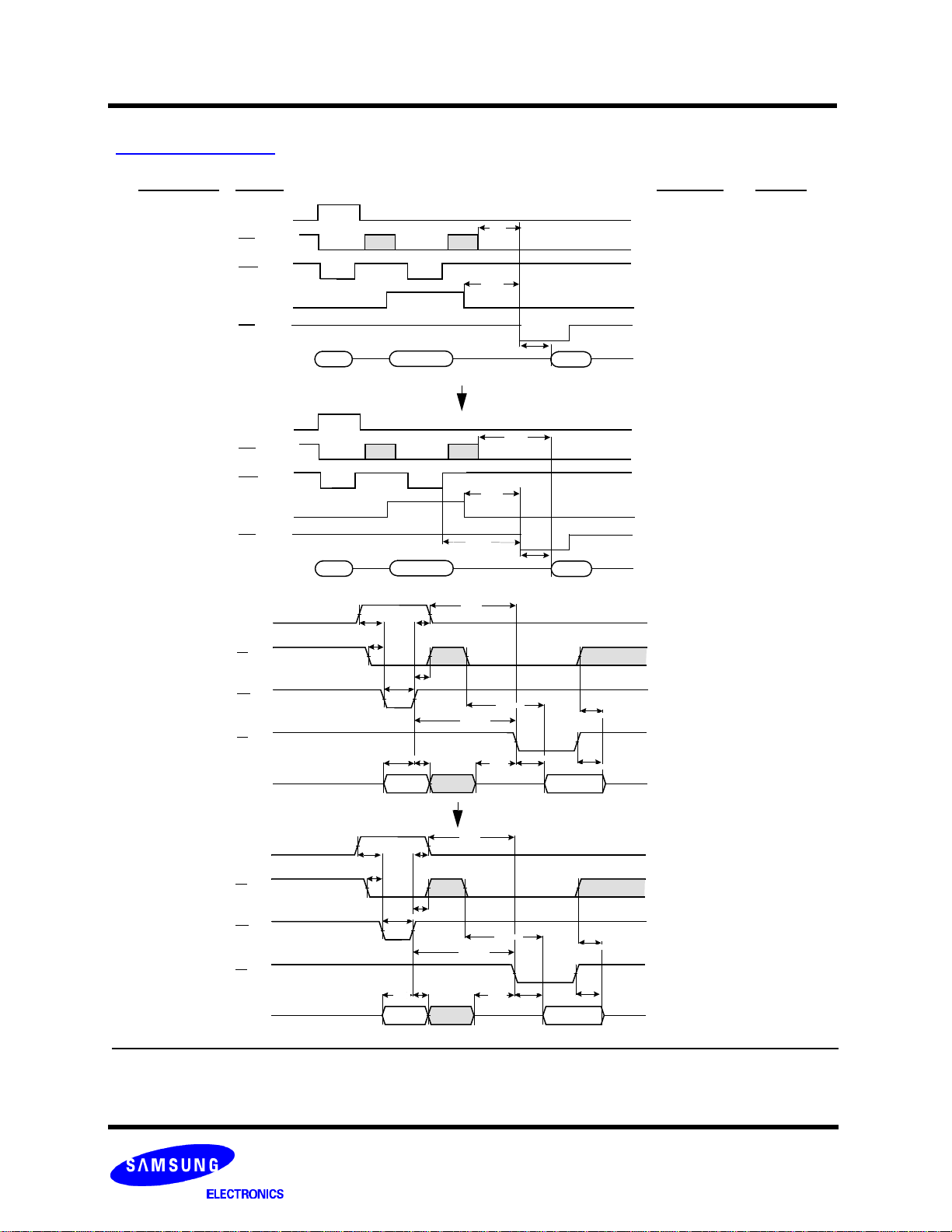
1.Powerup sequence is added
: Recovery time of minimum 1µs is required before internal circuit gets
ready for any command sequences
~ 2.5V
V
CC
High
WP
WE
1µs
≈
≈
~ 2.5V
2. AC parameter tCLR(CLE to RE Delay, min 50ns) is added.
1. Copy-Back Program(Dummy) is added in Command sets table.
(before revision)
Function
1st.
Cycle
Page Program (True) 80h 10h Page Program (Dummy) 80h 11h Copy-Back Program(True) 00h 8Ah 10h
2nd.
Cycle
3rd.
Cycle
Draft Date
May. 30th 2001
Jul. 23th 2001
Aug. 23th 2001
Remark
Preliminary
(after revision)
Function
Page Program (True)
Page Program (Dummy)
Copy-Back Program(True)
Copy-Back Program(Dummy)
Note 2. Page Program(True) and Copy-Back Program(True) are available on 1 plane
operation.
Page Program(Dummy) and Copy-Back Program(Dummy) are available on
the 2nd,3rd,4th plane of multi plane operation.
(2)
(2)
(2)
(2)
1st.
Cycle
80h 10h 80h 11h 00h 8Ah 10h
03h 8Ah 11h/10h
3
2nd.
Cycle
3rd.
Cycle

K9F1208U0M-YCB0, K9F1208U0M-YIB0 FLASH MEMORY
Revision No
0.8
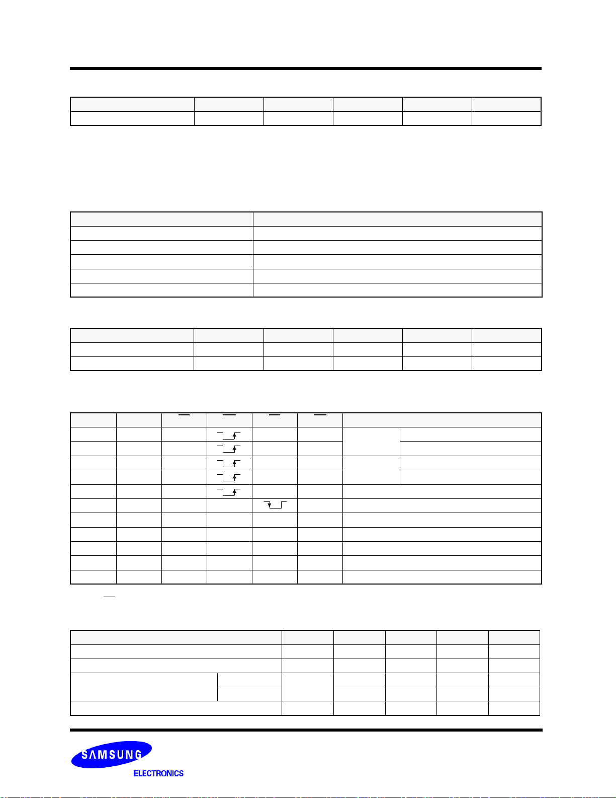
1. In Read ID & Status Read timing diagram, tCLS is changed to tCLR.
00h
Address. 1cycle
00h
Address. 1cycle
tCLS
tCLR
tWHR
tWHR
tAR1
tAR1
tCEA
tREA
tCEA
tREA
ECh
Maker code
Maker code
ECh
CLE
CE
WE
ALE
RE
I/O0~
CLE
CE
WE
ALE
RE
I/O0~
7
7
90h
90h
Draft Date
Oct. 7th 2001
RemarkHistory
CLE
CE
WE
RE
I/O0~
CLE
CE
WE
RE
I/O0~
tCLS
tCS
tWP
tDS
7
7
70h
tCLS
tCS
tWP
tDS
70h
tCLH
tCH
tDH
tCLH
tCH
tDH
tCLS
tWHR
tCLR
tWHR
tCEA
tREA
tIR
tCEA
tREA
tIR
tCHZ*
tRHZ*
Status Output
tCHZ*
tRHZ*
Status Output
4

K9F1208U0M-YCB0, K9F1208U0M-YIB0 FLASH MEMORY
Revision No
0.9
To clarify the meaning of parameter,
1. tRHZ is devide into tRHZ and tOH.(page 12)
- tRHZ : RE High to Output Hi-Z
- tOH : RE High to Output Hold
2. tCHZ is devide into tCHZ and tOH.(page 12)
- tCHZ : CE High to Output Hi-Z
- tOH : CE High to Output Hold
Draft Date
Apr. 20th 2002
RemarkHistory
5
K9F1208U0M-YCB0, K9F1208U0M-YIB0 FLASH MEMORY
64M x 8 Bit NAND Flash Memory
General DescriptionFeatures
• Voltage Supply : 2.7V~3.6V
• Organization
- Memory Cell Array : (64M + 2,048K)bit x 8bit
- Data Register : (512 + 16)bit x8bit multipled by four planes
• Automatic Program and Erase
- Page Program : (512 + 16)Byte
- Block Erase : (16K + 512)Byte
• 528-Byte Page Read Operation
- Random Access : 12µs(Max.)
- Serial Page Access : 50ns(Min.)
• Fast Write Cycle Time
- Program time : 200µs(Typ.)
- Block Erase Time : 2ms(Typ.)
• Command/Address/Data Multiplexed I/O Port
• Hardware Data Protection
- Program/Erase Lockout During Power Transitions
• Reliable CMOS Floating-Gate Technology
- Endurance : 100K Program/Erase Cycles
- Data Retention : 10 Years
• Command Register Operation
• Intelligent Copy-Back Operation
• Package :
- K9F1208U0M-YCB0, K9F1208U0M-YIB0 :
48 - Pin TSOP I (12 x 20 / 0.5 mm pitch)
• Simultaneous Four Page/Block Program/Erase
The K9F1208U0M is a 64M(67,108,864)x8bit NAND Flash
Memory with a spare 2,048K(2,097,152)x8bit. Its NAND cell
provides the most cost-effective solution for the solid state
mass storage market. A program operation can be performed in
typical 200µs on the 528-byte page and an erase operation can
be performed in typical 2ms on a 16K-byte block. Data in the
page can be read out at 50ns cycle time per byte. The I/O pins
serve as the ports for address and data input/output as well as
command inputs. The on-chip write controller automates all
program and erase functions including pulse repetition, where
required, and internal verification and margining of data. Even
the write-intensive systems can take advantage of the
K9F1208U0M’s extended reliability of 100K program/erase
cycles by providing ECC(Error Correcting Code) with real time
mapping-out algorithm. The K9F1208U0M-YCB0/YIB0 is an
optimum solution for large nonvolatile storage applications such
as solid state file storage and other portable applications requiring non-volatility.
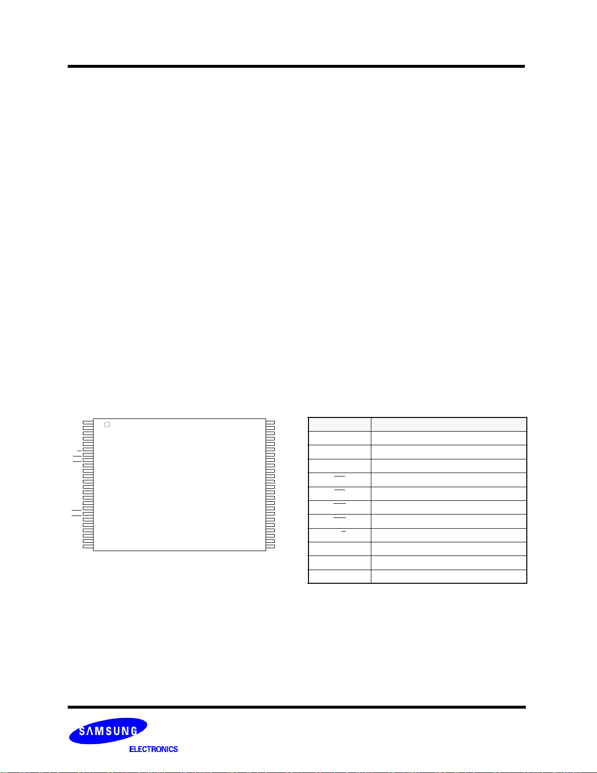
Pin Configuration
N.C
1
N.C
2
N.C
3
N.C
4
N.C
5
N.C
6
R/B
7
RE
8
CE
9
N.C
10
N.C
11
Vcc
12
Vss
13
N.C
14
N.C
15
CLE
16
ALE
17
WE
18
WP
19
N.C
20
N.C
21
N.C
22
23
N.C
24
N.C
48-pin TSOP1
Standard Type
12mm x 20mm
N.C
48
N.C
47
N.C
46
N.C
45
I/O7
44
I/O6
43
I/O5
42
I/O4
41
N.C
40
N.C
39
N.C
38
Vcc
37
Vss
36
N.C
35
N.C
34
N.C
33
I/O3
32
I/O2
31
I/O1
30
I/O0
29
N.C
28
N.C
27
N.C
26
N.C
25
Pin Description
Pin Name Pin Function
I/O0 ~ I/O7 Data Input/Outputs
CLE Command Latch Enable
ALE Address Latch Enable
CE Chip Enable
RE Read Enable
WE Write Enable
WP Write Protect
R/B Ready/Busy output
VCC Power(+2.7V~3.6V)
VSS Ground
N.C No Connection
NOTE : Connect all VCC and VSS pins of each device to common power supply outputs.
Do not leave VCC or VSS disconnected.
6
K9F1208U0M-YCB0, K9F1208U0M-YIB0 FLASH MEMORY
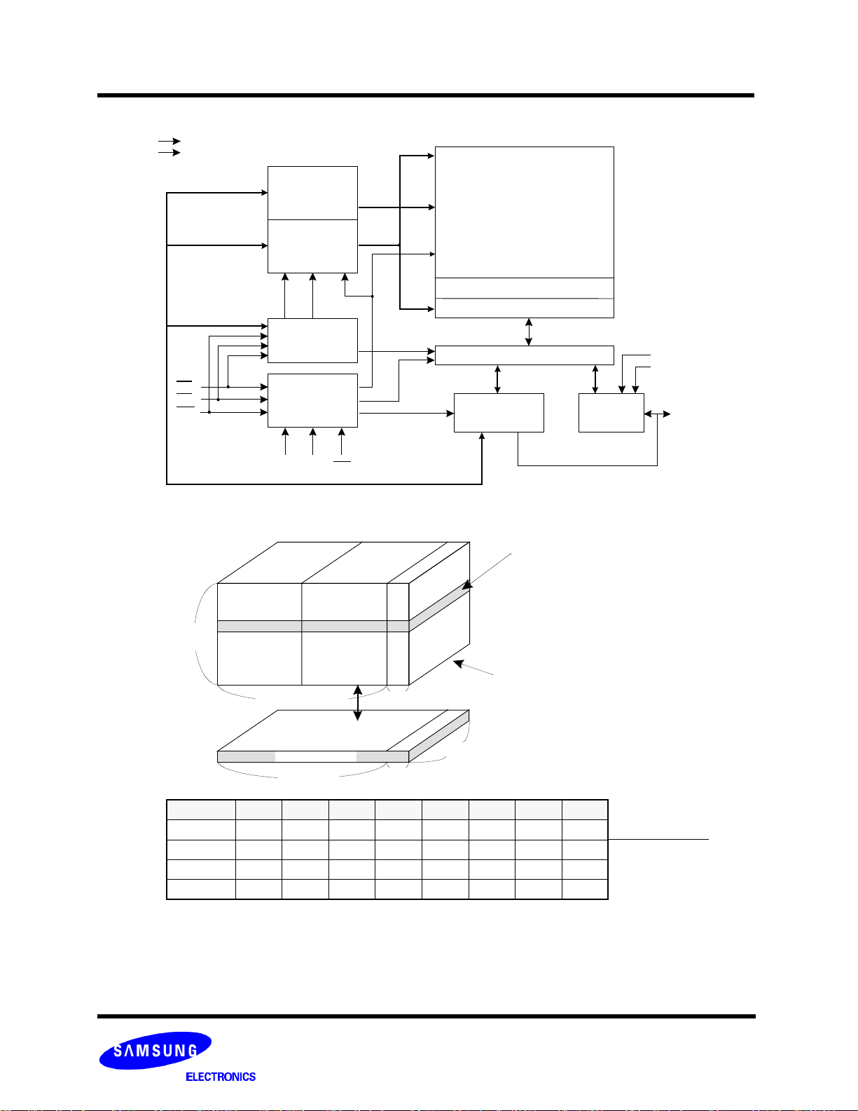
Figure 1. Functional Block Diagram
VCC
VSS
A9 - A25
X-Buffers
Latches
& Decoders
A0 - A7
Y-Buffers
Latches
& Decoders
Command
Command
Register
CE
RE
WE
Control Logic
& High Voltage
Generator
CLE
Figure 2. Array Organization
ALE
A8
WP
512M + 16M Bit
NAND Flash
ARRAY
(512 + 16)Byte x 131072
Page Register & S/A
Y-Gating
I/O Buffers & Latches
Global Buffers
1 Block = 32 Pages
(16K + 512) Byte
Output
Driver
VCC
VSS
I/0 0
I/0 7
128K Pages
(=4,096 Blocks)
1st half Page Register
(=256 Bytes)
2nd half Page Register
(=256 Bytes)
512B Bytes 16 Bytes
Page Register
512 Bytes
I/O 0 I/O 1 I/O 2 I/O 3 I/O 4 I/O 5 I/O 6 I/O 7
1st Cycle A0 A1 A2 A3 A4 A5 A6 A7
2nd Cycle A9 A10 A11 A12 A13 A14 A15 A16
3rd Cycle A17 A18 A19 A20 A21 A22 A23 A24
4th Cycle A25 *L *L *L *L *L *L *L
NOTE : Column Address : Starting Address of the Register.
00h Command(Read) : Defines the starting address of the 1st half of the register.
01h Command(Read) : Defines the starting address of the 2nd half of the register.
* A8 is set to "Low" or "High" by the 00h or 01h Command.
* L must be set to "Low".
* The device ignores any additional input of address cycles than reguired.
1 Page = 528 Bytes
1 Block = 528 B x 32 Pages
= (16K + 512) Bytes
1 Device = 528B x 32Pages x 4,096 Blocks
= 528 Mbits
8 bit
I/O 0 ~ I/O 7
16 Bytes
Column Address
Row Address
(Page Address)
7
K9F1208U0M-YCB0, K9F1208U0M-YIB0 FLASH MEMORY
Product Introduction
The K9F1208U0M is a 528Mbit(553,648,218 bit) memory organized as 131,072 rows(pages) by 528 columns. Spare sixteen columns
are located from column address of 512 to 527. A 528-byte data register is connected to memory cell arrays accommodating data
transfer between the I/O buffers and memory during page read and page program operations. The memory array is made up of 16
cells that are serially connected to form a NAND structure. Each of the 16 cells resides in a different page. A block consists of the 32
pages formed by two NAND structures, totaling 8,192 NAND structures of 16 cells. The array organization is shown in Figure 2. The
program and read operations are executed on a page basis, while the erase operation is executed on a block basis. The memory
array consists of 4,096 separately erasable 16K-byte blocks. It indicates that the bit by bit erase operation is prohibited on the
K9F1208U0M.
The K9F1208U0M has addresses multiplexed into 8 I/O's. This scheme dramatically reduces pin counts and allows systems
upgrades to future densities by maintaining consistency in system board design. Command, address and data are all written through
I/O's by bringing WE to low while CE is low. Data is latched on the rising edge of WE. Command Latch Enable(CLE) and Address
Latch Enable(ALE) are used to multiplex command and address respectively, via the I/O pins. The 64M byte physical space requires
26 addresses, thereby requiring four cycles for byte-level addressing: column address, low row address and high row address, in that
order. Page Read and Page Program need the same four address cycles following the required command input. In Block Erase operation, however, only the three row address cycles are used. Device operations are selected by writing specific commands into the
command register. Table 1 defines the specific commands of the K9F1208U0M.
The device provides simultaneous program/erase capability up to four pages/blocks. By dividing the memory array into four 128Mbit
separate planes, simultaneous multi-plane operation dramatically increases program/erase performance by 4X while still maintaining
the conventional 512 byte structure.
The extended pass/fail status for multi-plane program/erase allows system software to quickly identify the failing page/block out of
selected multiple pages/blocks. Usage of multi-plane operations will be described further throughout this document.
In addition to the enhanced architecture and interface, the device incorporates copy-back program feature from one page to another
of the same plane without the need for transporting the data to and from the external buffer memory. Since the time-consuming burstreading and data-input cycles are removed, system performance for solid-state disk application is significantly increased.
Table 1. Command Sets
Function 1st. Cycle 2nd. Cycle 3rd. Cycle
Read 1
00h/01h
(1)
- Read 2 50h - Read ID 90h - Reset FFh - - O
Page Program (True)
Page Program (Dummy)
Copy-Back Program(True)
(2)
(2)
(2)
Copy-Back Program(Dummy)
(2)
80h 10h 80h 11h 00h 8Ah 10h
03h 8Ah 11h
Block Erase 60h D0h Multi-Plane Block Erase 60h----60h D0h Read Status 70h - - O
Read Multi-Plane Status
NOTE : 1. The 00h command defines starting address of the 1st half of registers.
The 01h command defines starting address of the 2nd half of registers.
After data access on the 2nd half of register by the 01h command, the status pointer is
automatically moved to the 1st half register(00h) on the next cycle.
2. Page Program(True) and Copy-Back Program(True) are available on 1 plane operation.
Page Program(Dummy) and Copy-Back Program(Dummy) are available on the 2nd,3rd,4th plane of multi plane operation.
3. The 71h command should be used for read status of Multi Plane operation.
71h
(3)
- - O
Acceptable Command
during Busy
Caution : Any undefined command inputs are prohibited except for above command set of Table 1.
8
K9F1208U0M-YCB0, K9F1208U0M-YIB0 FLASH MEMORY
Memory Map
The device is arranged in four 128Mbit memory planes. Each plane contains 1,024 blocks and 528 byte page registers. This allows it
to perform simultaneous page program and block erase by selecting one page or block from each plane. The block address map is
configured so that multi-plane program/erase operations can be executed for every four sequential blocks.
Figure 3. Memory Array Map
Plane 0
(1024 Block)
Block 0
Page 0
Page 1
Page 30
Page 31
Block 4
Page 0
Page 1
Page 30
Page 31
Block 4088
Page 0
Page 1
Plane 1
(1024 Block)
Block 1
Page 0
Page 1
Page 30
Page 31
Block 5
Page 0
Page 1
Page 30
Page 31
Block 4089
Page 0
Page 1
Plane 2
(1024 Block)
Block 2
Page 0
Page 1
Page 30
Page 31
Block 6
Page 0
Page 1
Page 30
Page 31
Block 4090
Page 0
Page 1
Plane 3
(1024 Block)
Block 3
Page 0
Page 1
Page 30
Page 31
Block 7
Page 0
Page 1
Page 30
Page 31
Block 4091
Page 0
Page 1
Page 30
Page 31
Block 4092
Page 0
Page 1
Page 30
Page 31
528byte Page Registers
Page 30
Page 31
Block 4093
Page 0
Page 1
Page 30
Page 31
528byte Page Registers 528byte Page Registers 528byte Page Registers
Page 30
Page 31
Block 4094
Page 0
Page 1
Page 30
Page 31
Page 30
Page 31
Block 4095
Page 0
Page 1
Page 30
Page 31
9
K9F1208U0M-YCB0, K9F1208U0M-YIB0 FLASH MEMORY
Pin Description
Command Latch Enable(CLE)
The CLE input controls the path activation for commands sent to the command register. When active high, commands are latched
into the command register through the I/O ports on the rising edge of the WE signal.
Address Latch Enable(ALE)
The ALE input controls the activating path for address to the internal address registers. Addresses are latched on the rising edge of
WE with ALE high.
Chip Enable(CE)
The CE input is the device selection control. When CE goes high during a read operation the device is returned to standby mode.
However, when the device is in the busy state during program or erase, CE high is ignored, and does not return to the standby mode.
Write Enable(WE)
The WE input controls writes to the I/O port. Commands, address and data are latched on the rising edge of the WE pulse.
The WE must be held high when outputs are activated.
Read Enable(RE)
The RE input is the serial data-out control, and when active drives the data onto the I/O bus. Data is valid tREA after the falling edge
of RE which also increments the internal column address counter by one.
I/O Port : I/O 0 ~ I/O 7
The I/O pins are used to input command, address and data, and to output data during read operations. The I/O pins float to high-z
when the chip is deselected or when the outputs are disabled.
Write Protect(WP)
The WP pin provides inadvertent write/erase protection during power transitions. The internal high voltage generator is reset when
the WP pin is active low.
Ready/Busy(R/B)
The R/B output indicates the status of the device operation. When low, it indicates that a program, erase or random read operation is
in process and returns to high state upon completion. It is an open drain output and does not float to high-z condition when the chip
is deselected or when outputs are disabled.
10
K9F1208U0M-YCB0, K9F1208U0M-YIB0 FLASH MEMORY
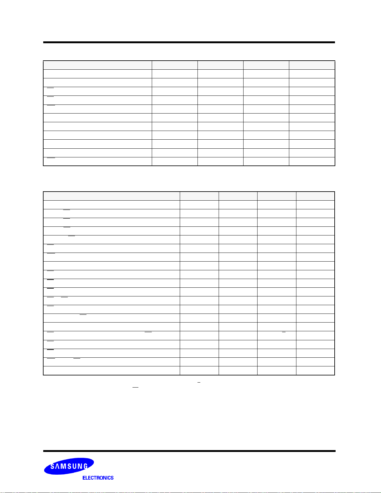
Absolute Maximum Ratings
Parameter Symbol Rating Unit
Voltage on any pin relative to VSS
Temperature Under Bias
Storage Temperature TSTG -65 to +150 °C
NOTE :
1. Minimum DC voltage is -0.6V on input/output pins. During transitions, this level may undershoot to -2.0V for periods <30ns.
Maximum DC voltage on input/output pins is VCC,+0.3V which, during transitions, may overshoot to VCC+2.0V for periods <20ns.
2. Permanent device damage may occur if ABSOLUTE MAXIMUM RATINGS are exceeded. Functional operation should be restricted to the conditions
as detailed in the operational sections of this data sheet. Exposure to absolute maximum rating conditions for extended periods may affect reliability.
K9F1208U0M-YCB0
K9F1208U0M-YIB0 -40 to +125
Recommended Operating Conditions
(Voltage reference to GND, K9F1208U0M-YCB0 :TA=0 to 70°C, K9F1208U0M-YIB0:TA=-40 to 85°C)
Parameter Symbol Min Typ. Max Unit
Supply Voltage VCC 2.7 3.3 3.6 V
Supply Voltage VSS 0 0 0 V
Dc and Operating Characteristics(Recommended operating conditions otherwise noted.)
Parameter Symbol Test Conditions
Operating
Current
Stand-by Current(TTL) ISB1 CE=VIH, WP= 0V/VCC - - 1
Stand-by Current(CMOS) ISB2 CE=VCC-0.2, WP = 0V/VCC - 10 50
Input Leakage Current ILI VIN=0 to 3.6V - - ±10
Output Leakage Current ILO VOUT=0 to 3.6V - - ±10
Input High Voltage VIH - 2.0 - VCC+0.3
Input Low Voltage, All inputs VIL - -0.3 - 0.8
Output High Voltage Level VOH IOH=-400µA 2.4 - Output Low Voltage Level
Output Low Current(R/B) IOL(R/B) VOL=0.4V 8 10 - mA
Sequential Read ICC1 tRC=50ns, CE=VIL, IOUT=0mA - 10 30
Program ICC2 - - 10 30
Erase ICC3 - - 10 30
VOL IOL=2.1mA - - 0.4
VIN -0.6 to + 4.6
VCC -0.6 to + 4.6
TBIAS
-10 to +125
Min
Typ
Max
V
°C
Unit
mA
µA
V
11
K9F1208U0M-YCB0, K9F1208U0M-YIB0 FLASH MEMORY
Valid Block
Parameter Symbol Min Typ. Max Unit
Valid Block Number NVB 4,026 - 4,096 Blocks
NOTE :
1. The K9F1208U0M may include invalid blocks when first shipped. Additional invalid blocks may develop while being used. The number of valid
blocks is presented with both cases of invalid blocks considered. Invalid blocks are defined as blocks that contain one or more bad bits. Do not erase
or program factory-marked bad blocks. Refer to the attached technical notes for an appropriate management of invalid blocks.
2. The 1st block, which is placed on 00h block address, is fully guaranteed to be a valid block, does not require Error Correction.
AC Test Condition
(K9F1208U0M-YCB0 :TA=0 to 70°C, K9F1208U0M-YIB0:TA=-40 to 85°C, VCC=2.7V~3.6V unless otherwise)
Parameter Value
Input Pulse Levels 0.4V to 2.4V
Input Rise and Fall Times
Input and Output Timing Levels 1.5V
Output Load (3.0V +/-10%) 1 TTL GATE and CL=50pF
Output Load (3.3V +/-10%) 1 TTL GATE and CL=100pF
Capacitance(TA=25°C, VCC=3.3V, f=1.0MHz)
Item Symbol Test Condition Min Max Unit
Input/Output Capacitance CI/O VIL=0V - 10 pF
Input Capacitance CIN VIN=0V - 10 pF
NOTE : Capacitance is periodically sampled and not 100% tested.
5ns
MODE SELECTION
CLE ALE CE WE RE WP Mode
H L L H X
L H L H X Address Input(4clock)
H L L H H
L H L H H Address Input(4clock)
L L L H H Data Input
L L L H X Sequential Read & Data Output
L L L H H X During Read(Busy)
X X X X X H During Program(Busy)
X X X X X H During Erase(Busy)
X
X X H X X
NOTE : 1. X can be VIL or VIH.
2. WP should be biased to CMOS high or CMOS low for standby.
(1)
X
X X X L Write Protect
0V/VCC
(2)
Read Mode
Write Mode
Stand-by
Command Input
Command Input
Program / Erase Characteristics
Parameter Symbol Min Typ Max Unit
Program Time tPROG - 200 500 µs
Dummy Busy Time for Multi Plane Program tDBSY 1 10 µs
Number of Partial Program Cycles
in the Same Page
Block Erase Time tBERS - 2 3 ms
Main Array
Spare Array - - 2 cycles
Nop
- - 1 cycle
12
K9F1208U0M-YCB0, K9F1208U0M-YIB0 FLASH MEMORY
AC Timing Characteristics for Command / Address / Data Input
Parameter Symbol Min Max Unit
CLE setup Time tCLS 0 - ns
CLE Hold Time tCLH 10 - ns
CE setup Time tCS 0 - ns
CE Hold Time
WE Pulse Width tWP
ALE setup Time tALS 0 - ns
ALE Hold Time
Data setup Time tDS 20 - ns
Data Hold Time tDH 10 - ns
Write Cycle Time tWC 50 - ns
WE High Hold Time
NOTE : 1. If tCS is set less than 10ns, tWP must be minimum 35ns, otherwise, tWP may be minimum 25ns.
AC Characteristics for Operation
Parameter Symbol Min Max Unit
Data Transfer from Cell to Register tR - 12 µs
ALE to RE Delay( ID read ) tAR1 10 - ns
ALE to RE Delay(Read cycle) tAR2 50 - ns
CLE to RE Delay tCLR 50 - ns
Ready to RE Low tRR 20 - ns
RE Pulse Width tRP 30 - ns
WE High to Busy tWB - 100 ns
Read Cycle Time tRC 50 - ns
RE Access Time tREA - 35 ns
RE High to Output Hi-Z tRHZ - 30 ns
CE High to Output Hi-Z
RE or CE High to Output hold tOH 15 - ns
RE High Hold Time tREH 15 - ns
Output Hi-Z to RE Low tIR 0 - ns
Last RE High to Busy(at sequential read) tRB - 100 ns
CE High to Ready(in case of interception by CE at read) tCRY CE High Hold Time(at the last serial read)
CE Access Time tCEA - 45 ns
WE High to RE Low tWHR 60 - ns
Device Resetting Time(Read/Program/Erase) tRST -
NOTE :
1. The time to Ready depends on the value of the pull-up resistor tied R/B pin.
2. To break the sequential read cycle, CE must be held high for longer time than tCEH.
3. If reset command(FFh) is written at Ready state, the device goes into Busy for maximum 5us.
(2)
tCH 10 - ns
(1)
25
tALH 10 -
- ns
ns
tWH 15 - ns
tCHZ - 20 ns
50 +tr(R/B)
(1)
tCEH 100 - ns
5/10/500
(3)
ns
µs
13
 Loading...