

Samsung K6T4008U1C-TB10, K6T4008U1C-MF85, K6T4008U1C-MB85, K6T4008U1C-MB70, K6T4008U1C-MB10 Datasheet
...
K6T4008V1C, K6T4008U1C Family
Document Title
512Kx8 bit Low Power and Low Voltage CMOS Static RAM
Revision History
CMOS SRAM
Revision No.
0.0
0.1
0.11
1.0
History
Initial Draft
Revisied
- Speed bin change
KM68U4000C : 85/100ns → 70/85/100ns
- DC Characteristics change
ICC : 5mA at read/write → 4mA at read
ICC1 : 3mA → 4mA
ICC2 : 35mA → 30mA
ISB : 0.5mA → 0.3mA
ISB1 : 10µA → 15µA for commercial parts
- Add 32-TSOP1-0820
Errata correct
- 32-TSOP1-0813 products: T → TG
Finalize
Draft Data
January 13, 1998
June 12, 1998
November 7, 1998
January 15, 1999
Remark
Advance
Preliminary
Final
The attached datasheets are provided by SAMSUNG Electronics. SAMSUNG Electronics CO., LTD. reserve the right to change the specifications and
products. SAMSUNG Electronics will answer to your questions about device. If you have any questions, please contact the SAMSUNG branch offices.
1
Revision 1.0
January 1999
K6T4008V1C, K6T4008U1C Family
512K×8 bit Low Power and Low Voltage CMOS Static RAM
CMOS SRAM
FEATURES
• Process Technology: TFT
• Organization: 512K×8
• Power Supply Voltage
K6T4008V1C Family: 3.0~3.6V
K6T4008U1C Family: 2.7~3.3V
• Low Data Retention Voltage: 2V(Min)
• Three state output and TTL Compatible
• Package Type: 32-SOP-525, 32-TSOP2-400F/R
32-TSOP1-0820F, 32-TSOP1-0813.4F
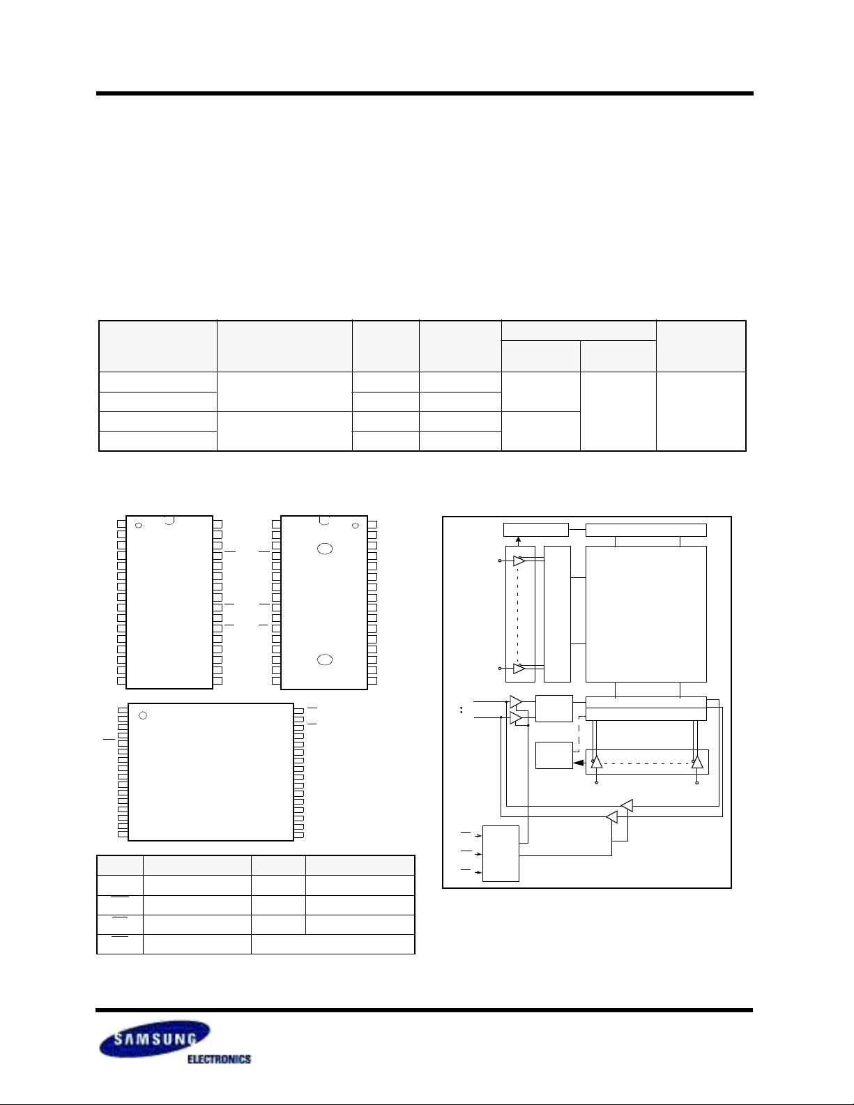
PRODUCT FAMILY
Product Family Operating Temperature Vcc Range Speed
K6T4008V1C-B
K6T4008U1C-B 2.7~3.3V
K6T4008V1C-F
K6T4008U1C-F 2.7~3.3V
Commercial(0~70°C)
Industrial(-40~85°C)
1. The paramerter is measured with 30pF test load.
3.0~3.6V
701)/85/100ns
3.0~3.6V
701)/85/100ns
PIN DESCRIPTION
A18
1
2
A16
A14
3
A12
4
5
A7
A6
6
A5
7
8
32-TSOP2
9
(Forward)
10
11
12
13
14
15
16
1
2
3
4
5
6
7
8
9
10
11
12
13
14
15
16
32-SOP
I/O1
I/O2
I/O3
VSS
A11
A13
A17
A15
VCC
A18
A16
A14
A12
A4
A3
A2
A1
A0
A9
A8
WE
A7
A6
A5
A4
Name Function Name Function
A0~A18 Address Inputs Vcc Power
WE Write Enable Input Vss Ground
CS Chip Select Input I/O1~I/O8 Data Inputs/Outputs
OE Output Enable Input
VCC
32
A15
31
A17
30
WE
29
A13
28
A8
27
A9
26
A11
25
24
OE
23
A10
22
CS
21
I/O8
20
I/O7
19
I/O6
18
I/O5
17
I/O4
32-TSOP1
32-STSOP1
(Forward)
VCC
A15
A17
WE
A13
A11
OE
A10
CS
I/O8
I/O7
I/O6
I/O5
I/O4
32
31
30
29
28
A8
27
A9
26
32-TSOP2
25
(Reverse)
24
23
22
21
20
19
18
17
32
OE
A10
31
30
CS
I/O8
29
28
I/O7
27
I/O6
26
I/O5
25
I/O4
24
VSS
23
I/O3
22
I/O2
21
I/O1
20
A0
19
A1
18
A2
17
A3
1
A18
2
A16
A14
3
A12
4
5
A7
A6
6
A5
7
A4
8
A3
9
A2
10
A1
11
A0
12
I/O1
13
I/O2
14
I/O3
15
VSS
16
GENERAL DESCRIPTION
The K6T4008V1C and K6T4008U1C families are fabricated by
SAMSUNG′s advanced CMOS process technology. The families support various operating temperature range and have various package type for user flexibility of system design. The
families also support low data retention voltage for battery
back-up operation with low data retention current.
Power Dissipation
PKG Type
32-SOP
32-TSOP2-F/R
32-TSOP1-F
32-sTSOP1-F
701)/85ns
701)/85ns
Standby
(ISB1, Max)
15µA
20µA
Operating
(ICC2, Max)
30mA
FUNCTIONAL BLOCK DIAGRAM
Clk gen.
A0
A1
A4
A5
A6
A7
A12
A14
A16
A18
I/O1 Data
I/O8
CS
Control
WE
logic
OE
Row
select
cont
Data
cont
Precharge circuit.
Memory array
1024 rows
512×8 columns
I/O Circuit
Column select
A2 A3 A8 A9 A10 A13A11
A15
A17
SAMSUNG ELECTRONICS CO., LTD. reserves the right to change products and specifications without notice.
2
Revision 1.0
January 1999
K6T4008V1C, K6T4008U1C Family
PRODUCT LIST
Commercial Temp Products(0~70°C) Industrial Temp Products(-40~85°C)
Part Name Function Part Name Function
K6T4008V1C-GB70
K6T4008V1C-GB85
K6T4008V1C-VB70
K6T4008V1C-VB85
K6T4008V1C-MB70
K6T4008V1C-MB85
K6T4008V1C-TB70
K6T4008V1C-TB85
K6T4008V1C-YB70
K6T4008V1C-YB85
32-SOP, 70ns, 3.3V, LL
32-SOP, 85ns, 3.3V, LL
32-TSOP2-F, 70ns, 3.3V, LL
32-TSOP2-F, 85ns, 3.3V, LL
32-TSOP2-R, 70ns, 3.3V, LL
32-TSOP2-R, 85ns, 3.3V, LL
32-TSOP1-F, 70ns, 3.3V, LL
32-TSOP1-F, 85ns, 3.3V, LL
32-sTSOP1-F, 70ns, 3.3V, LL
32-sTSOP1-F, 85ns, 3.3V, LL
K6T4008V1C-GF70
K6T4008V1C-GF85
K6T4008V1C-VF70
K6T4008V1C-VF85
K6T4008V1C-MF70
K6T4008V1C-MF85
K6T4008V1C-TF70
K6T4008V1C-TF85
K6T4008V1C-YF70
K6T4008V1C-YF85
CMOS SRAM
32-SOP, 70ns, 3.3V, LL
32-SOP, 85ns, 3.3V, LL
32-TSOP2-F, 70ns, 3.3V, LL
32-TSOP2-F, 85ns, 3.3V, LL
32-TSOP2-R, 70ns, 3.3V, LL
32-TSOP2-R, 85ns, 3.3V, LL
32-TSOP1-F, 70ns, 3.3V, LL
32-TSOP1-F, 85ns, 3.3V, LL
32-sTSOP1-F, 70ns, 3.3V, LL
32-sTSOP1-F, 85ns, 3.3V, LL
K6T4008U1C-GB70
K6T4008U1C-GB85
K6T4008U1C-GB10
K6T4008U1C-VB70
K6T4008U1C-VB85
K6T4008U1C-VB10
K6T4008U1C-MB70
K6T4008U1C-MB85
K6T4008U1C-MB10
K6T4008U1C-TB70
K6T4008U1C-TB85
K6T4008U1C-TB10
K6T4008U1C-YB70
K6T4008U1C-YB85
K6T4008U1C-YB10
32-SOP, 70ns, 3.0V, LL
32-SOP, 85ns, 3.0V, LL
32-SOP, 100ns, 3.0V, LL
32-TSOP2-F, 70ns, 3.0V, LL
32-TSOP2-F, 85ns, 3.0V, LL
32-TSOP2-F, 100ns, 3.0V, LL
32-TSOP2-R, 70ns, 3.0V, LL
32-TSOP2-R, 85ns, 3.0V, LL
32-TSOP2-R, 100ns, 3.0V, LL
32-TSOP1-F, 70ns, 3.0V, LL
32-TSOP1-F, 85ns, 3.0V, LL
32-TSOP1-F, 100ns, 3.0V, LL
32-sTSOP1-F, 70ns, 3.0V, LL
32-sTSOP1-F, 85ns, 3.0V, LL
32-sTSOP1-F, 100ns, 3.0V, LL
K6T4008U1C-GF70
K6T4008U1C-GF85
K6T4008U1C-GF10
K6T4008U1C-VF70
K6T4008U1C-VF85
K6T4008U1C-VF10
K6T4008U1C-MF70
K6T4008U1C-MF85
K6T4008U1C-MF10
K6T4008U1C-TF70
K6T4008U1C-TF85
K6T4008U1C-TF10
K6T4008U1C-YF70
K6T4008U1C-YF85
K6T4008U1C-YF10
32-SOP, 70ns, 3.0V, LL
32-SOP, 85ns, 3.0V, LL
32-SOP, 100ns, 3.0V, LL
32-TSOP2-F, 70ns, 3.0V, LL
32-TSOP2-F, 85ns, 3.0V, LL
32-TSOP2-F, 100ns, 3.0V, LL
32-TSOP2-R, 70ns, 3.0V, LL
32-TSOP2-R, 85ns, 3.0V, LL
32-TSOP2-R, 100ns, 3.0V, LL
32-TSOP1-F, 70ns, 3.0V, LL
32-TSOP1-F, 85ns, 3.0V, LL
32-TSOP1-F, 100ns, 3.0V, LL
32-sTSOP1-F, 70ns, 3.0V, LL
32-sTSOP1-F, 85ns, 3.0V, LL
32-sTSOP1-F, 100ns, 3.0V, LL
FUNCTIONAL DESCRIPTION
CS OE WE I/O Mode Power
H
L H H High-Z Output Disabled Active
L L H Dout Read Active
L
1. X means don′t care (Must be in low or high state)
1)
X
1)
X
1)
X
L Din Write Active
High-Z Deselected Standby
ABSOLUTE MAXIMUM RATINGS
Item Symbol Ratings Unit Remark
Voltage on any pin relative to Vss VIN,VOUT -0.5 to VCC+0.5 V Voltage on Vcc supply relative to Vss VCC -0.3 to 4.6 V Power Dissipation PD 1.0 W Storage temperature TSTG -65 to 150 °C -
Operating Temperature TA
1. Stresses greater than those listed under "Absolute Maximum Ratings" may cause permanent damage to the device. Functional operation should be
restricted to recommended operating condition. Exposure to absolute maximum rating conditions for extended periods may affect reliability.
1)
0 to 70 °C K6T4008V1C-L, K6T4008U1C-L
-40 to 85 °C K6T4008V1C-P, K6T4008U1C-P
3
Revision 1.0
January 1999
 Loading...