

SAMSUNG K4S640832K Technical data
K4S640832K
现货库存、技术资料、百科信息、热点资讯,精彩尽在鼎好!
K4S641632K
64Mb K-die SDRAM Specification
Synchronous DRAM
INFORMATION IN THIS DOCUMENT IS PROVIDED IN RELATION TO SAMSUNG PRODUCTS,
AND IS SUBJECT TO CHANGE WITHOUT NOTICE.
NOTHING IN THIS DOCUMENT SHALL BE CONSTRUED AS GRANTING ANY LICENSE,
EXPRESS OR IMPLIED, BY ESTOPPEL OR OTHERWISE,
TO ANY INTELLECTUAL PROPERTY RIGHTS IN SAMSUNG PRODUCTS OR TECHNOLOGY. ALL
INFORMATION IN THIS DOCUMENT IS PROVIDED
ON AS "AS IS" BASIS WITHOUT GUARANTEE OR WARRANTY OF ANY KIND.
1. For updates or additional information about Samsung products, contact your nearest Samsung office.
2. Samsung products are not intended for use in life support, critical care, medical, safety equipment, or similar
applications where Product failure couldresult in loss of life or personal or physical harm, or any military or
defense application, or any governmental procurement to which special terms or provisions may apply.
* Samsung Electronics reserves the right to change products or specification without notice.
1 of 14
Rev. 1.1 February 2006
K4S640832K
K4S641632K
Revision History
Revision Month Year History
0.0 January 2005 - Target spec release
0.1 March 2005 - Change DC current
0.2 April 2005 - Delete bit organization for x4
0.3 July 2005 - Delete 7ns speed bin
1.0 September 2005 - Final spec release
1.1 February 2006 - Added 5ns speed bin for x16
Synchronous DRAM
2 of 14
Rev. 1.1 February 2006
K4S640832K
K4S641632K
Synchronous DRAM
2M x 8Bit x 4Banks / 1M x 16Bit x 4Banks SDRAM
FEATURES
• JEDEC standard 3.3V power supply
• LVTTL compatible with multiplexed address
• Four banks operation
• MRS cycle with address key programs
-. CAS latency (2 & 3)
-. Burst length (1, 2, 4, 8 & Full page)
-. Burst type (Sequential & Interleave)
• All inputs are sampled at the positive going edge of the system clock
• Burst read single-bit write operation
• DQM (x8) & L(U)DQM (x16) for masking
• Auto & self refresh
• 64ms refresh period (4K cycle)
• Pb/Pb-free Package
• RoHS compliant for Pb-free Package
GENERAL DESCRIPTION
The K4S640832K / K4S641632K is 67,108,864 bits synchronous high data rate Dynamic RAM organized as 4 x 2,097,152 words by 8
bits, / 4 x 1,048,576 words by 16 bits, fabricated with SAMSUNG′s high performance CMOS technology. Synchronous design allows
precise cycle control with the use of system clock I/O transactions are possible on every clock cycle. Range of operating frequencies,
programmable burst length and programmable latencies allow the same device to be useful for a variety of high bandwidth, high performance memory system applications.
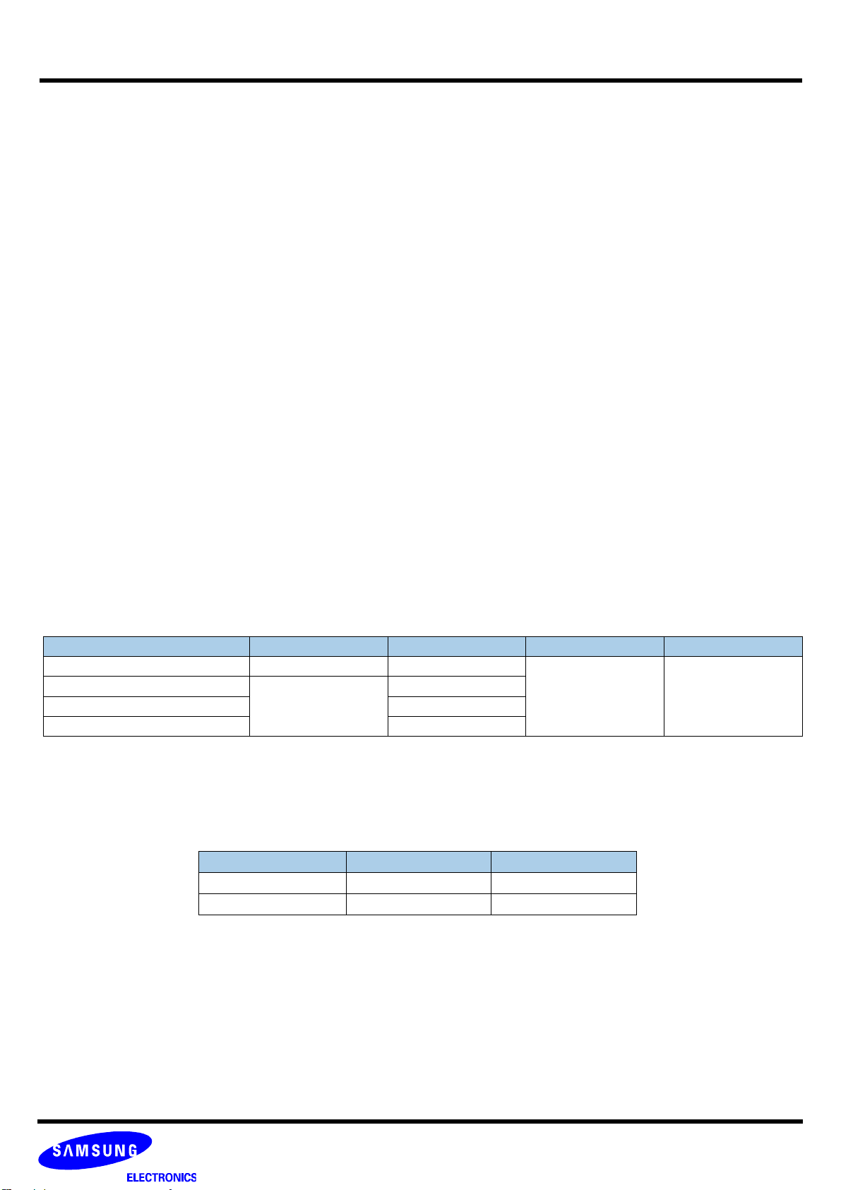
Ordering Information
Part No. Orgainization Max Freq. Interface Package
K4S640832K-T(U)C/L75 8Mb x 8 133MHz(CL=3)
K4S641632K-T(U)C/L50
K4S641632K-T(U)C/L60 166MHz(CL=3)
K4S641632K-T(U)C/L75 133MHz(CL=3)
Organization Row Address Column Address
4Mb x 16
8Mx8 A0~A11 A0-A8
4Mx16 A0~A11 A0-A7
Row & Column address configuration
200MHz(CL=3)
LVTT L
54pin TSOP(II)
Pb (Pb-free)
3 of 14
Rev. 1.1 February 2006
K4S640832K
K4S641632K
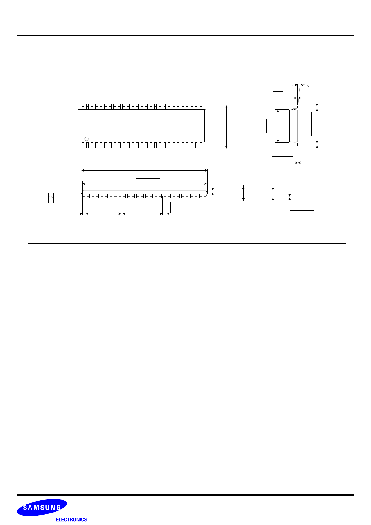
Package Physical Dimension
#54
#1
0.10
MAX
0.004
0.71
( )
0.028
0.30
0.012
22.62
0.891
22.22
0.875
+0.10
-0.05
+0.004
-0.002
MAX
± 0.10
± 0.004
0.80
0.0315
#28
#27
11. 76±0.20
0.21
0.008
0.463±0.008
± 0.05
± 0.002
Synchronous DRAM
0.05
0.002
0~8°C
0.45~0.75
0.50
MIN
0.018~0.030
)
0.020
(
1.00
0.039
± 0.10
± 0.004
0.25
0.010
10.16
0.125
0.005
1.20
0.047
TYP
0.400
+0.075
-0.035
+0.003
-0.001
MAX
54Pin TSOP(II) Package Dimension
4 of 14
Rev. 1.1 February 2006
K4S640832K
K4S641632K
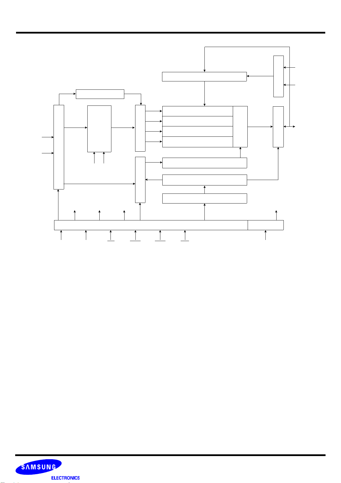
FUNCTIONAL BLOCK DIAGRAM
Bank Select
Refresh Counter
Row Buffer
Address Register
CLK
ADD
LRAS
LCBR
Synchronous DRAM
LWE
Data Input Register
LDQM
Row Decoder Col. Buffer
2M x 8 / 1M x 16
2M x 8 / 1M x 16
2M x 8 / 1M x 16
2M x 8 / 1M x 16
Column Decoder
Latency & Burst Length
Sense AMP
Output BufferI/O Control
DQi
LCKE
LRAS LCBR LWE LDQM
CLK CKE CS
Samsung Electronics reserves the right to change products or specification without notice.
*
LCAS LWCBR
Timing Register
RAS CAS WE L(U)DQM
Programming Register
5 of 14
Rev. 1.1 February 2006
 Loading...