

Samsung K4H280438B-TCB0, K4H280438B-TCA2, K4H280438B-TCA0, K4H281638B-TLA2, K4H281638B-TLA0 Datasheet
...
- 1 -
REV. 1.0 November. 2. 2000
128Mb DDR SDRAM
DDR SDRAM Specification
Version 1.0
- 2 -
REV. 1.0 November. 2. 2000
128Mb DDR SDRAM
Revision History
Version 0 (May, 1998)
- First version for internal review
Version 0.1(June, 1998)
- Added x4 organization
Version 0.2(Sep,1998)
1. Added "Issue prcharge command for all banks of the device" as the fourth step of power-up squence.
2. In power down mode timing diagram, NOP condition is added to precharge power down exit.
Version 0.3(Dec,1998)
- Added QFC Function.
- Added DC current value
- Reduce I/O capacitance values
Version 0.4(Feb,1999)
-Added DDR SDRAM history for reference(refer to the following page)
-Added low power version DC spec
Version 0.5(Apr,1999)
-Revised following first showing for JEDEC standard
-Added DC target current based on new DC test condition
Version 0.6(July 1,1999)
1.Modified binning policy
From To
-Z (133Mhz) -Z (133Mhz/266Mbps@CL=2)
-8 (125Mhz) -Y (133Mhz/266Mbps@CL=2.5)
-0 (100Mhz) -0 (100Mhz/200Mbps@CL=2)
2.Modified the following AC spec values
*1 : Changed description method for the same functionality. This means no difference from the previous version.
3.Changed the following AC parameter symbol
From. To.
Output data access time from CK/CK tDQCK tAC
Version 0.61(August 9,1999)
- Changed the some values of "write with auto precharge" table for different bank in page 31.
From. To.
-Z -0 -Z -Y -0
tAC +/- 0.75ns +/- 1ns +/- 0.75ns +/- 0.75ns +/- 0.8ns
tDQSCK +/- 0.75ns +/- 1ns +/- 0.75ns +/- 0.75ns +/- 0.8ns
tDQSQ +/- 0.5ns +/- 0.75ns +/- 0.5ns +/- 0.5ns +/- 0.6ns
tDS/tDH 0.5 ns 0.75 ns 0.5 ns 0.5 ns 0.6 ns
tCDLR
*1
2.5tCK-tDQSS 2.5tCK-tDQSS 1tCK 1tCK 1tCK
tPRE
*1
1tCK +/- 0.75ns 1tCK +/- 1ns 0.9/1.1 tCK 0.9/1.1 tCK 0.9/1.1 tCK
tRPST
*1
tCK/2 +/- 0.75ns tCK/2 +/- 1ns 0.4/0.6 tCK 0.4/0.6 tCK 0.4/0.6 tCK
tHZQ
*1
tCK/2 +/- 0.75ns tCK/2 +/- 1ns +/- 0.75ns +/- 0.75ns +/-0.8ns
Asserted
command
For Different Bank
3 4
Old New Old New
Read Legal Illegal Legal Illegal
Read + AP
*1
Legal Illegal Legal Illegal
- 3 -
REV. 1.0 November. 2. 2000
128Mb DDR SDRAM
Revision History(continued)
Version 0.7 (March, 2000)
- Changed 128Mb spec from target to Preliminary version.
- Changed partnames as follows.
- Changed input cap. spec.
- Changed operating condition.
- Added Overshoot/Undershoot spec
. Vih(max) = 4.2V, the overshoot voltage duration is ≤ 3ns at VDD.
. Vil(min) =- 1.5V, the overshoot voltage duration is ≤ 3ns at VSS.
- Changed AC parameters as follows.
- Added DC spec values.
Version 0.71 (April, 2000)
- Corrected a typo for tRAS at 133Mhz/CL2.5 from 48ns t0 45ns.
- Corrected a typo in "General Information" table from 64Mx4 to 8Mx16.
Version 0.72(May,2000)
- Changed DC spec item & test condition
Version 0.73(June,2000)
- Added updated DC spec values
- Deleted tDAL in AC parameter
Version 1.0(November,2000)
- Eliminate "preliminary"
from to
KM44L32031BT-G(L)Z/Y/0 K4H280438B-TC(L)A2/B0/A0
KM48L16031BT-G(L)Z/Y/0 K4H280838B-TC(L)A2/B0/A0
KM416L8031BT-G(L)Z/Y/0 K4H281638B-TC(L)A2/B0/A0
from to
CK/CK 2.5pF ~ 3.5pF 2.0pF ~ 3.0pF w/ Delta Cin = 0.25pF
DQ/DQS/DM 4.0pF ~ 5.5pF 4.0pF ~ 5.0pF w/ Delta Cin = 0.5pF
CMD/Addr 2.5pF ~ 3.5pF 2.0pF ~ 3.0pF with Delta Cin = 0.5pF
from to
Vil/Vih(ac) Vref +/- 0.35V Vref +/- 0.31V
VIL/VIH(dc) Vref +/- 0.18V Vref +/- 0.15V
from to Comments
tDQSQ +/- 0.5(PC266), +/- 0.6(PC200) +0.5(PC266), +0.6(PC200)
tDV +/- 0.35tCK - Removed
tQH -
tHPmin - 0.75ns(PC266)
New Definition
tHPmin - 1.0ns(PC200)
tHP - tCLmin or tCHmin New Definition

- 4 -
REV. 1.0 November. 2. 2000
128Mb DDR SDRAM
Contents
Revision History
General Information
1. Key Features
1.1 Features
1.2 Operating Frequencies
2. Package Pinout & Dimension
2.1 Package Pintout
2.2 Input/Output Function Description
2.3 66 Pin TSOP(II)/MS-024FC Package Physical Dimension
3. Functional Description
3.1 Simplified State Diagram
3.2 Basic Functionality
3.2.1 Power-Up Sequence
3.2.2 Mode Register Definition
3.2.2.1 Mode Register Set(MRS)
3.2.2.2 Extended Mode Register Set(EMRS)
3.2.3 Precharge
3.2.4 No Operation(NOP) & Device Deselect
3.2.5 Row Active
3.2.6 Read Bank
3.2.7 Write Bank
3.3 Essential Functionality for DDR SDRAM
3.3.1 Burst Read Operation
3.3.2 Burst Write Operation
3.3.3 Read Interrupted by a Read
3.3.4 Read Interrupted by a Write & Burst Stop
3.3.5 Read Interrupted by a Precharge
3.3.6 Write Interrupted by a Write
2
9
10
10
10
11
11
12
13
14
14
15
15
16
16
18
19
19
20
20
20
21
21
22
23
23
24
25

- 5 -
REV. 1.0 November. 2. 2000
128Mb DDR SDRAM
3.3.7 Write Interrupted by a Read & DM
3.3.8 Write Interrupted by a Precharge & DM
3.3.9 Burst Stop
3.3.10 DM masking
3.3.11 Read With Auto Precharge
3.3.12 Write With Auto Precharge
3.3.13 Auto Refresh & Self Refresh
3.3.14 Power Down
4. Command Truth Table
5. Functional Truth Table
6. Absolute Maximum Rating
7. DC Operating Conditions & Specifications
7.1 DC Operating Conditions
7.2 DC Specifications
8. AC Operating Conditions & Timming Specification
8.1 AC Operating Conditions
8.2 AC Timming Parameters & Specification
9. AC Operating Test Conditions
10. Input/Output Capacitance
11. IBIS: I/V Characteristics for Input and Output Buffers
11.1 Normal strength driver
11.2 Half strength driver( will be included in the future)
12. QFC function
QFC definition
QFC timming on Read Operation
QFC timming on Write operation with tDQSSmax
QFC timming on Write operation with tDQSSmin
QFC timming example for interrupted writes operation
Timing Diagram
26
27
28
29
30
31
32
33
34
35
40
40
41
42
42
43
45
45
46
46
48
49
49
49
50
50
51
52

- 6 -
REV. 1.0 November. 2. 2000
128Mb DDR SDRAM
Table 1 : Operating frequency and DLL jitter
Table 2. : Column address configurtion
Table 3 : Input/Output function description
Table 4 : Burst address ordering for burst length
Table 5 : Bank selection for precharge by bank address bits
Table 6 : Operating description when new command asserted while
read with auto precharge is issued
Table 7 : Operating description when new command asserted while
write with auto precharge is issued
Table 8 : Command truth table
Table 9-1 : Functional truth table
Table 9-2 : Functional truth table (contiued)
Table 9-3 : Functional truth table (contiued)
Table 9-4 : Functional truth table (contiued)
Table 9-5 : Functional truth table (cotinued)
Table 10 : Absolute maximum raings
Table 11 : DC operating condtion
Table 12 : DC specification
Table 13 : AC operating condition
Table 14 : AC timing parameters and specifications
Table 15 : AC operating test conditions
Table 16 : Input/Output capacitance
Table 17 : Pull down and pull up current values
List of tables
10
11
12
17
19
30
31
34
35
36
37
38
39
40
40
42
42
44
45
45
47

- 7 -
REV. 1.0 November. 2. 2000
128Mb DDR SDRAM
Figure 1 : 128Mb Package Pinout
Figure 2 : Package dimension
Figure 3 :State digram
Figure 4 : Power up and initialization sequence
Figure 5 : Mode register set
Figure 6 : Mode register set sequence
Figure 7 : Extend mode register set
Figure 8 : Bank activation command cycle timing
Figure 9 : Burst read operation timing
Figure 10 : Burst write operation timing
Figure 11 : Read interrupted by a read timing
Figure 12 : Read interrupted by a write and burst stop timing
Figure 13 : Read interrupted by a precharge timing
Figure 14 : Write interrupted by a write timing
Figure 15 : Write interrupted by a read and DM timing
Figure 16 : Write interrupted by a precharge and DM timing
Figure 17 : Burst stop timing
Figure 18 : DM masking timing
Figure 19 : Read with auto precharge timing
Figure 20 : Write with auto precharge timing
Figure 21 : Auto refresh timing
Figure 22 : Self refresh timing
Figure 23 : Power down entry and exit timing
Figure 24 : Output Load Circuit (SSTL_2)
Figure 25 : I / V characteristics for input/output buffers:
pull-up(above) and pull-down(below)
Figure 26 : QFC timing on read operation
Figure 27 : QFC timing on write operation with tDQSSmax
Figure 28 : QFC timing on write operation with tDQSSmin
Figure 29 : QFC timing example for interrupted writes operation
List of figures
11
13
14
15
16
17
18
20
21
22
23
23
24
25
26
27
28
29
30
31
32
32
33
45
46
49
50
50
51
- 8 -
REV. 1.0 November. 2. 2000
128Mb DDR SDRAM
General Information
Organization 133Mhz w/ CL=2 133Mhz w/ CL=2.5 100Mhz w/ CL=2
32Mx4
K4H280438B-TCA2 K4H280438B-TCB0 K4H280438B-TCA0
K4H280438B-TLA2 K4H280438B-TLB0 K4H280438B-TLA0
16Mx8
K4H280838B-TCA2 K4H280838B-TCB0 K4H280838B-TCA0
K4H280838B-TLA2 K4H280838B-TLB0 K4H280838B-TLA0
8Mx16
K4H281638B-TCA2 K4H281638B-TCB0 K4H281638B-TCA0
K4H281638B-TLA2 K4H281638B-TLB0 K4H281638B-TLA0
T : TSOP2 (400mil x 875mil)
A0 : 10ns@CL2
A2 : 7.5ns@CL2
B0 : 7.5ns@CL2.5
C : (Commercial, Normal)
L : (Commercial, Low)
04 : x4
08 : x8
16 : x16
32 : x32
64 : 64M 4K/64ms
28 : 128M 4K/64ms
56 : 256M 8K/64ms
51 : 512M 8K/64ms
1G : 1G 16K/32ms
H : DDR SDRAM
M : 1st Generation
A : 2nd Generation
B : 3rd Generation
C : 4th Generation
D : 5th Generation
E : 6th Generation
K 4 H XX XX X X X - X X
Memory
DRAM
Small Classification
Density and Refresh
Temperature & Power
Package
Organization
Version
Interface (VDD & VDDQ)
1. SAMSUNG Memory : K
2. DRAM : 4
3. Small Classification
4. Density & Refresh
5. Organization
8. Version
9. Package
10. Temperature & Power
11. Speed
3 : 4 Bank
6. Bank
1 2 3 4 5 6 7 8 9 10 11
XX
8: SSTL-2(2.5V, 2.5V)
7. Interface (VDD & VDDQ)
Speed
Bank
- 9 -
REV. 1.0 November. 2. 2000
128Mb DDR SDRAM
• Double-data-rate architecture; two data transfers per clock cycle
• Bidirectional data strobe(DQS)
• Four banks operation
• Differential clock inputs(CK and CK)
• DLL aligns DQ and DQS transition with CK transition
• MRS cycle with address key programs
-. Read latency 2, 2.5 (clock)
-. Burst length (2, 4, 8)
-. Burst type (sequential & interleave)
• All inputs except data & DM are sampled at the positive going edge of the system clock(CK)
• Data I/O transactions on both edges of data strobe
• Edge aligned data output, center aligned data input
• LDM,UDM/DM for write masking only
• Auto & Self refresh
• 15.6us refresh interval(4K/64ms refresh)
• Maximum burst refresh cycle : 8
• 66pin TSOP II package
1. Key Features
1.1 Features
1.2 Operating Frequencies
*CL : Cas Latency
Table 1. Operating frequency and DLL jitter
- A2(DDR266A) - B0(DDR266B) - A0(DDR200)
Speed @CL2 133MHz@CL2 100MHz 100MHz
Speed @CL2.5 - 133MHz -
DLL jitter ±0.75ns ±0.75ns ±0.8ns
- 10 -
REV. 1.0 November. 2. 2000
128Mb DDR SDRAM
VDD
1
66 PIN TSOP(II)
(400mil x 875mil)
DQ0
2
VDDQ
3
NC
4
DQ1
5
VSSQ
6
NC
7
DQ2
8
VDDQ
9
NC
10
DQ3 11
VSSQ 12
BA0
20
CS
19
RAS
18
CAS
17
WE
16
NC
15
VDDQ
14
NC 13
VDD
27
A3
26
A2
25
A1
24
A0
23
AP/A10
22
BA1
21
VSS
54
DQ7
53
VSSQ
52
NC
51
DQ6
50
VDDQ
49
NC
48
DQ5
47
VSSQ
46
NC
45
DQ4
44
VDDQ
43
A11
35
36
CKE
37
CK
38
DM
39
VREF
40
VSSQ
41
NC
42
VSS
55
A4
56
A5
57
A6
58
A7
59
A8
60
A9
34
(0.65 mm PIN PITCH)
33
32
31
30
29
28
61
62
63
64
65
66
NC
NC
NC
QFC/NC
NC
VDD
NC
DQS
NC
VSS
CK
NC
NC
32Mb x 4
16Mb x 8
VSS
NC
VSSQ
NC
DQ3
VDDQ
NC
NC
VSSQ
NC
DQ2
VDDQ
A11
CKE
CK
DM
VREF
VSSQ
NC
VSS
A4
A5
A6
A7
A8
A9
NC
DQS
NC
VSS
CK
NC
NC
VDD
NC
VDDQ
NC
DQ0
VSSQ
NC
NC
VDDQ
NC
DQ1
VSSQ
BA0
CS
RAS
CAS
WE
NC
VDDQ
NC
VDD
A3
A2
A1
A0
AP/A10
BA1
NC
NC
NC
QFC/NC
NC
VDD
Bank Address
BA0-BA1
Row Address
A0-A11
Auto Precharge
A10
MS-024FC
Organization Column Address
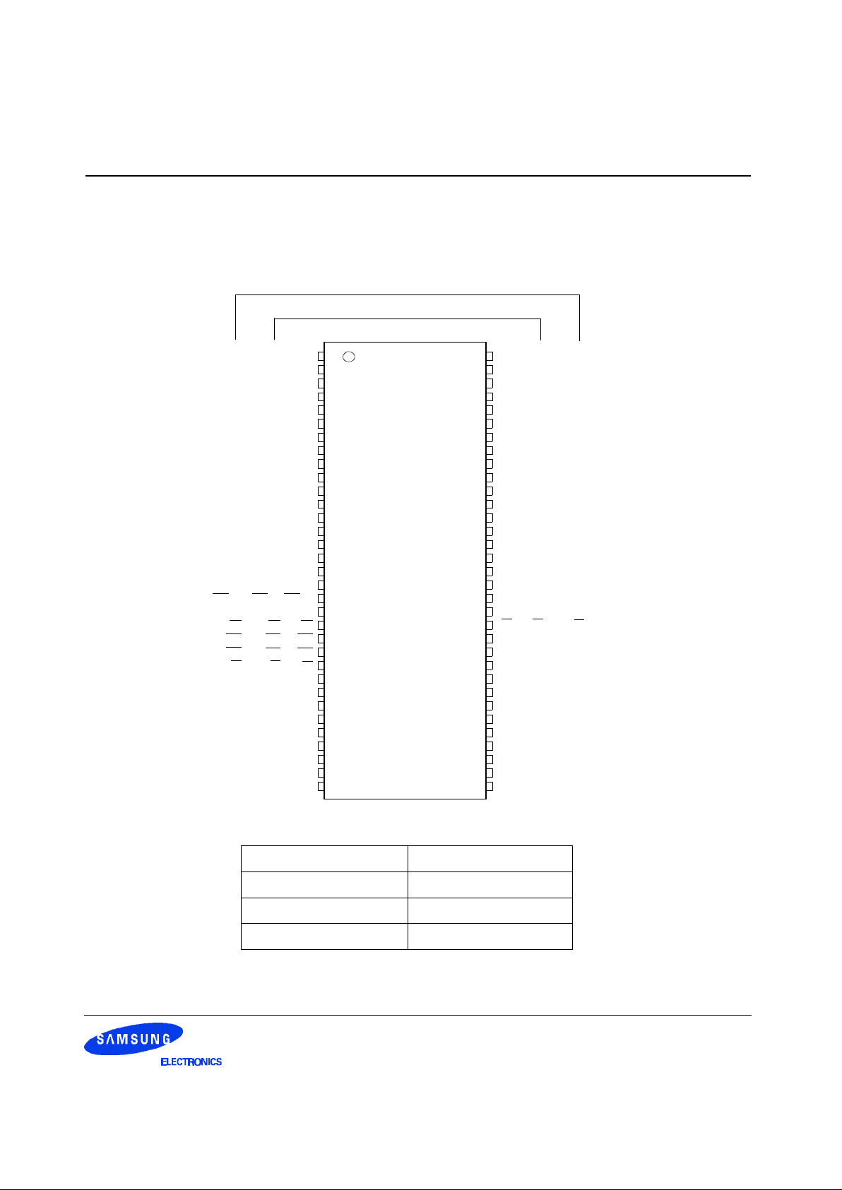
32Mx4 A0-A9, A11
16Mx8 A0-A9
8Mx16 A0-A8
DM is internally loaded to match DQ and DQS identically.
2.1 Package Pinout
FIgure 1. 128Mb package Pinout
Table 2. Column address configuration
1. Package Pinout & Dimension
VDD
DQ0
VDDQ
DQ1
DQ2
VSSQ
DQ3
DQ4
VDDQ
DQ5
DQ6
VSSQ
BA0
CS
RAS
CAS
WE
LDM
VDDQ
DQ7
VDD
A3
A2
A1
A0
AP/A10
BA1
NC
LDQS
NC
QFC/NC
NC
VDD
VSS
DQ15
VSSQ
DQ14
DQ13
VDDQ
DQ12
DQ11
VSSQ
DQ10
DQ9
VDDQ
A11
CKE
CK
UDM
VREF
VSSQ
DQ8
VSS
A4
A5
A6
A7
A8
A9
NC
UDQS
NC
VSS
CK
NC
NC
8Mb x 16
- 11 -
REV. 1.0 November. 2. 2000
128Mb DDR SDRAM
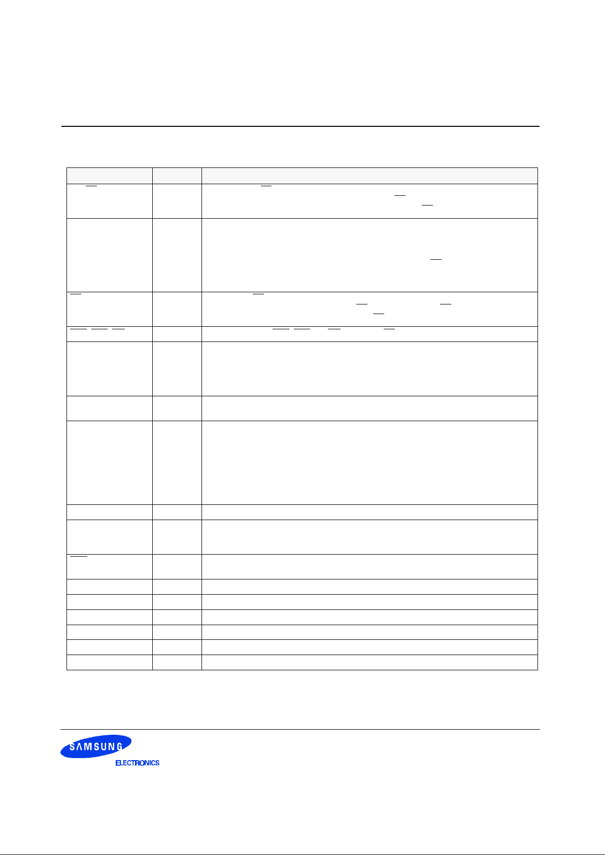
2.2 Input/Output Function Description
Table 3. Input/Output Function Description
SYMBOL TYPE DESCRIPTION
CK, CK Input Clock : CK and CK are differential clock inputs. All address and control input signals are sam-
pled on the positive edge of CK and negative edge of CK. Output (read) data is referenced to
both edges of CK. Internal clock signals are derived from CK/CK.
CKE Input Clock Enable : CKE HIGH activates, and CKE LOW deactivates internal clock signals, and
device input buffers and output drivers. Deactivating the clock provides PRECHARGE
POWER-DOWN and SELF REFRESH operation (all banks idle), or ACTIVE POWER-DOWN
(row ACTIVE in any bank). CKE is synchronous for all functions except for disabling outputs,
which is achieved asynchronously. Input buffers, excluding CK, CK and CKE are disabled
during power-down and self refresh modes, providing low standby power. CKE will recognize
an LVCMOS LOW level prior to VREF being stable on power-up.
CS Input Chip Select : CS enables(registered LOW) and disables(registered HIGH) the command
decoder. All commands are masked when CS is registered HIGH. CS provides for external
bank selection on systems with multiple banks. CS is considered part of the command code.
RAS, CAS, WE Input Command Inputs : RAS, CAS and WE (along with CS) define the command being entered.
LDM,(U)DM Input Input Data Mask : DM is an input mask signal for write data. Input data is masked when DM is
sampled HIGH along with that input data during a WRITE access. DM is sampled on both
edges of DQS. DM pins include dummy loading internally, to matches the DQ and DQS load-
ing. For the x16, LDM corresponds to the data on DQ0-DQ7 ; UDM correspons to the data on
DQ8-DQ15.
BA0, BA1 Input Bank Addres Inputs : BA0 and BA1 define to which bank an ACTIVE, READ, WRITE or PRE-
CHARGE command is being applied.
A [n : 0] Input Address Inputs : Provide the row address for ACTIVE commands, and the column address
and AUTO PRECHARGE bit for READ/WRITE commands, to select one location out of the
memory array in the respective bank. A10 is sampled during a PRECHARGE command to
determine whether the PRECHARGE applies to one bank (A10 LOW) or all banks (A10
HIGH). If only one bank is to be precharged, the bank is selected by BA0, BA1. The address
inputs also provide the op-code during a MODE REGISTER SET command. BA0 and BA1
define which mode register is loaded during the MODE REGISTER SET command (MRS or
EMRS).
DQ I/O Data Input/Output : Data bus
LDQS,(U)DQS I/O Data Strobe : Output with read data, input with write data. Edge-aligned with read data, cen-
tered in write data. Used to capture write data. For the x16, LDQS corresponds to the data on
DQ0-DQ7 ; UDQS corresponds to the data on DQ8-DQ15.
QFC Output FET Control : Optional. Output during every Read and Write access. Can be used to control
isolation switches on modules.
NC - No Connect : No internal electrical connection is present.
VDDQ Supply DQ Power Supply : +2.5V ± 0.2V.
VSSQ Supply DQ Ground.
VDD Supply Power Supply : +2.5V ± 0.2V (device specific).
VSS Supply Ground.
VREF Input SSTL_2 reference voltage.
- 12 -
REV. 1.0 November. 2. 2000
128Mb DDR SDRAM
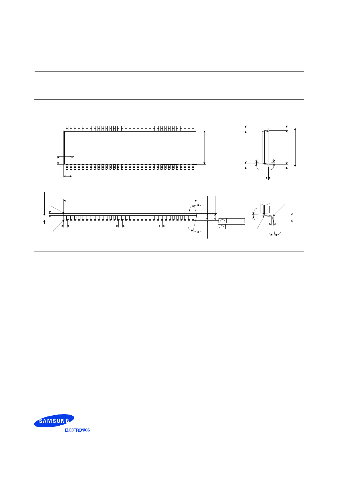
2.3 66 Pin TSOP(II)/MS-024FC Package Physical Dimension
Units : Millimeters
0.30±0.08
0.65TYP(0.71)
22.22±0.10
0.125
(0.80)
10.16±0.10
0×~8×
#1 #33
#66 #34
(1.50)
(1.50)
0.65±0.08
1.00±0.10
1.20MAX
(0.50) (0.50)(10.76)
11.76±0.20
(10×)(10×)
+0.075
-0.035
(0.80)
0.10 MAX
0.075 MAX
[ ]
0.05 MIN
(10×)
(10×)
(
R
0
.
1
5
)
0.210±0.05
0.665±0.05
(R
0.
1
5)
(
4
×
)
(
R
0
.
2
5
)
(
R0
.2
5)
0.45~0.75
0.25TYP
NOTE
1. ( ) IS REFERENCE
2. [ ] IS ASS’Y OUT QUALITY
Figure 2. Package dimension
- 13 -
REV. 1.0 November. 2. 2000
128Mb DDR SDRAM
3. Functional Description
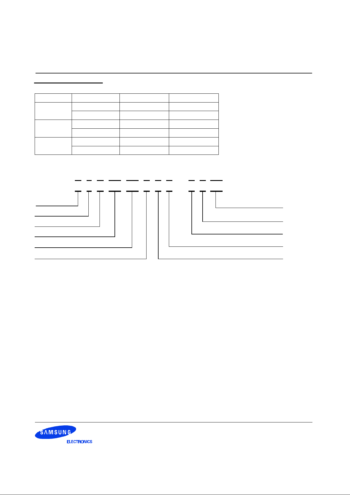
3.1 Simplified State Diagram
READ
SELF
REFRESH
AUTO
REFRESH
POWER
DOWN
ROW
ACTIVE
READAWRITEA
WRITEA
PRE
CHARGE
POWER
ON
IDLE
MODE
POWER
DOWN
REGISTER
SET
REFS
REFSX
REFA
MRS
CKEL
CKEH
ACT
CKEL
CKEH
WRITE
WRITE
WRITEA
PRE
PRE
POWER
APPLIED
READA
PRE
PRE
READA
WRITEA READA
READ
READ
Automatic Sequence
Command Sequence
BURST STOP
WRITEA : Write with autoprecharge
READA : Read with autoprecharge
Figure 3. State diagram
- 14 -
REV. 1.0 November. 2. 2000
128Mb DDR SDRAM
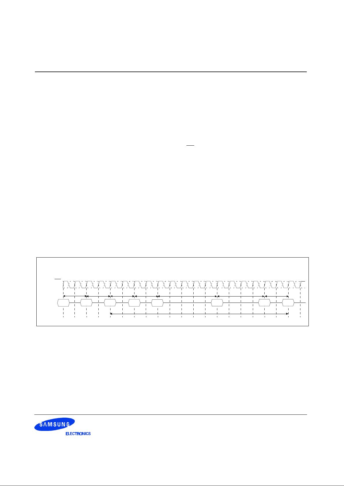
3.2.1 Power-Up and Initialization Sequence
The following sequence is required for POWER UP and Initialization.
1. Apply power and attempt to maintain CKE at a low state(all other inputs may be undefined.)
- Apply VDD before or at the same time as VDDQ.
- Apply VDDQ before or at the same time as VTT & Vref.
2. Start clock and maintain stable condition for a minimum of 200us.
3. The minimum of 200us after stable power and clock(CK, CK), apply NOP & take CKE high.
4. Issue precharge commands for all banks of the device.
5. Issue EMRS to enable DLL.(To issue "DLL Enable" command, provide "Low" to A0, "High" to BA0 and "Low"
to all of the rest address pins, A1~A11 and BA1)
6. Issue a mode register set command for "DLL reset". The additional 200 cycles of clock input is required to
lock the DLL.
(To issue DLL reset command, provide "High" to A8 and "Low" to BA0)
7. Issue precharge commands for all banks of the device.
8. Issue 2 or more auto-refresh commands.
9. Issue a mode register set command with low to A8 to initialize device operation.
*1 Every "DLL enable" command resets DLL. Therefore sequence 6 can be skipped during power up.
Instead of it, the additional 200 cycles of clock input is required to lock the DLL after enabling DLL.
*2 Sequence of 6 & 7 is regardless of the order.
Power up & Initialization Sequence
Command
0 1 2 3 4 5 6 7 8 9 10 11 12 13 14 15 16 17 18 19
tRP
2 Clock min.
precharge
ALL Banks
2nd Auto
Refresh
Mode
Register Set
Any
Command
tRFC
1st Auto
Refresh
tRFC
min.200 Cycle
EMRS
MRS
2 Clock min.
DLL Reset
*1
*2
*1
2 Clock min.
∼
∼
∼
∼
∼
∼
∼
∼
∼
∼
∼
∼
∼
∼
∼
∼
precharge
ALL Banks
tRP
CK
CK
3.2 Basic Functionality
Figure 4. Power up and initialization sequence
- 15 -
REV. 1.0 November. 2. 2000
128Mb DDR SDRAM
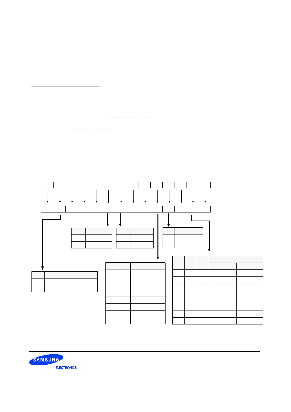
3.2.2 Mode Register Definition
3.2.2.1 Mode Register Set(MRS)
The mode register stores the data for controlling the various operating modes of DDR SDRAM. It programs
CAS latency, addressing mode, burst length, test mode, DLL reset and various vendor specific options to make
DDR SDRAM useful for variety of different applications. The default value of the mode register is not defined,
therefore the mode register must be written after EMRS setting for proper DDR SDRAM operation. The mode
register is written by asserting low on CS, RAS, CAS, WE and BA0(The DDR SDRAM should be in all bank precharge with CKE already high prior to writing into the mode register). The states of address pins A0 ~ A11 in
the same cycle as CS, RAS, CAS, WE and BA0 going low are written in the mode register. Two clock cycles
are requested to complete the write operation in the mode register. The mode register contents can be
changed using the same command and clock cycle requirements during operation as long as all banks are in
the idle state. The mode register is divided into various fields depending on functionality. The burst length uses
A0 ~ A2, addressing mode uses A3, CAS latency(read latency from column address) uses A4 ~ A6. A7 is used
for test mode. A8 is used for DLL reset. A7 must be set to low for normal MRS operation. Refer to the table for
specific codes for various burst lengths, addressing modes and CAS latencies.
Address Bus
CAS Latency
A6 A5 A4 Latency
0 0 0 Reserved
0 0 1 Reserved
0 1 0 2
0 1 1 Reserved
1 0 0 Reserved
1 0 1 Reserved
1 1 0 2.5
1 1 1 Reserved
Burst Length
A2 A1 A0
Latency
Sequential Interleave
0 0 0 Reserve Reserve
0 0 1 2 2
0 1 0 4 4
0 1 1 8 8
1 0 0 Reserve Reserve
1 0 1 Reserve Reserve
1 1 0 Reserve Reserve
1 1 1 Reserve Reserve
A7 mode
0 Normal
1 Test
A3 Burst Type
0 Sequential
1 Interleave
* RFU(Reserved for future use)
should stay "0" during MRS
cycle.
A8 DLL Reset
0 No
1 Yes
Mode Register
BA1 BA0 A11 A10 A9 A8 A7 A6 A5 A4 A3 A2 A1 A0
RFU TM CAS Latency BT Burst LengthRFU DLL 0
BA0 An ~ A0
0 (Existing)MRS Cycle
1 Extended Funtions(EMRS)
Figure 5. Mode Register Set
- 16 -
REV. 1.0 November. 2. 2000
128Mb DDR SDRAM
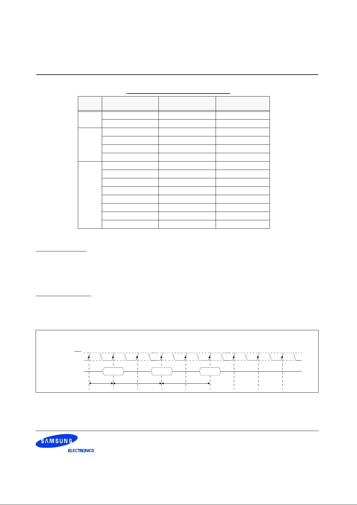
Mode Register Set
*1 : MRS can be issued only at all bank precharge state.
*2 : Minimum tRP is required to issue MRS command.
Command
20 1 53 4 86 7
tCK
2 Clock min.
Precharge
All Banks
Mode
Register Set
tRP
*2
*1
Any
Command
CK
CK
Burst Address Ordering for Burst Length
Burst
Length
Starting
Address(A2, A1, A0)
Sequential Mode Interleave Mode
2
xx0 0, 1 0, 1
xx1 1, 0 1, 0
4
x00 0, 1, 2, 3 0, 1, 2, 3
x01 1, 2, 3, 0 1, 0, 3, 2
x10 2, 3, 0, 1 2, 3, 0, 1
x11 3, 0, 1, 2 3, 2, 1, 0
8
000 0, 1, 2, 3, 4, 5, 6, 7 0, 1, 2, 3, 4, 5, 6, 7
001 1, 2, 3, 4, 5, 6, 7, 0 1, 0, 3, 2, 5, 4, 7, 6
010 2, 3, 4, 5, 6, 7, 0, 1 2, 3, 0, 1, 6, 7, 4, 5
011 3, 4, 5, 6, 7, 0, 1, 2 3, 2, 1, 0, 7, 6, 5, 4
100 4, 5, 6, 7, 0, 1, 2, 3 4, 5, 6, 7, 0, 1, 2, 3
101 5, 6, 7, 0, 1, 2, 3, 4 5, 4, 7, 6, 1, 0, 3, 2
110 6, 7, 0, 1, 2, 3, 4, 5 6, 7, 4, 5, 2, 3, 0, 1
111 7, 0, 1, 2, 3, 4, 5, 6 7, 6, 5, 4, 3, 2, 1, 0
DLL Enable/Disable
The DLL must be enabled for normal operation. DLL enable is required during power-up initialization, and
upon returing to normal operation after having disabled the DLL for the purpose of debug or evaluation (upon
exiting Self Refresh Mode, the DLL is enabled automatically). Any time the DLL is enabled, 200 clock cycles
must occur before a READ command can be issued.
Output Drive Strength
The normal drive strength for all outputs is specified to be SSTL_2, Class II. Some vendors might also support
a weak driver strength option, intended for lighter load and/or point-to-point environments. I-V curves for the
normal drive strength and weak drive strength will be included in a future revision of this document.
Table 4. Burst address ordering for burst length
Figure 6. Mode Register Set sequence
 Loading...