


Samsung K4D263238F-QC50, K4D263238F-QC40 Datasheet

K4D263238F
128M DDR SDRAM
128Mbit DDR SDRAM
1M x 32Bit x 4 Banks
Double Data Rate Synchronous DRAM
with Bi-directional Data Strobe and DLL
Revision 1.1
May 2003
- 1 -
Rev 1.1 (May 2003)
K4D263238F
Revision History
Revision 1.1 (May 30, 2003)
• Added Lead Free package part number in the datasheet.
Revision 1.0 (April 29, 2003)
• Define DC spec.
Revision 0.0 (January 20, 2003)- Target spec
• Define target spec.
128M DDR SDRAM
- 2 -
Rev 1.1 (May 2003)
K4D263238F
1M x 32Bit x 4 Banks Double Data Rate Synchronous DRAM
with Bi-directional Data Strobe and DLL
FEATURES
128M DDR SDRAM
• 2.5V ± 5% power supply for device operation
• 2.5V ± 5% power supply for I/O interface
• SSTL_2 compatible inputs/outputs
• 4 banks operation
• MRS cycle with address key programs
-. Read latency 3 (clock)
-. Burst length (2, 4, 8 and Full page)
-. Burst type (sequential & interleave)
• Full page burst length for sequential burst type only
• Start address of the full page burst should be even
• All inputs except data & DM are sampled at the positive
going edge of the system clock
• Differential clock input
• No Write Interrupted by Read function
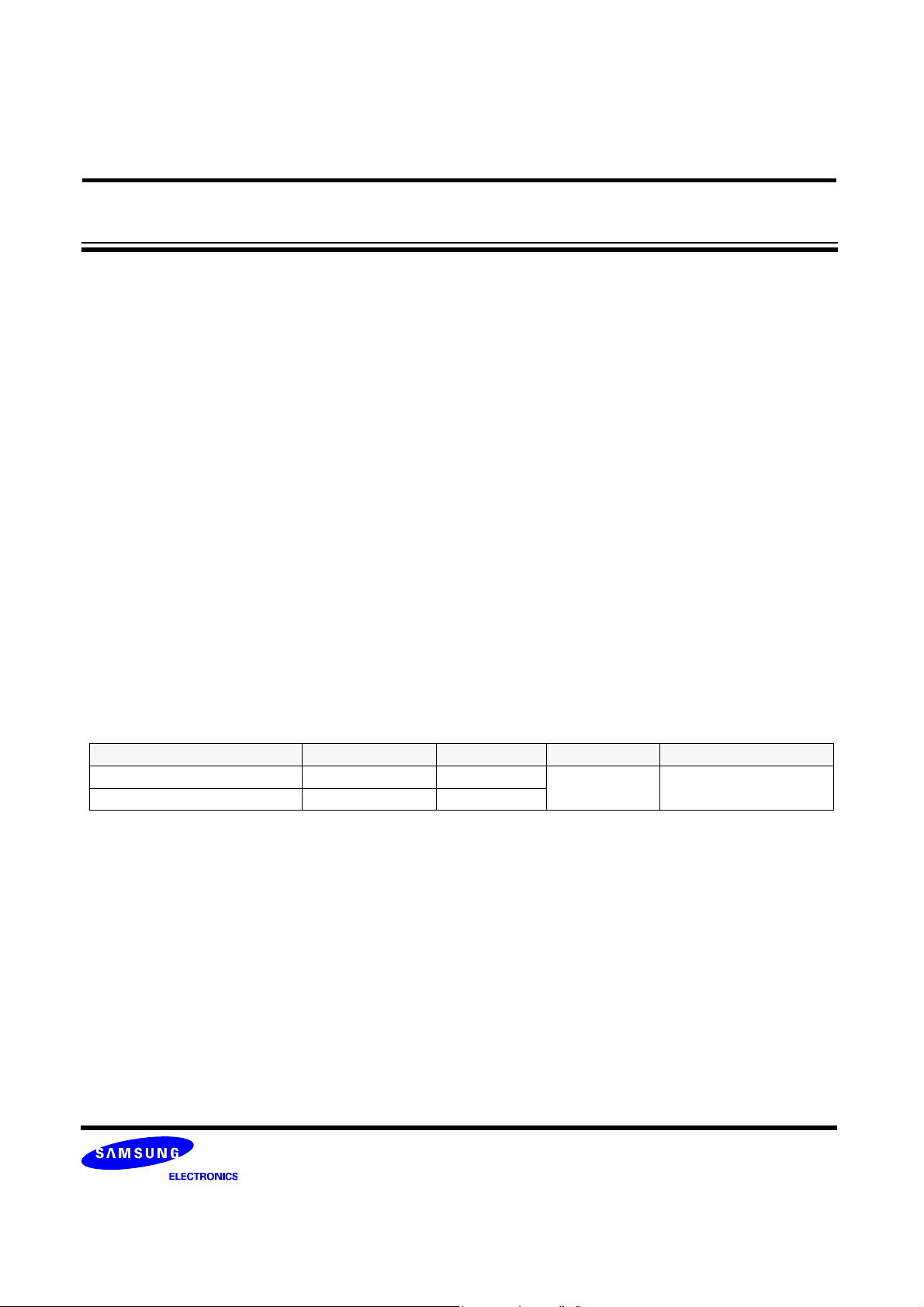
ORDERING INFORMATION
Part NO. Max Freq. Max Data Rate Interface Package
K4D263238F-QC40 250MHz 500Mbps/pin
K4D263238F-QC50 200MHz 400Mbps/pin
K4D263238F-UC is the Lead Free package part number.
• Data I/O transactions on both edges of Data strobe
• DLL aligns DQ and DQS transitions with Clock transition
• Edge aligned data & data strobe output
• Center aligned data & data strobe input
• DM for write masking only
• Auto & Self refresh
• 32ms refresh period (4K cycle)
• 100pin TQFP package
• Maximum clock frequency up to 250MHz
• Maximum data rate up to 500Mbps/pin
SSTL_2 100 TQFP
GENERAL DESCRIPTION
FOR 1M x 32Bit x 4 Bank DDR SDRAM
The K4D263238F is 134,217,728 bits of hyper synchronous data rate Dynamic RAM organized as 4 x 1,048,576 words by
32 bits, fabricated with SAMSUNG′s high performance CMOS technology. Synchronous features with Data Strobe allow
extremely high performance up to 2.0GB/s/chip. I/O transactions are possible on both edges of the clock cycle. Range of
operating frequencies, programmable burst length and pro grammable latencies allow the d evice to be useful for a variety
of high performance memory system applications.
- 3 -
Rev 1.1 (May 2003)
K4D263238F
PIN CONFIGURATION (Top View)
DQ28
VDDQ
DQ27
DQ26
VSSQ
DQ25
DQ24
VDDQ
DQ15
DQ14
VSSQ
128M DDR SDRAM
DQ13
DQ12
VDDQ
VSS
VDD
DQ11
DQ10
VSSQ
DQ9
DQ8
VDDQ
VREF
DM3
DM1CKCK
CKE
MCL
A8(AP)
DQ29
VSSQ
DQ30
DQ31
VSS
VDDQ
N.C
N.C
N.C
N.C
N.C
VSSQ
RFU
DQS
VDDQ
VDD
DQ0
DQ1
VSSQ
DQ2
8079787776757473727170696867666564636261605958575655545352
81
82
83
84
85
86
87
88
89
90
91
92
93
94
95
96
97
98
99
100
1234567891011121314151617181920212223242526272829
DQ3
DQ4
DQ5
DQ6
DQ7
VDDQ
VSSQ
VDDQ
DQ16
100 Pin TQFP
20 x 14 mm
0.65mm pin Pitch
DQ17
DQ18
DQ19
VSSQ
VDDQ
VDD
VSS
2
DM0
DQ20
DQ21
DQ22
DQ23
VSSQ
VDDQ
DM2
WE
CAS
RAS
CS
51
50
A7
49
A6
48
A5
47
A4
46
VSS
45
A9
44
N.C
43
N.C
42
N.C
41
N.C
40
N.C
39
N.C
38
N.C
37
A11
36
A10
35
VDD
34
A3
33
A2
32
A1
31
A0
30
BA0
BA1
PIN DESCRIPTION
CK,CK Differential Clock Input BA0, BA1 Bank Select Address
CKE Clock Enable A0 ~A11 Address Input
CS Chip Select DQ0 ~ DQ31 Data Input/Output
RAS
CAS
WE Write Enable VDDQ Power for DQ′s
DQS Data Strobe VSSQ Ground for DQ′s
DMi Data Mask MCL Must Connect Low
RFU Reserved for Future Use
Row Address Strobe VDD Power
Column Address Strobe VSS Ground
- 4 -
Rev 1.1 (May 2003)
K4D263238F
128M DDR SDRAM
INPUT/OUTPUT FUNCTIONAL DESCRIPTION
Symbol Type Function
The differential system clock Input.
CK, CK
*1
CKE Input
CS Input
RAS
CAS Input
WE Input
DQS Input/Output Data input and output are synchronized with both edge of DQS.
DM0 ~ DM3 Input
DQ0 ~ DQ31 Input/Output Data inputs/Outputs are multiplexed on the same pins.
BA0, BA1 Input Selects which bank is to be active.
A0 ~ A11 Input
DD/VSS Power Supply Power and ground for the input buffers and core logic.
V
VDDQ/VSSQ Power Supply
VREF Power Supply Reference voltage for inputs, used for SSTL interface.
MCL Mus t Connect Low Must connect Low
*1 : The timing reference point for the differential clocking is the cross point of CK and CK.
For any applications using the single ended clocking, apply V
Input
Input
All of the inputs are sampled on the rising edge of the clock except
DQ′s and DM′s that are sampled on both edges of the DQS.
Activates the CK signal when high and deactivates the CK signal
when low. By deactivating the clock, CKE low indicates the Power
down mode or Self refresh mode.
CS enables the command decoder when low an d di sa bl e d th e command decoder when high. When the command decoder is disabled,
new commands are ignored but previous operations continue.
Latches row addresses on the positive going edge of the CK with
RAS
low. Enables row access & precharge.
Latches column addresses on the positive going edge of the CK with
CAS low. Enables column access.
Enables write operation and row precharge.
Latches data in starting from CAS, WE active.
Data In mask. Data In is masked by DM Latency=0 when DM is high
in burst write. DM0 for DQ0 ~ DQ7, DM1 for DQ8 ~ DQ15, DM2 for
DQ16 ~ DQ23, DM3 for DQ24 ~ DQ31.
Row/Column addresses are multiplexed on the same pins.
Row addresses : RA0 ~ RA11, Column addresses : CA0 ~ CA7.
Column address CA8 is used for auto precharge.
Isolated power supply and ground for the output buffers to provide
improved noise immunity.
REF to CK pin.
- 5 -
Rev 1.1 (May 2003)

K4D263238F
BLOCK DIAGRAM (1Mbit x 32I/O x 4 Bank)
128M DDR SDRAM
32
Intput Buffer
LWE
CK,CK
ADDR
LCKE
Address Register
Bank Select
LRAS
Refresh Counter
Row Buffer
LCBR
LRAS
LCBR
LWE
CK, CK
Row Decoder
Col. Buffer
LCAS
Data Input Register
Serial to parallel
64
1Mx32
1Mx32
1Mx32
1Mx32
Column Decoder
Latency & Burst Length
Programming Register
LWCBR
Sense AMP
2-bit prefetch
64 32
DLL
CK,CK
LDMi
Output BufferI/O Control
x32
DQi
Strobe
Gen.
LDMi
Data Strobe
CK,CK
Timing Register
CKE CS RAS CAS WE DMi
- 6 -
Rev 1.1 (May 2003)