


查询K4C89083AF-ACF5供应商
K4C89183AF
288Mb x18 Network-DRAM2 Specification
Version 0.7
- 1 -
REV. 0.7 Jan. 2005
K4C89183AF
Revision History
Version 0.0 (Oct. 2002)
- First Release
Version 0.01 (Nov. 2002)
- Changed die revision from D-die to F-die
- Corrected typo
- Corrected DQS to DS and QS(DQS -> DS and QS) in AC timing table and timing diagram.
Version 0.1 (Apr. 2003)
- Added 800Mbps(400Mhz) product
- Changed operating temperature from Ta to Tc.
- Changed capacitance of ADDR/CMD/CLK
From To
Min Max Min Max
Addr/CMD/CLK 1.5 2.5 1.5 3.0
- Changed tDSS(DS input Falling Edge to Clock Setup Time)
From To
F6 FB F5 G7 F6 FB F5
CL4 0.9 0.9 1.0 0.75 0.75 0.8 1.0
CL5 0.9 0.9 1.0 0.75 0.75 0.8 1.0
CL6 0.9 0.9 1.0 0.75 0.75 0.8 1.0
CL7 - - - 0.75 - - -
- Added CL7 for 800Mbps
- Deleted TSOP package outline
Version 0.11 (Apr. 2003)
- Corrected typo in page 3.(Deleted bi-directional strobe)
- Corrected min. Vref to VDDQ/2x95% in page 7
Version 0.2 (Aug. 2003)
- Added package physical dimension
- Extracted 800Mbps(G7) binning from target spec ( G7 will be added in the future)
- Changed DC test condition
From To Changed point
IDD1S,IDD2N,IDD2P,IDD5,IDD6 IDD1S,IDD2N,IDD2P,IDD5B,IDD6 Changed condition
- IDD4W, IDD4R newly inserted
- Changed low frequency spec like below
From To
Unit : ns F6 FB F5 F6 FB F5
tCK max@CL=4 7.5 7.5 7.5 6.0 6.0 6.0
tCK max@CL=5 7.5 7.5 7.5 6.0 6.0 6.0
tCK max@CL=6 7.5 7.5 7.5 6.0 6.0 6.0
- Changed AC test load picture
Version 0.3 (Nov. 2003)
- Changed Packge type from die-exposed to full molded
- Changed Package code in Partnumber
- 2 -
REV. 0.7 Jan. 2005
K4C89183AF
Version 0.31 (Mar., 2004)
- Corrected typo. in page 7 (Changed operating Temperature to 85’C, case temperature)
Version 0.4 (Jun., 2004)
- Changed from "target" to "Preliminary"
- Changed min. tCK@CL5 to 3.5ns in "-F6"
From To
F6 F6
CL = 4 4.0 ns 4.0 ns
t
Clock Cycle Time (min)
CK
Version 0.5 (Aug., 2004)
- Deleted self-refresh function and BL2 from spec
Version 0.51 (Aug., 2004)
- Corrected error in page 54, "Package Out line Drawing". (Just 4 balls were missing in drawing)
Version 0.6 (Nov., 2004)
- Deleted "preliminary"
- Changed current value in page 9
Version 0.7 (Jan., 2005)
- Deleted the tDQSQA in page 11
- Deleted the tSSK in page 11
CL = 5 3.33 ns 3.5 ns
CL = 6 3.0ns 3.0ns
- 3 -
REV. 0.7 Jan. 2005
K4C89183AF
4,194,304-WORDS x 4 BANKS x 18-BITS DOUBLE DATA RA TE Network-DRAM
DESCRIPTION
K4C89183AF is a CMOS Double Data Rate Network-DRAM containing 301,989,888 memory cells. K4C89183AF is organized as
4,194,304-words x 4 banks x18 bits. K4C89183AF feature a fully synchronous operation referenced to clock edge whereby all operations are synchronized at a clock input which enables high performance and simple user interface coexistence. K4C89183AF can operate fast core cycle compared with regular DDR SDRAM.
K4C89183AF is suitable for Server, Network and other applications where large memory density and low power consumption are
required. The Output Driver for Network-DRAM is capable of high quality fast data transfer under light loading condition.
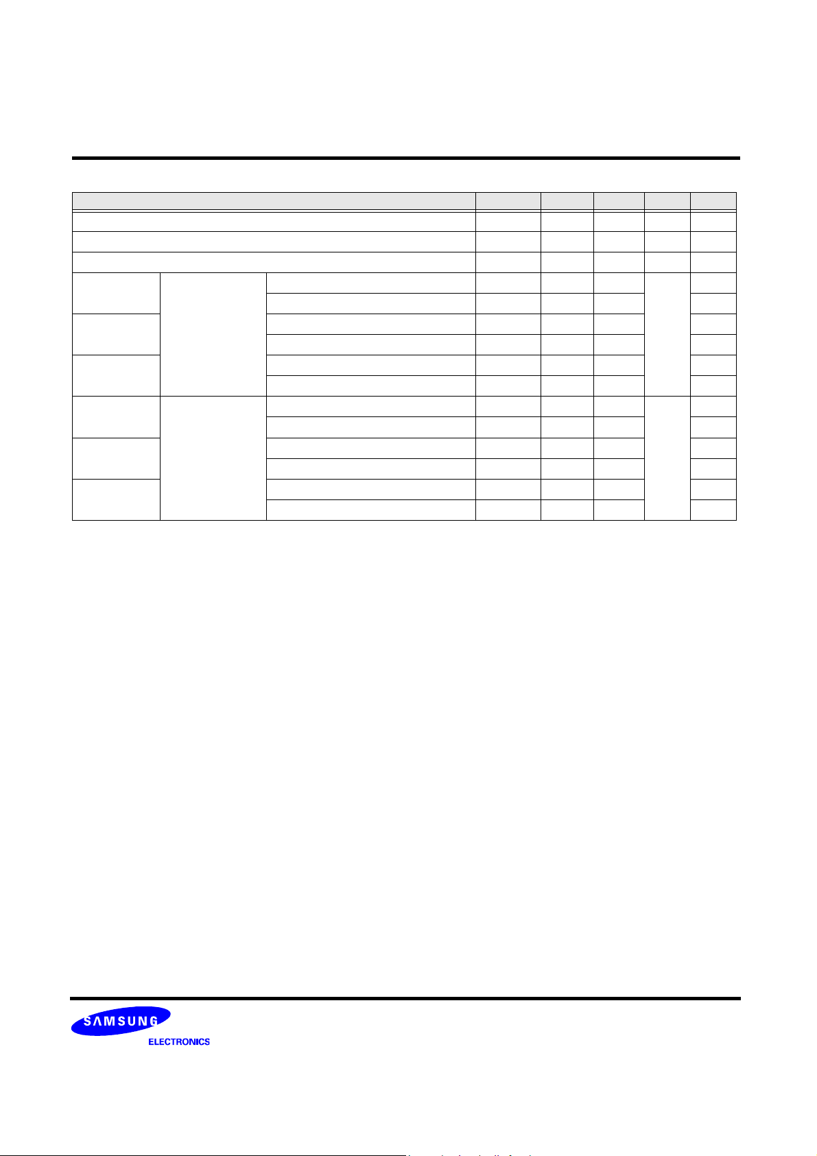
FEATURES
Parameter
CL = 4 4.0 ns 4.5 ns 5.0 ns
t
Clock Cycle Time (min)
CK
Random Read/Write Cycle Time (min)
t
RC
Random Access Time (min)
t
RAC
Operating Current (single bank) (max)
I
DD1S
Power Down Current (max)
I
DD2P
• Fully Synchronous Operation
- Double Data Rate (DDR)
- Data input/output are synchronized with both edges of DS / QS.
- Differential Clock (CLK and CLK
- CS
- Output data (DQs and QS) is aligned to the crossings of CLK and CLK
• Fast clock cycle time of 3.0 ns minimum
- Clock : 333 MHz maximum
- Data : 666 Mbps/pin maximum
• Quad Independent Banks operation
• Fast cycle and Short Latency
• Uni-directional Data Strobe
• Distributed Auto-Refresh cycle in 3.9us
• Power Down Mode
• Variable Write Length Control
• Write Latency = CAS
• Programable CAS
- CAS
- Burst Length = 4
• Organization : 4,194,304 words x 4 banks x 18 bits
• Power Supply Voltage V
• V
• 1.8V CMOS I/O comply with SSTL - 1.8 (half strength driver) and HSTL
• Package : 60Ball BGA, 1.0mm x 1.0mm Ball pitch
• Notice : Network-DRAM is trademark of Samsung Electronics., Co LTD
, FN and all address input signals are sampled on the positive edge of CLK.
Latency-1
Laatency = 4, 5, 6
Latency and Burst Length
: 2.5V ± 0.125V
DD
: 1.4V ∼ 1.9V
DDQ
) inputs
CL = 5 3.5 ns 3.75 ns 4.5 ns
CL = 6 3.0ns 3.33 ns 4.0 ns
F6 FB F5
20.0 ns 22.5 ns 25 ns
20.0 ns 22.5 ns 25 ns
320mA 300mA 280mA
70mA 65mA 60mA
K4C89183AF
.
- 4 -
REV. 0.7 Jan. 2005
K4C89183AF
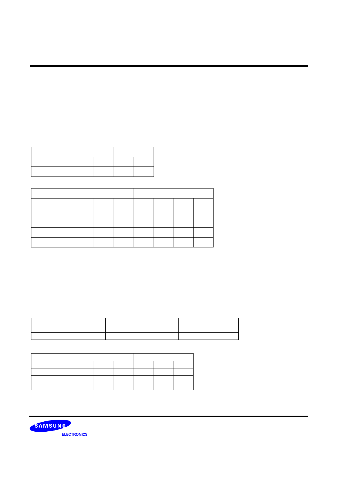
Pin Names
Pin Name
A0 ~ A14 Address Input
BA0, BA1 Bank Address
DQ0 ~ DQ17 Data Input/Output
CS
FN Function Control
PD
CLK, CLK
DS/QS Write/Read data strobe
VDD Power (+2.5V)
V
SS
V
DDQ
V
SSQ
V
REF
NC No Connection
Chip Select
Power Down Control
Clock Input
Ground
Power (+1.8V)
(for I/O buffer)
Ground
(for I/O buffer)
Reference Voltage
PIN ASSIGNMENT (TOP VIEW)
ball pitch=1.0 x 1.0mm
x18
123456
Index
V
A
DQ16
B
DQ15
C
DQ14
D
E
DQ12
F
DQ11
G
DQ10
H
DQ9
DQ17
ss
VssQ
VDDQ
DQ13
VssQ
VDDQ
VssQ
DS
DQ0
VDDQ
VssQ
DQ4
VDDQ
VssQ
VDDQ
QS
V
DD
DQ1
DQ2
DQ3
DQ5
DQ6
DQ7
DQ8
J
K
L
M
N
P
R
- 5 -
V
REF
CLK
A12
A11
A8
A5
V
SS
V
ss
CLK
PD
A9
A7
A6
A4
V
FN
CS
BA1
A0
A2
A3
DD
A14
A13
NC
BA0
A10
A1
V
DD
REV. 0.7 Jan. 2005
K4C89183AF
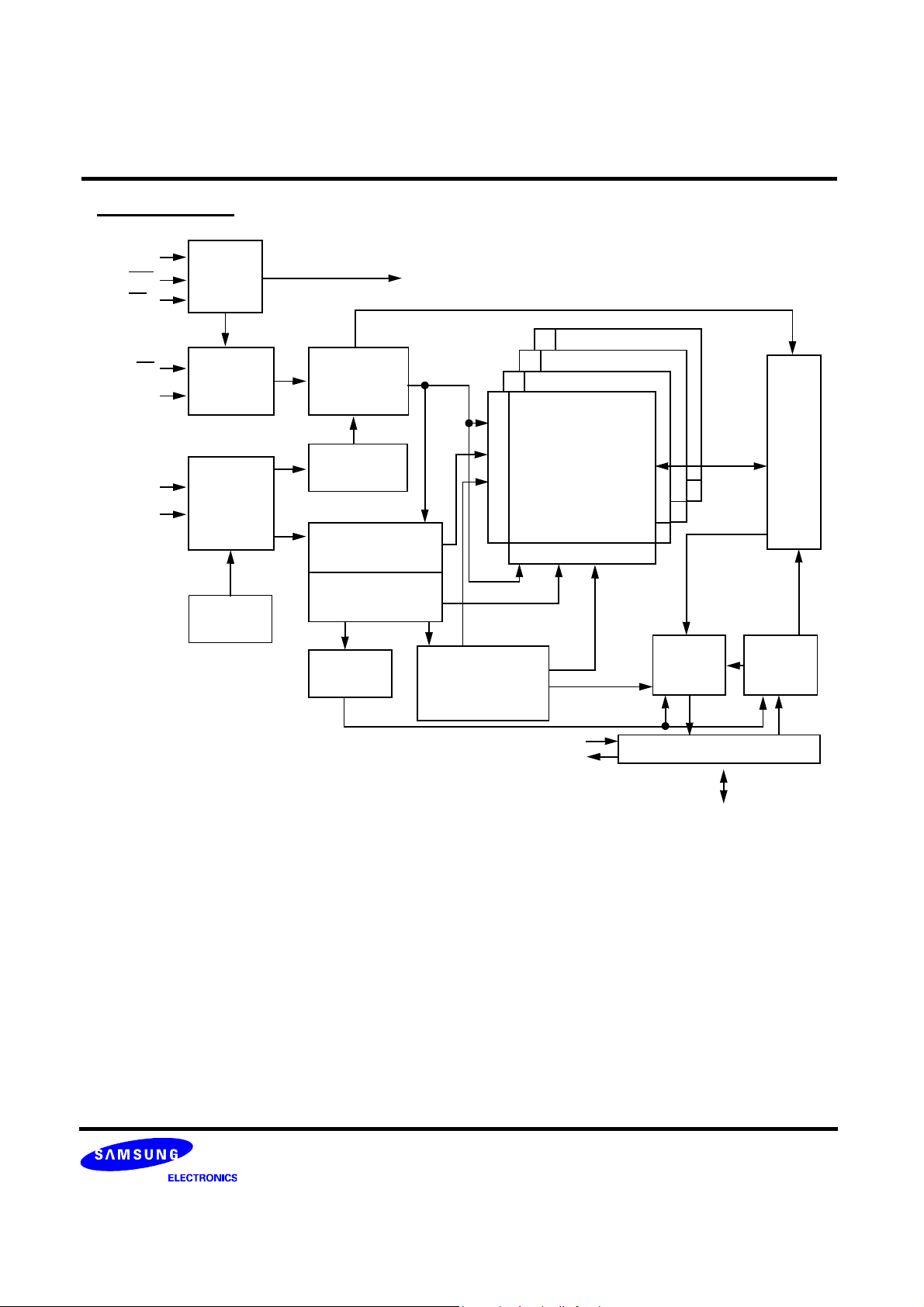
Block Diagram
CLK
CLK
PD
CS
FN
A0 ~ A14
BA0, BA1
DLL
CLOCK
BUFFER
COMMAND
DECODER
ADDRESS
BUFFER
REFRESH
COUNTER
To Each Block
CONTROL
SIGNAL
GENERATOR
MODE
REGISTER
UPPER ADDRESS
LATCH
LOWER ADDRESS
LATCH
BURST
COUNTER
ROW DECODER
COLUMN DECODER
WRITE ADDRESS
LATCH
ADDRESS
COMPARATOR
BANK #2
BANK #1
BANK #0
MEMORY
CELL
ARRAY
BANK #3
READ
DATA
BUFFER
DATA
WRITE
DATA
BUFFER
CIRCUIT
CONTROL AND LATCH
DS
QS
Note : The K4C89183AD configuration is 4 Bank of 32768 x 128 x 18 of cell array with the DQ pins numbered DQ0~DQ17.
- 6 -
DQ BUFFER
DQ0 ~ DQ17
REV. 0.7 Jan. 2005
K4C89183AF
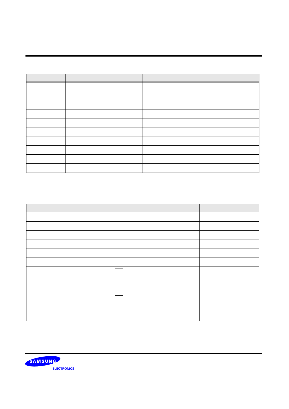
Absolute Maximum Ratings
Symbol Parameter Rating Units Notes
V
DD
V
DDQ
V
V
OUT
V
REF
T
OPR
T
STG
T
SOLDER
P
I
OUT
IN
D
Power Supply Voltage -0.3 ~ 3.3 V
Power Supply Voltage (for I/O buffer) -0.3 ~ VDD + 0.3 V
Input Voltage -0.3 ~ VDD + 0.3 V
DQ pin Voltage -0.3 ~ V
Input Reference Voltage -0.3 ~ V
+ 0.3 V
DDQ
+ 0.3 V
DDQ
Operating Temperature 0 ~ 85
Storage Temperature -55 ~ 150
Soldering Temperature(10s) 260
Power Dissipation 2 W
Short Circuit Output Current ± 50 mA
O
C
O
C
O
C
Case Temp.
Caution : Conditions outside the limits listed under "ABSOLUTE MAXIMUM RATINGS" may cause permanent damage to the device.
The device is not meant to be operated under conditions outside the limits described in the operational section of this specification. Exposure to "ABSOLUTE MAXIMUM RATINGS" conditions for extended periods may affect device reliability.
Recommended DC,AC Operating Conditions (Notes : 1) (Tcase = 0 ~ 85
O
C)
Symbol Parameter Min Typ Max Units Notes
V
DD
V
DDQ
V
REF
(DC) Input DC high Voltage V
V
IH
V
(DC) Input DC Low Voltage -0.1 - V
IL
(DC) Differential Clock DC Input Voltage -0.1 - V
V
ICK
V
(DC) Input Differential Voltage. CLK and CLK Inputs (DC) 0.4 - V
ID
(AC) Input AC High Voltage V
V
IH
V
(AC) Input AC Low Voltage -0.1 - V
IL
V
(AC) Input Differential Voltage. CLK and CLK Inputs (AC) 0.55 - V
ID
(AC) Differential AC Input Cross Point Voltage V
V
X
V
(AC) Differential Clock AC Middle Level V
ISO
Power Supply Voltage 2.375 2.5 2.625 V
Power Supply Voltage (for I/O Buffer) 1.7 1.8 1.9 V
Input Reference Voltage V
/2x95% V
DDQ
+0.125 - V
REF
+0.2 - V
REF
/2-0.125 - V
DDQ
/2-0.125 - V
DDQ
DDQ
/2 V
/2x105% V 2
DDQ
+0.2 V 5
DDQ
-0.125 V 5
REF
+0.1 V 10
DDQ
+0.2 V 7,10
DDQ
+0.2 V 3,6
DDQ
-0.2 V 4,6
REF
+0.2 V 7,10
DDQ
/2+0.125 V 8,10
DDQ
/2+0.125 V 9,10
DDQ
- 7 -
REV. 0.7 Jan. 2005
K4C89183AF
1. All voltages are referenced to Vss, VssQ.
Notes
:
2. V
Peak to peak AC noise on V
3. Overshoot Iimit : V
4. Undershoot Iimit : V
5. V
6. V
7. V
8. The value of Vx(AC) is expected to equal VddQ/2 of the transmitting device.
9. V
10. Refer to the figure below.
is expected to track variations in VddQ DC level of the transmitting device.
REF
(DC) and VIL(DC) are levels to maintain the current logic state.
IH
(AC) and VIL(AC) are levels to change to the new logic state.
IH
is magnitude of the difference between CLK input level and CLK input level.
ID
means [V
ISO
CLK
CLK
V
SS
VID(AC)
0 V Differential
may not exceed ± 2% of V
REF
(max.) = VddQ + 0.7V with a pulse width <= 5ns
IH
(min.) = -0.7V with a pulse width <= 5ns
IL
(CLK) + V
ICK
V
ICK
V
X
(CLK)]/2
ICK
V
X
V
ICK
V
(DC).
REF
X
V
X
V
ICK
V
X
V
ICK
VID(AC)
V
ISO
V
SS
11. In the case of external termination, VTT(Termination Voltage) should be gone in the range of V
Pin Capacitance (V
= 2.5V, V
DD
V
(min)
ISO
= 1.8V, f = 1 MHz, Ta = 25oC)
DDQ
V
(max)
ISO
(DC) ± 0.04V.
REF
Symbol Parameter Min Max Delts Units
C
IN
C
INC
C
I/O
C
NC
Input Pin Capacitance 1.5 3.0 0.25 pF
Clock Pin (CLK, CLK) Capacitance 1.5 3.0 0.25 pF
DQ, DS, QS Capacitance 2.5 3.5 0.5 pF
NC Pin Capacitance - 1.5 - pF
Note : These parameters are periodically sampled and not 100% tested.
- 8 -
REV. 0.7 Jan. 2005
K4C89183AF
DC Characteristics and Operating Conditions (VDD = 2.5V ± 0.125V, VDDQ = 1.8V ± 0.1V, Tcase = 0~85 °C)
Parameter Symbol
Operating Current
One bank Read or Write operation;
t
= min, I
CK
RC
= min, I
OUT
= 0mA;
Burst Length = 4, CAS Latency = 6, Free running QS mode;
0V ≤ V
IN
≤ V
IL(AC)
(max.), V
IH(AC)
(min.) ≤ V
IN
≤ V
DDQ;
Address inputs change up to 2 times during minimum IRC,
Read data change twice per clock cycle
Standby Current
All Banks : inactive state;
t
=min, CS = VIH, PD = VIH;
CK
0V ≤ V
Other input signals change one time during 4*t
≤ VIL(AC)(max.), VIH(AC)(min.) ≤ V
IN
IH
≤ V
CK,
DDQ;
DQ and DS inputs change twice per clock cycle
Standby (Power Down) Current
All Banks : inactive state;
t
=min, PD = VIL (Power Down);
CK
CAS Latency = 6, Free running QS mode;
0V ≤ V
Other input signals change one time during 4*t
DQ and DS inputs are floating(V
≤ VIL(AC)(max), VIH(AC)(min) ≤ V
IN
DDQ
/2)
IN
≤ V
CK
DDQ
,
;
Write Operating Current(4 Banks)
4 Bank intereaved continuous burst write operation;
t
= min, I
CK
RC
= min;
Burst Length = 4, CAS Latency = 6, Free running QS mode;
0V ≤ V
≤ VIL(AC) (max.), VIH(AC)(min.) ≤ V
IN
IN
≤ V
DDQ;
Address inputs change once per clock cycle,
DQ and DS inputs change twice per clock cycle
Read Operating Current(4 Banks)
4 Bank intereaved continuous burst write operation;
t
= min, I
CK
RC
= min, I
OUT
= 0mA;
Burst Length = 4, CAS Latency = 6, Free running QS mode;
0V ≤ V
≤ VIL(AC) (max.), VIH(AC)(min.) ≤ V
IN
IN
≤ V
DDQ;
Address inputs change once per clock cycle,
Read data change twice per clock cycle
Burst Auto-Refresh Current
Refresh command at every I
t
= min, I
CK
REFC
= min;
REFC
interval;
CAS Latency = 6, Free running QS mode;
0V ≤ V
Address change up to 2 times during minimum I
≤ VIL(AC) (max.), VIH(AC) (min.) ≤ V
IN
IN
≤ V
REFC
DDQ;
,
DQ and DS inputs change twice per clock cycle
I
DD1S
I
DD2N
I
DD2P
I
DD4W
I
DD4R
I
DD5B
Max
F6 FB F5
320 300 280
Units Notes
1, 2
100 95 90 1
70 65 60 1
mA
650 600 550 1
650 600 550 1,2
250 235 210 1,3
- 9 -
REV. 0.7 Jan. 2005
K4C89183AF
DC Characteristics and Operating Conditions (VDD = 2.5V ± 0.125V , VDDQ = 1.8V ± 0.1V, Tcase = 0~85 °C)
Parameter Symbol Min Max Unit Notes
Input Leakage Current (0V<=V
Output Leakage Current (Output disabled, 0V<=V
Current I
V
REF
Normal Output
Driver
Strong Output
Driver
Output DC Current
(V
= 1.7 ~ 1.9V)
DDQ
Weak Output
Driver
Normal Output
Driver
Strong Output
Driver
Output DC Current
(V
= 1.4 ~ 1.6V)
DDQ
Weak Output
Driver
Notes : 1. These parameters depend on the cycle rate and these values are measured at a cycle rate with the minimum values of
t
, tRC and IRC.
CK
2. These parameters depend on the output loading. The specified values are obtained with the output open.
3. I
is specified under burst refresh condition. Actual system should use distributed refresh that meet to t
DD5B
4. Refer to output driver characteristics for the detail. Output Driver Strength is selected by Extended Mode Register.
<=VddQ, All other pins not under test = 0V) I
IN
<=VddQ) I
OUT
= 1.420V IOH(DC)
V
OH
= 0.280V IOL(DC)
V
OL
= 1.420V IOH(DC)
V
OH
= 0.280V IOL(DC)
V
OL
= 1.420V IOH(DC)
V
OH
= 0.280V IOL(DC)
V
OL
V
= V
OH
V
V
OH
V
- 0.4 IOH(DC)
DDQ
= 0.4V IOL(DC)
OL
= V
- 0.4 IOH(DC)
DDQ
= 0.4V IOL(DC)
OL
Not defined
Not defined
LI
LO
REF
-5 5 uA
-5 5 uA
-5 5 uA
-5.6 -
5.6 - 4
-9.8 - 4
9.8 - 4
mA
-2.8 - 4
2.8 -
-4 -
-4 - 3
-8 - 3
-8 - 3
(DC)
I
OH
(DC)
I
OL
--
--
mA
specification
REFI
4
3
- 10 -
REV. 0.7 Jan. 2005
K4C89183AF
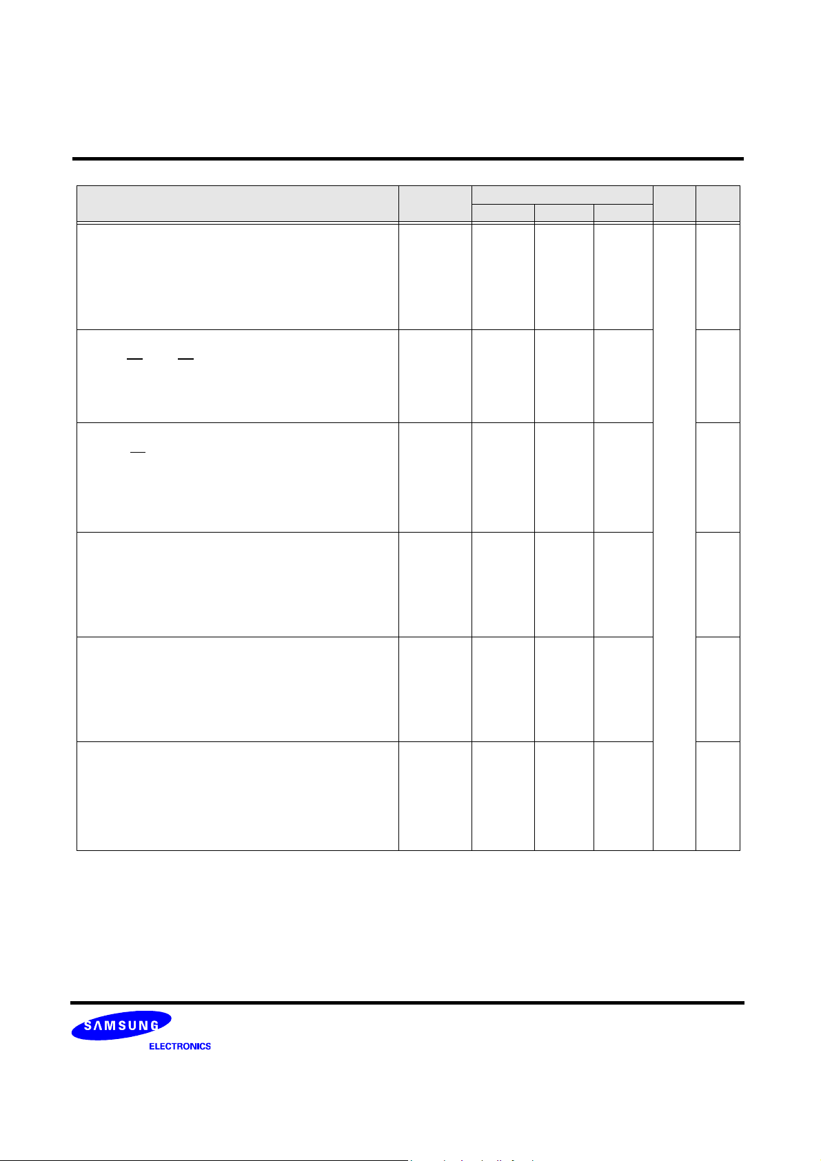
AC Characteristics and Operating Conditions (Notes : 1, 2)
Symbol Parameter
t
RC
t
CK
t
RAC
t
CH
t
CL
t
CKQS
t
QSQ
t
AC
t
OH
t
HP
t
QSP
t
QSQV
t
QHS
t
DQSS
t
DSPRE
t
DSPRES
t
DSPREH
t
DSP
t
DSS
t
DSPST
t
DSPSTH
t
DS
t
DH
t
IS
t
IH
Random Cycle Time 20.0 - 22.5 - 25 -
Clock Cycle Time
Random Access Time - 20.0 - 22.5 - 25 3
Clock High Time
Clock Low Time
QS Access Time from CLK -0.45 0.45 -0.45 0.45 -0.5 0.5 3, 8
Data Output Skew from QS - 0.2 - 0.25 - 0.3 4
Data Access Time from CLK -0.5 0.5 -0.5 0.5 -0.6 0.6 3, 8
Data Output Hold Time from CLK -0.5 0.5 -0.5 0.5 -0.6 0.6 3, 8
CLK half period ( minium of Actual tCH, tCL)
QS(Read) Pulse Width
Data Output Valid Time from QS
DQ, QS Hold skew factor -
DS(Write) Low to High Setup Time
DS(Write) Preamble Pulse Width
DS First Input Setup Time 0 - 0 - 0 - 3
DS First Low Input Hold Time
DS High or Low Input Pulse Width
DS Input Falling Edge to Clock Setup
Time
DS(Write) Postamble Pulse Width
DS(Write) Postamble Hold Time
Data Input Setup Time from DS 0.3 - 0.35 - 0.4 - 4
Data Input Hold Time from DS 0.3 - 0.35 - 0.4 - 4
Command / Address Input Setup Time 0.6 - 0.6 - 0.7 - 3
Command / Address Input Hold Time 0.6 - 0.6 - 0.7 - 3
F6 FB F5
Min Max Min Max Min Max
Units Notes
3
= 4
C
L
C
L
C
L
C
L
C
L
C
L
C
L
C
L
C
L
C
L
C
L
4.0 6.0 4.5 6.0 5.0 6.0 3
= 5
3.33 6.0 3.75 6.0 4.5 6.0 3
= 6
3.0 6.0 3.33 6.0 4.0 6.0 3
0.45*t
CK
0.45*t
CK
min(t
,
CH
t
)
CL
t
HP-tQHS
t
HP-tQHS
0.055x
t
CK
0.8*t
0.4*t
0.3*t
0.45*t
= 4
0.75 - 0.8 - 1.0 - 3, 4
= 5
0.75 - 0.8 - 1.0 - 3, 4
= 6
0.75 - 0.8 - 1.0 - 3, 4
= 7
0.45*t
= 4
0.75 - 0.8 - 1.0 - 3, 4
= 5
0.75 - 0.8 - 1.0 - 3, 4
= 6
0.75 - 0.8 - 1.0 3, 4
= 7
1.2*t
CK
CK
CK
0.55*tCK0.45*tCK0.55*tCK0.45*tCK0.55*t
CK
------ 3, 4
CK
------ 3, 4
-
-
-
-
-
+0.17
CK
-
-
-
0.45*t
0.45*t
min(t
t
CL
t
HP-tQHS
t
HP-tQHS
-
0.8*t
0.4*t
0.3*t
0.45*t
0.45*t
-
CK
0.45*t
-
CK
,
CH
)
0.055x
t
CK
1.2*t
CK
CK
CK
CK
-
-
-
+0.17
CK
-
-
min(t
t
CL
t
HP-tQHS
t
HP-tQHS
-
0.8*t
0.4*t
0.3*t
0.45*t
CH
)
CK
CK
CK
-3
CK
-3
CK
,
-3
-4, 8
-4, 8
0.055x
t
+0.17
CK
1.2*t
-4
-3
-4
CK
CK
CK
3
ns
4
- 11 -
REV. 0.7 Jan. 2005
K4C89183AF
AC Characteristics and Operating Conditions (Notes : 1, 2) (Continued)
Symbol Parameter
t
t
t
t
t
t
t
t
I
I
I
I
I
I
I
I
I
I
I
I
Data-out Low Impedance Time from CLK -0 .5 - -0.5 - -0.6 - 3, 6, 8
LZ
Data-out High Impedance Time from CLK - 0.5 - 0.5 - 0.6 3, 7, 8
HZ
Last Output to PD High Hold Time 0 - 0 - 0 -
QPDH
Power Down Exit Time 0.6 - 0.6 - 0.7 - 3
PDEX
Input Transition Time 0.1 1 0.1 1 0.1 1
T
PD Low Input Window for Self-Refresh Entry
FPDL
Auto-Refresh Aver age Interval 0.4 3.9 0.4 3.9 0.4 3.9
REFI
Pause Time after Power-up 200 - 200 - 200 -
PAUSE
Random Read/Write Cycle Time
RC
(Applicable to Same Bank)
RDA/WRA to LAL Command Input Delay
RCD
(Applicable to Same Bank)
LAL to RDA/WRA Command Input Delay
RAS
(Applicable to Same Bank)
Random Bank Access Delay
RBD
(Applicable to Other Bank)
LAL following RDA to WRA Delay
RWD
(Applicable to Other Bank)
LAL following WRA to RDA Delay
WRD
(Applicable to Other Bank)
Mode Register Set Cycle T ime
RSC
PD Low to Inactive State of Input Buffer - 2 - 2 - 2
PD
PD High to Active State of Input Buffer 1 - 1 - 1 -
PDA
Power down mode valid from REF com-
PDV
mand
Auto-Refresh Cycle Time
REFC
DLL Lock-on Time (Applicable to RDA command) 200 - 200 - 200 -
LOCK
F6 FB F5
Min Max Min Max Min Max
-0.5*t
CK
= 4
C
L
C
= 5
L
C
= 6
L
C
= 7
L
= 4
C
L
C
= 5
L
C
= 6
L
= 7
C
L
BL = 4 3 - 3 - 3 -
= 4
C
L
C
= 5
L
C
= 6
L
C
= 7
L
= 4
C
L
C
= 5
L
C
= 6
L
= 7
C
L
= 4
C
L
C
= 5
L
C
= 6
L
C
= 7
L
5-5-56-6-67-7-7-
------
111111
4-4-45-5-56-6-6-
------
2-2-2-
1-1-1-
7-7-77-7-77-7-7-
19 - 19 - 19 23 - 23 - 23 25 - 25 - 25 -
19 - 19 - 19 23 - 23 - 23 25 - 25 - 25 -
-0.5*t
5
CK
-0.5*t
5
CK
Units Notes
53
5
us
Cycle
- 12 -
REV. 0.7 Jan. 2005
K4C89183AF
AC Test Conditions
Symbol Parameter Value Units Notes
(min)
V
V
IL
V
V
IH
(max)
V
REF
V
TT
SWING
V
(AC)
ID
Input high voltage (minimum)
Input low voltage (maximum)
Input reference voltage VddQ/2 V
Termination voltage
Input signal peak to peak swing 0.7 V
Differential clock input reference level
R
Input differential voltage 1.0 V
SLEW Input signal minimum slew rate 2.5 V/ns
V
OTR
Output timing measurement reference voltage VddQ/2 V 9
VddQ
VIH min
(AC)
V
V
REF
REF
V
V
REF
X(AC)
+ 0.2
- 0.2
V
V
V
V
V
TT
V
SWING
V
REF
VIL max
(AC)
Output
25 Ω
Measurement Point
Vss
∆T ∆T
Slew=(VIHmin
(AC)
- VILmax
(AC)
)/∆T
Notes : 1. Transition times are measured between VIH min
and VIL max
(DC)
(DC)
.
AC Test Load
Transition (rise and fall) of input signals have a fixed slope.
2. If the result of nominal calculation with regard to t
contains more than
CK
one decimal place, the result is rounded up to the nearest decimal place.
(i.e., t
3. These parameters are measured from the differential clock (CLK and CLK
4. These parameters are measured from signal transition point of DS crossing V
5. The t
The t
= 0.8*tCK, tCK = 3.3ns, 0.8*3.3 ns = 2.64 ns is rounded up to 2.7 ns.)
DQSS
) AC cross point.
(MAX.) applies to equally distributed refresh method.
REFI
(MIN.) applies to both burst refresh method and distributed refresh method.
REFI
REF
level.
In such case, the average interval of eight consecutive Auto-Refresh commands has to be more than 400ns always. In
other words, the number of Auto- Refresh cycles which can be performed within 3.2us (8X400ns) is to 8 times in the
maximum.
6. Low Impedance State is speified at VddQ/2± 0.2V from steady state.
7. High Impedance State is specified where output buffer is no longer driven.
8. These parameters depend on the clock jitter. These parameters are measured at stable clock.
9. Output timing is measured by using Normal driver strength at V
Output timing is measured by using S trong driver strength at V
= 1.7V ~ 1.9V.
DDQ
= 1.4V ~ 1.6V
DDQ
- 13 -
REV. 0.7 Jan. 2005
K4C89183AF
Power Up Sequence
1. As for PD, being maintained by the low state (<0.2V) is desirable before a power-supply injection.
2. Apply V
3. Apply V
4. Start clock (CLK, CLK
5. After stable power and clock, apply DESL and take PD
6. Issue EMRS to enable DLL and to define driver strength and data strobe type. (Note : 1)
7. Issue MRS for set CAS
8. Issue two or more Auto-Refresh commands. (Note:1)
9. Ready for normal operation after 200 clocks from Extended Mode Register programming.
Note : 1. Sequence 6, 7 and 8 can be issued in random order.
2. L=Logic Low, H = Logic High
before or at the same time as V
DD
before or at the same time as V
DDQ
) and maintain stable condition for 200us (min.).
Latency (CL), Burst Type (BT), and Burst Length (BL). (Note : 1)
V
DD
V
DDQ
V
REF
∼
∼
∼
∼
∼
∼
DDQ
2.5V(TYP)
1.8V(TYP)
0.9V(TYP)
REF
.
.
= H.
∼
∼
∼
∼
∼
∼
∼
∼
∼
∼
∼
∼
∼
∼
∼
∼
∼
∼
∼
∼
∼
∼
∼
∼
CLK
CLK
PD
Command
Address
DQ
DS
QS
(Uni-QS mode)
(Free Running mode)
QS
200 µs(min)
Hi-Z
∼
∼
t
PDEX
I
PDA
∼
∼
∼
∼
DESL RDA MRS DESL RDA MRS DESL WRA REF WRA REFDESL DESL
∼
∼
∼
∼
∼
∼
EMRS MRS
∼
∼
l
RSC
∼
∼
∼
∼
op-code op-code
∼
∼
∼
∼
∼
∼
∼
∼
∼
∼
EMRS
∼
∼
∼
∼
∼
∼
∼
∼
MRS Auto Refresh cycle Normal Operation
∼
l
RSC
∼
∼
∼
∼
∼
∼
∼
∼
∼
l
REFC
∼
∼
200 clock cycle(min)
∼
∼
∼
∼
∼
∼
∼
∼
∼
∼
∼
∼
l
REFC
∼
∼
∼
∼
∼
∼
∼
∼
∼
∼
∼
∼
∼
∼
Low
∼
∼
- 14 -
REV. 0.7 Jan. 2005
K4C89183AF
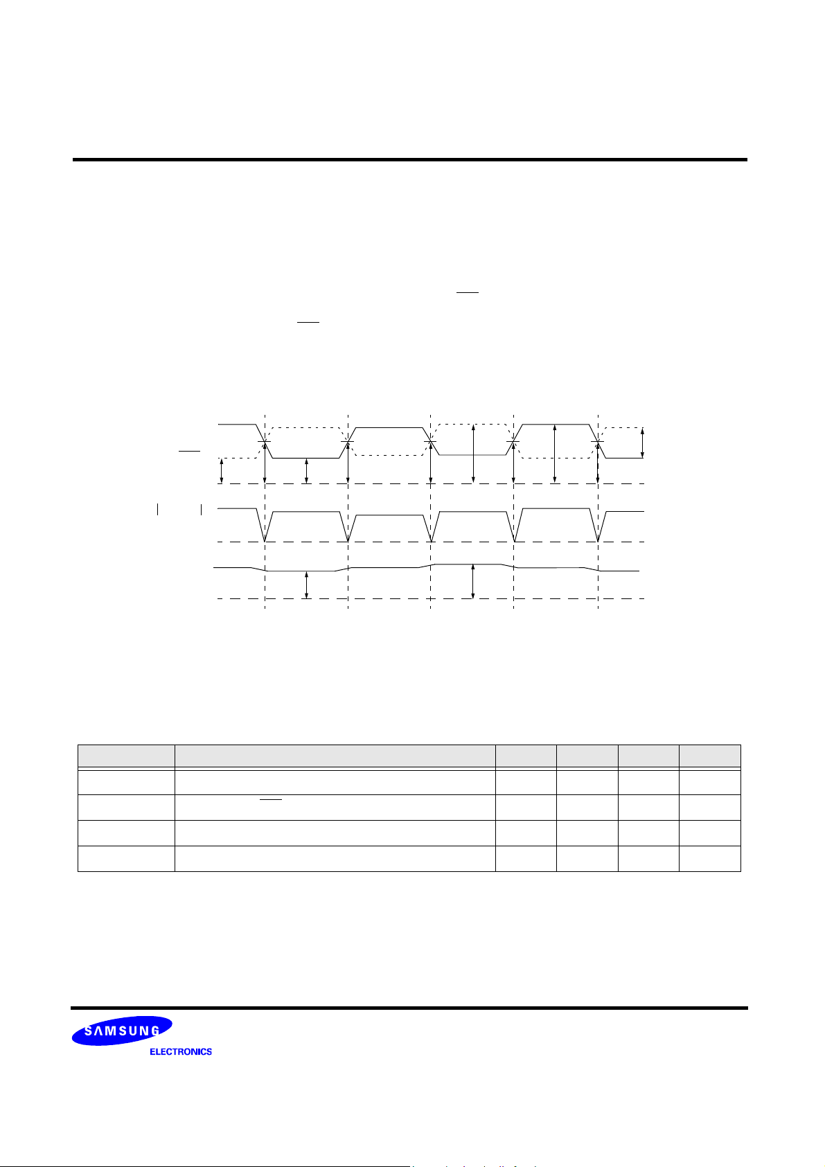
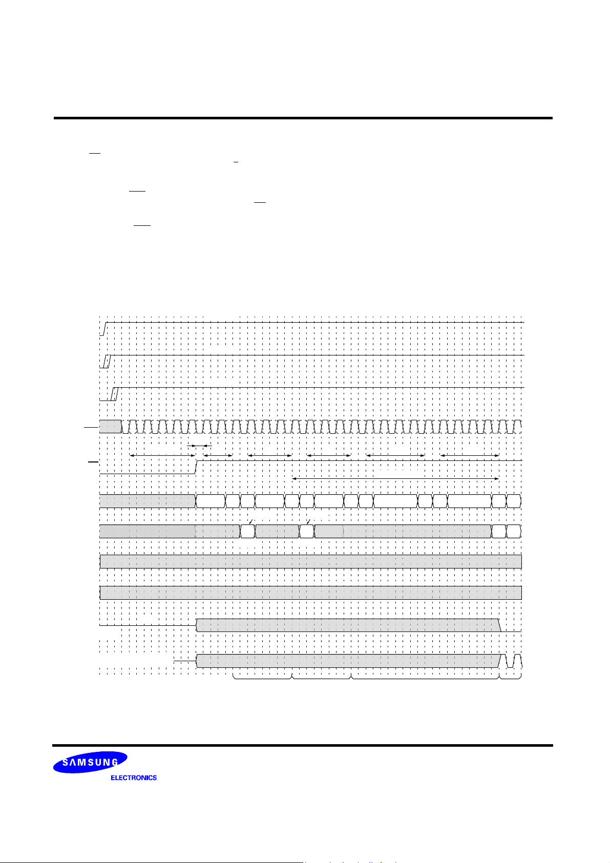
Basic Timing Diagrams
Input Timing
Command and Address
CK
CK
t
t
CK
CK
~
~
t
CH
t
CL
CS
FN
A0-A14
BA0.BA1
Data
DS
DQn (Input)
DQm (Input)
t
IS
t
IS
t
IS
1st
1st
UA, BA
t
DS
t
DS
t
IPW
t
IH
t
IH
t
IH
t
DH
t
DH
t
IS
t
IS
t
IS
t
DStDH
t
DStDH
2nd
2nd
LA
t
t
t
IPW
t
~
IH
IH
IH
~
~
~
~
~
~
~
~
~
~
~
~
~
~
~
~
~
~
~
~
~
Refer to the Command Truth Table.
Timing of the CLK, CLK
CLK
CLK
CLK
CLK
t
CH
t
CK
V
X
V
X
- 15 -
t
CL
V
IH
V
IH(AC)
V
IL(AC)
V
t
T
t
T
V
X
IL
V
IH
V
V
IL
ID(AC)
REV. 0.7 Jan. 2005

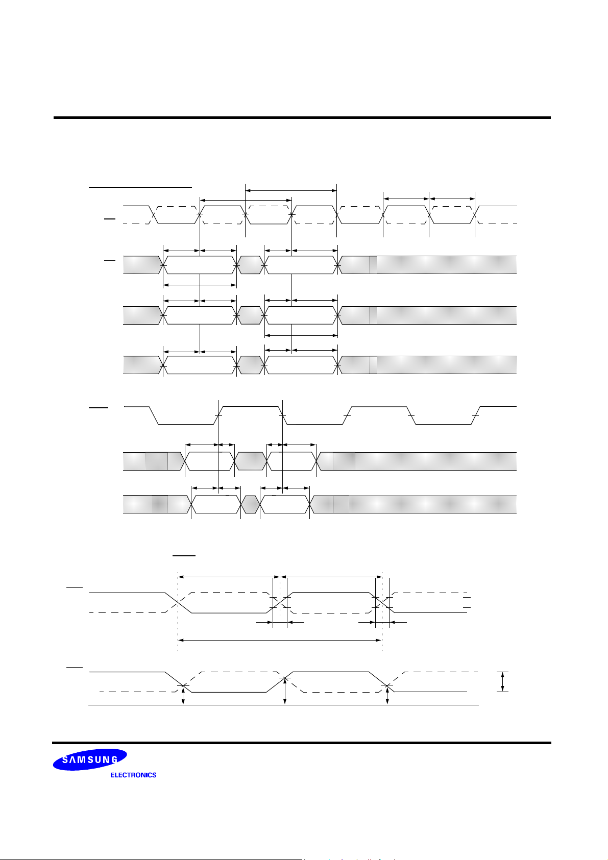
K4C89183AF
Read Timing (Burst Length = 4)
Unidirectional DS/QS mode
CK
CK
Input
(Control &
Addresses)
LDS/UDS
(Input)
CAS
latency = 4
LQS/UQS
(Output)
DQ
(Output)
0123456789101112131415161718
tISt
t
CHtCL
IH
LAL
Low
High-Z
t
(after RDA)
CK
DESL
t
CKQS
t
CKQS
t
LZ
t
QSQ
Q0
t
AC
t
CKQS
t
QSPtQSP
t
QSQV
t
t
QSQ
QSQV
Q1 Q2 Q3
t
ACtAC
t
QSQ
Low
t
HZ
t
OH
CAS latency = 5
LQS/UQS
(Output)
DQ
(Output)
CAS latency = 6
LQS/UQS
(Output)
DQ
(Output)
Note : DQ0 to DQ17 are aligned with LQS.
DQ18 to DQ35 are aligned with UQS.
Low
High-Z
Low
High-Z
t
CKQS
t
CKQS
t
LZ
t
QSQ
Q0
t
AC
t
CKQS
t
QSPtQSP
t
QSQV
t
t
QSQ
QSQV
Q1 Q2 Q3
t
ACtAC
t
CKQS
t
CKQS
t
LZ
t
QSQ
Q0
t
AC
t
QSQ
t
HZ
t
OH
t
CKQS
t
QSPtQSP
t
QSQV
t
t
QSQ
QSQV
Q1 Q2 Q3
t
ACtAC
Low
t
QSQ
Low
t
HZ
t
OH
- 16 -
REV. 0.7 Jan. 2005
K4C89183AF
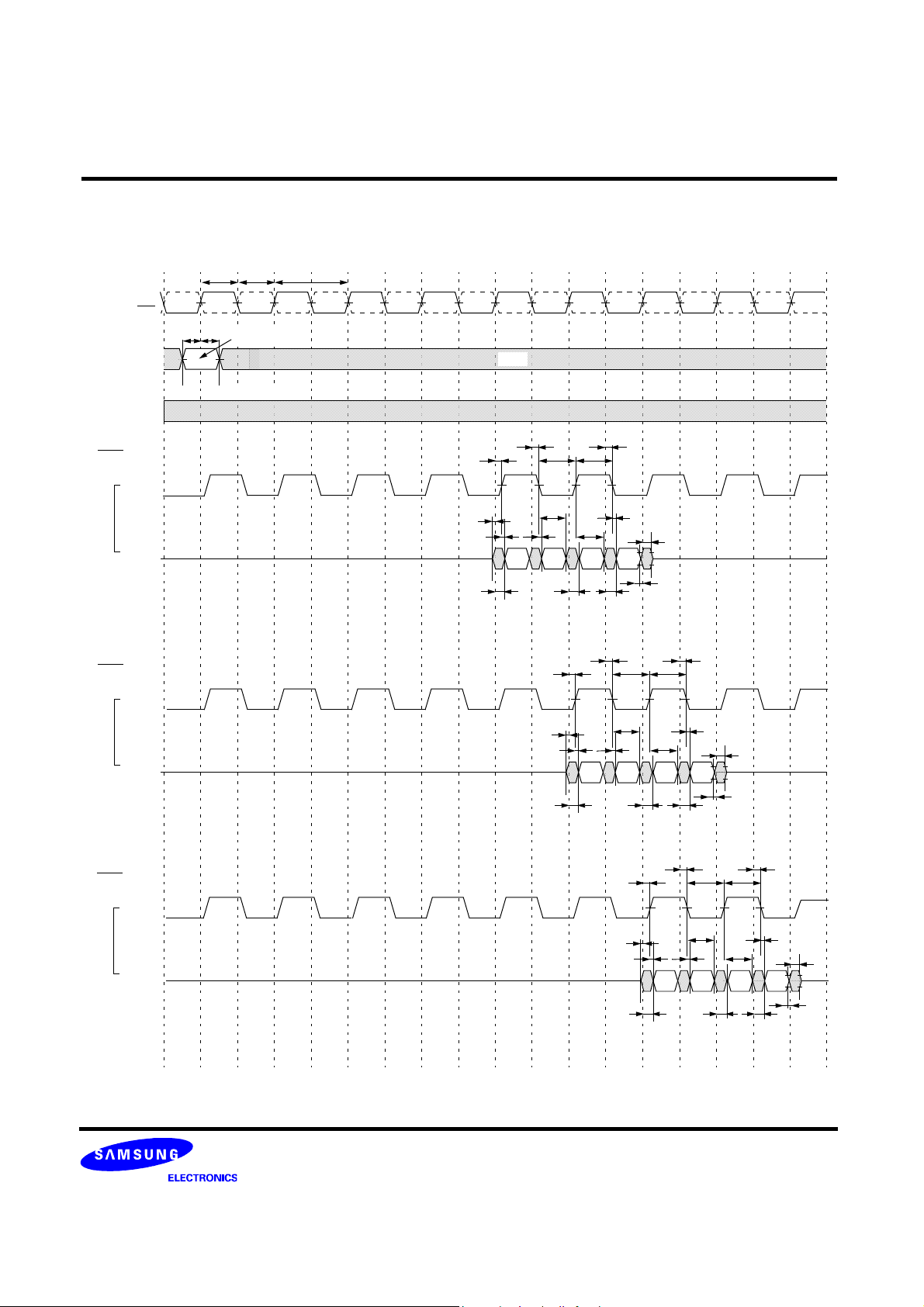
Read Timing (Burst Length = 4)
Unidirectional DS/Free Running QS mode
CK
CK
Input
(Control &
Addresses)
LDS/UDS
(Input)
CAS
latency = 4
LQS/UQS
(Output)
DQ
(Output)
0123456789101112131415161718
tISt
t
CHtCL
IH
LAL
High-Z
(after RDA)
t
CK
DESL
t
CKQS
t
CKQS
t
LZ
t
QSQ
Q0
t
AC
t
CKQS
t
QSPtQSP
t
QSQV
t
t
QSQ
QSQV
Q1 Q2 Q3
t
ACtAC
t
QSQ
t
HZ
t
OH
CAS latency = 5
LQS/UQS
(Output)
DQ
(Output)
CAS latency = 6
LQS/UQS
(Output)
DQ
(Output)
Note : DQ0 to DQ17 are aligned with LQS.
DQ18 to DQ35 are aligned with UQS.
High-Z
High-Z
LQS/UQS is always asserted in Free Running QS mode.
t
CKQS
t
CKQS
t
LZ
t
QSQ
Q0
t
AC
t
CKQS
t
QSPtQSP
t
QSQV
t
t
QSQ
QSQV
Q1 Q2 Q3
t
ACtAC
t
CKQS
t
CKQS
t
LZ
t
QSQ
Q0
t
AC
t
QSQ
t
HZ
t
OH
t
CKQS
t
QSPtQSP
t
QSQV
t
t
QSQ
QSQV
Q1 Q2 Q3
t
ACtAC
t
QSQ
t
HZ
t
OH
- 17 -
REV. 0.7 Jan. 2005
 Loading...