


2Gb C-die DDR3 SDRAM
http://www.BDTIC.com/SAMSUNG
78FBGA with Lead-Free & Halogen-Free
(RoHS compliant)
Rev. 1.31, Nov. 2010
K4B2G0446C
K4B2G0846C
datasheet
SAMSUNG ELECTRONICS RESERVES THE RIGHT TO CHANGE PRODUCTS, INFORMATION AND
SPECIFICATIONS WITHOUT NOTICE.
Products and specifications discussed herein are for reference purposes only. All information discussed
herein is provided on an "AS IS" basis, without warranties of any kind.
This document and all information discussed herein remain the sole and exclusive property of Samsung
Electronics. No license of any patent, copyright, mask work, trademark or any other intellectual property
right is granted by one party to the other party under this document, by implication, estoppel or otherwise.
Samsung products are not intended for use in life support, critical care, medical, safety equipment, or
similar applications where product failure could result in loss of life or personal or physical harm, or any
military or defense application, or any governmental procurement to which special terms or provisions
may apply.
For updates or additional information about Samsung products, contact your nearest Samsung office.
All brand names, trademarks and registered trademarks belong to their respective owners.
ⓒ 2010 Samsung Electronics Co., Ltd. All rights reserved.
- 1 -
K4B2G0446C
http://www.BDTIC.com/SAMSUNG
K4B2G0846C
datasheet DDR3 SDRAM
Revision History
Revision No. History Draft Date Remark Editor
1.0 - First Release Dec. 2009 - S.H.Kim
1.01 - Corrected Current Data Dec. 2009 - S.H.Kim
1.1 - Deleted operation frequency of DDR3 800 (6-6-6) Jan. 2010 - S.H.Kim
1.2 - Added "CL5" to supported CL setting Feb. 2010 - S.H.Kim
1.21 - Corrected Typo. Feb. 2010 - S.H.Kim
1.22 - Corrected Typo. Apr. 2010 - S.H.Kim
1.3 - Updated JESD79-3E Jun. 2010 - S.H.Kim
1.31 - Corrected Typo. Nov. 2010 - S.H.Kim
Rev. 1.31
- 2 -

K4B2G0446C
http://www.BDTIC.com/SAMSUNG
K4B2G0846C
datasheet DDR3 SDRAM
Table Of Contents
2Gb C-die DDR3 SDRAM
1. Ordering Information .....................................................................................................................................................5
2. Key Features................................................................................................................................................................. 5
3. Package pinout/Mechanical Dimension & Addressing................................................................................................. 6
3.1 x4 Package Pinout (Top view) : 78ball FBGA Package .......................................................................................... 6
3.2 x8 Package Pinout (Top view) : 78ball FBGA Package .......................................................................................... 7
3.3 FBGA Package Dimension (x4/x8).......................................................................................................................... 8
4. Input/Output Functional Description..............................................................................................................................9
5. DDR3 SDRAM Addressing ...........................................................................................................................................10
6. Absolute Maximum Ratings ..........................................................................................................................................11
6.1 Absolute Maximum DC Ratings............................................................................................................................... 11
6.2 DRAM Component Operating Temperature Range ................................................................................................ 11
7. AC & DC Operating Conditions..................................................................................................................................... 11
7.1 Recommended DC operating Conditions (SSTL_1.5)............................................................................................. 11
8. AC & DC Input Measurement Levels ............................................................................................................................12
8.1 AC & DC Logic input levels for single-ended signals .............................................................................................. 12
8.2 V
8.3 AC & DC Logic Input Levels for Differential Signals...............................................................................................14
8.4 Differential Input Cross Point Voltage...................................................................................................................... 16
8.5 Slew rate definition for Differential Input Signals .....................................................................................................16
8.6 Slew rate definitions for Differential Input Signals ................................................................................................... 16
9. AC & DC Output Measurement Levels ......................................................................................................................... 17
9.1 Single-ended AC & DC Output Levels..................................................................................................................... 17
9.2 Differential AC & DC Output Levels......................................................................................................................... 17
9.3 Single-ended Output Slew Rate .............................................................................................................................. 17
9.4 Differential Output Slew Rate .................................................................................................................................. 18
9.5 Reference Load for AC Timing and Output Slew Rate ............................................................................................ 18
9.6 Overshoot/Undershoot Specification ....................................................................................................................... 19
9.7 34ohm Output Driver DC Electrical Characteristics.................................................................................................20
9.8 On-Die Termination (ODT) Levels and I-V Characteristics ..................................................................................... 21
9.9 ODT Timing Definitions ........................................................................................................................................... 24
10. IDD Current Measure Method..................................................................................................................................... 27
10.1 IDD Measurement Conditions ...............................................................................................................................27
11. 2Gb DDR3 SDRAM C-die IDD Specification Table ....................................................................................................36
12. Input/Output Capacitance ...........................................................................................................................................37
13. Electrical Characteristics and AC timing for DDR3-800 to DDR3-1600 ...................................................................... 38
13.1 Clock Specification ................................................................................................................................................ 38
13.2 Refresh Parameters by Device Density................................................................................................................. 39
13.3 Speed Bins and CL, tRCD, tRP, tRC and tRAS for corresponding Bin ................................................................. 39
Tolerances...................................................................................................................................................... 13
REF
8.3.1. Differential signals definition ............................................................................................................................ 14
8.3.2. Differential swing requirement for clock (CK - CK
8.3.3. Single-ended requirements for differential signals ...........................................................................................15
9.6.1. Address and Control Overshoot and Undershoot specifications...................................................................... 19
9.6.2. Clock, Data, Strobe and Mask Overshoot and Undershoot Specifications ...................................................... 19
9.7.1. Output Drive Temperature and Voltage Sensitivity .......................................................................................... 21
9.8.1. ODT DC Electrical Characteristics...................................................................................................................22
9.8.2. ODT Temperature and Voltage sensitivity ...................................................................................................... 23
9.9.1. Test Load for ODT Timings..............................................................................................................................24
9.9.2. ODT Timing Definitions.................................................................................................................................... 24
13.1.1. Definition for tCK(avg).................................................................................................................................... 38
13.1.2. Definition for tCK(abs).................................................................................................................................... 38
13.1.3. Definition for tCH(avg) and tCL(avg).............................................................................................................. 38
13.1.4. Definition for note for tJIT(per), tJIT(per, Ick) .................................................................................................38
13.1.5. Definition for tJIT(cc), tJIT(cc, Ick) ................................................................................................................. 38
13.1.6. Definition for tERR(nper)................................................................................................................................ 38
13.3.1. Speed Bin Table Notes .................................................................................................................................. 42
) and strobe (DQS - DQS) .................................................. 14
Rev. 1.31
- 3 -

K4B2G0446C
http://www.BDTIC.com/SAMSUNG
K4B2G0846C
14. Timing Parameters by Speed Grade ..........................................................................................................................43
14.1 Jitter Notes ............................................................................................................................................................46
14.2 Timing Parameter Notes........................................................................................................................................ 47
14.3 Address/Command Setup, Hold and Derating : .................................................................................................... 48
14.4 Data Setup, Hold and Slew Rate Derating : .......................................................................................................... 54
datasheet DDR3 SDRAM
Rev. 1.31
- 4 -
K4B2G0446C
http://www.BDTIC.com/SAMSUNG
K4B2G0846C
datasheet DDR3 SDRAM
1. Ordering Information
[ Table 1 ] Samsung 2Gb DDR3 C-die ordering information table
Organization
512Mx4 K4B2G0446C-HCF8 K4B2G0446C-HCH9 K4B2G0446C-HCK0 78 FBGA
256Mx8 K4B2G0846C-HCF8 K4B2G0846C-HCH9 K4B2G0846C-HCK0 78 FBGA
NOTE :
1. Speed bin is in order of CL-tRCD-tRP.
2. Backward compatible to DDR3-1333(9-9-9), DDR3-1066(7-7-7)
3. Backward compatible to DDR3-1066(7-7-7)
DDR3-1066 (7-7-7)
DDR3-1333 (9-9-9)
3
DDR3-1600 (11-11-11)
2
2. Key Features
[ Table 2 ] 2Gb DDR3 C-die Speed bins
Speed
tCK(min) 2.5 1.875 1.5 1.25 ns
CAS Latency 6 7 9 11 n CK
tRCD(min) 15 13.125 13.5 13.75 ns
tRP(min) 15 13.125 13.5 13.75 ns
tRAS(min) 37.5 37.5 36 35 ns
tRC(min) 52.5 50.625 49.5 48.75 ns
DDR3-800 DDR3-1066 DDR3-1333 DDR3-1600
6-6-6 7-7-7 9-9-9 11-11- 11
Rev. 1.31
Package
Unit
• JEDEC standard 1.5V ± 0.075V Power Supply
•V
• 400 MHz f
• 8 Banks
• Programmable CAS Latency(posted CAS): 5,6,7,8,9,10,11
• Programmable Additive Latency: 0, CL-2 or CL-1 clock
• Programmable CAS Write Latency (CWL) = 5 (DDR3-800), 6
• 8-bit pre-fetch
• Burst Length: 8 (Interleave without any limit, sequential with starting
• Bi-directional Differential Data-Strobe
• Internal(self) calibration : Internal self calibration through ZQ pin
• On Die Termination using ODT pin
• Average Refresh Period 7.8us at lower than T
• Asynchronous Reset
• Package : 78 balls FBGA - x4/x8
• All of Lead-Free products are compliant for RoHS
• All of products are Halogen-free
= 1.5V ± 0.075V
DDQ
for 800Mb/sec/pin, 533MHz fCK for 1066Mb/sec/pin,
667MHz f
(DDR3-1066), 7 (DDR3-1333) and 8 (DDR3-1600)
address “000” only), 4 with tCCD = 4 which does not allow seamless
read or write [either On the fly using A12 or MRS]
(RZQ : 240 ohm ± 1%)
85°C < T
CK
for 1333Mb/sec/pin, 800MHz fCK for 1600Mb/sec/pin
CK
85°C, 3.9us at
CASE
CASE
< 95 °C
The 2Gb DDR3 SDRAM C-die is organized as a 64Mbit x 4 I/Os x 8banks
or 32Mbit x 8 I/Os x 8banks device. This synchronous device achieves high
speed double-data-rate transfer rates of up to 1600Mb/sec/pin (DDR3-
1600) for general applications.
The chip is designed to comply with the following key DDR3 SDRAM fea-
tures such as posted CAS, Programmable CWL, Internal (Self) Calibration,
On Die Termination using ODT pin and Asynchronous Reset .
All of the control and address inputs are synchronized with a pair of exter-
nally supplied differential clocks. Inputs are latched at the crosspoint of dif-
ferential clocks (CK rising and CK
pair of bidirectional strobes (DQS and DQS
ion. The address bus is used to convey row, column, and bank address
information in a RAS
with a single 1.5V ± 0.075V power supply and 1.5V ± 0.075V V
The 2Gb DDR3 C-die device is available in 78ball FBGAs(x4/x8).
/CAS multiplexing style. The DDR3 device operates
falling). All I/Os are synchronized with a
) in a source synchronous fash-
.
DDQ
NOTE : 1. This data sheet is an abstract of full DDR3 specification and does not cover the common features which are described in “DDR3 SDRAM Device Operation & Timing
Diagram”.
2. The functionality described and the timing specifications included in this data sheet are for the DLL Enabled mode of operation.
- 5 -
K4B2G0446C
http://www.BDTIC.com/SAMSUNG
K4B2G0846C
datasheet DDR3 SDRAM
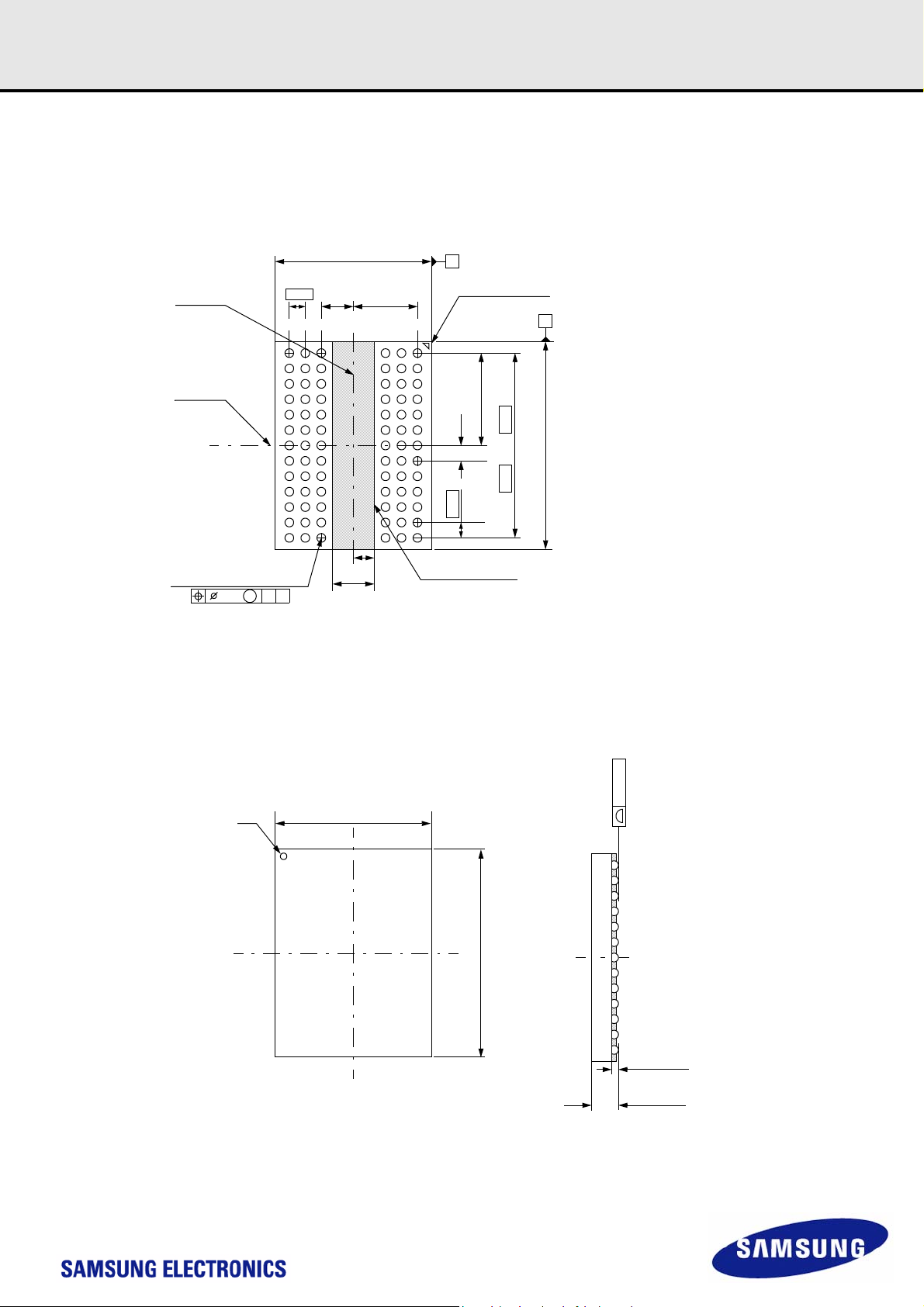
3. Package pinout/Mechanical Dimension & Addressing
3.1 x4 Package Pinout (Top view) : 78ball FBGA Package
1 2 3 4 5 6 7 8 9
Rev. 1.31
A
B
C
D
E
V
V
V
V
V
REFDQ
SS
SS
DDQ
SSQ
F NC
G ODT
V
V
DD
SSQ
NC NC
DQ0 DM
V
V
SSQ
DQ2 DQS DQ1 DQ3
NC DQS
V
DDQ
V
SS
V
DD
RAS CK
CAS CK
V
DD
NC NC NC
V
V
V
SS
SS
SS
DD
H NC CS WE A10/AP ZQ NC H
J
K
L
M
N
V
SS
V
DD
V
SS
V
DD
V
SS
BA0 BA2 NC
A3 A0 A12/BC BA1
A5 A2 A1 A4
A7 A9 A11 A6
RESET A13 A14 A8
Ball Locations (x4)
Populated ball
Ball not populated
Top view
(See the balls through the package)
V
REFCA
1234 89567
A
B
C
D
E
F
G
H
J
K
L
M
N
V
DD
V
DDQ
V
SSQ
V
SSQ
V
DDQ
NC F
CKE G
V
SS
V
DD
V
SS
V
DD
V
SS
A
B
C
D
E
J
K
L
M
N
- 6 -
K4B2G0446C
http://www.BDTIC.com/SAMSUNG
K4B2G0846C
datasheet DDR3 SDRAM
3.2 x8 Package Pinout (Top view) : 78ball FBGA Package
1 2 3 4 5 6 7 8 9
Rev. 1.31
A
B
C
D
E
V
V
V
V
V
REFDQ
SS
SS
DDQ
SSQ
F NC
G ODT
V
V
DD
SSQ
NC NU/TDQS
DQ0 DM/TDQS
V
V
SSQ
DQ2 DQS DQ1 DQ3
DQ6 DQS
V
V
V
DDQ
SS
DD
DQ4 DQ7 DQ5
RAS CK
CAS CK
V
DD
V
V
V
SS
SS
SS
DD
H NC CS WE A10/AP ZQ NC H
J
K
L
M
N
V
SS
V
DD
V
SS
V
DD
V
SS
BA0 BA2 NC
A3 A0 A12/BC BA1
A5 A2 A1 A4
A7 A9 A11 A6
RESET A13 A14 A8
Ball Locations (x8)
Populated ball
Ball not populated
Top view
(See the balls through the package)
V
REFCA
1234 89567
A
B
C
D
E
F
G
H
J
K
L
M
N
V
DD
V
DDQ
V
SSQ
V
SSQ
V
DDQ
NC F
CKE G
V
SS
V
DD
V
SS
V
DD
V
SS
A
B
C
D
E
J
K
L
M
N
- 7 -
K4B2G0446C
http://www.BDTIC.com/SAMSUNG
K4B2G0846C
3.3 FBGA Package Dimension (x4/x8)
Rev. 1.31
datasheet DDR3 SDRAM
(Datum A)
(Datum B)
78 - ∅0.45 Solder ball
(Post Reflow ∅0.50 ± 0.05)
0.2 ABM
0.80
A
B
C
D
E
F
G
H
J
K
L
M
N
7.50 ± 0.10
1.60
876543219
3.20
(0.95)
(1.90)
BOTTOM VIEW
A
#A1 INDEX MARK
4.80
0.80
0.80
MOLDING AREA
Units : Millimeters
B
11.00 ± 0.10
0.80 x 12 = 9.60
#A1
7.50 ± 0.10
TOP VIEW
0.10MAX
11.00 ± 0.10
0.35 ± 0.05
1.10 ± 0.10
- 8 -
K4B2G0446C
http://www.BDTIC.com/SAMSUNG
K4B2G0846C
datasheet DDR3 SDRAM
4. Input/Output Functional Description
[ Table 3 ] Input/Output function description
Symbol Typ e Function
CK, CK
CKE Input
CS
ODT Input
, CAS, WE Input Command Inputs: RAS, CAS and WE (along with CS) define the command being entered.
RAS
DM
(DMU), (DML)
BA0 - BA2 Input
A0 - A14 Input
A10 / AP Input
A12 / BC
RESET
DQ Input/Output Data Input/ Output: Bi-directional data bus.
DQS, (DQS
TDQS, (TDQS
V
V
) Input/Output
NC No Connect: No internal electrical connection is present.
V
DDQ
V
SSQ
V
DD
V
SS
REFDQ
REFCA
ZQ Supply Reference Pin for ZQ calibration
Input
Input
Input
Input
Input
)Output
Supply DQ Power Supply: 1.5V +/- 0.075V
Supply DQ Ground
Supply Power Supply: 1.5V +/- 0.075V
Supply Ground
Supply Reference voltage for DQ
Supply Reference voltage for CA
NOTE : Input only pins (BA0-BA2, A0-A14, RAS, CAS, WE, CS, CKE, ODT and RESET) do not supply termination.
Clock: CK and CK
the positive edge of CK and negative edge of CK
Clock Enable: CKE HIGH activates, and CKE Low deactivates, internal clock signals and device input buffers and
output drivers. Taking CKE Low provides Precharge Power-Down and Self Refresh operation (all banks idle), or
Active Power-Down (Row Active in any bank). CKE is asynchronous for self refresh exit. After V
stable during the power on and initialization sequence, it must be maintained during all operations (including SelfRefresh). CKE must be maintained high throughout read and write accesses. Input buffers, excluding CK, CK
and CKE are disabled during power-down. Input buffers, excluding CKE, are disabled during Self -Refresh.
Chip Select: All commands are masked when CS
systems with multiple Ranks. CS
On Die Termination: ODT (registered HIGH) enables termination resistance internal to the DDR3 SDRAM. When
enabled, ODT is only applied to each DQ, DQS, DQS
Register A11=1 in MR1) signal for x8 configurations. The ODT pin will be ignored if the Mode Register (MR1) is programmed to disable ODT.
Input Data Mask: DM is an input mask signal for write data. Input data is masked when DM is sampled HIGH coincident with that input data during a Write access. DM is sampled on both edges of DQS. For x8 device, the function of
DM or TDQS/TDQS
Bank Address Inputs: BA0 - BA2 define to which bank an Active, Read, Write or Precharge command is being
applied. Bank address also determines if the mode register or extended mode register is to be accessed during a
MRS cycle.
Address Inputs: Provided the row address for Active commands and the column address for Read/Write commands
to select one location out of the memory array in the respective bank. (A10/AP and A12/BC
see below)
The address inputs also provide the op-code during Mode Register Set commands.
Autoprecharge: A10 is sampled during Read/Write commands to determine whether Autoprecharge should be performed to the accessed bank after the Read/Write operation. (HIGH:Autoprecharge; LOW: No Autoprecharge)
A10 is sampled during a Precharge command to determine whether the Precharge applies to one bank (A10 LOW) or
all banks (A10 HIGH). if only one bank is to be precharged, the bank is selected by bank addresses.
Burst Chop:A12 is sampled during Read and Write commands to determine if burst chop(on-the-fly) will be performed. (HIGH : no burst chop, LOW : burst chopped). See command truth table for details
Active Low Asynchronous Reset: Reset is active when RESET
must be HIGH during normal operation. RESET is a CMOS rail to rail signal with DC high and low at 80% and
RESET
20% of V
Data Strobe: Output with read data, input with write data. Edge-aligned with read data, centered in write data. For the
x16, DQSL: corresponds to the data on DQL0-DQL7; DQSU corresponds to the data on DQU0-DQU7. The data
strobe DQS, DQSL and DQSU are paired with differential signals DQS, DQSL and DQSU, respectively, to provide differential pair signaling to the system during reads and writes. DDR3 SDRAM supports differential data strobe only and
does not support single-ended.
Termination Data Strobe: TDQS/TDQS
MR1, DRAM will enable the same termination resistance function on TDQS/TDQS
disabled via mode register A11=0 in MR1, DM/TDQS will provide the data mask function and TDQS
x16 DRAMs must disable the TDQS function via mode register A11=0 in MR1.
DD
are differential clock inputs. All address and control input signals are sampled on the crossing of
. Output (read) data is referenced to the crossings of CK and CK
is registered HIGH. CS provides for external Rank selection on
is considered part of the command code.
and DM/TDQS, NU/TDQS (When TDQS is enabled via Mode
is enabled by Mode Register A11 setting in MR1.
is LOW, and inactive when RESET is HIGH.
, i.e. 1.20V for DC high and 0.30V for DC low.
is applicable for X8 DRAMs only. When enabled via Mode Register A11=1 in
Rev. 1.31
has become
REFCA
, ODT
have additional functions,
that is applied to DQS/DQS. When
is not used. x4/
- 9 -
K4B2G0446C
http://www.BDTIC.com/SAMSUNG
K4B2G0846C
5. DDR3 SDRAM Addressing
1Gb
Configuration 256Mb x 4 128Mb x 8 64Mb x 16
# of Bank 8 8 8
Bank Address BA0 - BA2 BA0 - BA2 BA0 - BA2
Auto precharge A
Row Address A
Column Address A0 - A9,A11 A0 - A9 A0 - A9
BC switch on the fly A12/BC A12/BC A12/BC
Page size
2Gb
Configuration 512Mb x 4 256Mb x 8 128Mb x 16
# of Bank 8 8 8
Bank Address BA0 - BA2 BA0 - BA2 BA0 - BA2
Auto precharge A
Row Address A
Column Address A0 - A9,A11 A0 - A9 A0 - A9
BC switch on the fly A12/BC A12/BC A12/BC
Page size
*1
*1
Rev. 1.31
datasheet DDR3 SDRAM
10/AP A10/AP A10/AP
0 - A13 A0 - A13 A0 - A12
1 KB 1 KB 2 KB
10/AP A10/AP A10/AP
0 - A14 A0 - A14 A0 - A13
1 KB 1 KB 2 KB
4Gb
Configuration 1Gb x 4 512Mb x 8 256Mb x 16
# of Bank 8 8 8
Bank Address BA0 - BA2 BA0 - BA2 BA0 - BA2
Auto precharge A
Row Address A
Column Address A0 - A9,A11 A0 - A9 A0 - A9
BC switch on the fly A12/BC A12/BC A12/BC
Page size
*1
10/AP A10/AP A10/AP
0 - A15 A0 - A15 A0 - A14
1 KB 1 KB 2 KB
8Gb
Configuration 2Gb x 4 1Gb x 8 512Mb x 16
# of Bank 8 8 8
Bank Address BA0 - BA2 BA0 - BA2 BA0 - BA2
Auto precharge A
Row Address A
Column Address A0 - A9,A11 ,A13 A0 - A9,A11 A0 - A9
BC switch on the fly A12/BC A12/BC A12/BC
Page size
NOTE 1 : Page size is the number of bytes of data delivered from the array to the internal sense amplifiers when an ACTIVE command is registered.
Page size is per bank, calcula
where, COLBITS = the number of column address bits, ORG = the number of I/O (DQ) bits
*1
ted as follows: page size = 2
10/AP A10/AP A10/AP
0 - A15 A0 - A15 A0 - A15
2 KB 2 KB 2 KB
COLBITS
* ORG÷8
- 10 -
Rev. 1.31
http://www.BDTIC.com/SAMSUNG
K4B2G0446C
K4B2G0846C
datasheet DDR3 SDRAM
6. Absolute Maximum Ratings
6.1 Absolute Maximum DC Ratings
[ Table 4 ] Absolute Maximum DC Ratings
Symbol Parameter Rating Units NOTE
V
DD
Voltage on V
V
DDQ
V
NOTE :
1. Stresses greater than those listed under “Absolute Maximum Ratings” may
device at these or any other conditions above those indicated in the operational sections of this specification is not implied. Exposure to absolute maximum rating conditions
for extended periods may affect reliability.
2. Storage Temperature is the case surface temperature on the cente
3. V
DD
equal to or less than 300mV.
Voltage on any pin relative to Vss -0.4 V ~ 1.975 V V 1
IN, VOUT
Storage Temperature -55 to +100 °C 1, 2
T
STG
and V
DDQ
Voltage on VDD pin relative to Vss -0.4 V ~ 1.975 V V 1,3
pin relative to Vss -0.4 V ~ 1.975 V V 1,3
DDQ
cause permanent damage to the device. This is a stress rating only and functional operation of the
must be within 300mV of each other at all times; and V
r/top side of the DRAM. For the measurement conditions, please refer to JESD51-2 standard.
must be not greater than 0.6 x V
REF
, When VDD and V
DDQ
are less than 500mV; V
DDQ
REF
may be
6.2 DRAM Component Operating Temperature Range
[ Table 5 ] Temperature Range
Symbol Parameter rating Unit NOTE
T
OPER
NOTE :
1. Operating Temperature T
JESD51-2.
2. The Normal Temperature Range specifies the temperatures where a
tained between 0-85°C u
3. Some applications require operation of the Extended Temperature Range between 85°C an
following additional conditions apply:
a) Refresh commands must be doubled in frequency, therefo
b) If Self-Refresh operation is required in the Extended Temperature
Range capability (MR2 A6 = 0
is the case surface temperature on the center/top side of the DRAM. For measurement conditions, please refer to the JEDEC document
OPER
nder all operating conditions
Operating Temperature Range 0 to 95 °C 1, 2, 3
ll DRAM specifications will be supported. During operation, the DRAM case temperature must be main-
d 95°C case temperature. Full specifications are guaranteed in this range, but the
re reducing the refresh interval tREFI to 3.9us.
and MR2 A7 = 1b), in this case IDD6 current can be increased around 10~20% than normal Temperature range.
b
Range, then it is mandatory to either use the Manual Self-Refresh mode with Extended Temperature
7. AC & DC Operating Conditions
7.1 Recommended DC operating Conditions (SSTL_1.5)
[ Table 6 ] Recommended DC Operating Conditions
Symbol Parameter
V
DD
V
DDQ
NOTE :
1. Under all conditions V
2. V
tracks with VDD. AC parameters are measured with VDD and V
DDQ
Supply Voltage 1.425 1.5 1.575 V 1,2
Supply Voltage for Output 1.425 1.5 1.575 V 1,2
must be less than or equal to VDD.
DDQ
tied together.
DDQ
Min. Typ . Max.
Rating
Units NOTE
- 11 -
K4B2G0446C
http://www.BDTIC.com/SAMSUNG
K4B2G0846C
datasheet DDR3 SDRAM
8. AC & DC Input Measurement Levels
8.1 AC & DC Logic input levels for single-ended signals
[ Table 7 ] Single-ended AC & DC input levels for Command and Address
Symbol Parameter
V
(DC100)
IH.CA
(DC100)
V
IL.CA
V
(AC175)
IH.CA
(AC175)
V
IL.CA
(AC150)
V
IH.CA
(AC150)
V
IL.CA
V
REFCA
NOTE :
1. For input only pins except RESET
2. See ’Overshoot/Undershoot Specification’ on page 19.
3. The AC peak noise on V
4. For reference : approx. V
(dc) is used as a simplified symbol for V
5. V
IH
(dc) is used as a simplified symbol for V
6. V
IL
7. V
(ac) is used as a simplified symbol for V
IH
used when VREF + 150mV is referenced.
(ac) is used as a simplified symbol for V
8. V
IL
when V
REF
DC input logic high
DC input logic low
AC input logic high
AC input logic low -
AC input logic high
AC input logic low -
Reference Voltage for ADD,
(DC)
CMD inputs
, V
may not allow V
REF
/2 ± 15mV
DD
- 150mV is referenced.
REF
= V
(DC)
REFCA
to deviate from V
REF
(DC100)
IH.CA
(DC100)
IL.CA
(AC175) and V
IH.CA
(AC175) and V
IL.CA
Min. Max.
V
REF
V
V
REF
V
REF
0.49*V
(DC) by more than ± 1% VDD (for reference : approx. ± 15mV)
REF
(AC150); V
IH.CA
(AC150); V
IL.CA
DDR3-800/1066/1333/1600
+ 100 V
SS
+ 175
+150
DD
(AC175) value is used when V
IH.CA
(AC175) value is used when V
IL.CA
DD
V
- 100
REF
- mV 1,2,7
V
- 175
REF
- mV 1,2,7
V
-150
REF
0.51*V
DD
+ 175mV is referenced and V
REF
- 175mV is referenced and V
REF
Rev. 1.31
Unit NOTE
mV 1,5
mV 1,6
mV 1,2,8
mV 1,2,8
V3,4
(AC150) value is
IH.CA
(AC150) value is used
IL.CA
[ Table 8 ] Single-ended AC & DC input levels for DQ and DM
Symbol Parameter
V
(DC100)
IH.DQ
(DC100)
V
IL.DQ
V
(AC175)
IH.DQ
(AC175)
V
IL.DQ
(AC150)
V
IH.DQ
(AC150)
V
IL.DQ
V
REF
DQ
NOTE :
1. For input only pins except RESET
2. See ’Overshoot/Undershoot Specification’ on page 19.
3. The AC peak noise on V
4. For reference : approx. V
5. V
(dc) is used as a simplified symbol for V
IH
(dc) is used as a simplified symbol for V
6. V
IL
7. V
(ac) is used as a simplified symbol for V
IH
when V
(ac) is used as a simplified symbol for V
8. V
IL
- 150mV is referenced.
V
REF
DC input logic high
DC input logic low
AC input logic high
AC input logic low -
AC input logic high
AC input logic low NOTE 2
Reference Voltage for DQ,
(DC)
DM inputs
, V
= V
REF
REFDQ
may not allow V
REF
DD
+ 150mV is referenced.
REF
/2 ± 15mV
REF
IH.DQ
IL.DQ
IH.DQ
IL.DQ
(DC)
to deviate from V
(DC100)
(DC100)
(AC175), V
(AC175), V
DDR3-800/1066 DDR3-1333/1600
Min. Max. Min. Max.
V
+ 100 V
REF
V
SS
V
+ 175
REF
V
+ 150
REF
0.49*V
DD
REF
(AC150) ; V
IH.DQ
(AC150) ; V
IL.DQ
V
DD
V
- 100 V
REF
+ 100 V
REF
SS
- - - mV 1,2,7
V
- 175
REF
NOTE 2
V
- 150
REF
0.51*V
DD
(DC) by more than ± 1% VDD (for reference : approx. ± 15mV)
(AC175) value is used when V
IH.DQ
(AC175) value is used when V
IL.DQ
- - mV 1,2,8
V
+ 150
REF
NOTE 2
0.49*V
DD
+ 175mV is referenced, V
REF
- 175mV is referenced, V
REF
Unit NOTE
DD
V
- 100
REF
mV 1,5
mV 1,6
NOTE 2 mV 1,2,7
V
- 150
REF
0.51*V
DD
IL.DQ
mV 1,2,8
V3,4
(AC150) value is used
IH.DQ
(AC150) value is used when
- 12 -
K4B2G0446C
http://www.BDTIC.com/SAMSUNG
K4B2G0846C
Rev. 1.31
datasheet DDR3 SDRAM
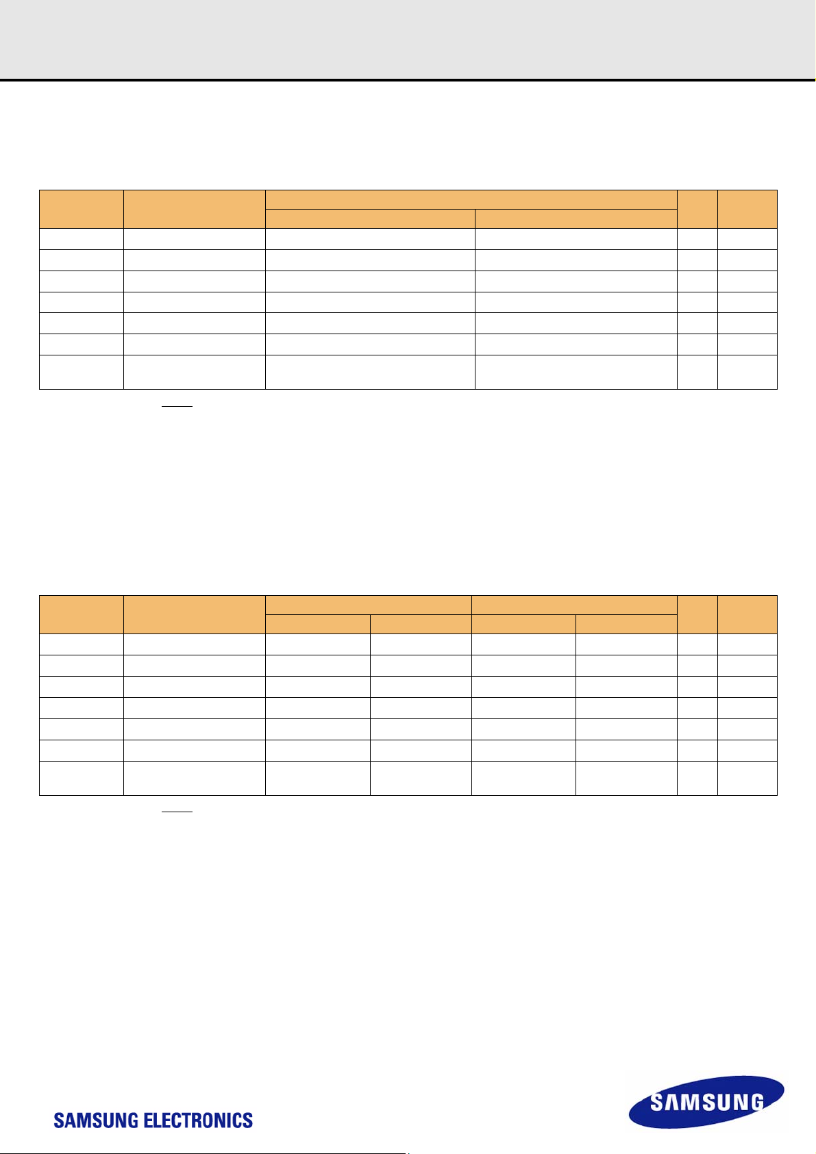
8.2 V
The dc-tolerance limits and ac-noise limits for the reference voltages V
V
REF
V
REF
page 12. Furthermore V
Tolerances
REF
(t) as a function of time. (V
(DC) is the linear average of V
REF
(t) may temporarily deviate from V
REF
voltage
stands for V
(t) over a very long period of time (e.g. 1 sec). This average has to meet the min/max requirement in Table 7 on
REF
REFCA
and V
likewise).
REFDQ
(DC) by no more than ± 1% VDD.
REF
REFCA
and V
are illustrate in Figure 1. It shows a valid reference voltage
REFDQ
V
DD
V
SS
time
Figure 1. Illustration of V
The voltage levels for setup and hold time measurements VIH(AC), VIH(DC), VIL(AC) and VIL(DC) are dependent on V
" shall be understood as V
"V
REF
This clarifies, that dc-variations of V
which setup and hold is measured. System timing and voltage budgets need to account for V
data-eye of the input signals.
This also clarifies that the DRAM setup/hold specification and derating values need to include time and voltage associated with V
and voltage effects due to ac-noise on V
(DC), as defined in Figure 1.
REF
affect the absolute voltage a signal has to reach to achieve a valid high or low level and therefore the time to
REF
up to the specified limit (+/-1% of VDD) are included in DRAM timings and their associated deratings.
REF
(DC) tolerance and VREF ac-noise limits
REF
(DC) deviations from the optimum position within the
REF
REF
.
ac-noise. Timing
REF
- 13 -
K4B2G0446C
http://www.BDTIC.com/SAMSUNG
K4B2G0846C
datasheet DDR3 SDRAM
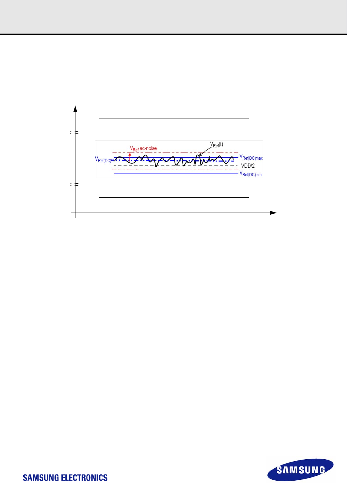
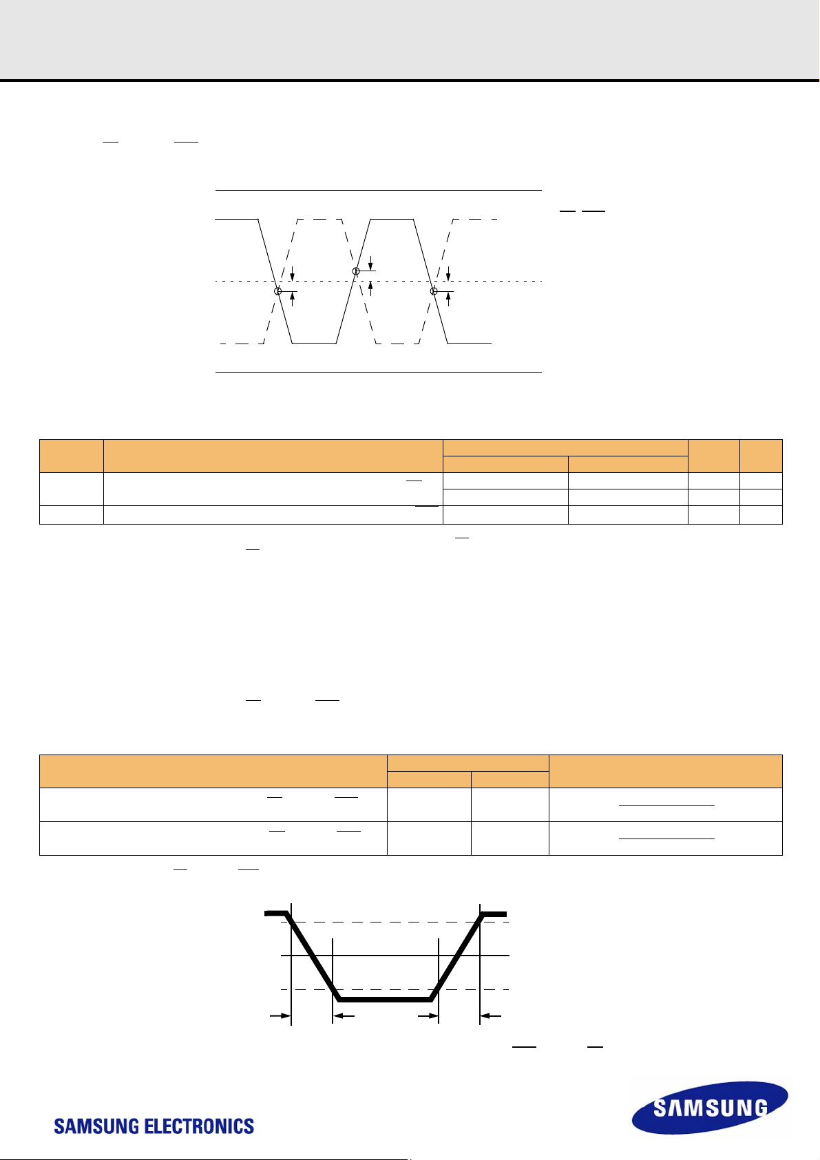
8.3 AC & DC Logic Input Levels for Differential Signals
8.3.1 Differential signals definition
tDVAC
VIH.DIFF.AC.MIN
.DIFF.MIN
V
IH
0.0
half cycle
V
.DIFF.MAX
IL
.DIFF.AC.MAX
V
IL
Rev. 1.31
Differential Input Voltage (i.e. DQS-DQS, CK-CK)
Figure 2. Definition of differential ac-swing and "time above ac level" tDVAC
tDVAC
time
8.3.2 Differential swing requirement for clock (CK - CK) and strobe (DQS - DQS)
[ Table 9 ] Differential AC & DC Input Levels
Symbol Parameter
V
IHdiff
V
ILdiff
(AC)
V
IHdiff
V
(AC)
ILdiff
NOTE :
1. Used to define a differential signal slew-rate.
2. for CK - CK
level is used for a signal group, then the reduced level applies also here.
3. These values are not defined, however they single-ended signals CK, CK
V
IL
[ Table 10 ] Allowed time before ringback (tDVAC) for CK - CK and DQS - DQS
use VIH/VIL(AC) of ADD/CMD and V
(DC)min) for single-ended signals as well as the limitations for overshoot and undershoot. Refer to "overshoot and Undershoot Specification"
Slew Rate [V/ns]
differential input high +0.2 NOTE 3 V 1
differential input low NOTE 3 -0.2 V 1
differential input high ac
differential input low ac NOTE 3
; for DQS - DQS, DQSL - DQSL, DQSU - DQSU use VIH/VIL(AC) of DQs and V
REFCA
> 4.0 75 - 175 -
4.0 57 - 170 -
3.0 50 - 167 -
2.0 38 - 163 -
1.8 34 - 162 -
1.6 29 - 161 -
1.4 22 - 159 -
1.2 13 - 155 -
1.0 0 - 150 -
< 1.0 0 - 150 -
2 x (VIH(AC) - V
tDVAC [ps] @ |V
min max min max
DDR3-800/1066/1333/1600
min max
)
REF
, DQS, DQS, DQSL, DQSL, DQSU, DQSU need to be within the respective limits (VIH(DC) max,
(AC)| = 350mV tDVAC [ps] @ |V
IH/Ldiff
NOTE 3 V 2
2 x (VIL(AC) - V
REF
)
unit NOTE
V2
; if a reduced ac-high or ac-low
REFDQ
(AC)| = 300mV
IH/Ldiff
- 14 -
Rev. 1.31
http://www.BDTIC.com/SAMSUNG
K4B2G0446C
K4B2G0846C
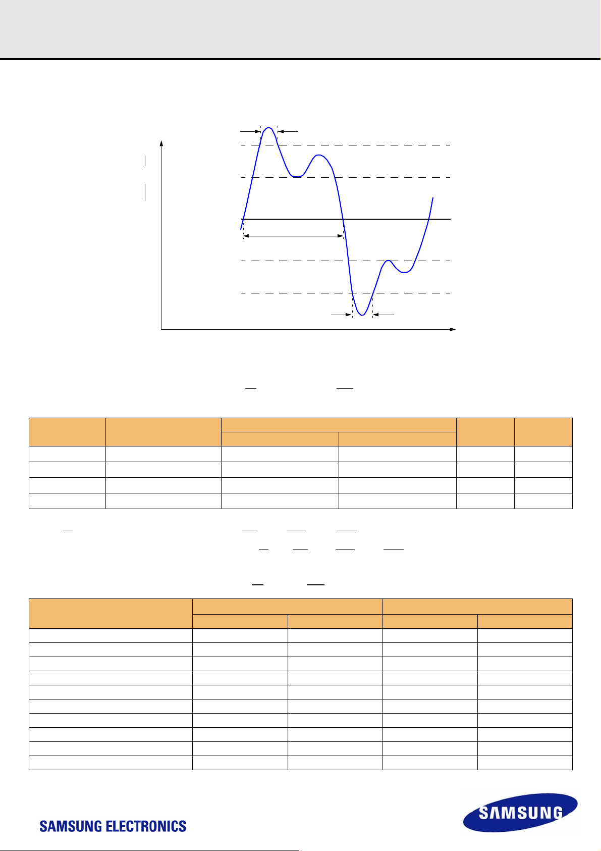
8.3.3 Single-ended requirements for differential signals
Each individual component of a differential signal (CK, DQS, DQSL, DQSU, CK, DQS, DQSL, or DQSU) has also to comply with certain requirements for
single-ended signals.
CK and CK
half-cycle.
DQS, DQSL, DQSU, DQS
proceeding and following a valid transition.
Note that the applicable ac-levels for ADD/CMD and DQ’s might be different per speed-bin etc. E.g. if V
nals, then these ac-levels apply also for the single-ended signals CK and CK
have to approximately reach V
, DQSL have to reach V
SEH
min / V
SEH
datasheet DDR3 SDRAM
max [approximately equal to the ac-levels { VIH(AC) / VIL(AC)} for ADD/CMD signals] in every
SEL
min / V
max [approximately the ac-levels { VIH(AC) / VIL(AC)} for DQ signals] in every half-cycle
SEL
150(AC)/VIL150(AC) is used for ADD/CMD sig-
IH
.
VDD or V
/2 or V
V
DD
VSS or V
Note that while ADD/CMD and DQ signal requirements are with respect to V
with respect to V
ended components of differential signals the requirement to reach V
mode characteristics of these signals.
/2; this is nominally the same. The transition of single-ended signals through the ac-levels is used to measure setup time. For single-
DD
DDQ
V
min
SEH
V
SEH
/2
DDQ
V
max
SEL
SSQ
Figure 3. Single-ended requirement for differential signals
max, V
SEL
CK or DQS
V
SEL
time
, the single-ended components of differential signals have a requirement
REF
min has no bearing on timing, but adds a restriction on the common
SEH
[ Table 11 ] Single-ended levels for CK, DQS, DQSL, DQSU, CK
Symbol Parameter
V
SEH
V
SEL
NOTE :
1. For CK, CK
2. V
IH
reduced level applies also here
3. These values are not defined, however the single-ended signals CK, CK
limits (V
Specification"
use VIH/VIL(AC) of ADD/CMD; for strobes (DQS, DQS, DQSL, DQSL, DQSU, DQSU) use VIH/VIL(AC) of DQs.
(AC)/VIL(AC) for DQs is based on V
(DC) max, VIL(DC)min) for single-ended signals as well as the limitations for overshoot and undershoot. Refer to "Overshoot and Undershoot
IH
Single-ended high-level for strobes
Single-ended high-level for CK, CK
Single-ended low-level for strobes NOTE3
Single-ended low-level for CK, CK
; VIH(AC)/VIL(AC) for ADD/CMD is based on V
REFDQ
, DQS, DQSL, or DQSU
DDR3-800/1066/1333/1600
Min Max
/2)+0.175
(V
DD
(VDD/2)+0.175
NOTE3
; if a reduced ac-high or ac-low level is used for a signal group, then the
REFCA
, DQS, DQS, DQSL, DQSL, DQSU, DQSU need to be within the respective
- 15 -
NOTE3 V 1, 2
NOTE3 V 1, 2
/2)-0.175
(V
DD
/2)-0.175
(V
DD
Unit NOTE
V1, 2
V1, 2
Rev. 1.31
http://www.BDTIC.com/SAMSUNG
K4B2G0446C
K4B2G0846C
datasheet DDR3 SDRAM
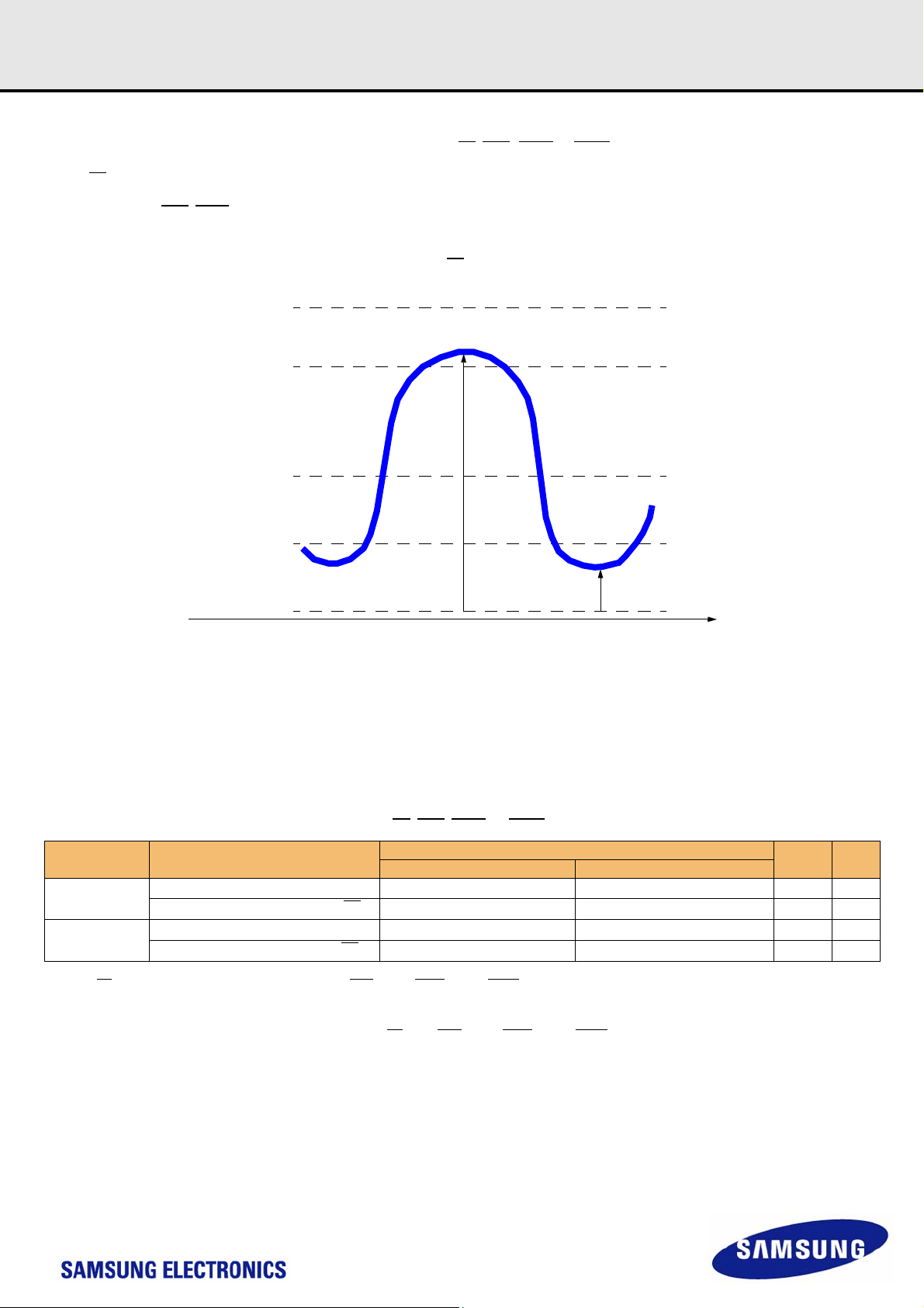
8.4 Differential Input Cross Point Voltage
To guarantee tight setup and hold times as well as output skew parameters with respect to clock and strobe, each cross point voltage of differential input
signals (CK, CK
cross point of true and complement signal to the mid level between of V
[ Table 12 ] Cross point voltage for differential input signals (CK, DQS)
Symbol Parameter
V
IX
V
IX
NOTE :
1. Extended range for V
±250 mV, and the differential slew rate of CK-CK
and DQS, DQS) must meet the requirements in below table. The differential input cross point voltage VIX is measured from the actual
and VSS.
DD
V
DD
CK, DQS
V
IX
VDD/2
V
IX
V
IX
CK, DQS
V
SS
Figure 4. VIX Definition
Differential Input Cross Point Voltage relative to VDD/2 for CK,CK
Differential Input Cross Point Voltage relative to VDD/2 for DQS,DQS
is only allowed for clock and if single-ended clock input signals CKand CK are monotonic, have a single-ended swing V
IX
is larger than 3 V/ ns. Refer to Table 11 on page 15 for V
DDR3-800/1066/1333/1600
Min Max
-150 150 mV
-175 175 mV 1
-150 150 mV
SEL
and V
standard values.
SEH
SEL
/ V
Unit NOTE
of at least VDD/2
SEH
8.5 Slew rate definition for Differential Input Signals
See 14.3 “Address/Command Setup, Hold and Derating :” on page 48 for single-ended slew rate definitions for address and command signals.
See 14.4 “Data Setup, Hold and Slew Rate Derating :” on page 54 for single-ended slew rate definitions for data signals.
8.6 Slew rate definitions for Differential Input Signals
Input slew rate for differential signals (CK, CK and DQS, DQS) are defined and measured as shown in Table 13 and Figure 5.
[ Table 13 ] Differential input slew rate definition
Description
Differential input slew rate for rising edge (CK-CK
Differential input slew rate for falling edge (CK-CK
NOTE :
The differential signal (i.e. CK - CK
and DQS - DQS) must be linear between these thresholds.
and DQS-DQS)
and DQS-DQS)
Measured
From To
V
ILdiffmax
V
IHdiffmin
V
IHdiffmin
V
ILdiffmax
V
IHdiffmin
0
V
ILdiffmax
Defined by
V
IHdiffmin
Delta TRdiff
V
IHdiffmin
Delta TFdiff
- V
- V
ILdiffmax
ILdiffmax
delta TFdiff
Figure 5. Differential Input Slew Rate definition for DQS, DQS, and CK, CK
delta TRdiff
- 16 -
K4B2G0446C
http://www.BDTIC.com/SAMSUNG
K4B2G0846C
datasheet DDR3 SDRAM
9. AC & DC Output Measurement Levels
9.1 Single-ended AC & DC Output Levels
[ Table 14 ] Single-ended AC & DC output levels
Symbol Parameter DDR3-800/1066/1333/1600 Units NOTE
(DC) DC output high measurement level (for IV curve linearity) 0.8 x V
V
OH
(DC) DC output mid measurement level (for IV curve linearity) 0.5 x V
V
OM
(DC) DC output low measurement level (for IV curve linearity) 0.2 x V
V
OL
(AC) AC output high measurement level (for output SR) VTT + 0.1 x V
V
OH
(AC) AC output low measurement level (for output SR) VTT - 0.1 x V
V
OL
NOTE : 1. The swing of +/-0.1 x V
load of 25Ω to V
TT=VDDQ
is based on approximately 50% of the static single ended output high or low swing with a driver impedance of 40Ω and an effective test
DDQ
/2.
DDQ
DDQ
DDQ
DDQ
DDQ
9.2 Differential AC & DC Output Levels
[ Table 15 ] Differential AC & DC output levels
Symbol Parameter DDR3-800/1066/1333/1600 Units NOTE
(AC) AC differential output high measurement level (for output SR) +0.2 x V
V
OHdiff
(AC) AC differential output low measurement level (for output SR) -0.2 x V
V
OLdiff
NOTE : 1. The swing of +/-0.2xV
load of 25Ω to V
TT=VDDQ
is based on approximately 50% of the static single ended output high or low swing with a driver impedance of 40Ω and an effective test
DDQ
/2 at each of the differential outputs.
DDQ
DDQ
V
V
V
V1
V1
V1
V1
Rev. 1.31
9.3 Single-ended Output Slew Rate
With the reference load for timing measurements, output slew rate for falling and rising edges is defined and measured between VOL(AC) and VOH(AC)
for single ended signals as shown in Table 16 and Figure 6.
[ Table 16 ] Single-ended output slew rate definition
Description
Single ended output slew rate for rising edge
Single ended output slew rate for falling edge
NOTE : Output slew rate is verified by design and characterization, and may not be subject to production test.
[ Table 17 ] Single-ended output slew rate
Parameter Symbol
Single ended output slew rate SRQse 2.5 5 2.5 5 2.5 5 2.5 5 V/ns
Description : SR : Slew Rate
Q : Query Output (like in DQ, which stands for Data-in, Query-Output)
se : Single-ended Signals
For Ron = RZQ/7 setting
DDR3-800 DDR3-1066 DDR3-1333 DDR3-1600
Min Max Min Max Min Max Min Max
Measured
From To
V
(AC) VOH(AC)
OL
V
(AC) VOL(AC)
OH
V
OH(AC)
Defined by
(AC)-VOL(AC)
V
OH
Delta TRse
(AC)-VOL(AC)
V
OH
Delta TFse
Units
Figure 6. Single-ended Output Slew Rate Definition
- 17 -
VTT
V
OL(AC)
delta TRsedelta TFse
Rev. 1.31
http://www.BDTIC.com/SAMSUNG
K4B2G0446C
K4B2G0846C
datasheet DDR3 SDRAM
9.4 Differential Output Slew Rate
With the reference load for timing measurements, output slew rate for falling and rising edges is defined and measured between V
(AC) for differential signals as shown in Table 18 and Figure 7.
diff
[ Table 18 ] Differential output slew rate definition
Description
Differential output slew rate for rising edge
Differential output slew rate for falling edge
NOTE : Output slew rate is verified by design and characterization, and may not be subject to production test.
[ Table 19 ] Differential output slew rate
Parameter Symbol
Differential output slew rate SRQdiff 5 10 5 10 5 10 5 10 V/ns
Description : SR : Slew Rate
Q : Query Output (like in DQ, which stands for Data-in, Query-Output)
diff : Differential Signals
For Ron = RZQ/7 setting
V
V
DDR3-800 DDR3-1066 DDR3-1333 DDR3-1600
Min Max Min Max Min Max Min Max
Measured
From To
(AC) V
OLdiff
(AC) V
OHdiff
OHdiff
OLdiff
(AC)
(AC)
V
OHdiff
V
OHdiff
Defined by
(AC)-V
OLdiff
Delta TRdiff
(AC)-V
OLdiff
Delta TFdiff
(AC)
(AC)
OLdiff
(AC) and V
Units
OH-
V
(AC)
OHdiff
VTT
(AC)
V
OLdiff
delta TRdiffdelta TFdiff
Figure 7. Differential Output Slew Rate Definition
9.5 Reference Load for AC Timing and Output Slew Rate
Figure 8 represents the effective reference load of 25 ohms used in defining the relevant AC timing parameters of the device as well as output slew rate
measurements.
It is not intended as a precise representation of any particular system environment or a depiction of the actual load presented by a production tester. System designers should use IBIS or other simulation tools to correlate the timing reference load to a system environment. Manufacturers correlate to their
production test conditions, generally one or more coaxial transmission lines terminated at the tester electronics.
V
DDQ
CK/CK
DUT
Reference
Point
Figure 8. Reference Load for AC Timing and Output Slew Rate
DQ
DQS
DQS
- 18 -
25
Ω
VTT = V
DDQ
/2

Rev. 1.31
http://www.BDTIC.com/SAMSUNG
K4B2G0446C
K4B2G0846C
datasheet DDR3 SDRAM
9.6 Overshoot/Undershoot Specification
9.6.1 Address and Control Overshoot and Undershoot specifications
[ Table 20 ] AC overshoot/undershoot specification for Address and Control pins (A0-A12, BA0-BA2. CS. RAS. CAS. WE. CKE, ODT)
Parameter
Maximum peak amplitude allowed for overshoot area (See Figure 9) 0.4V 0.4V 0.4V 0.4V V
Maximum peak amplitude allowed for undershoot area (See Figure 9) 0.4V 0.4V 0.4V 0.4V V
Maximum overshoot area above V
Maximum undershoot area below V
Volts
(See Figure 9)
DD
(See Figure 9)
SS
V
DD
Maximum Amplitude
DDR3-800 DDR3-1066 DDR3-1333 DDR3-1600
0.67V-ns 0.5V-ns 0.4V-ns 0.33V-ns V-ns
0.67V-ns 0.5V-ns 0.4V-ns 0.33V-ns V-ns
(V)
V
SS
Specification
Overshoot Area
Unit
Maximum Amplitude
Time (ns)
Figure 9. Address and Control Overshoot and Undershoot Definition
9.6.2 Clock, Data, Strobe and Mask Overshoot and Undershoot Specifications
Undershoot Area
[ Table 21 ] AC overshoot/undershoot specification for Clock, Data, Strobe and Mask (DQ, DQS, DQS, DM, CK, CK)
Parameter
Maximum peak amplitude allowed for overshoot area (See Figure 10) 0.4V 0.4V 0.4V 0.4V V
Maximum peak amplitude allowed for undershoot area (See Figure 10) 0.4V 0.4V 0.4V 0.4V V
Maximum overshoot area above V
Maximum undershoot area below V
(See Figure 10)
DDQ
(See Figure 10)
SSQ
Maximum Amplitude
DDR3-800 DDR3-1066 DDR3-1333 DDR3-1600
0.25V-ns 0.19V-ns 0.15V-ns 0.13V-ns V-ns
0.25V-ns 0.19V-ns 0.15V-ns 0.13V-ns V-ns
Specification
Overshoot Area
V
Volts
DDQ
(V)
V
SSQ
Unit
Figure 10. Clock, Data, Strobe and Mask Overshoot and Undershoot Definition
Maximum Amplitude
Undershoot Area
Time (ns)
- 19 -

Rev. 1.31
http://www.BDTIC.com/SAMSUNG
K4B2G0446C
K4B2G0846C
datasheet DDR3 SDRAM
9.7 34ohm Output Driver DC Electrical Characteristics
A functional representation of the output buffer is shown below. Output driver impedance RON is defined by the value of external reference resistor RZQ
as follows:
= RZQ/7 (Nominal 34.3ohms +/- 10% with nominal RZQ=240ohm)
RON
34
The individual Pull-up and Pull-down resistors (RONpu and RONpd) are defined as follows
V
RONpu =
RONpd =
DDQ-VOUT
l Iout l
V
OUT
l Iout l
under the condition that RONpd is turned off
under the condition that RONpu is turned off
Output Driver
Ipu
V
DDQ
To
other
circuity
RON
RON
Ipd
Pu
Pd
Iout
DQ
V
Vout
SSQ
Figure 11. Output Driver : Definition of Voltages and Currents
[ Table 22 ] Output Driver DC Electrical Characteristics, assuming RZQ=240ohms ;
entire operating temperature range ; after proper ZQ calibration
RONnom Resistor Vout Min Nom Max Units NOTE
= 0.2 x V
V
OLdc
V
RON34pd
34Ohms
RON34pu
RON40pd
40Ohms
RON40pu
Mismatch between Pull-up and Pull-down,
MMpupd
NOTE :
1. The tolerance limits are specified after calibration with stable voltage and temperature. For the behavior of the tolerance limits if temperature or voltage changes after calibration, see following section on voltage and temperature sensitivity
2. The tolerance limits are specified under the condition that V
3. Pull-down and pull-up output driver impedance are recommended to be calibrated at 0.5 X V
above, e.g. calibration at 0.2 X V
4. Measurement definition for mismatch between pull-up and pull-down, MMpupd: Measure RONpu and RONpd. both at 0.5 X V
and 0.8 X V
DDQ
DDQ
= 0.5 x V
OMdc
V
= 0.8 x V
OHdc
= 0.2 x V
V
OLdc
= 0.5 x V
V
OMdc
= 0.8 x V
V
OHdc
V
= 0.2 x V
OLdc
V
= 0.5 x V
OMdc
= 0.8 x V
V
OHdc
= 0.2 x V
V
OLdc
V
= 0.5 x V
OMdc
V
= 0.8 x V
OHdc
= 0.5 x V
V
OMdc
= VDD and that V
DDQ
DDQ
DDQ
DDQ
DDQ
DDQ
DDQ
DDQ
DDQ
DDQ
DDQ
DDQ
DDQ
DDQ
0.6 1.0 1.1
0.9 1.0 1.1 1,2,3
0.9 1.0 1.4 1,2,3
0.9 1.0 1.4 1,2,3
RZQ/7
0.9 1.0 1.1 1,2,3
0.6 1.0 1.1 1,2,3
0.6 1.0 1.1
0.9 1.0 1.1 1,2,3
0.9 1.0 1.4 1,2,3
0.9 1.0 1.4 1,2,3
RZQ/6
0.9 1.0 1.1 1,2,3
0.6 1.0 1.1 1,2,3
-10 10 % 1,2,4
= V
SSQ
SS
. Other calibration schemes may be used to achieve the linearity spec shown
DDQ
:
DDQ
1,2,3
1,2,3
MMpupd =
RONpu - RONpd
RONnom
x 100
- 20 -

K4B2G0446C
http://www.BDTIC.com/SAMSUNG
K4B2G0846C
9.7.1 Output Drive Temperature and Voltage Sensitivity
If temperature and/or voltage change after calibration, the tolerance limits widen according to Table 23 and Table 24.
- V
∆T = T - T(@calibration); ∆V = V
*dRONdT and dRONdV are not subject to production test but are verified by design and characterization
[ Table 23 ] Output Driver Sensitivity Definition
RONPU@V
RON@V
RONPD@
[ Table 24 ] Output Driver Voltage and Temperature Sensitivity
Speed Bin 800/1066/1333 1600
OMDC
VOLDC
dTM
dR
ON
dRONdVM
dTL
dR
ON
dRONdVL
dR
dTH
ON
dRONdVH
OHDC
DDQ
(@calibration); VDD = V
DDQ
0.6 - dRONdTH * |∆T| - dR
0.9 - dRONdTM * |∆T| - dR
0.6 - dRONdTL * |∆T| - dR
Min Max Min Max
01.501.5
0 0.15 0 0.13 %/mV
01.501.5
0 0.15 0 0.13 %/mV
01.501.5
0 0.15 0 0.13 %/mV
datasheet DDR3 SDRAM
DDQ
Min Max Units
dVH * |∆V| 1.1 + dR
ON
dVM * |∆V| 1.1 + dR
ON
dVL * |∆V| 1.1 + dR
ON
dTH * |∆T| + dR
ON
dTM * |∆T| + dR
ON
dTL * |∆T| + dR
ON
dVH * |∆V|
ON
dVM * |∆V|
ON
dVL * |∆V|
ON
Rev. 1.31
RZQ/7
RZQ/7
RZQ/7
Units
%/°C
%/°C
%/°C
9.8 On-Die Termination (ODT) Levels and I-V Characteristics
On-Die Termination effective resistance RTT is defined by bits A9, A6 and A2 of MR1 register.
ODT is applied to the DQ,DM, DQS/DQS
A functional representation of the on-die termination is shown below. The individual pull-up and pull-down resistors (RTTpu and RTTpd) are defined as
follows :
V
RTTpu =
RTTpd =
DDQ-VOUT
l Iout l
V
OUT
l Iout l
and TDQS,TDQS (x8 devices only) pins.
under the condition that RTTpd is turned off
under the condition that RTTpu is turned off
Chip in Termination Mode
ODT
Ipu
To
other
circuitry
like
RCV,
...
RTT
RTT
Pu
Pd
Ipd
V
DDQ
Iout=Ipd-Ipu
DQ
Iout
V
OUT
Figure 12. On-Die Termination : Definition of Voltages and Currents
- 21 -
V
SSQ

K4B2G0446C
http://www.BDTIC.com/SAMSUNG
K4B2G0846C
9.8.1 ODT DC Electrical Characteristics
Rev. 1.31
datasheet DDR3 SDRAM
Table 25 provides and overview of the ODT DC electrical characteristics. They values for RTT
RTT
40pu80,
RTT
30pd60,
RTT
30pu60,
RTT
20pd40,
RTT
are not specification requirements, but can be used as design guide lines:
20pu40
60pd120,
RTT
60pu120,
RTT
120pd240,
RTT
120pu240,
RTT
40pd80,
[ Table 25 ] ODT DC Electrical Characteristics, assuming RZQ=240ohm +/- 1% entire operating temperature range; after proper ZQ calibration
MR1 (A9,A6,A2) RTT RESISTOR Vou t Min Nom Max Unit NOTE
(0,1,0) 120 ohm
(0,0,1) 60 ohm
(0,1,1) 40 ohm
(1,0,1) 30 ohm
(1,0,0) 20 ohm
Deviation of VM w.r.t V
DDQ
/2, ∆VM
RTT
RTT
RTT
RTT
RTT
RTT
RTT
RTT
RTT
RTT
RTT60
RTT
RTT
RTT
RTT
120pd240
120pu240
120
60pd240
60pu240
60
40pd240
40pu240
40
60pd240
pu240
60
60pd240
60pu240
60
VOL(DC) 0.2XV
0.5XV
V
(DC) 0.8XV
OH
VOL(DC) 0.2XV
0.5XV
(DC) 0.8XV
V
OH
DDQ
DDQ
DDQ
DDQ
DDQ
DDQ
VIL(AC) to VIH(AC)
VOL(DC) 0.2XV
0.5XV
(DC) 0.8XV
V
OH
VOL(DC) 0.2XV
0.5XV
(DC) 0.8XV
V
OH
DDQ
DDQ
DDQ
DDQ
DDQ
DDQ
VIL(AC) to VIH(AC)
VOL(DC) 0.2XV
0.5XV
(DC) 0.8XV
V
OH
VOL(DC) 0.2XV
0.5XV
(DC) 0.8XV
V
OH
DDQ
DDQ
DDQ
DDQ
DDQ
DDQ
VIL(AC) to VIH(AC)
VOL(DC) 0.2XV
0.5XV
(DC) 0.8XV
V
OH
VOL(DC) 0.2XV
0.5XV
(DC) 0.8XV
V
OH
DDQ
DDQ
DDQ
DDQ
DDQ
DDQ
VIL(AC) to VIH(AC)
VOL(DC) 0.2XV
0.5XV
(DC) 0.8XV
V
OH
VOL(DC) 0.2XV
0.5XV
(DC) 0.8XV
V
OH
DDQ
DDQ
DDQ
DDQ
DDQ
DDQ
VIL(AC) to VIH(AC)
0.6 1.0 1.1
0.9 1.0 1.1
0.9 1.0 1.4
0.9 1.0 1.4
0.9 1.0 1.1
0.6 1.0 1.1
0.9 1.0 1.6
0.6 1.0 1.1
0.9 1.0 1.1
0.9 1.0 1.4
0.9 1.0 1.4
0.9 1.0 1.1
0.6 1.0 1.1
0.9 1.0 1.6
0.6 1.0 1.1
0.9 1.0 1.1
0.9 1.0 1.4
0.9 1.0 1.4
0.9 1.0 1.1
0.6 1.0 1.1
0.9 1.0 1.6
0.6 1.0 1.1
0.9 1.0 1.1
0.9 1.0 1.4
0.9 1.0 1.4
0.9 1.0 1.1
0.6 1.0 1.1
0.9 1.0 1.6
0.6 1.0 1.1
0.9 1.0 1.1
0.9 1.0 1.4
0.9 1.0 1.4
0.9 1.0 1.1
0.6 1.0 1.1
0.9 1.0 1.6
-5 5 % 1,2,5,6
R
ZQ
R
ZQ
R
ZQ
R
ZQ
R
ZQ
R
ZQ
RZQ/2
/2
R
ZQ
/2
R
ZQ
/2
R
ZQ
R
/2
ZQ
R
/2
ZQ
/2
R
ZQ
RZQ/4
/3
R
ZQ
R
/3
ZQ
/3
R
ZQ
/3
R
ZQ
/3
R
ZQ
/3
R
ZQ
RZQ/6
/4
R
ZQ
/4
R
ZQ
/4
R
ZQ
/4
R
ZQ
R
/4
ZQ
/4
R
ZQ
RZQ/8
/6
R
ZQ
R
/6
ZQ
/6
R
ZQ
/6
R
ZQ
/6
R
ZQ
/6
R
ZQ
RZQ/12
1,2,3,4
1,2,3,4
1,2,3,4
1,2,3,4
1,2,3,4
1,2,3,4
1,2,5
1,2,3,4
1,2,3,4
1,2,3,4
1,2,3,4
1,2,3,4
1,2,3,4
1,2,5
1,2,3,4
1,2,3,4
1,2,3,4
1,2,3,4
1,2,3,4
1,2,3,4
1,2,5
1,2,3,4
1,2,3,4
1,2,3,4
1,2,3,4
1,2,3,4
1,2,3,4
1,2,5
1,2,3,4
1,2,3,4
1,2,3,4
1,2,3,4
1,2,3,4
1,2,3,4
1,2,5
- 22 -

Rev. 1.31
http://www.BDTIC.com/SAMSUNG
K4B2G0446C
K4B2G0846C
NOTE :
1. The tolerance limits are specified after calibration with stable voltage and temperature. For the behavior of the tolerance limits if temperature or voltage changes after calibra-
tion, see following section on voltage and temperature sensitivity
2. The tolerance limits are specified under the condition that V
3. Pull-down and pull-up ODT resistors are recommended to be calibrated at 0.5XV
calibration at 0.2XV
4. Not a specification requirement, but a design guide line
5. Measurement definition for RTT:
Apply V
(AC) to pin under test and measure current I(VIH(AC)), then apply VIL(AC) to pin under test and measure current I(VIL(AC)) respectively
IH
and 0.8XV
DDQ
DDQ
.
datasheet DDR3 SDRAM
= VDD and that V
DDQ
RTT =
= V
SSQ
SS
. Other calibration schemes may be used to achieve the linearity spec shown above, e.g.
DDQ
(AC) - VIL(AC)
V
IH
(AC)) - I(VIL(AC))
I(V
IH
6. Measurement definition for V
and ∆VM : Measure voltage (VM) at test pin (midpoint) with no load
M
V
2 x
∆ VM =
V
M
DDQ
- 1
x 100
9.8.2 ODT Temperature and Voltage sensitivity
If temperature and/or voltage change after calibration, the tolerance limits widen according to table below
- V
∆T = T - T(@calibration); ∆V = V
DDQ
[ Table 26 ] ODT Sensitivity Definition
RTT
[ Table 27 ] ODT Voltage and Temperature Sensitivity
dT
dR
TT
dRTTdV
NOTE : These parameters may not be subject to production test. They are verified by design and characterization.
(@calibration); VDD = V
DDQ
Min Max Units
0.9 - dR
dT * |∆T| - dR
TT
Min Max Units
01.5
00.15%/mV
DDQ
dV * |∆V| 1.6 + dR
TT
dT * |∆T| + dR
TT
dV * |∆V|
TT
RZQ/2,4,6,8,12
%/°C
- 23 -

K4B2G0446C
http://www.BDTIC.com/SAMSUNG
K4B2G0846C
datasheet DDR3 SDRAM
9.9 ODT Timing Definitions
9.9.1 Test Load for ODT Timings
Different than for timing measurements, the reference load for ODT timings is defined in Figure 13.
V
DDQ
DUT
CK,CK
DQ, DM
DQS , DQS
TDQS , TDQS
V
SSQ
Timing Reference Points
RTT
=25 ohm
V
V
TT
SSQ
Rev. 1.31
=
Figure 13. ODT Timing Reference Load
9.9.2 ODT Timing Definitions
Definitions for tAON, tAONPD, tAOF, tAOFPD and tADC are provided in Table 28 and subsequent figures. Measurement reference settings are provided
in Table 29 .
[ Table 28 ] ODT Timing Definitions
Symbol Begin Point Definition End Point Definition Figure
tAON Rising edge of CK - CK defined by the end point of ODTLon Extrapolated point at V
tAONPD Rising edge of CK - CK with ODT being first registered high Extrapolated point at V
tAOF Rising edge of CK - CK defined by the end point of ODTLoff End point: Extrapolated point at V
tAOFPD Rising edge of CK - CK with ODT being first registered low End point: Extrapolated point at V
tADC
[ Table 29 ] Reference Settings for ODT Timing Measurements
Rising edge of CK - CK defined by the end point of ODTLcnw,
ODTLcwn4 of ODTLcwn8
Measured
Parameter
tAON
tAONPD
tAOF
tAOFPD
tADC RZQ/12 RZQ/2 0.20 0.30
RTT_Nom Setting RTT_Wr Setting V
RZQ/4 NA 0.05 0.10
RZQ/12 NA 0.10 0.20
RZQ/4 NA 0.05 0.10
RZQ/12 NA 0.10 0.20
RZQ/4 NA 0.05 0.10
RZQ/12 NA 0.10 0.20
RZQ/4 NA 0.05 0.10
RZQ/12 NA 0.10 0.20
End point: Extrapolated point at V
respectively
[V] V
SW1
SSQ
SSQ
SW2
RTT_Nom
RTT_Nom
and V
RTT_Wr
[V] NOTE
RTT_Nom
Figure 14
Figure 15
Figure 16
Figure 17
Figure 18
- 24 -

K4B2G0446C
http://www.BDTIC.com/SAMSUNG
K4B2G0846C
Begin point : Rising edge of CK - CK
defined by the end point of ODTLon
CK
CK
DQ, DM
DQS , DQS
TDQS , TDQS
V
SSQ
datasheet DDR3 SDRAM
t
AON
T
SW2
T
SW1
V
V
End point Extrapolated point at V
SW2
SW1
Figure 14. Definition of tAON
SSQ
V
V
SSQ
Rev. 1.31
TT
Begin point : Rising edge of CK - CK
with ODT being first registered high
CK
CK
DQ, DM
DQS , DQS
TDQS , TDQS
V
SSQ
Begin point : Rising edge of CK - CK
defined by the end point of ODTLoff
CK
CK
V
RTT_Nom
DQ, DM
DQS , DQS
TDQS , TDQS
V
SW2
t
AONPD
T
SW2
T
SW1
V
V
SW1
End point Extrapolated point at V
Figure 15. Definition of tAONPD
t
AOF
End point Extrapolated point at V
T
SW2
T
SW1
V
SW1
SW2
SSQ
RTT_Nom
V
V
V
SSQ
V
SSQ
TT
TT
TD_TAON_DEF
Figure 16. Definition of tAOF
- 25 -

K4B2G0446C
http://www.BDTIC.com/SAMSUNG
K4B2G0846C
Begin point : Rising edge of CK - CK
with ODT being first registered low
CK
CK
DQ, DM
DQS , DQS
TDQS , TDQS
V
RTT_Nom
Rev. 1.31
datasheet DDR3 SDRAM
V
TT
t
AOFPD
End point Extrapolated point at V
T
SW2
T
V
SW2
V
SW1
SW1
Figure 17. Definition of tAOFPD
RTT_Nom
V
SSQ
Begin point : Rising edge of CK - CK
defined by the end point of ODTLcnw
CK
CK
V
RTT_Nom
DQ, DM
DQS , DQS
TDQS , TDQS
End point
Extrapolated point
at V
RTT_Nom
Begin point : Rising edge of CK - CK defined by
the end point of ODTLcwn4 or ODTLcwn8
t
ADC
End point Extrapolated point at V
T
SW21
V
T
SW11
SW2
V
SW1
V
Figure 18. Definition of tADC
RTT_Nom
RTT_Wr
t
ADC
V
RTT_Nom
T
SW12
T
SW22
End point Extrapolated point at V
RTT_Wr
V
SSQ
V
TT
- 26 -

Rev. 1.31
http://www.BDTIC.com/SAMSUNG
K4B2G0446C
K4B2G0846C
datasheet DDR3 SDRAM
10. IDD Current Measure Method
10.1 IDD Measurement Conditions
In this chapter, IDD and IDDQ measurement conditions such as test load and patterns are defined. Figure 19 shows the setup and test load for IDD and
IDDQ measurements.
- IDD currents (such as IDD0, IDD1, IDD2N, IDD2NT, IDD2P0, IDD2P1, IDD2Q, IDD3N, IDD3P, IDD4R, IDD4W, IDD5B, IDD6, IDD6ET, IDD6TC and
IDD7) are measured as time-averaged currents with all V
IDD currents.
- IDDQ currents (such as IDDQ2NT and IDDQ4R) are measured as time-averaged currents with all V
together. Any IDD current is not included in IDDQ currents.
Attention : IDDQ values cannot be directly used to calculate IO power of the DDR3 SDRAM. They can be used to support correlation of simulated IO
power to actual IO power as outlined in Figure 20. In DRAM module application, IDDQ cannot be measured separately since V
are using one merged-power layer in Module PCB.
For IDD and IDDQ measurements, the following definitions apply :
- "0" and "LOW" is defined as V
- "1" and "HIGH" is defined as V
- "FLOATING" is defined as inputs are V
- "Timing used for IDD and IDDQ Measured - Loop Patterns" are provided in Table 30
- "Basic IDD and IDDQ Measurement Conditions" are described in Table 31
- Detailed IDD and IDDQ Measurement-Loop Patterns are described in Table 32 on page 31 through Table 39.
- IDD Measurements are done after properly initializing the DDR3 SDRAM. This includes but is not limited to setting
RON = RZQ/7 (34 Ohm in MR1);
Qoff = 0B (Output Buffer enabled in MR1);
RTT_Nom = RZQ/6 (40 Ohm in MR1);
RTT_Wr = RZQ/2 (120 Ohm in MR2);
TDQS Feature disabled in MR1
- Attention : The IDD and IDDQ Measurement-Loop Patterns need to be executed at least one time before actual IDD or IDDQ measurement is started.
- Define D = {CS
- Define D
- RESET Stable time is : During a Cold Bood RESET (Initialization), current reading is valid once power is stable and RESET has been LOW for 1ms;
During Warm Boot RESET(while operating), current reading is valid after RESET has been LOW for 200ns + tRFC
, RAS, CAS, WE} := {HIGH, LOW, LOW, LOW}
= {CS, RAS, CAS, WE} := {HIGH, HIGH, HIGH, HIGH}
<= VILAC(max).
IN
>= VIHAC(min).
IN
= VDD / 2.
REF
balls of the DDR3 SDRAM under test tied together. Any IDDQ current is not included in
DD
balls of the DDR3 SDRAM under test tied
DDQ
and V
DD
DDQ
[ Table 30 ] Timing used for IDD and IDDQ Measured - Loop Patterns
Parameter Bin
tCKmin(IDD) 2.5 1.875 1.5 1.25 ns
CL(IDD) 6 7 9 11 nCK
tRCDmin(IDD) 6 7 9 11 nCK
tRCmin(IDD) 21 27 33 39 nCK
tRASmin(IDD) 15 20 24 28 nCK
tRPmin(IDD) 6 7 9 11 nCK
tFAW(IDD)
tRRD(IDD)
tRFC(IDD) - 512Mb 36 48 60 72 nCK
tRFC(IDD) - 1Gb 44 59 74 88 nCK
tRFC(IDD) - 2Gb 64 86 107 128 nCK
tRFC(IDD) - 4Gb 120 160 200 240 nCK
tRFC(IDD) - 8Gb 140 187 234 280 nCK
x4/x816202024nCK
x1620273032nCK
x4/x8 4 4 4 5 nCK
x16 4 6 5 6 nCK
DDR3-800 DDR3-1066 DDR3-1333 DDR3-1600
6-6-6 7-7-7 9-9-9 11- 11-11
Unit
- 27 -

K4B2G0446C
http://www.BDTIC.com/SAMSUNG
K4B2G0846C
Rev. 1.31
datasheet DDR3 SDRAM
V
DD
RESET
CK/CK
CKE
CS
RAS, CAS, WE
A, BA
ODT
ZQ
V
SS
[
NOTE
Figure 19. Measurement Setup and Test Load for IDD and IDDQ Measurements
Application specific
memory channel
environment
I
DD
: DIMM level Output test load condition may be different from above]
I
DDQ
V
DDQ
DQS, DQS
DQ, DM,
TDQS, TDQS
V
SSQ
R
= 25 Ohm
TT
IDDQ
Test Load
V
DDQ
/2
Channel
IO Power
Simulation
IDDQ
Simulation
IDDQ
Measurement
Correlation
Correction
Channel IO Power
Number
Figure 20. Correlation from simulated Channel IO Power to actual Channel IO Power supported by IDDQ Measurement.
- 28 -

K4B2G0446C
http://www.BDTIC.com/SAMSUNG
K4B2G0846C
[ Table 31 ] Basic IDD and IDDQ Measurement Conditions
Symbol Description
Operating One Bank Active-Precharge Current
IDD0
IDD1
IDD2N
IDD2NT
IDDQ2NT
IDD2P0
IDD2P1
IDD2Q
IDD3N
IDD3P
IDD4R
IDDQ4R
IDD4W
IDD5B
IDD6
CKE: High; External clock: On; tCK, nRC, nRAS, CL: see Table 30 on page 27 ; BL: 8
Bank Address Inputs: partially toggling according to Table 32 on page 31 ; Data IO: FLOATING; DM:stable at 0; Bank Activity: Cycling with one bank active
at a time: 0,0,1,1,2,2,... (see Table 32); Output Buffer and RTT: Enabled in Mode Registers
Operating One Bank Active-Read-Precharge Current
CKE: High; External clock: On; tCK, nRC, nRAS, nRCD, CL: see Table 30 on page 27 ; BL: 8
Address, Bank Address Inputs, Data IO: partially toggling according to Table 33 on page 32 ; DM:stable at 0; Bank Activity: Cycling with one bank active at
a time: 0,0,1,1,2,2,... (see Table 33); Output Buffer and RTT: Enabled in Mode Registers
Precharge Standby Current
CKE: High; External clock: On; tCK, CL: see Table 30 on page 27 ; BL: 8
gling according to Table 34 on page 32 ; Data IO: FLOATING; DM:stable at 0; Bank Activity: all banks closed; Output Buffer and RTT: Enabled in Mode
Precharge Standby ODT Current
CKE: High; External clock: On; tCK, CL: see Table 30 on page 27 ; BL: 8
gling according to Table 35 on page 33 ; Data IO: FLOATING;DM:stable at 0; Bank Activity: all banks closed; Output Buffer and RTT: Enabled in Mode
Precharge Standby ODT IDDQ Current
Same definition like for IDD2NT, however measuring IDDQ current instead of IDD current
Precharge Power-Down Current Slow Exit
CKE: Low; External clock: On; tCK, CL: see Table 30 on page 27 ; BL: 8
Data IO: FLOATING; DM:stable at 0; Bank Activity: all banks closed; Output Buffer and RTT: Enabled in Mode Registers
charge Power Down Mode: Slow Exi
Precharge Power-Down Current Fast Exit
CKE: Low; External clock: On; tCK, CL: see Table 30 on page 27; BL: 8
Data IO: FLOATING; DM:stable at 0; Bank Activity: all banks closed; Output Buffer and RTT: Enabled in Mode Registers
charge Power Down Mode: Fast Exit
Precharge Quiet Standby Current
CKE: High; External clock: On; tCK, CL: see Table 30 on page 27 ; BL: 81); AL: 0; CS: stable at 1; Command, Address, Bank Address Inputs: stable at 0;
Data IO: FLOATING; DM:stable at 0;Bank Activity: all banks closed; Output Buffer and RTT: Enabled in Mode Registers
Active Standby Current
CKE: High; External clock: On; tCK, CL: see Table 30 on page 27 ; BL: 8
gling according to Table 34 on page 32 ; Data IO: FLOATING; DM:stable at 0;Bank Activity: all banks open; Output Buffer and RTT: Enabled in Mode
Registers
Active Power-Down Current
CKE: Low; External clock: On; tCK, CL: see Table 30 on page 27 ; BL: 8
Data IO: FLOATING;DM:stable at 0; Bank Activity: all banks open; Output Buffer and RTT: Enabled in Mode Registers
Operating Burst Read Current
CKE: High; External clock: On; tCK, CL: see Table 30 on page 27 ; BL: 8
tially toggling according to Table 36 on page 33 ; Data IO: seamless read data burst with different data between one burst and the next one according to
Table 36 ; DM:stable at 0; Bank Activity: all banks open, RD commands cycling through banks: 0,0,1,1,2,2,... (see Table 7 on page 12); Output Buffer and
RTT: Enabled in Mode Registers
tially toggling according to Table 37 on page 34 ; Data IO: seamless write data burst with different data between one burst and the next one according to
Table 37; DM: stable at 0; Bank Activity: all banks open, WR commands cycling through banks: 0,0,1,1,2,2,... (see Table 37); Output Buffer and RTT:
Enabled in Mode Registers
Burst Refresh Current
CKE: High; External clock: On; tCK, CL, nRFC: see Table 30 on page 27 ; BL: 8
Inputs: partially toggling according to Table 38 on page 34 ; Data IO: FLOATING;DM:stable at 0; Bank Activity: REF command every nRFC (see Table 38);
Output Buffer and RTT: Enabled in Mode Registers
Self Refresh Current: Normal Temperature Range
TCASE: 0 - 85°C; Auto Self-Refresh (ASR): Disabled
LOW; CL: see Table 30 on page 27 ; BL: 8
Refresh operation; Output Buffer and RTT: Enabled in Mode Registers
2)
Registers
Registers
Operating Burst Read IDDQ Current
Same definition like for IDD4R, however measuring IDDQ current instead of IDD current
Operating Burst Write Current
CKE: High; External clock: On; tCK, CL: see Table 30 on page 27 ; BL: 8
; ODT Signal: stable at 0; Pattern Details: see Table 34
2)
; ODT Signal: toggling according to Table 35 ; Pattern Details: see Table 35
3)
3)
2)
; ODT Signal: stable at 0; Pattern Details: see Table 34
2)
; ODT Signal: stable at 0; Pattern Details: see Table 36
2)
; ODT Signal: stable at HIGH; Pattern Details: see Table 37
datasheet DDR3 SDRAM
1)
; AL: 0; CS: stable at 1; Command, Address, Bank Address Inputs: partially tog-
1)
; AL: 0; CS: stable at 1; Command, Address, Bank Address Inputs: partially tog-
1)
; AL: 0; CS: stable at 1; Command, Address, Bank Address Inputs: stable at 0;
1)
; AL: 0; CS: stable at 1; Command, Address, Bank Address Inputs: stable at 0;
1)
; AL: 0; CS: stable at 1; Command, Address, Bank Address Inputs: partially tog-
1)
; AL: 0; CS: stable at 1; Command, Address, Bank Address Inputs: stable at 0;
1)
1)
2)
; ODT Signal: stable at 0; Pattern Details: see Table 38
4)
1)
; AL: 0; CS, Command, Address, Bank Address, Data IO: FLOATING;DM:stable at 0; Bank Activity: Self-
; Self-Refresh Temperature Range (SRT): Normal5); CKE: Low; External clock: Off; CK and CK:
2)
; ODT Signal: FLOATING
Rev. 1.31
1)
; AL: 0; CS: High between ACT and PRE; Command, Address,
2)
; ODT Signal: stable at 0; Pattern Details: see Table 32
1)
; AL: 0; CS: High between ACT, RD and PRE; Command,
2)
; ODT Signal: stable at 0; Pattern Details: see Table 33
2)
; ODT Signal: stable at 0; Pre-
2)
; ODT Signal: stable at 0; Pre-
2)
; ODT Signal: stable at 0
2)
; ODT Signal: stable at 0
; AL: 0; CS: High between RD; Command, Address, Bank Address Inputs: par-
; AL: 0; CS: High between WR; Command, Address, Bank Address Inputs: par-
1)
; AL: 0; CS: High between REF; Command, Address, Bank Address
- 29 -

K4B2G0446C
http://www.BDTIC.com/SAMSUNG
K4B2G0846C
[ Table 31 ] Basic IDD and IDDQ Measurement Conditions
Symbol Description
Operating Bank Interleave Read Current
IDD7
IDD8
NOTE :
1) Burst Length: BL8 fixed by MRS: set MR0 A[1,0]=00B
2) Output Buffer Enable: set MR1 A[12] = 0B; set MR1 A[5,1] = 01B; RTT_Nom enable: set MR1 A[9,6,2] = 011B; RTT_Wr enable: set MR2 A[10,9] = 10B
3) Precharge Power Down Mode: set MR0 A12=0B for Slow Exit or MR0 A12=1B for Fast Exit
4) Auto Self-Refresh (ASR): set MR2 A6 = 0B to disable or 1B to enable feature
5) Self-Refresh Temperature Range (SRT): set MR2 A7=0B for normal or 1B for extended temperature range
6) Read Burst type : Nibble Sequential, set MR0 A[3]=0B
CKE: High; External clock: On; tCK, nRC, nRAS, nRCD, nRRD, nFAW, CL: see Table 30 on page 27 ; BL: 8
Command, Address, Bank Address Inputs: partially toggling according to Table 39 on page 35 ; Data IO: read data bursts with different data between one
burst and the next one according to Table 39 ; DM:stable at 0; Bank Activity: two times interleaved cycling through banks (0, 1, ...7) with different addressing,
see Table 39 ; Output Buffer and RTT: Enabled in Mode Registers
RESET Low Current
RESET : Low; External clock : off; CK and CK
FLOATING
datasheet DDR3 SDRAM
1)
; AL: CL-1; CS: High between ACT and RDA;
2)
; ODT Signal: stable at 0; Pattern Details: see Table 39
: LOW; CKE : FLOATING ; CS, Command, Address, Bank Address, Data IO : FLOATING ; ODT Signal :
Rev. 1.31
- 30 -

K4B2G0446C
http://www.BDTIC.com/SAMSUNG
K4B2G0846C
Rev. 1.31
datasheet DDR3 SDRAM
[ Table 32 ] IDD0 Measurement - Loop Pattern
CKE
CK/CK
toggling
NOTE :
1. DM must be driven LOW all the time. DQS, DQS
2. DQ signals are MID-LEVEL.
Sub-Loop
0 0 ACT001100 000000 -
Static High
1 2*nRC repeat Sub-Loop 0, use BA[2:0] = 1 instead
2 4*nRC repeat Sub-Loop 0, use BA[2:0] = 2 instead
3 6*nRC repeat Sub-Loop 0, use BA[2:0] = 3 instead
4 8*nRC repeat Sub-Loop 0, use BA[2:0] = 4 instead
5 10*nRC repeat Sub-Loop 0, use BA[2:0] = 5 instead
6 12*nRC repeat Sub-Loop 0, use BA[2:0] = 6 instead
7 14*nRC repeat Sub-Loop 0, use BA[2:0] = 7 instead
Cycle
Number
1,2 D, D100000 000000 -
3,4 D
... repeat pattern 1...4 until nRAS - 1, truncate if necessary
nRAS PRE001000 000000 -
... repeat pattern 1...4 until nRC - 1, truncate if necessary
1*nRC + 0 ACT001100 00 0 0 F 0-
1*nRC + 1, 2 D, D100000 00 0 0 F 0-
1*nRC + 3, 4 D
... repeat pattern 1...4 until 1*nRC + nRAS - 1, truncate if necessary
1*nRC + nRASPRE001000 00 0 0 F 0
... repeat 1...4 until 2*nRC - 1, truncate if necessary
Command
, D 111100 000000 -
, D 111100 00 0 0 F 0-
are MID-LEVEL.
1)
2)
CS
RAS
CAS
WE
ODT
A[10]
A[9:7]
A[6:3]
BA[2:0]
A[15:11]
A[2:0]
Data
- 31 -

K4B2G0446C
http://www.BDTIC.com/SAMSUNG
K4B2G0846C
Rev. 1.31
datasheet DDR3 SDRAM
[ Table 33 ] IDD1 Measurement - Loop Pattern
CKE
CK/CK
toggling
NOTE :
1. DM must be driven LOW all the time. DQS, DQS
2. Burst Sequence driven on each DQ signal by Read Command. Outside burst operation, DQ signals are MID-LEVEL.
Sub-Loop
0 0 ACT 001100 000000 -
Static High
1 2*nRC repeat Sub-Loop 0, use BA[2:0] = 1 instead
2 4*nRC repeat Sub-Loop 0, use BA[2:0] = 2 instead
3 6*nRC repeat Sub-Loop 0, use BA[2:0] = 3 instead
4 8*nRC repeat Sub-Loop 0, use BA[2:0] = 4 instead
5 10*nRC repeat Sub-Loop 0, use BA[2:0] = 5 instead
6 12*nRC repeat Sub-Loop 0, use BA[2:0] = 6 instead
7 14*nRC repeat Sub-Loop 0, use BA[2:0] = 7 instead
Cycle
Number
1,2 D, D 100000 000000 -
3,4 D
... repeat pattern 1...4 until nRCD- 1, truncate if necessary
nRCD RD 010100 000000 00000000
... repeat pattern 1...4 until nRAS - 1, truncate if necessary
nRAS PRE 001000 000000 -
... repeat pattern 1...4 until nRC - 1, truncate if necessary
1*nRC+0 ACT 001100 00 0 0 F 0-
1*nRC + 1, 2 D, D 100000 00 0 0 F 0-
1*nRC + 3, 4 D
... repeat pattern nRC + 1,..., 4 until nRC + nRCD - 1, truncate if necessary
1*nRC + nRCD RD 010100 00 0 0 F 0 00110011
... repeat pattern nRC + 1,..., 4 until nRC +nRAS - 1, truncate if necessary
1*nRC + nRAS PRE 001000 00 0 0 F 0-
... repeat pattern nRC + 1,..., 4 until 2 * nRC - 1, truncate if necessary
1)
CS
RAS
Command
, D 111100 000000 -
, D 111100 00 0 0 F 0-
are used according to RD Commands, otherwise MID-LEVEL.
CAS
WE
ODT
BA[2:0]
A[15:11]
A[10]
2)
A[9:7]
A[6:3]
A[2:0]
Data
[ Table 34 ] IDD2 and IDD3N Measurement - Loop Pattern
CKE
CK/CK
toggling
NOTE :
1. DM must be driven Low all the time. DQS, DQS
2. DQ signals are MID-LEVEL.
Sub-Loop
0 0 D 100000 000000 -
1 4-7 repeat Sub-Loop 0, use BA[2:0] = 1 instead
2 8-11 repeat Sub-Loop 0, use BA[2:0] = 2 instead
3 12-15 repeat Sub-Loop 0, use BA[2:0] = 3 instead
Static H igh
4 16-19 repeat Sub-Loop 0, use BA[2:0] = 4 instead
5 20-23 repeat Sub-Loop 0, use BA[2:0] = 5 instead
6 24-27 repeat Sub-Loop 0, use BA[2:0] = 6 instead
7 28-31 repeat Sub-Loop 0, use BA[2:0] = 7 instead
Cycle
Number
1 D 100000 000000 -
2D
3D
Command
are MID-LEVEL.
CS
111100 00 0 0 F 0-
111100 00 0 0 F 0-
1)
2)
RAS
WE
CAS
ODT
BA[2:0]
A[10]
A[9:7]
A[6:3]
A[15:11]
A[2:0]
Data
- 32 -

K4B2G0446C
http://www.BDTIC.com/SAMSUNG
K4B2G0846C
Rev. 1.31
datasheet DDR3 SDRAM
RAS
1)
RAS
1)
WE
CAS
CAS
WE
ODT
ODT
BA[2:0]
BA[2:0]
A[15:11]
A[15:11]
[ Table 35 ] IDD2NT and IDDQ2NT Measurement - Loop Pattern
CKE
CK/CK
toggling
NOTE :
1. DM must be driven Low all the time. DQS, DQS
2. DQ signals are MID-LEVEL.
[ Table 36 ] IDD4R and IDDQ4R Measurement - Loop Pattern
CK/CK
toggling
NOTE :
1. DM must be driven LOW all the time. DQS, DQS
2. Burst Sequence driven on each DQ signal by Write Command. Outside burst operation, DQ signals are MID-LEVEL.
Sub-Loop
0 0 D 100000 000000 -
1 4-7 repeat Sub-Loop 0, but ODT = 0 and BA[2:0] = 1
2 8-11 repeat Sub-Loop 0, but ODT = 1 and BA[2:0] = 2
3 12-15 repeat Sub-Loop 0, but ODT = 1 and BA[2:0] = 3
Static High
4 16-19 repeat Sub-Loop 0, but ODT = 0 and BA[2:0] = 4
5 20-23 repeat Sub-Loop 0, but ODT = 0 and BA[2:0] = 5
6 24-27 repeat Sub-Loop 0, but ODT = 1 and BA[2:0] = 6
7 28-31 repeat Sub-Loop 0, but ODT = 1 and BA[2:0] = 7
CKE
Sub-Loop
0 0 RD 010100 000000 00000000
1 8-15 repeat Sub-Loop 0, but BA[2:0] = 1
2 16-23 repeat Sub-Loop 0, but BA[2:0] = 2
Static High
3 24-31 repeat Sub-Loop 0, but BA[2:0] = 3
4 32-39 repeat Sub-Loop 0, but BA[2:0] = 4
5 40-47 repeat Sub-Loop 0, but BA[2:0] = 5
6 48-55 repeat Sub-Loop 0, but BA[2:0] = 6
7 56-63 repeat Sub-Loop 0, but BA[2:0] = 7
Cycle
Number
1 D 100000 000000
2D
3D
Cycle
Number
1 D 100000 000000 -
2,3 D
4 RD 010100 00 0 0 F 0 00110011
5 D 100000 00 0 0 F 0-
6,7 D
Command
are MID-LEVEL.
Command
,D 111100 000000 -
,D 111100 00 0 0 F 0-
are used according to WR Commands, otherwise MID-LEVEL.
CS
111100 00 0 0 F 0
111100 00 0 0 F 0
CS
A[10]
A[10]
2)
A[9:7]
A[6:3]
A[2:0]
A[9:7]
A[6:3]
A[2:0]
Data
2)
Data
- 33 -

K4B2G0446C
http://www.BDTIC.com/SAMSUNG
K4B2G0846C
Rev. 1.31
datasheet DDR3 SDRAM
[ Table 37 ] IDD4W Measurement - Loop Pattern
CKE
CK/CK
toggling
NOTE :
1. DM must be driven LOW all the time. DQS, DQS
2. Burst Sequence driven on each DQ signal by Write Command. Outside burst operation, DQ signals are MID-LEVEL.
Sub-Loop
0 0 WR 010010 000000 00000000
1 8-15 repeat Sub-Loop 0, but BA[2:0] = 1
2 16-23 repeat Sub-Loop 0, but BA[2:0] = 2
Static H igh
3 24-31 repeat Sub-Loop 0, but BA[2:0] = 3
4 32-39 repeat Sub-Loop 0, but BA[2:0] = 4
5 40-47 repeat Sub-Loop 0, but BA[2:0] = 5
6 48-55 repeat Sub-Loop 0, but BA[2:0] = 6
7 56-63 repeat Sub-Loop 0, but BA[2:0] = 7
Cycle
Number
1 D 100010 000000 -
2,3 D
4 WR 010010 00 0 0 F 0 00110011
5 D 100010 00 0 0 F 0-
6,7 D
1)
CS
RAS
Command
,D 111110 000000 -
,D 111110 00 0 0 F 0-
are used according to WR Commands, otherwise MID-LEVEL.
CAS
WE
ODT
BA[2:0]
A[15:11]
A[10]
2)
A[9:7]
A[6:3]
A[2:0]
Data
[ Table 38 ] IDD5B Measurement - Loop Pattern
CKE
CK/CK
toggling
NOTE :
1. DM must be driven LOW all the time. DQS, DQS
2. DQ signals are MID-LEVEL.
Sub-Loop
0 0 REF 000100 000000 -
1 1,2 D 100000 000000 -
Static H ig h
2 33...nRFC - 1 repeat Sub-Loop 1, until nRFC - 1. Truncate, if necessary.
Cycle
Number
3,4 D
5...8 repeat cycles 1...4, but BA[2:0] = 1
9...12 repeat cycles 1...4, but BA[2:0] = 2
13...16 repeat cycles 1...4, but BA[2:0] = 3
17...20 repeat cycles 1...4, but BA[2:0] = 4
21...24 repeat cycles 1...4, but BA[2:0] = 5
25...28 repeat cycles 1...4, but BA[2:0] = 6
29...32 repeat cycles 1...4, but BA[2:0] = 7
Command
,D 111100 00 0 0 F 0 -
are MID-LEVEL.
1)
2)
CS
RAS
CAS
WE
ODT
BA[2:0]
A[10]
A[9:7]
A[6:3]
A[15:11]
A[2:0]
Data
- 34 -

K4B2G0446C
http://www.BDTIC.com/SAMSUNG
K4B2G0846C
Rev. 1.31
datasheet DDR3 SDRAM
[ Table 39 ] IDD7 Measurement - Loop Pattern
CKE
CK/CK
toggling
NOTE :
1. DM must be driven LOW all the time. DQS, DQS
2. Burst Sequence driven on each DQ signal by Read Command. Outside burst operation. DQ signals are MID-LEVEL.
Sub-Loop
0
1
2 2 * nRRD repeat Sub-Loop 0, but BA[2:0] = 2
3 3 * nRRD repeat Sub-Loop 1, but BA[2:0] = 3
44 * nRRD
5 nFAW repeat Sub-Loop 0, but BA[2:0] = 4
6 nFAW+nRRD repeat Sub-Loop 1, but BA[2:0] = 5
7 nFAW+2*nRRD repeat Sub-Loop 0, but BA[2:0] = 6
8 nFAW+3*nRRD repeat Sub-Loop 1, but BA[2:0] = 7
9 nFAW+4*nRRD
Static High
10
11
12 2*nFAW+2*nRRD repeat Sub-Loop 10, but BA[2:0] = 2
13 2*nFAW+3*nRRD repeat Sub-Loop 11, but BA[2:0] = 3
14 2*nFAW+4*nRRD
15 3*nFAW repeat Sub-Loop 10, but BA[2:0] = 4
16 3*nFAW+nRRD repeat Sub-Loop 11, but BA[2:0] = 5
17 3*nFAW+2*nRRD repeat Sub-Loop 10, but BA[2:0] = 6
18 3*nFAW+3*nRRD repeat Sub-Loop 11, but BA[2:0] = 7
19 3*nFAW+4*nRRD
Cycle
Number
0 ACT 001100 00 0 0 0 0-
1 RDA 010100 00 1 0 0 0 00000000
2 D 100000 00 0 0 0 0-
... repeat above D Command until nRRD - 1
nRRD ACT 001101 00 0 0 F 0-
nRRD + 1 RDA 010101 00 1 0 F 0 00110011
nRRD + 2 D 100001 00 0 0 F 0-
... repeat above D Command until 2*nRRD-1
Assert and repeat above D Command until nFAW - 1, if necessary
Assert and repeat above D Command until 2*nFAW - 1, if necessary
2*nFAW+0 ACT 001100 00 0 0 F 0-
2*nFAW+1 RDA 010100 00 1 0 F 0 00110011
2*nFAW+2
2*nFAW+nRRD ACT 001101 00 0 0 0 0-
2*nFAW+nRRD+1 RDA 010101 00 1 0 0 0 00000000
2*nFAW+nRRD+2
Repeat above D Command until 2*nFAW + nRRD - 1
Repeat above D Command until 2*nFAW + 2*nRRD - 1
Assert and repeat above D Command until 3*nFAW - 1, if necessary
Assert and repeat above D Command until 4*nFAW - 1, if necessary
1)
CS
RAS
Command
D 100003 00 0 0 F 0-
D 100007 00 0 0 F 0-
D 100000 00 0 0 F 0-
D 100001 00 0 0 0 0-
D 100003 00 0 0 0 0-
D 100007 00 0 0 0 0-
are used according to RD Commands, otherwise MID-LEVEL.
CAS
WE
ODT
BA[2:0]
A[15:11]
A[10]
2)
A[9:7]
A[6:3]
A[2:0]
Data
- 35 -

Rev. 1.31
http://www.BDTIC.com/SAMSUNG
K4B2G0446C
K4B2G0846C
datasheet DDR3 SDRAM
11. 2Gb DDR3 SDRAM C-die IDD Specification Table
[ Table 40 ] IDD Specification for 2Gb DDR3 C-die
512Mx4 (K4B2G0446C)
Symbol
7-7-7 9-9-9 11- 11-11
IDD0 55 60 65 mA
IDD1 65 70 75 mA
IDD2P0(slow exit) 12 12 12 mA
IDD2P1(fast exit) 20 20 25 mA
IDD2N303535mA
IDD2NT 35 40 40 mA
IDDQ2NT404040mA
IDD2Q303035mA
IDD3P303035mA
IDD3N505560mA
IDD4R 90 100 115 mA
IDDQ4R 35 35 35 mA
IDD4W 105 120 140 mA
IDD5B 170 170 180 mA
IDD6 12 12 12 mA
IDD7 160 200 205 mA
IDD8 12 12 12 mA
Unit NOTEDDR3-1066 DDR3-1333 DDR3-1600
256Mx8 (K4B2G0846C)
Symbol
7-7-7 9-9-9 11- 11-11
IDD0 55 60 65 mA
IDD1 70 75 80 mA
IDD2P0(slow exit) 12 12 12 mA
IDD2P1(fast exit) 20 20 25 mA
IDD2N 30 35 35 mA
IDD2NT 35 40 40 mA
IDDQ2NT 70 70 70 mA
IDD2Q 30 30 35 mA
IDD3P 30 30 35 mA
IDD3N 50 55 60 mA
IDD4R 100 115 130 mA
IDDQ4R 50 50 50 mA
IDD4W 115 140 150 mA
IDD5B 170 170 180 mA
IDD6 12 12 12 mA
IDD7 170 210 215 mA
IDD8 12 12 12 mA
Unit NOTEDDR3-1066 DDR3-1333 DDR3-1600
- 36 -

Rev. 1.31
http://www.BDTIC.com/SAMSUNG
K4B2G0446C
K4B2G0846C
datasheet DDR3 SDRAM
12. Input/Output Capacitance
[ Table 41 ] Input/Output Capacitance
Parameter Symbol
Input/output capacitance
(DQ, DM, DQS, DQS
Input capacitance
(CK and CK)
Input capacitance delta
(CK and CK)
Input capacitance
(All other input-only pins)
Input capacitance delta
(DQS and DQS)
Input capacitance delta
(All control input-only pins)
Input capacitance delta
(all ADD and CMD input-only pins)
Input/output capacitance delta
(DQ, DM, DQS, DQS
Input/output capacitance of ZQ pin CZQ - 3 - 3 - 3 - 3 pF 2, 3, 12
NOTE :
1. Although the DM, TDQS and
2. This parameter is not subject to production test
The capacitance is measured according to JEP147("PROCEDURE FOR MEASURI
V
, V
, VSS, V
DD
DDQ
termination off.
3. This parameter applies to monolithic devices only; stacked/dual-die devices are not covered here
4. Absolute value of CCK-
5. Absolute value of CIO(DQS)-CIO(DQS)
6. CI applies to ODT,
7. CDI_CTRL applies to ODT,
8. CDI_CTRL=CI(CTRL)-0.5*(CI(CLK)+CI(
9. CDI_ADD_CMD applies to A0-A15, BA0-BA2,
10. CDI_ADD_CMD=CI(ADD_CMD) - 0.5*(CI(CLK)+CI(CLK))
11. CDIO=CIO(DQ,DM) - 0.5*(CIO(DQS)+CIO(
12. Maximum external load capacitance on ZQ pin: 5pF
, TDQS, TDQS)
, TDQS, TDQS)
TDQS pins have different functions, the loading matches DQ and DQS
applied and all other pins floating (except the pin under test, CKE, RESET and ODT as necessary). VDD=V
SSQ
CCK
CS, CKE, A0-A15, BA0-BA2, RAS, CAS, WE.
CS and CKE
CIO 1.5 3.0 1.5 2.7 1.5 2.5 1.5 2.3 pF 1,2,3
CCK 0.8 1.6 0.8 1.6 0.8 1.4 0.8 1.4 pF 2,3
CDCK 0 0.15 0 0.15 0 0.15 0 0.15 pF 2,3,4
CI 0.75 1.5 0.75 1.5 0.75 1.3 0.75 1.3 pF 2,3,6
CDDQS 0 0.2 0 0.2 0 0.15 0 0.15 pF 2,3,5
CDI_CTRL -0.5 0.3 -0.5 0.3 -0.4 0.2 -0.4 0.2 pF 2,3,7,8
CDI_ADD_CMD -0.5 0.5 -0.5 0.5 -0.4 0.4 -0.4 0.4 pF 2,3,9,10
CDIO -0.5 0.3 -0.5 0.3 -0.5 0.3 -0.5 0.3 pF 2,3,11
. It is verified by design and characterization.
CLK))
RAS, CAS and WE
DQS))
DDR3-800 DDR3-1066 DDR3-1333 DDR3-1600
Min Max Min Max Min Max Min Max
NG INPUT CAPACITANCE USING A VECTOR NETWORK ANALYZER( VNA)") with
DDQ
=1.5V, V
BIAS=VDD
Units NOTE
/2 and on-die
- 37 -

Rev. 1.31
http://www.BDTIC.com/SAMSUNG
K4B2G0446C
K4B2G0846C
datasheet DDR3 SDRAM
13. Electrical Characteristics and AC timing for DDR3-800 to DDR3-1600
13.1 Clock Specification
The jitter specified is a random jitter meeting a Gaussian distribution. Input clocks violating the min/max values may result in malfunction of the DDR3
SDRAM device.
13.1.1 Definition for tCK(avg)
tCK(avg) is calculated as the average clock period across any consecutive 200 cycle window, where each clock period is calculated from rising edge to
rising edge.
N
tCKj
∑
j=1
13.1.2 Definition for tCK(abs)
tCK(abs) is defind as the absolute clock period, as measured from one rising edge to the next consecutive rising edge. tCK(abs) is not subject to production test.
13.1.3 Definition for tCH(avg) and tCL(avg)
tCH(avg) is defined as the average high pulse width, as calculated across any consecutive 200 high pulses:
tCL(avg) is defined as the average low pulse width, as calculated across any consecutive 200 low pulses:
N
tCHj
∑
j=1
13.1.4 Definition for note for tJIT(per), tJIT(per, Ick)
tJIT(per) is defined as the largest deviation of any single tCK from tCK(avg). tJIT(per) = min/max of {tCKi-tCK(avg) where i=1 to 200}
tJIT(per) defines the single period jitter when the DLL is already locked.
tJIT(per,lck) uses the same definition for single period jitter, during the DLL locking period only.
tJIT(per) and tJIT(per,lck) are not subject to production test.
N
N x tCK(avg) N=200
N=200
N
∑
j=1
tCLj
N x tCK(avg) N=200
13.1.5 Definition for tJIT(cc), tJIT(cc, Ick)
tJIT(cc) is defined as the absolute difference in clock period between two consecutive clock cycles: tJIT(cc) = Max of {tCKi+1-tCKi}
tJIT(cc) defines the cycle to cycle jitter when the DLL is already locked.
tJIT(cc,lck) uses the same definition for cycle to cycle jitter, during the DLL locking period only.
tJIT(cc) and tJIT(cc,lck) are not subject to production test.
13.1.6 Definition for tERR(nper)
tERR is defined as the cumulative error across n multiple consecutive cycles from tCK(avg). tERR is not subject to production test.
- 38 -

Rev. 1.31
http://www.BDTIC.com/SAMSUNG
K4B2G0446C
K4B2G0846C
datasheet DDR3 SDRAM
13.2 Refresh Parameters by Device Density
[ Table 42 ] Refresh parameters by device density
Parameter Symbol 1Gb 2Gb 4Gb 8Gb Units NOTE
All Bank Refresh to active/refresh cmd time tRFC 110 160 300 350 ns
Average periodic refresh interval tREFI
NOTE :
1. Users should refer to the DRAM supplier data sheet and/or the DIMM SPD to determine if DDR3 SDRAM devices support the following options or requirements referred to in
this material.
0 °C ≤ T
85 °C < T
CASE
CASE
≤ 85°C
≤ 95°C
7.8 7.8 7.8 7.8 µs
3.9 3.9 3.9 3.9 µs 1
13.3 Speed Bins and CL, tRCD, tRP, tRC and tRAS for corresponding Bin
DDR3 SDRAM Speed Bins include tCK, tRCD, tRP, tRAS and tRC for each corresponding bin.
[ Table 43 ] DDR3-800 Speed Bins
Speed DDR3-800
Units NOTECL-nRCD-nRP 6 - 6 - 6
Parameter Symbol min max
Internal read command to first data tAA 15 20 ns
ACT to internal read or write delay time tRCD 15 - ns
PRE command period tRP 15 - ns
ACT to ACT or REF command period tRC 52.5 - ns
ACT to PRE command period tRAS 37.5 9*tREFI ns
CL = 5 CWL = 5 tCK(AVG) 3.0 3.3 ns 1,2,3,4,9,10
CL = 6 CWL = 5 tCK(AVG) 2.5 3.3 ns 1,2,3
Supported CL Settings 5,6 nCK
Supported CWL Settings 5 nCK
[ Table 44 ] DDR3-1066 Speed Bins
Speed DDR3-1066
Units NOTECL-nRCD-nRP 7 - 7 - 7
Parameter Symbol min max
Internal read command to first data tAA 13.125 20 ns
ACT to internal read or write delay time tRCD 13.125 - ns
PRE command period tRP 13.125 - ns
ACT to ACT or REF command period tRC 50.625 - ns
ACT to PRE command period tRAS 37.5 9*tREFI ns
CL = 5
CL = 6
CL = 7
CL = 8
Supported CL Settings 5,6,7,8 nCK
Supported CWL Settings 5,6 nCK
CWL = 5 tCK(AVG) 3.0 3.3 ns 1,2,3,4,5,9,10
CWL = 6 tCK(AVG) Reserved ns 4
CWL = 5 tCK(AVG) 2.5 3.3 ns 1,2,3,5
CWL = 6 tCK(AVG) Reserved ns 1,2,3,4
CWL = 5 tCK(AVG) Reserved ns 4
CWL = 6 tCK(AVG) 1.875 <2.5 ns 1,2,3,4,8
CWL = 5 tCK(AVG) Reserved ns 4
CWL = 6 tCK(AVG) 1.875 <2.5 ns 1,2,3
- 39 -

K4B2G0446C
http://www.BDTIC.com/SAMSUNG
K4B2G0846C
[ Table 45 ] DDR3-1333 Speed Bins
Speed DDR3-1333
Parameter Symbol min max
Internal read command to first data tAA
ACT to internal read or write delay time tRCD
PRE command period tRP
ACT to ACT or REF command period tRC
ACT to PRE command period tRAS 36 9*tREFI ns
CL = 5
CL = 6
CL = 7
CL = 8
CL = 9
CL = 10
Supported CL Settings 5,6,7,8,9 nCK
Supported CWL Settings 5,6,7 nCK
CWL = 5 tCK(AVG) 3.0 3.3 ns 1,2,3,4,6,9,10
CWL = 6,7 tCK(AVG) Reserved ns 4
CWL = 5 tCK(AVG) 2.5 3.3 ns 1,2,3,6
CWL = 6 tCK(AVG) Reserved ns 1,2,3,4,6
CWL = 7 tCK(AVG) Reserved ns 4
CWL = 5 tCK(AVG) Reserved ns 4
CWL = 6 tCK(AVG) 1.875 <2.5 ns 1,2,3,4,6
CWL = 7 tCK(AVG) Reserved ns 1,2,3,4
CWL = 5 tCK(AVG) Reserved ns 4
CWL = 6 tCK(AVG) 1.875 <2.5 ns 1,2,3,6
CWL = 7 tCK(AVG) Reserved ns 1,2,3,4
CWL = 5,6 tCK(AVG) Reserved ns 4
CWL = 7 tCK(AVG) 1.5 <1.875 ns 1,2,3,4,8
CWL = 5,6 tCK(AVG) Reserved ns 4
CWL = 7 tCK(AVG) Reserved ns 1,2,3
datasheet DDR3 SDRAM
Units NOTECL-nRCD-nRP 9 -9 - 9
13.5
(13.125)
13.5
(13.125)
13.5
(13.125)
49.5
(49.125)
8
8
8
8
20 ns
- ns
- ns
- ns
Rev. 1.31
- 40 -

K4B2G0446C
http://www.BDTIC.com/SAMSUNG
K4B2G0846C
[ Table 46 ] DDR3-1600 Speed Bins
Speed DDR3-1600
Parameter Symbol min max
Internal read command to first data tAA
ACT to internal read or write delay time tRCD
PRE command period tRP
ACT to ACT or REF command period tRC
ACT to PRE command period tRAS 35 9*tREFI ns
CL = 5
CL = 6
CL = 7
CL = 8
CL = 9
CL = 10
CL = 11
Supported CL Settings 5,6,7,8,9,10,11 nCK
Supported CWL Settings 5,6,7,8 nCK
CWL = 5 tCK(AVG) 3.0 3.3 ns 1,2,3,4,7,9,10
CWL = 6,7,8 tCK(AVG) Reserved ns 4
CWL = 5 tCK(AVG) 2.5 3.3 ns 1,2,3,7
CWL = 6 tCK(AVG) Reserved ns 1,2,3,4,7
CWL = 7, 8 tCK(AVG) Reserved ns 4
CWL = 5 tCK(AVG) Reserved ns 4
CWL = 6 tCK(AVG) 1.875 <2.5 ns 1,2,3,4,7
CWL = 7 tCK(AVG) Reserved ns 1,2,3,4,7
CWL = 8 tCK(AVG) Reserved ns 4
CWL = 5 tCK(AVG) Reserved ns 4
CWL = 6 tCK(AVG) 1.875 <2.5 ns 1,2,3,7
CWL = 7 tCK(AVG) Reserved ns 1,2,3,4,7
CWL = 8 tCK(AVG) Reserved ns 1,2,3,4
CWL = 5,6 tCK(AVG) Reserved ns 4
CWL = 7 tCK(AVG) 1.5 <1.875 ns 1,2,3,4,7
CWL = 8 tCK(AVG) Reserved ns 1,2,3,4
CWL = 5,6 tCK(AVG) Reserved ns 4
CWL = 7 tCK(AVG) 1.5 <1.875 ns 1,2,3,7
CWL = 8 tCK(AVG) Reserved ns 1,2,3,4
CWL = 5,6,7 tCK(AVG) Reserved ns 4
CWL = 8 tCK(AVG) 1.25 <1.5 ns 1,2,3,8
datasheet DDR3 SDRAM
Units NOTECL-nRCD-nRP 11-11-11
13.75
(13.125)
13.75
(13.125)
13.75
(13.125)
48.75
(48.125)
8
8
8
8
20 ns
- ns
- ns
- ns
Rev. 1.31
- 41 -

Rev. 1.31
http://www.BDTIC.com/SAMSUNG
K4B2G0446C
K4B2G0846C
13.3.1 Speed Bin Table Notes
Absolute Specification (T
NOTE :
1. The CL setting and CWL setting result in tCK(AVG).MIN and tCK(AVG).MAX requirements. When making a selection of tCK(AVG), both need to be fulfilled: Requirements
from CL setting as well as requirements from CWL setting.
2. tCK(AVG).MIN limits: Since CAS Latency is not purely analog - data and strobe output are synchronized by the DLL - all possible intermediate frequencies may not be guar-
anteed. An application should use the next smaller JEDEC standard tCK(AVG) value (2.5, 1.875, 1.5, or 1.25 ns) when calculating CL [nCK] = tAA [ns] / tCK(AVG) [ns],
rounding up to the next "Supported CL".
3. tCK(AVG).MAX limits: Calculate tCK(AVG) = tAA.MAX / CL SELECTED and round the resulting tCK(AVG) down to the next valid speed bin (i.e. 3.3ns or 2.5ns or 1.875 ns or
1.25 ns). This result is tCK(AVG).MAX corresponding to CL SELECTED.
4. "Reserved" settings are not allowed. User must program a different value.
5. Any DDR3-1066 speed bin also supports functional operation at lower frequencies as shown in the table which are not subject to Production Tests but verified by Design/
Characterization.
6. Any DDR3-1333 speed bin also supports functional operation at lower frequencies as shown in the table which are not subject to Production Tests but verified by Design/
Characterization.
7. Any DDR3-1600 speed bin also supports functional operation at lower frequencies as shown in the table which are not subject to Production Tests but verified by Design/
Characterization.
8. For devices supporting optional downshift to CL=7 and CL=9, tAA/tRCD/tRP min must be 13.125 ns or lower. SPD settings must be programmed to match. For example,
DDR3-1333(CL9) devices supporting downshift to DDR3-1066(CL7) should program 13.125 ns in SPD bytes for tAAmin (Byte 16), tRCDmin (Byte 18), and tRPmin (Byte
20). DDR3-1600(CL11) devices supporting downshift to DDR3-1333(CL9) or DDR3-1066(CL7) should program 13.125 ns in SPD bytes for tAAmin (Byte16), tRCDmin (Byte
18), and tRPmin (Byte 20). Once tRP (Byte 20) is programmed to 13.125ns, tRCmin (Byte 21,23) also should be programmed accordingly. For example, 49.125ns (tRASmin
+ tRPmin=36ns+13.125ns) for DDR3-1333(CL9) and 48.125ns (tRASmin+tRPmin=35ns+13.125ns) for DDR3-1600(CL11).
9. DDR3 800 AC timing apply if DRAM operates at lower than 800 MT/s data rate.
10. For CL5 support, refer to DIMM SPD information. DRAM is required to support CL5. CL5 is not mandatory in SPD coding.
OPER
; V
= VDD = 1.5V +/- 0.075 V);
DDQ
datasheet DDR3 SDRAM
- 42 -

Rev. 1.31
http://www.BDTIC.com/SAMSUNG
K4B2G0446C
K4B2G0846C
datasheet DDR3 SDRAM
14. Timing Parameters by Speed Grade
[ Table 47 ] Timing Parameters by Speed Bins for DDR3-800 to DDR3-1600
Speed DDR3-800 DDR3-1066 DDR3-1333 DDR3-1600
Parameter Symbol MIN MAX MIN MAX MIN MAX MIN MAX
Clock Timing
Minimum Clock Cycle Time (DLL off mode)
Average Clock Period tCK(avg) See Speed Bins Table ps
Clock Period tCK(abs)
Average high pulse width tCH(avg) 0.47 0.53 0.47 0.53 0.47 0.53 0.47 0.53 tCK(avg)
Average low pulse width tCL(avg) 0.47 0.53 0.47 0.53 0.47 0.53 0.47 0.53 tCK(avg)
Clock Period Jitter tJIT(per) -100 100 -90 90 -80 80 -70 70 ps
Clock Period Jitter during DLL locking period tJIT(per, lck) -90 90 -80 80 -70 70 -60 60 ps
Cycle to Cycle Period Jitter tJIT(cc) 200 180 160 140 ps
Cycle to Cycle Period Jitter during DLL locking period tJIT(cc, lck) 180 160 140 120 ps
Cumulative error across 2 cycles tERR(2per) - 147 147 - 132 132 - 118 118 -103 103 ps
Cumulative error across 3 cycles tERR(3per) - 175 175 - 157 157 - 140 140 -122 122 ps
Cumulative error across 4 cycles tERR(4per) - 194 194 - 175 175 - 155 155 -136 136 ps
Cumulative error across 5 cycles tERR(5per) - 209 209 - 188 188 - 168 168 -147 147 ps
Cumulative error across 6 cycles tERR(6per) - 222 222 - 200 200 - 177 177 -155 155 ps
Cumulative error across 7 cycles tERR(7per) - 232 232 - 209 209 - 186 186 -163 163 ps
Cumulative error across 8 cycles tERR(8per) - 241 241 - 217 217 - 193 193 -169 169 ps
Cumulative error across 9 cycles tERR(9per) - 249 249 - 224 224 - 200 200 -175 175 ps
Cumulative error across 10 cycles tERR(10per) - 257 257 - 231 231 - 205 205 -180 180 ps
Cumulative error across 11 cycles tERR(11per) - 263 263 - 237 237 - 210 210 -184 184 ps
Cumulative error across 12 cycles tERR(12per) - 269 269 - 242 242 - 215 215 -188 188 ps
Cumulative error across n = 13, 14 ... 49, 50 cycles tERR(nper)
Absolute clock HIGH pulse width tCH(abs) 0.43 - 0.43 - 0.43 - 0.43 - tCK(avg) 25
Absolute clock Low pulse width tCL(abs) 0.43 - 0.43 - 0.43 - 0.43 - tCK(avg) 26
Data Timing
DQS,DQS to DQ skew, per group, per access tDQSQ - 200 - 150 - 125 - 100 ps 13
DQ output hold time from DQS, DQS tQH 0.38 - 0.38 - 0.38 - 0.38 - tCK(avg) 13, g
DQ low-impedance time from CK, CK tLZ(DQ) -800 400 -600 300 -500 250 -450 225 ps 13,14, f
DQ high-impedance time from CK, CK tHZ(DQ) - 400 - 300 - 250 - 225 ps 13,14, f
Data setup time to DQS, DQS referenced to
VIH(AC)VIL(AC) levels
Data hold time to DQS, DQS referenced to
VIH(AC)VIL(AC) levels
DQ and DM Input pulse width for each input tDIPW 600
Data Strobe Timing
DQS, DQS differential READ Preamble tRPRE 0.9 NOTE 19 0.9 NOTE 19 0.9 NOTE 19 0.9 NOTE 19 tCK 13, 19, g
DQS, DQS differential READ Postamble tRPST 0.3 NOTE 11 0.3 NOTE 11 0.3 NOTE 11 0.3 NOTE 11 tCK 11, 13, b
DQS, DQS differential output high time tQSH 0.38 - 0.38 - 0.4 - 0.4 - tCK(avg) 13, g
DQS, DQS differential output low time tQSL 0.38 - 0.38 - 0.4 - 0.4 - tCK(avg) 13, g
DQS, DQS differential WRITE Preamble tWPRE 0.9 - 0.9 - 0.9 - 0.9 - tCK
DQS, DQS differential WRITE Postamble tWPST 0.3 - 0.3 - 0.3 - 0.3 - tCK
DQS, DQS rising edge output access time from rising
CK, CK
DQS, DQS low-impedance time (Referenced from RL-1) tLZ(DQS) -800 400 -600 300 -500 250 -450 225 ps 13,14,f
DQS, DQS high-impedance time (Referenced from
RL+BL/2)
DQS, DQS differential input low pulse width tDQSL 0.45 0.55 0.45 0.55 0.45 0.55 0.45 0.55 tCK 29, 31
DQS, DQS differential input high pulse width tDQSH 0.45 0.55 0.45 0.55 0.45 0.55 0.45 0.55 tCK 30, 31
DQS, DQS rising edge to CK, CK rising edge tDQSS -0.25 0.25 -0.25 0.25 -0.25 0.25 -0.27 0.27 tCK(avg) c
DQS,DQS falling edge setup time to CK, CK rising edge tDSS 0.2 - 0.2 - 0.2 - 0.18 - tCK(avg) c, 32
DQS,DQS falling edge hold time to CK, CK rising edge tDSH 0.2 - 0.2 - 0.2 - 0.18 - tCK(avg) c, 32
tCK(DLL_OF
F)
tDS(base)
AC175
tDS(base)
AC150
tDH(base)
DC100
tDQSCK -400 400 -300 300 -255 255 -225 225 ps 13,f
tHZ(DQS) - 400 - 300 - 250 - 225 ps 12,13,14
8 - 8 - 8 - 8 - ns 6
tCK(avg)min +
tJIT(per)min
75
125
150
tCK(avg)max +
tJIT(per)max
-
-
-
-
tCK(avg)min +
tJIT(per)min
tCK(avg)max +
tJIT(per)max
tERR(nper)min = (1 + 0.68ln(n))*tJIT(per)min
tERR(nper)max = (1 = 0.68ln(n))*tJIT(per)max
25
75
100
490
-
-
-
-
tCK(avg)min +
tJIT(per)min
- - - ps d, 17
30 - 10 ps d, 17
65 - 45 ps d, 17
400
tCK(avg)max +
tJIT(per)max
-
tCK(avg)min +
tJIT(per)min
tCK(avg)max +
tJIT(per)max
360 ps 28
Units NOTE
ps
ps 24
- 43 -

Rev. 1.31
http://www.BDTIC.com/SAMSUNG
K4B2G0446C
K4B2G0846C
[ Table 47 ] Timing Parameters by Speed Bins for DDR3-800 to DDR3-1600 (Cont.)
Speed DDR3-800 DDR3-1066 DDR3-1333 DDR3-1600
Parameter Symbol MIN MAX MIN MAX MIN MAX MIN MAX
Command and Address Timing
DLL locking time tDLLK 512 - 512 - 512 - 512 - nCK
internal READ Command to PRECHARGE Command
delay
Delay from start of internal write transaction to internal
read command
WRITE recovery time tWR 15 - 15 - 15 - 15 - ns e
Mode Register Set command cycle time tMRD 4 - 4 - 4 - 4 - nCK
Mode Register Set command updat e delay tMOD
CAS# to CAS# command delay tCCD 4 - 4 - 4 - 4 - nCK
Auto precharge write recovery + precharge time tDAL(min) WR + roundup (tRP / tCK(AVG)) nCK
Multi-Purpose Register Recovery Time tMPRR 1 - 1 - 1 - 1 - nCK 22
ACTIVE to PRECHARGE command period tRAS See “Speed Bins and CL, tRCD, tRP, tRC and tRAS for corresponding Bin” on page 42 ns e
ACTIVE to ACTIVE command period for 1KB page size tRRD
ACTIVE to ACTIVE command period for 2KB page size tRRD
Four activate window for 1KB page size tFAW 40 - 37.5 - 30 - 30 - ns e
Four activate window for 2KB page size tFAW 50 - 50 - 45 - 40 - ns e
Command and Address setup time to CK, CK referenced
to VIH(AC) / VIL(AC) levels
Command and Address hold time from CK, CK referenced to VIH(AC) / VIL(AC) levels
Control & Address Input pulse width for each input tIPW 900
Calibration Timing
Power-up and RESET calibration time tZQinitI 512 - 512 - 512 - 512 - nCK
Normal operation Full calibration time tZQoper 256 - 256 - 256 - 256 - nCK
Normal operation short calibration time tZQCS 64 - 64 - 64 - 64 - nCK 23
Reset Timing
Exit Reset from CKE HIGH to a valid command tXPR
Self Refresh Timing
Exit Self Refresh to commands not requiring a locked
DLL
Exit Self Refresh to commands requiring a locked DLL tXSDLL tDLLK(min) - tDLLK(min) - tDLLK(min) - tDLLK(min) - nCK
Minimum CKE low width for Self refresh entry to exit timing
Valid Clock Requirement after Self Refresh Entry (SRE)
or Power-Down Entry (PDE)
Valid Clock Requirement before Self Refresh Exit (SRX)
or Power-Down Exit (PDX) or Reset Exit
tRTP
tWTR
tIS(base)
AC175
tIS(base)
AC150
tIH(base)
DC100
tXS
tCKESR
tCKSRE
tCKSRX
datasheet DDR3 SDRAM
Units NOTE
max
(4nCK,7.5ns)-
max
(4nCK,7.5ns)-
max
(12nCK,15n
s)
max
(4nCK,10ns)
max
(4nCK,10ns)
200
200 + 150
275
max(5nCK,
tRFC +
10ns)
max(5nCK,t
RFC + 10ns)
tCKE(min) +
1tCK
max(5nCK,
10ns)
max(5nCK,
10ns)
-
-
-
-
-
-
-
-
-
-
-
-
max
(4nCK,7.5ns)
max
(4nCK,7.5ns)
max
(12nCK,15ns
)
max
(4nCK,7.5ns)
max
(4nCK,10ns)
125
125 + 150
200
780
max(5nCK,
tRFC + 10ns)
max(5nCK,tR
FC + 10ns)
tCKE(min) +
1tCK
max(5nCK,
10ns)
max(5nCK,
10ns)
-
-
-
-
-
-
-
-
-
-
-
-
-
-
max
(4nCK,7.5ns)
max
(4nCK,7.5ns)
max
(12nCK,15ns
)
max
(4nCK,6ns)
max
(4nCK,7.5ns)
65 - 45 - ps b,16
65+125 - 45+125 - ps b,16,27
140 - 120 - ps b,16
620 - 560 - ps 28
max(5nCK,
tRFC + 10ns)
max(5nCK,tR
FC + 10ns)
tCKE(min) +
1tCK
max(5nCK,
10ns)
max(5nCK,
10ns)
-
-
-
-
-
-
-
-
-
-
max
(4nCK,7.5ns)
max
(4nCK,7.5ns)
max
(12nCK,15ns)
max
(4nCK,6ns)
max
(4nCK,7.5ns)
max(5nCK,
tRFC + 10ns)
max(5nCK,tR
FC + 10ns)
tCKE(min) +
1tCK
max(5nCK,
10ns)
max(5nCK,
10ns)
- e
- e, 18
-
- e
- e
-
-
-
-
-
- 44 -

Rev. 1.31
http://www.BDTIC.com/SAMSUNG
K4B2G0446C
K4B2G0846C
[ Table 47 ] Timing Parameters by Speed Bins for DDR3-800 to DDR3-1600 (Cont.)
Speed DDR3-800 DDR3-1066 DDR3-1333 DDR3-1600
Parameter Symbol MIN MAX MIN MAX MIN MAX MIN MAX
Power Down Timing
Exit Power Down with DLL on to any valid command;Exit Precharge Power Down with DLL
frozen to commands not requiring a locked DLL
Exit Precharge Power Down with DLL frozen to commands requiring a locked DLL
CKE minimum pulse width tCKE
Command pass disable delay tCPDED 1 - 1 - 1 - 1 - nCK
Power Down Entry to Exit Timing tPD tCKE(min) 9*tREFI tCKE(min) 9*tREFI tCKE(min) 9*tREFI tCKE(min) 9*tREFI tCK 15
Timing of ACT command to Power Down entry tACTPDEN 1 - 1 - 1 - 1 - nCK 20
Timing of PRE command to Power Down entry tPRPDEN 1 - 1 - 1 - 1 - nCK 20
Timing of RD/RDA command to Power Down entry tRDPDEN RL + 4 +1 - RL + 4 +1 - RL + 4 +1 - RL + 4 +1 -
Timing of WR command to Power Down entry
(BL8OTF, BL8MRS, BC4OTF)
Timing of WRA command to Power Down entry
(BL8OTF, BL8MRS, BC4OTF)
Timing of WR command to Power Down entry
(BC4MRS)
Timing of WRA command to Power Down entry
(BC4MRS)
Timing of REF command to Power Down entry tREFPDEN 1 - 1 - 1 - 1 - 20,21
Timing of MRS command to Power Down entry tMRSPDEN tMOD(min) - tMOD(min) - tMOD(min) - tMOD(min) -
ODT Timing
ODT high time without write command or with write
command and BC4
ODT high time with Write command and BL8 ODTH8 6 - 6 - 6 - 6 - nCK
Asynchronous RTT turn-on delay (Power-Down with
DLL frozen)
Asynchronous RTT turn-off delay (Power-Down with
DLL frozen)
RTT turn-on tAON -400 400 -300 300 -250 250 -225 225 ps 7,f
RTT_NOM and RTT_WR turn-off time from ODTLoff
reference
RTT dynamic change skew tADC 0.3 0.7 0.3 0.7 0.3 0.7 0.3 0.7
Write Leveling Timing
First DQS pulse rising edge after tDQSS margining
mode is programmed
DQS/DQS delay after tDQS margining mode is programmed
Write leveling setup time from rising CK, CK crossing to
rising DQS, DQS
Write leveling hold time from rising DQS, DQS crossing
to rising CK, CK
Write leveling output delay tWLO 0 9 0 9 0 9 0 7.5 ns
Write leveling output error tWLOE 0 2 0 2 0 2 0 2 ns
crossing
crossing
tXP
tXPDLL
tWRPDEN
tWRAPDEN
tWRPDEN
tWRAPDEN
ODTH4 4 - 4 - 4 - 4 - nCK
tAONPD 2 8.5 2 8.5 2 8.5 2 8.5 ns
tAOFPD 2 8.5 2 8.5 2 8.5 2 8.5 ns
tAOF 0.3 0.7 0.3 0.7 0.3 0.7 0.3 0.7
tWLMRD 40 - 40 - 40 - 40 - tCK 3
tWLDQSEN 25 - 25 - 25 - 25 - tCK 3
tWLS 325 - 245 - 195 - 165 - ps
tWLH 325 - 245 - 195 - 165 - ps
datasheet DDR3 SDRAM
Units NOTE
max
(3nCK,
7.5ns)
max
(10nCK,
24ns)
max
(3nCK,
7.5ns)
WL + 4
+(tWR/
tCK(avg))
WL + 4
+WR +1
WL + 2
+(tWR/
tCK(avg))
WL +2 +WR
+1
-
-
-
-
-
-
-
max
(3nCK,
7.5ns)
max
(10nCK,
24ns)
max
(3nCK,
5.625ns)
WL + 4
+(tWR/
tCK(avg))
WL + 4
+WR +1
WL + 2
+(tWR/
tCK(avg))
WL +2 +WR
+1
-
-
-
-
-
-
-
max
(3nCK,6ns)
max
(10nCK,
24ns)
max
(3nCK,
5.625ns)
WL + 4
+(tWR/
tCK(avg))
WL + 4 +WR
+1
WL + 2
+(tWR/
tCK(avg))
WL +2 +WR
+1
-
-
-
-
-
-
-
max
(3nCK,6ns)
max
(10nCK,
24ns)
max
(3nCK,5ns)
WL + 4
+(tWR/
tCK(avg))
WL + 4 +WR
+1
WL + 2
+(tWR/
tCK(avg))
WL +2 +WR
+1
-
- 2
-
- nCK 9
- nCK 10
- nCK 9
- nCK 10
tCK(avg
)
tCK(avg
)
8,f
f
- 45 -

Rev. 1.31
http://www.BDTIC.com/SAMSUNG
K4B2G0446C
K4B2G0846C
datasheet DDR3 SDRAM
14.1 Jitter Notes
Specific Note a Unit ’tCK(avg)’ represents the actual tCK(avg) of the input clock under operation. Unit ’nCK’ represents one clock cycle of the
input clock, counting the actual clock edges.ex) tMRD = 4 [nCK] means; if one Mode Register Set command is registered at Tm,
another Mode Register Set command may be registered at Tm+4, even if (Tm+4 - Tm) is 4 x tCK(avg) + tERR(4per),min.
Specific Note b These parameters are measured from a command/address signal (CKE, CS
edge to its respective clock signal (CK/CK
tJIT(per), tJIT(cc), etc.), as the setup and hold are relative to the clock signal crossing that latches the command/address. That is,
these parameters should be met whether clock jitter is present or not.
Specific Note c These parameters are measured from a data strobe signal (DQS(L/U), DQS
crossing. The spec values are not affected by the amount of clock jitter applied (i.e. tJIT(per), tJIT(cc), etc.), as these are relative
to the clock signal crossing. That is, these parameters should be met whether clock jitter is present or not.
Specific Note d These parameters are measured from a data signal (DM(L/U), DQ(L/U)0, DQ(L/U)1, etc.) transition edge to its respective data
strobe signal (DQS(L/U), DQS
Specific Note e For these parameters, the DDR3 SDRAM device supports tnPARAM [nCK] = RU{ tPARAM [ns] / tCK(avg) [ns] }, which is in clock
cycles, assuming all input clock jitter specifications are satisfied. For example, the device will support tnRP = RU{tRP / tCK(avg)},
which is in clock cycles, if all input clock jitter specifications are met. This means: For DDR3-800 6-6-6, of which tRP = 15ns, the
device will support tnRP = RU{tRP / tCK(avg)} = 6, as long as the input clock jitter specifications are met, i.e. Precharge command at Tm and Active command at Tm+6 is valid even if (Tm+6 - Tm) is less than 15ns due to input clock jitter.
Specific Note f When the device is operated with input clock jitter, this parameter needs to be derated by the actual tERR(mper),act of the input
clock, where 2 <= m <= 12. (output deratings are relative to the SDRAM input clock.)
For example, if the measured jitter into a DDR3-800 SDRAM has tERR(mper),act,min = - 172 ps and tERR(mper),act,max = +
193 ps, then tDQSCK,min(derated) = tDQSCK,min - tERR(mper),act,max = - 400 ps - 193 ps = - 593 ps and tDQSCK,max(derated) = tDQSCK,max - tERR(mper),act,min = 400 ps + 172 ps = + 572 ps. Similarly, tLZ(DQ) for DDR3-800 derates to
tLZ(DQ),min(derated) = - 800 ps - 193 ps = - 993 ps and tLZ(DQ),max(derated) = 400 ps + 172 ps = + 572 ps. (Caution on the
min/max usage!)
Note that tERR(mper),act,min is the minimum measured value of tERR(nper) where 2 <= n <=
12, and tERR(mper),act,max is the maximum measured value of tERR(nper) where 2 <= n <= 12.
(L/U)) crossing.
) crossing. The spec values are not affected by the amount of clock jitter applied (i.e.
, RAS, CAS, WE, ODT, BA0, A0, A1, etc.) transition
(L/U)) crossing to its respective clock signal (CK, CK)
Specific Note g When the device is operated with input clock jitter, this parameter needs to be derated by the actual tJIT(per),act of the input
clock. (output deratings are relative to the SDRAM input clock.) For example, if the measured jitter into a DDR3-800 SDRAM has
tCK(avg),act = 2500 ps, tJIT(per),act,min = - 72 ps and tJIT(per),act,max = + 93 ps, then tRPRE,min(derated) = tRPRE,min +
tJIT(per),act,min = 0.9 x tCK(avg),act + tJIT(per),act,min = 0.9 x 2500 ps - 72 ps = + 2178 ps. Similarly, tQH,min(derated) =
tQH,min + tJIT(per),act,min = 0.38 x tCK(avg),act + tJIT(per),act,min = 0.38 x 2500 ps - 72 ps = + 878 ps. (Caution on the min/
max usage!)
- 46 -

Rev. 1.31
http://www.BDTIC.com/SAMSUNG
K4B2G0446C
K4B2G0846C
datasheet DDR3 SDRAM
14.2 Timing Parameter Notes
1. Actual value dependant upon measurement level definitions which are TBD.
2. Commands requiring a locked DLL are: READ (and RAP) and synchronous ODT commands.
3. The max values are system dependent.
4. WR as programmed in mode register
5. Value must be rounded-up to next higher integer value
6. There is no maximum cycle time limit besides the need to satisfy the refresh interval, tREFI.
7. For definition of RTT turn-on time tAON see "Device Operation & Timing Diagram Datasheet"
8. For definition of RTT turn-off time tAOF see "Device Operation & Timing Diagram Datasheet".
9. tWR is defined in ns, for calculation of tWRPDEN it is necessary to round up tWR / tCK to the next integer.
10. WR in clock cycles as programmed in MR0
11. The maximum read postamble is bound by tDQSCK(min) plus tQSH(min) on the left side and tHZ(DQS)max on the right side. See "Device Operation & Timing
Diagram Datasheet.
12. Output timing deratings are relative to the SDRAM input clock. When the device is operated with input clock jitter, this parameter needs to be derated
by TBD
13. Value is only valid for RON34
14. Single ended signal parameter. Refer to chapter 8 and chapter 9 for definition and measurement method.
15. tREFI depends on T
16. tIS(base) and tIH(base) values are for 1V/ns CMD/ADD single-ended slew rate and 2V/ns CK, CK differential slew rate, Note for DQ and DM signals,
V
(DC) = V
REF
See "Address/Command Setup, Hold and Derating :" on page 48.
17. tDS(base) and tDH(base) values are for 1V/ns DQ single-ended slew rate and 2V/ns DQS, DQS differential slew rate. Note for DQ and DM signals,
V
(DC)= V
REF
See "Data Setup, Hold and Slew Rate Derating :" on page 54.
18. Start of internal write transaction is defined as follows ;
For BL8 (fixed by MRS and on-the-fly) : Rising clock edge 4 clock cycles after WL.
For BC4 (on-the-fly) : Rising clock edge 4 clock cycles after WL
For BC4 (fixed by MRS) : Rising clock edge 2 clock cycles after WL
19. The maximum read preamble is bound by tLZDQS(min) on the left side and tDQSCK(max) on the right side. See "Device Operation & Timing Diagram
Datasheet"
20. CKE is allowed to be registered low while operations such as row activation, precharge, autoprecharge or refresh are in progress, but power-down
IDD spec will not be applied until finishing those operations.
21. Although CKE is allowed to be registered LOW after a REFRESH command once tREFPDEN(min) is satisfied, there are cases where additional time
such as tXPDLL(min) is also required. See "Device Operation & Timing Diagram Datasheet".
22. Defined between end of MPR read burst and MRS which reloads MPR or disables MPR function.
23. One ZQCS command can effectively correct a minimum of 0.5 % (ZQCorrection) of RON and RTT impedance error within 64 nCK for all speed bins assuming
the maximum sensitivities specified in the ’Output Driver Voltage and Temperature Sensitivity’ and ’ODT Voltage and Temperature Sensitivity’ tables. The
appropriate interval between ZQCS commands can be determined from these tables and other application specific parameters.
One method for calculating the interval between ZQCS commands, given the temperature (Tdriftrate) and voltage (Vdriftrate) drift rates that the SDRAM is sub-
ject to in the application, is illustrated. The interval could be defined by the following formula:
OPER
DQ(DC). For input only pins except RESET, V
REF
DQ(DC). For input only pins except RESET, V
REF
REF
REF
(DC)=V
(DC)=V
REF
REF
CA(DC).
CA(DC).
ZQCorrection
(TSens x Tdriftrate) + (VSens x Vdriftrate)
where TSens = max(dRTTdT, dRONdTM) and VSens = max(dRTTdV, dRONdVM) define the SDRAM temperature and voltage sensitivities.
For example, if TSens = 1.5% /°C, VSens = 0.15% / mV, Tdriftrate = 1°C / sec and Vdriftrate = 15 mV / sec, then the interval between ZQCS commands is calculated as:
0.5
(1.5 x 1) + (0.15 x 15)
24. n = from 13 cycles to 50 cycles. This row defines 38 parameters.
25. tCH(abs) is the absolute instantaneous clock high pulse width, as measured from one rising edge to the following falling edge.
26. tCL(abs) is the absolute instantaneous clock low pulse width, as measured from one falling edge to the following rising edge.
27. The tIS(base) AC150 specifications are adjusted from the tIS(base) specification by adding an additional 100 ps of derating to accommodate for the lower alter-
nate threshold of 150 mV and another 25 ps to account for the earlier reference point [(175 mv - 150 mV) / 1 V/ns].
28. Pulse width of a input signal is defined as the width between the first crossing of V
29. tDQSL describes the instantaneous differential input low pulse width on DQS-DQS, as measured from one falling edge to the next consecutive rising edge.
30. tDQSH describes the instantaneous differential input high pulse width on DQS-DQS, as measured from one rising edge to the next consecutive falling edge.
31. tDQSH, act + tDQSL, act = 1 tCK, act ; with tXYZ, act being the actual measured value of the respective timing parameter in the application.
32. tDSH, act + tDSS, act = 1 tCK, act ; with tXYZ, act being the actual measured value of the respective timing parameter in the application.
= 0.133
~
128ms
~
(DC) and the consecutive crossing of V
REF
REF
(DC)
- 47 -

Rev. 1.31
http://www.BDTIC.com/SAMSUNG
K4B2G0446C
K4B2G0846C
datasheet DDR3 SDRAM
14.3 Address/Command Setup, Hold and Derating :
For all input signals the total tIS (setup time) and tIH (hold time) required is calculated by adding the data sheet tIS(base) and tIH(base) value (see
Table 48) to the ∆tIS and ∆tIH derating value (see Table 49) respectively.
Example: tIS (total setup time) = tIS(base) + ∆tIS Setup (tIS) nominal slew rate for a rising signal is defined as the slew rate between the last crossing of
(DC) and the first crossing of VIH(AC)min. Setup (tIS) nominal slew rate for a falling signal is defined as the slew rate between the last crossing of
V
REF
V
(DC) and the first crossing of VIL(AC)max. If the actual signal is always earlier than the nominal slew rate line between shaded ’V
REF
region’, use nominal slew rate for derating value (see Figure 21). If the actual signal is later than the nominal slew rate line anywhere between shaded
(DC) to ac region’, the slew rate of a tangent line to the actual signal from the ac level to dc level is used for derating value (see Figure 23).
’V
REF
Hold (tIH) nominal slew rate for a rising signal is defined as the slew rate between the last crossing of V
Hold (tIH) nominal slew rate for a falling signal is defined as the slew rate between the last crossing of V
the actual signal is always later than the nominal slew rate line between shaded ’dc to V
Figure 22). If the actual signal is earlier than the nominal slew rate line anywhere between shaded ’dc to V
to the actual signal from the dc level to V
For a valid transition the input signal has to remain above/below V
Although for slow slew rates the total setup time might be negative (i.e. a valid input signal will not have reached V
transition) a valid input signal is still required to complete the transition and reach V
For slew rates in between the values listed in Table 49, the derating values may obtained by linear interpolation.
These values are typically not subject to production test. They are verified by design and characterization.
(DC) level is used for derating value (see Figure 24).
REF
(AC) for some time tVAC (see Table 51).
IH/IL
IH/IL
(DC) region’, use nominal slew rate for derating value (see
REF
(AC).
(DC)max and the first crossing of V
IL
(DC)min and the first crossing of V
IH
(DC) region’, the slew rate of a tangent line
REF
(AC) at the time of the rising clock
IH/IL
(DC) to ac
REF
REF
REF
(DC).
(DC). If
[ Table 48 ] ADD/CMD Setup and Hold Base-Values for 1V/ns
[ps] DDR3-800 DDR3-1066 DDR3-1333 DDR3-1600 reference
tIS(base) AC175 200 125 65 45 V
tIS(base) AC150 350 275 190 170 V
tIH(base)-DC100 275 200 140 120 V
NOTE :
1. AC/DC referenced for 1V/ns Address/Command slew rate and 2 V/ns differential CK-Ck
2. The tIS(base)-AC150 specifications are adjusted from the tIS(base) specification by adding an additional 125ps for DDR3-800/1066 or 100ps for
DDR3-1333/1600 of derating to accommodate for the lower alternate threshold of 150mV and another 25ps to account for the earlier reference point
[(175mV-150mV)/1 V/ns]
[ Table 49 ] Derating values DDR3-800/1066/1333/1600 tIS/tIH-AC/DC based
∆tIS, ∆tIH Derating [ps] AC/DC based
(AC) = V
IH
REF
CLK,CLK Differential Slew Rate
CMD/
ADD
Slew
rate
V/ns
AC175 Threshold -> V
4.0 V/ns 3.0 V/ns 2.0 V/ns 1.8 V/ns 1.6 V/ns 1.4V/ns 1.2V/ns 1.0V/ns
∆tIS ∆tIH ∆tIS ∆tIH ∆tIS ∆tIH ∆tIS ∆tIH ∆tIS ∆tIH ∆tIS ∆tIH ∆tIS ∆tIH ∆tIS ∆tIH
2.08850885088509658104661127412084128100
1.559345934593467427550835891689984
1.0000000881616242432344050
0.9-2-4-2-4-2-4 6 41412222030303846
0.8-6-10-6-10-6-10 2 -2 10 6 181426243440
0.7 -11 -16 -11 -16 -11 -16 -3 -8 5 0 13 8 21 18 29 34
0.6 -17 -26 -17 -26 -17 -26 -9 -18 -1 -10 7 -2 15 8 23 24
0.5 -35 -40 -35 -40 -35 -40 -27 -32 -19 -24 -11 -16 -2 -6 5 10
0.4 -62 -60 -62 -60 -62 -60 -54 -52 -46 -44 -38 -36 -30 -26 -22 -10
slew rate
(DC) + 175mV, VIL(AC) = V
(DC) - 175mV
REF
IH/L(AC)
IH/L(AC)
IH/L(DC)
- 48 -

K4B2G0446C
http://www.BDTIC.com/SAMSUNG
K4B2G0846C
[ Table 50 ] Derating values DDR3-800/1066/1333/1600 tIS/tIH-AC/DC based - Alternate AC150 Threshold
Alternate AC150 Threshold -> V
4.0 V/ns 3.0 V/ns 2.0 V/ns 1.8 V/ns 1.6 V/ns 1.4V/ns 1.2V/ns 1.0V/ns
∆tIS ∆tIH ∆tIS ∆tIH ∆tIS ∆tIH ∆tIS ∆tIH ∆tIS ∆tIH ∆tIS ∆tIH ∆tIS ∆tIH ∆tIS ∆tIH
2.075507550755083589166997410784115100
1.550345034503458426650745882689084
CMD/
ADD
Slew
rate
V/ns
1.0000000881616242432344050
0.9 0 -4 0 -4 0 -4 8 4 16 12 24 20 32 30 40 46
0.8 0-10 0 -10 0 -10 8 -2 16 6 241432244040
0.7 0 -16 0 -16 0 -16 8 -8 16 0 24 8 32 18 40 34
0.6 -1 -26 -1 -26 -1 -26 7 -18 15 -10 23 -2 31 8 39 24
0.5 -10 -40 -10 -40 -10 -40 -2 -32 6 -24 14 -16 22 -6 30 10
0.4 -25 -60 -25 -60 -25 -60 -17 -52 -9 -44 -1 -36 7 -26 15 -10
datasheet DDR3 SDRAM
∆tIS, ∆tIH Derating [ps] AC/DC based
(AC) = V
IH
CLK,CLK Differential Slew Rate
(DC) + 150mV, VIL(AC) = V
REF
REF
Rev. 1.31
(DC) - 150mV
[ Table 51 ] Required time t
Slew Rate[V/ns]
>2.0 75 - 175 -
2.0 57 - 170 -
1.5 50 - 167 -
1.0 38 - 163 -
0.9 34 - 162 -
0.8 29 - 161 -
0.7 22 - 159 -
0.6 13 - 155 -
0.5 0 - 150 -
< 0.5 0 - 150 -
above VIH(AC) {blow VIL(AC)} for valid transition
VAC
t
@175mV [ps] t
VAC
min max min max
@150mV [ps]
VAC
- 49 -

K4B2G0446C
http://www.BDTIC.com/SAMSUNG
K4B2G0846C
NOTE :Clock and Strobe are drawn on a different time scale.
Rev. 1.31
datasheet DDR3 SDRAM
CK
CK
DQS
DQS
V
DDQ
VIH(AC) min
(DC) min
V
IH
(DC)
V
REF
V
(DC) max
IL
V
REF
region
to ac
tIS
tDS
nominal slew
tIH
tDH
rate
tIS
tDS
tVAC
nominal
slew rate
tIH
tDH
V
(AC) max
IL
tVAC
V
SS
∆ TF ∆ TR
(DC) - VIL(AC)max
Setup Slew Rate
Falling Signal
Figure 21. Illustration of nominal slew rate and t
(for ADD/CMD with respect to clock).
V
REF
=
∆ TF
VAC
to ac
V
REF
region
Setup Slew Rate
Rising Signal
for setup time tDS (for DQ with respect to strobe) and tIS
V
=
(AC)min - V
IH
∆ TR
REF
(DC)
- 50 -

K4B2G0446C
http://www.BDTIC.com/SAMSUNG
K4B2G0846C
NOTE :Clock and Strobe are drawn on a different time scale.
Rev. 1.31
datasheet DDR3 SDRAM
CK
CK
DQS
DQS
V
DDQ
VIH(AC) min
V
(DC) min
IH
V
(DC)
REF
dc to V
region
REF
tIS
tDS
nominal
slew rate
tIH
tDH
tIS
tDS
nominal
slew rate
dc to V
region
tIH
tDH
REF
V
(DC) max
IL
V
(AC) max
IL
V
SS
Hold Slew Rate
Rising Signal
Figure 22. Illustration of nominal slew rate for hold time tDH (for DQ with respect to strobe) and t
(for ADD/CMD with respect to clock).
(DC) - VIL(DC)max
V
REF
=
∆ TR
∆ TR
Hold Slew Rate
Falling Signal
V
=
(DC)min - V
IH
∆ TF
∆ TF
REF
(DC)
IH
- 51 -

K4B2G0446C
http://www.BDTIC.com/SAMSUNG
K4B2G0846C
NOTE :Clock and Strobe are drawn on a different time scale.
Rev. 1.31
datasheet DDR3 SDRAM
CK
CK
DQS
DQS
V
DDQ
VIH(AC) min
V
(DC) min
IH
V
(DC)
REF
V
REF
region
to ac
tIS
tDS
tangent
line
tIH
tDH
nominal
line
tIS
tDS
tVAC
tangent
line
tIH
tDH
V
(DC) max
IL
V
(AC) max
IL
nominal
line
V
SS
∆ TF
Setup Slew Rate
Falling Signal
Figure 23. Illustration of tangent line for setup time tDS (for DQ with respect to strobe) and t
tangent line[V
=
tVAC
Setup Slew Rate
Rising Signal
(DC) - VIL(AC)max]
REF
∆ TF
(for ADD/CMD with respect to clock)
∆ TR
tangent line[V
=
V
to ac
REF
region
(AC)min - V
IH
∆ TR
REF
(DC)]
IS
- 52 -

K4B2G0446C
http://www.BDTIC.com/SAMSUNG
K4B2G0846C
NOTE :Clock and Strobe are drawn on a different time scale.
Rev. 1.31
datasheet DDR3 SDRAM
CK
CK
DQS
DQS
V
DDQ
VIH(AC) min
V
(DC) min
IH
V
(DC)
REF
V
(DC) max
IL
dc to V
region
dc to V
region
REF
REF
tIS
tDS
tangent
line
tIH
tDH
nominal
line
tIS
tDS
tangent
line
tIH
tDH
nominal
line
V
(AC) max
IL
V
SS
Hold Slew Rate
Rising Signal
Figure 24. Illustration of tangent line for hold time tDH (for DQ with respect to strobe) and t
tangent line [ V
=
(DC) - VIL(DC)max ]
REF
∆ TR
Hold Slew Rate
Falling Signal
(for ADD/CMD with respect to clock)
∆ TR
tangent line [ V
=
∆ TF
(DC)min - V
IH
∆ TF
REF
(DC) ]
IH
- 53 -

Rev. 1.31
http://www.BDTIC.com/SAMSUNG
K4B2G0446C
K4B2G0846C
datasheet DDR3 SDRAM
14.4 Data Setup, Hold and Slew Rate Derating :
For all input signals the total tDS (setup time) and tDH (hold time) required is calculated by adding the data sheet tDS(base) and tDH(base) value (see
Table 52) to the ∆ tDS and ∆tDH (see Table 55) derating value respectively. Example: tDS (total setup time) = tDS(base) + ∆tDS.
Setup (tDS) nominal slew rate for a rising signal is defined as the slew rate between the last crossing of V
Setup (tDS) nominal slew rate for a falling signal is defined as the slew rate between the last crossing of V
(see Figure 25). If the actual signal is always earlier than the nominal slew rate line between shaded ’V
derating value. If the actual signal is later than the nominal slew rate line anywhere
between shaded ’V
Figure 27).
Hold (tDH) nominal slew rate for a rising signal is defined as the slew rate between the last crossing of V
Hold (tDH) nominal slew rate for a falling signal is defined as the slew rate between the last crossing of V
(see Figure ). If the actual signal is always later than the nominal slew rate line between shaded ’dc level to V
derating value. If the actual signal is earlier than the nominal slew rate line anywhere between shaded ’dc to V
line to the actual signal from the dc level to V
For a valid transition the input signal has to remain above/below V
Although for slow slew rates the total setup time might be negative (i.e. a valid input signal will not have reached V
transition) a valid input signal is still required to complete the transition and reach V
For slew rates in between the values listed in the tables the derating values may obtained by linear interpolation.
These values are typically not subject to production test. They are verified by design and characterization.
[ Table 52 ] Data Setup and Hold Base-Values
[ps] DDR3-800 DDR3-1066 DDR3-1333 DDR3-1600 reference
tDS(base) AC175 75 25 - -V
tDS(base) AC150 125 75 30 10 V
tDS(base) AC135 - - - -V
tDH(base) DC100 150 100 65 45 V
NOTE : AC/DC referenced for 1V/ns DQ-slew rate and 2 V/ns DQS slew rate)
(DC) to ac region’, the slew rate of a tangent line to the actual signal from the ac level to dc level is used for derating value (see
REF
(DC) level is used for derating value (see Figure 28).
REF
(AC) for some time tVAC (see Table 56).
IH/IL
(AC).
IH/IL
(DC) and the first crossing of VIH(AC)min.
REF
(DC) and the first crossing of VIL(AC)max
REF
(DC) to ac region’, use nominal slew rate for
REF
(DC)max and the first crossing of V
IL
(DC)min and the first crossing of V
IH
(DC) region’, use nominal slew rate for
REF
(DC) region’, the slew rate of a tangent
REF
(AC) at the time of the rising clock
IH/IL
IH/L
IH/L
IH/L
IH/L
REF
(AC)
(AC)
(AC)
(DC)
REF
(DC).
(DC)
[ Table 53 ] Derating values DDR3-800/1066 tDS/tDH - (AC175)
∆tDS, ∆tDH Derating in [ps] AC/DC based
DQS,DQS Differential Slew Rate
4.0 V/ns 3.0 V/ns 2.0 V/ns 1.8 V/ns 1.6 V/ns 1.4V/ns 1.2V/ns 1.0V/ns
∆tDS ∆tDH ∆tDS ∆tDH ∆tDS ∆tDH ∆tDS ∆tDH ∆tDS ∆tDH ∆tDS ∆tDH ∆tDS ∆tDH ∆tDS ∆tDH
2.0885088508850----------
1.55934593459346742 - - - - - - - -
DDR3
-
800/
1066
NOTE : 1. Cell contents shaded in red are defined as ’not supported’.
[ Table 54 ] Derating values for DDR3-800/1066/1333/1600 tDS/tDH - (AC150)
DQ
Slew
rate
V/ns
NOTE : 1. Cell contents shaded in red are defined as ’not supported’.
1.0000000881616- - - - - -
DQ
0.9- - -2-4-2-4 6 414122220 - - - -
Slew
0.8 - - - - -6 -10 2 -2 10 6 18 14 26 24 - -
rate
0.7-------3-85013821182934
V/ns
0.6---------1-107-21582324
0.5-----------11-16-2-6610
0.4-------------30-26-22-10
∆tDS, ∆tDH Derating in [ps] AC/DC based
DQS,DQS Differential Slew Rate
4.0 V/ns 3.0 V/ns 2.0 V/ns 1.8 V/ns 1.6 V/ns 1.4V/ns 1.2V/ns 1.0V/ns
∆tDS ∆tDH ∆tDS ∆tDH ∆tDS ∆tDH ∆tDS ∆tDH ∆tDS ∆tDH ∆tDS ∆tDH ∆tDS ∆tDH ∆tDS ∆tDH
2.0755075507550 - - - - - - - - - -
1.55034503450345842 - - - - - - - -
1.0000000881616- - - - - -
0.9- - 0-40-48 416122420- - - -
0.8 - - - - 0 -10 8 -2 16 6 24 14 32 24 - -
0.7 - - - - - - 8 -8 16 0 24 8 32 18 40 34
0.6--------15-1023-23183924
0.5----------14-1622-63010
0.4------------7-2615-10
1
1
- 54 -

K4B2G0446C
http://www.BDTIC.com/SAMSUNG
K4B2G0846C
Rev. 1.31
datasheet DDR3 SDRAM
[ Table 55 ] Required time t
Slew Rate[V/ns]
>2.0 75 - 175 -
2.0 57 - 170 -
1.5 50 - 167 -
1.0 38 - 163 -
0.9 34 - 162 -
0.8 29 - 161 -
0.7 22 - 159 -
0.6 13 - 155 -
0.5 0 - 155 -
<0.5 0 - 150 -
above VIH(AC) {blow VIL(AC)} for valid transition
VAC
t
[ps] DDR3-800/1066 (AC175) t
VAC
min max min max
[ps] DDR3-800/1066/1333/1600 (AC150)
VAC
- 55 -

K4B2G0446C
http://www.BDTIC.com/SAMSUNG
K4B2G0846C
NOTE :Clock and Strobe are drawn on a different time scale.
Rev. 1.31
datasheet DDR3 SDRAM
CK
CK
DQS
DQS
V
DDQ
VIH(AC) min
(DC) min
V
IH
(DC)
V
REF
V
(DC) max
IL
V
REF
region
to ac
tIS
tDS
nominal slew
tIH
tDH
rate
tIS
tDS
tVAC
nominal
slew rate
tIH
tDH
V
(AC) max
IL
tVAC
V
SS
∆ TF ∆ TR
(DC) - VIL(AC)max
Setup Slew Rate
Falling Signal
Figure 25. Illustration of nominal slew rate and t
(for ADD/CMD with respect to clock).
V
REF
=
∆ TF
VAC
to ac
V
REF
region
Setup Slew Rate
Rising Signal
for setup time tDS (for DQ with respect to strobe) and tIS
V
=
(AC)min - V
IH
∆ TR
REF
(DC)
- 56 -

K4B2G0446C
http://www.BDTIC.com/SAMSUNG
K4B2G0846C
NOTE :Clock and Strobe are drawn on a different time scale.
Rev. 1.31
datasheet DDR3 SDRAM
CK
CK
DQS
DQS
V
DDQ
VIH(AC) min
V
(DC) min
IH
V
(DC)
REF
dc to V
region
REF
tIS
tDS
nominal
slew rate
tIH
tDH
tIS
tDS
nominal
slew rate
dc to V
region
tIH
tDH
REF
V
(DC) max
IL
V
(AC) max
IL
V
SS
Hold Slew Rate
Rising Signal
Figure 26. Illustration of nominal slew rate for hold time tDH (for DQ with respect to strobe) and t
(for ADD/CMD with respect to clock).
(DC) - VIL(DC)max
V
REF
=
∆ TR
∆ TR
Hold Slew Rate
Falling Signal
V
=
∆ TF
(DC)min - V
IH
∆ TF
REF
(DC)
IH
- 57 -

K4B2G0446C
http://www.BDTIC.com/SAMSUNG
K4B2G0846C
NOTE :Clock and Strobe are drawn on a different time scale.
Rev. 1.31
datasheet DDR3 SDRAM
CK
CK
DQS
DQS
V
DDQ
VIH(AC) min
V
(DC) min
IH
V
(DC)
REF
V
REF
region
to ac
tIS
tDS
tangent
line
tIH
tDH
nominal
line
tIS
tDS
tVAC
tangent
line
tIH
tDH
V
(DC) max
IL
V
(AC) max
IL
nominal
line
V
SS
∆ TF
Setup Slew Rate
Falling Signal
Figure 27. Illustration of tangent line for setup time tDS (for DQ with respect to strobe) and t
tangent line[V
=
tVAC
Setup Slew Rate
Rising Signal
(DC) - VIL(AC)max]
REF
∆ TF
(for ADD/CMD with respect to clock)
∆ TR
tangent line[V
=
V
to ac
REF
region
(AC)min - V
IH
∆ TR
REF
(DC)]
IS
- 58 -

K4B2G0446C
http://www.BDTIC.com/SAMSUNG
K4B2G0846C
NOTE :Clock and Strobe are drawn on a different time scale.
Rev. 1.31
datasheet DDR3 SDRAM
CK
CK
DQS
DQS
V
DDQ
VIH(AC) min
V
(DC) min
IH
V
(DC)
REF
V
(DC) max
IL
dc to V
region
dc to V
region
REF
REF
tIS
tDS
tangent
line
tIH
tDH
nominal
line
tIS
tDS
tangent
line
tIH
tDH
nominal
line
V
(AC) max
IL
V
SS
Hold Slew Rate
Rising Signal
Figure 28. Illustration of tangent line for hold time tDH (for DQ with respect to strobe) and t
tangent line [ V
=
(DC) - VIL(DC)max ]
REF
∆ TR
Hold Slew Rate
Falling Signal
(for ADD/CMD with respect to clock)
∆ TR
tangent line [ V
=
∆ TF
(DC)min - V
IH
∆ TF
REF
(DC) ]
IH
- 59 -
 Loading...