

Page 1
Level
8a.
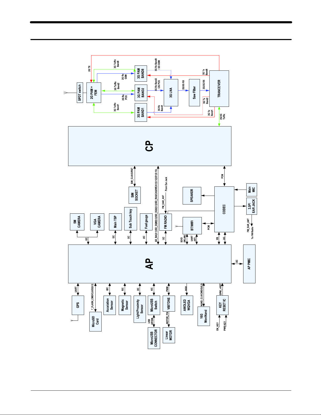
a-1. Block Diagram
8
3
Repair(HW REV0.8)
8-1
SAMSUNG Proprietary-Contents may change without notice
This Document can not be used without Samsung's authorization
Page 2
Level3Repair
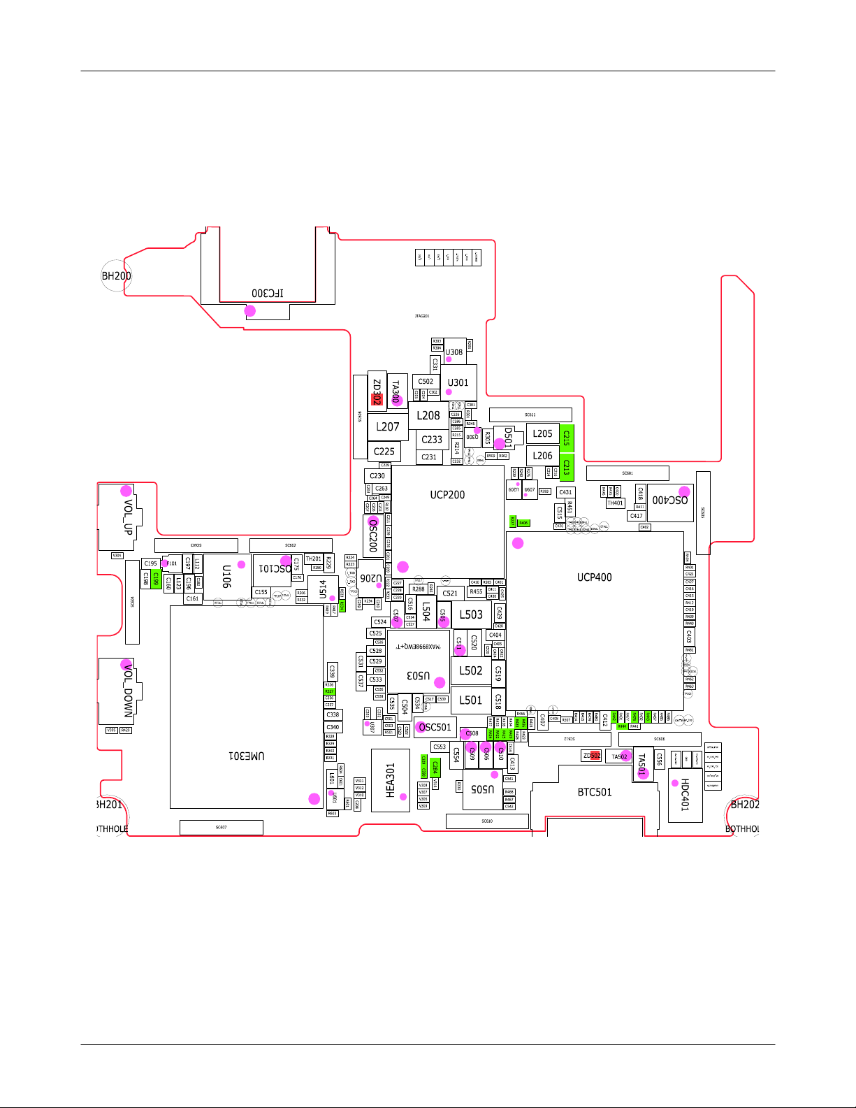
a-2. PCB Diagrams
8
a-2-1. Top
8
8-2
SAMSUNG Proprietary-Contents may change without notice
This Document can not be used without Samsung's authorization
Page 3
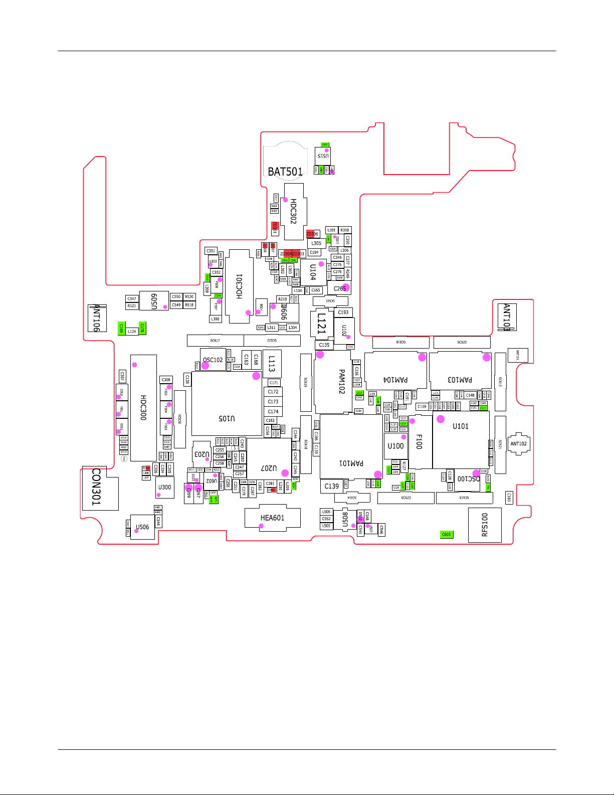
a-2-1. Bottom
8
Level3Repair
8-3
SAMSUNG Proprietary-Contents may change without notice
This Document can not be used without Samsung's authorization
Page 4
Level3Repair
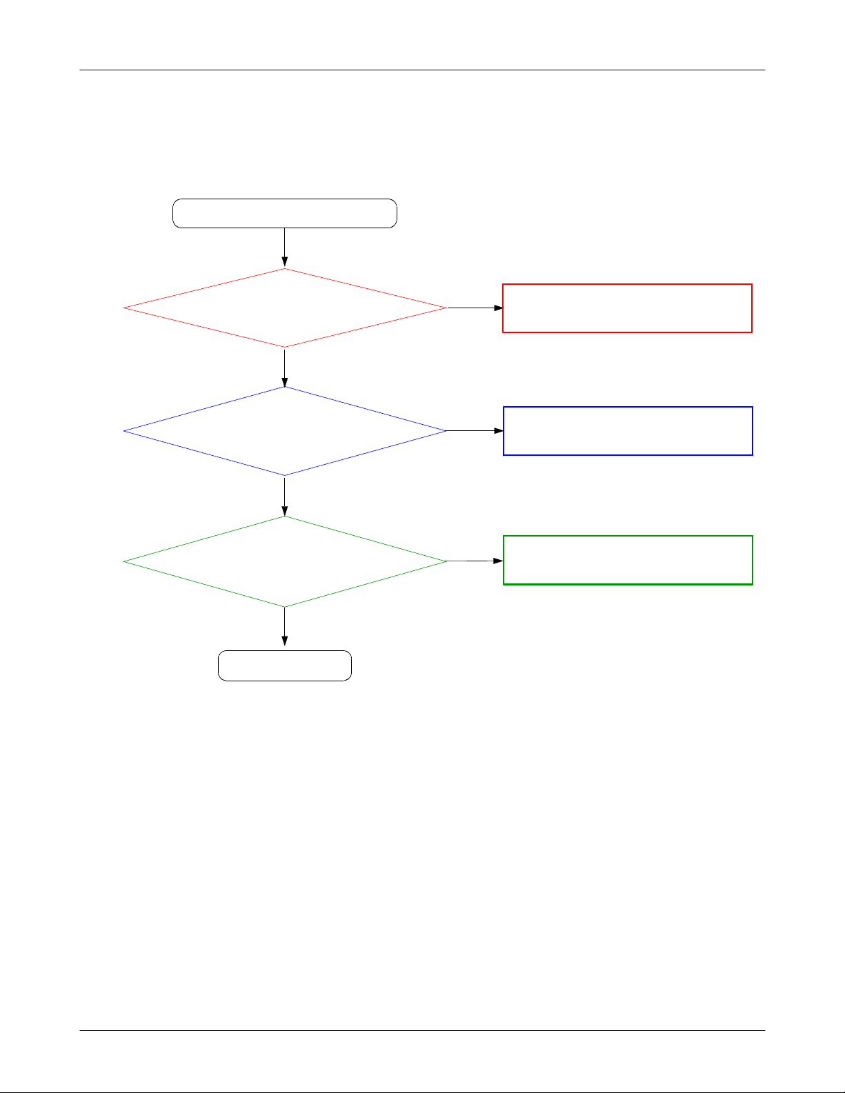
a-3. Flow Chart of Troubleshooting
8
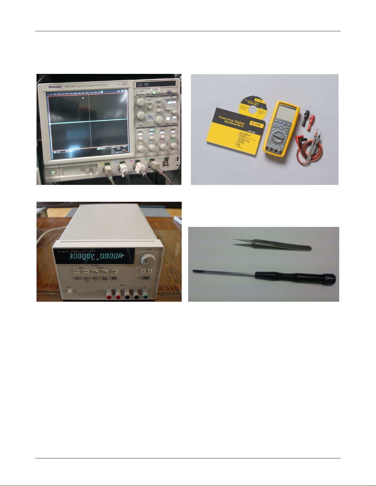
Equipments
Power Supply
Oscilloscope
Digital Multimeter
driver, Tweezer
+
8-4
SAMSUNG Proprietary-Contents may change without notice
This Document can not be used without Samsung's authorization
Page 5
Level3Repair
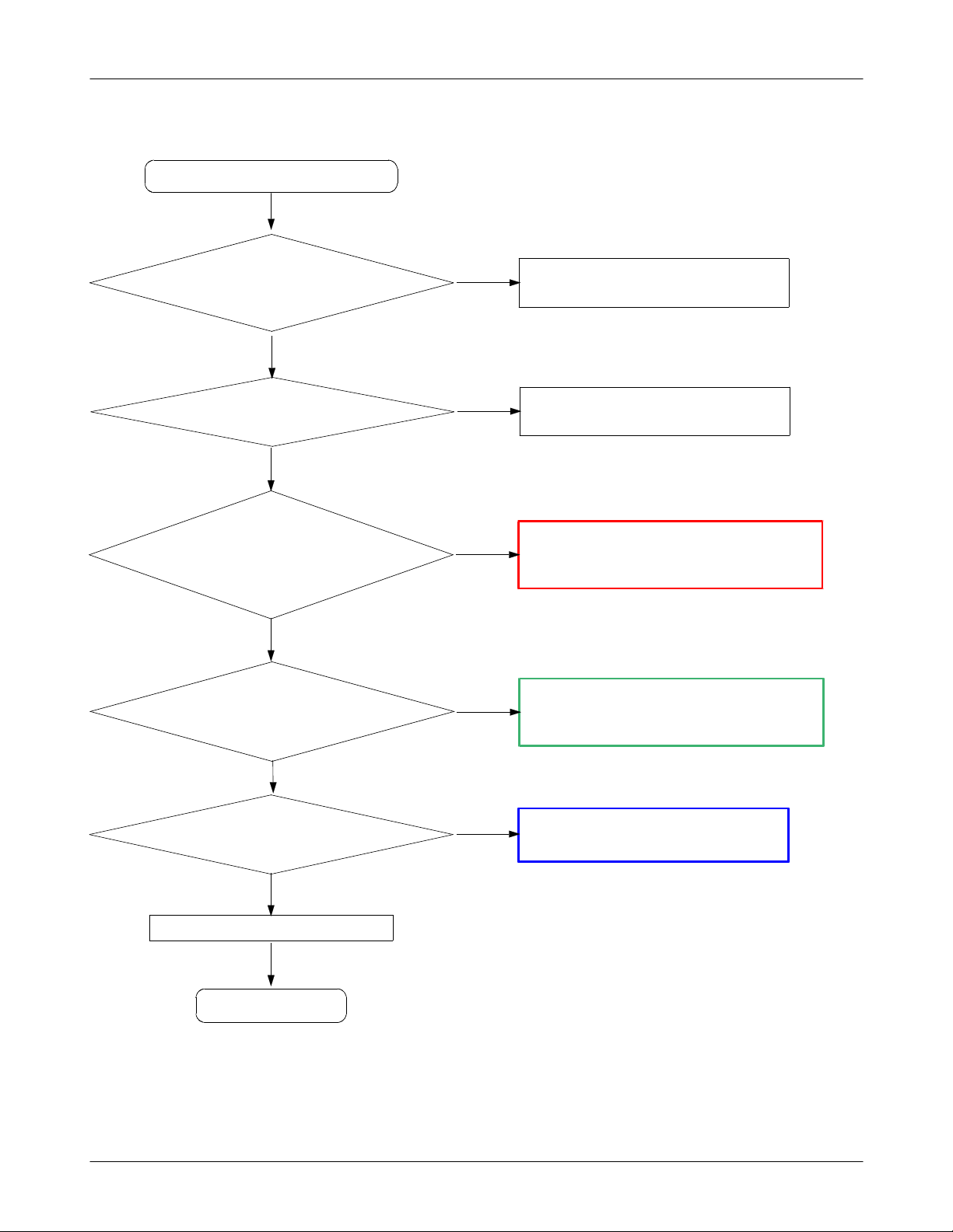
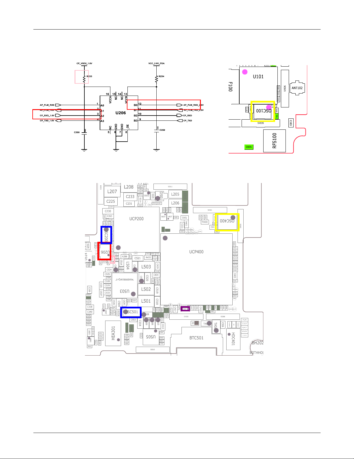
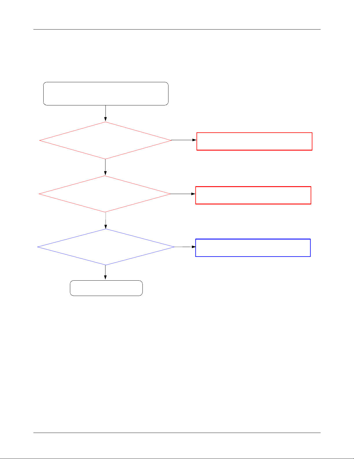
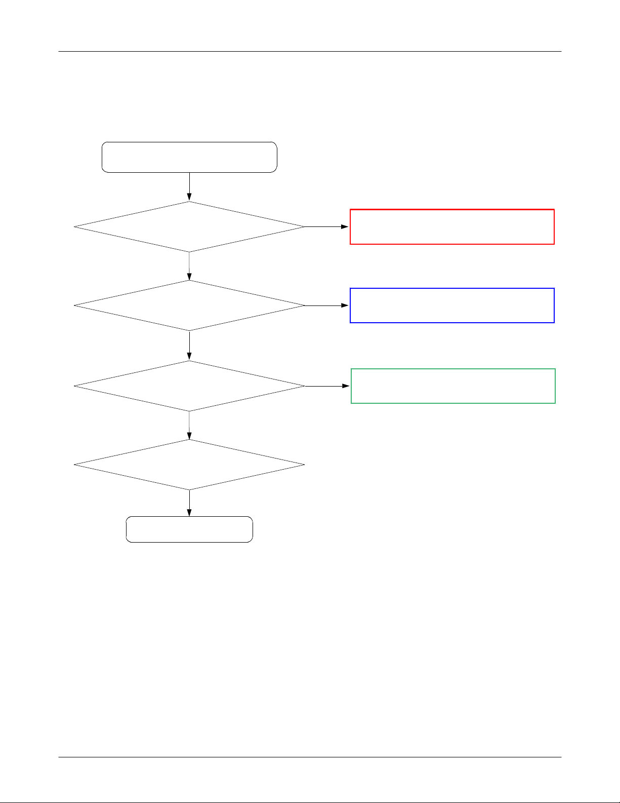
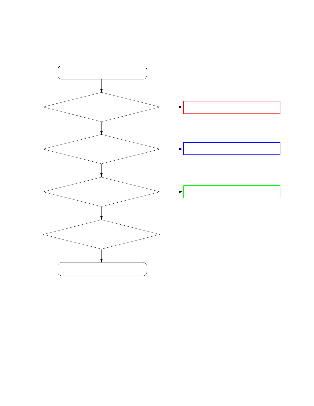
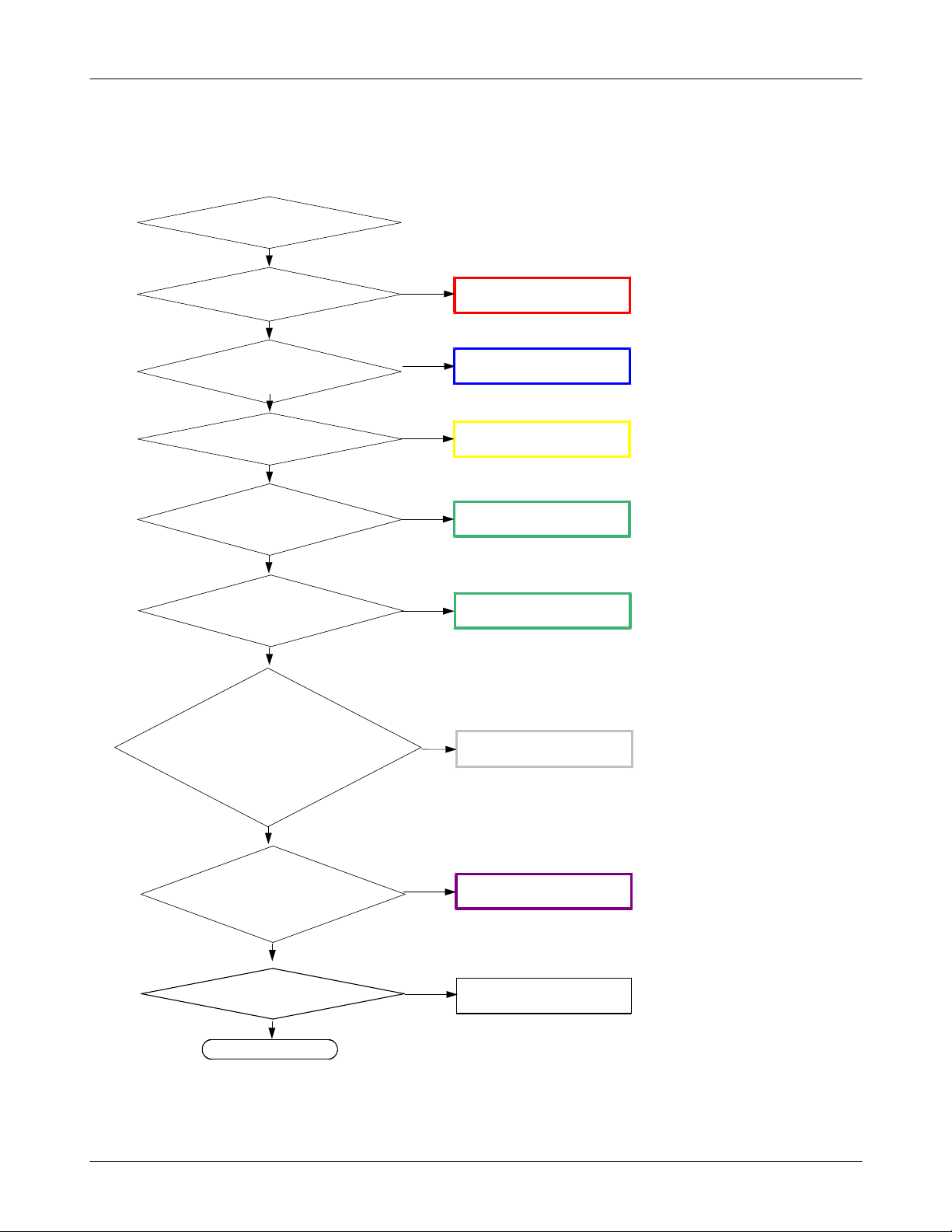
8a-3-1.
Power On
Power On'does not work
'
Check the Battery Voltage
is more than
check current consumption
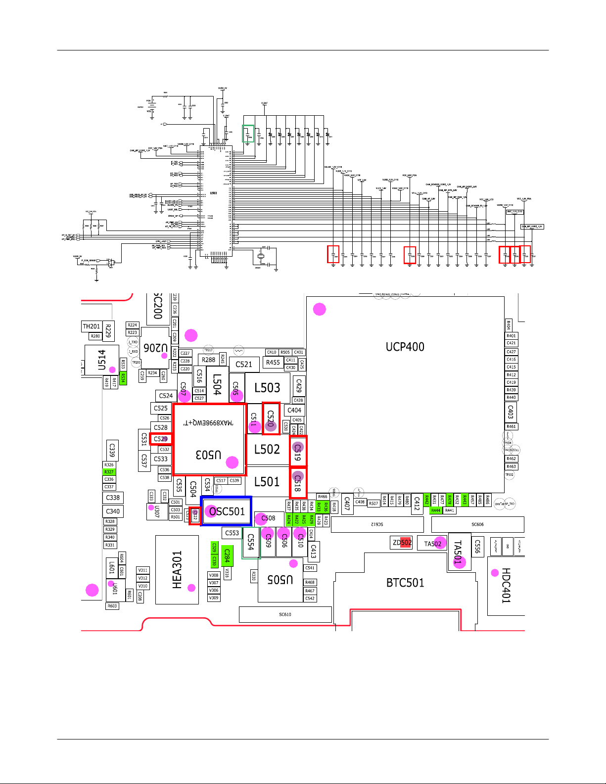
Check U503(PMIC) and
C518
(
C520>1.8V, C522,>
>=100
Power on voltage
V, C519
>1.2
>1.8
Yes
Yes
mA
Yes
V)
3.3V
1.2V
>1.1
V,
C529
No
No
No
Check the problem point(short, open, crack etc)
Change the Battery
Because of batt. power low)
(
Download again
and If PMIC has problem, change U503
Yes
Check Resistance Values of
C230, C231, C518, C554. Are
the values are less than
check the initial operation
ohm?
No
Check the Clock at
OSC501 that
Frequency is
Yes
Yes
END
100
32K
Yes
No
Replace capacitor or capacitors that has/have less
than
Resolder or Replace OSC501, C517 and
ohm resistance.
100
C539
8-5
SAMSUNG Proprietary-Contents may change without notice
This Document can not be used without Samsung's authorization
Page 6
Level3Repair
8-6
SAMSUNG Proprietary-Contents may change without notice
This Document can not be used without Samsung's authorization
Page 7
Level3Repair
8-7
SAMSUNG Proprietary-Contents may change without notice
This Document can not be used without Samsung's authorization
Page 8
Level3Repair
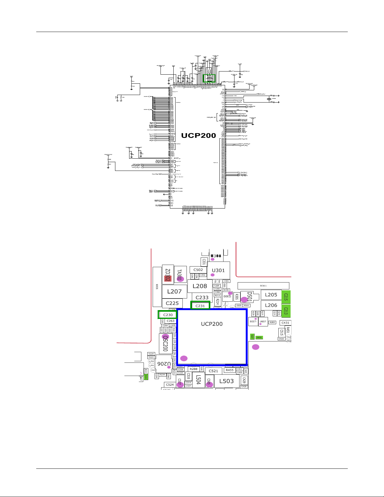
8a-3-2.
Initial
Initial Failure
Yes
The pin
swing properly
The pin
swing properly
AP_PS_HOLD(TP501) and
AP_N_RST_IN(R507)
lowHigh"?
"
There is
32.768
at OSC200 and OSC501
of U206
#1,2
1.8V
of U206=
#11,12
2.8V
Yes
Yes
KHz wave forms
Yes
=
and0V?
and0V?
=
No
check U206 and UCP400 and related parts(short,
No
if U503 has some problem, it is to be replaced)
(
No
Check U503(crack, open, etc)
Replace OSC
crack, etc)
200
and OSC501
R233
There are24MHz wave forms at
OSC400 and26MHz wave forms
at OSC100(C128)
LCD display OK?
Sound is OK?
>= 1.8
END
V?
Yes
Yes
Yes
Yes
No
Check UCP200 and related parts(short, crack,
No
Replace OSC
No
No
Check the LCD part(short, crack, etc)
Check the Audio Part(short, crack, etc)
etc)
and OSC100
400
8-8
SAMSUNG Proprietary-Contents may change without notice
This Document can not be used without Samsung's authorization
Page 9
Level3Repair
8-9
SAMSUNG Proprietary-Contents may change without notice
This Document can not be used without Samsung's authorization
Page 10
Level3Repair
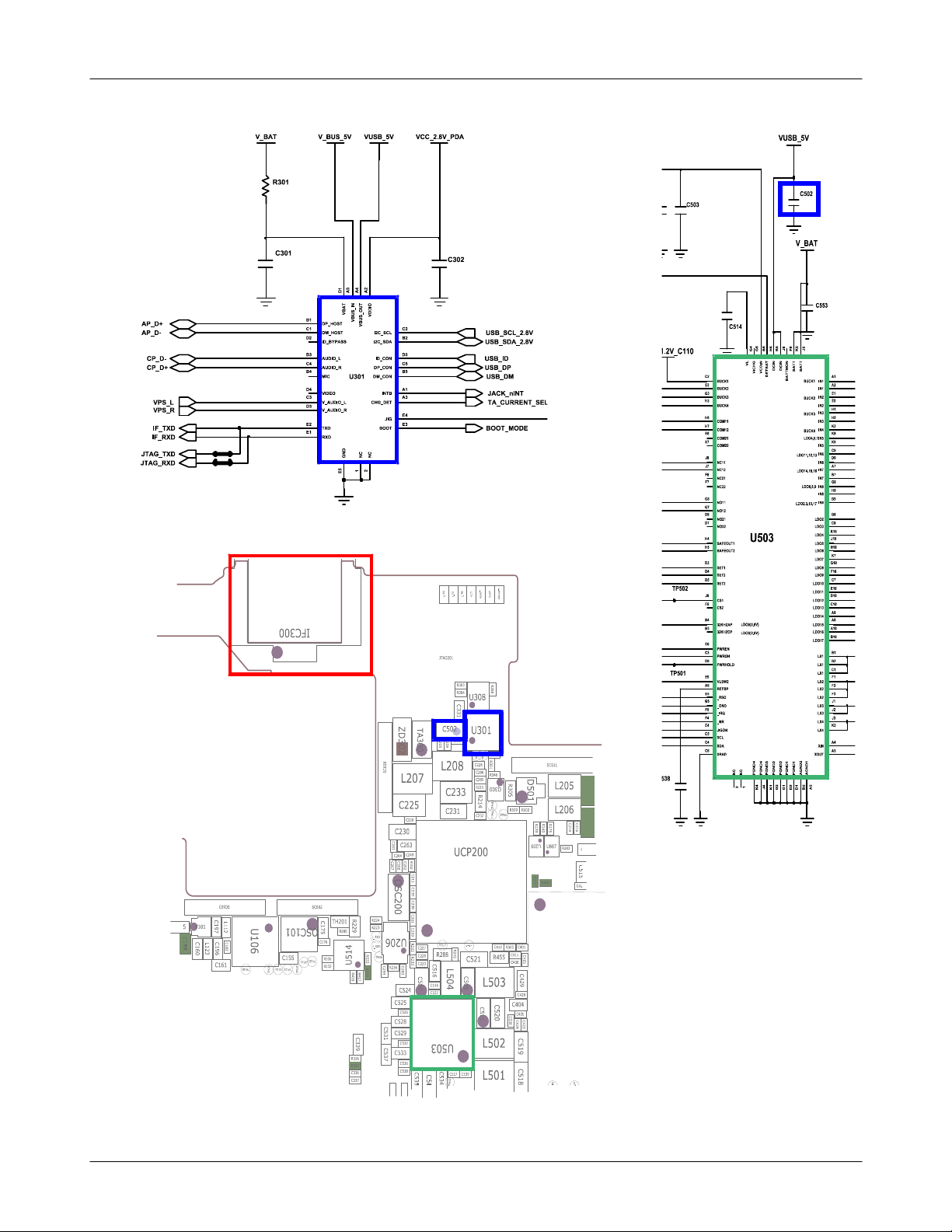
8a-3-3.
Charging Part
Check IFC300 pin#1whether
voltage reading is greater than
Check U503 DCIN whether
Abnormal charging part
Yes
4.9V
Yes
is measured
C502)
(
Yes
5V
No
No
Check the TA
TA may not be connected properly)
(
Resolder or Replace U301
Battery is charging?
Yes
END
No
Resolder or Replace U503
8-10
SAMSUNG Proprietary-Contents may change without notice
This Document can not be used without Samsung's authorization
Page 11
Level3Repair
8-11
SAMSUNG Proprietary-Contents may change without notice
This Document can not be used without Samsung's authorization
Page 12
Level3Repair
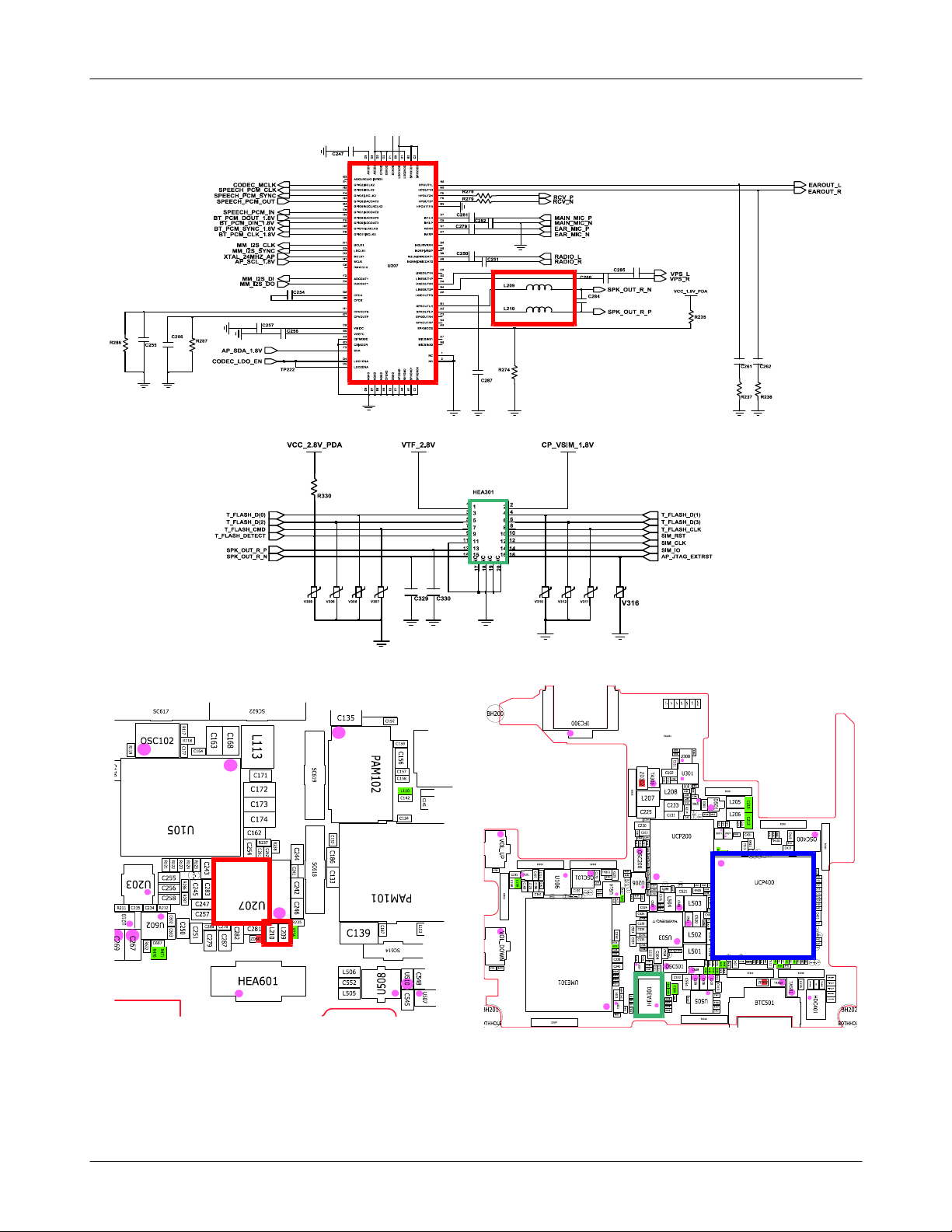
8a-3-4.
Sim Part
NO SIM
Yes
Check the connection of
the HEA301
Yes
Check the Sub PCB
Yes
END
No
Reconnect the Sub PCB
T_FLASH_D(0)
T_FLASH_D(2)
T_FLASH_DETECT
SPK_OUT_R_P
SPK_OUT_R_N
R330
VTF_2.8V
HEA301
1
3
5
7
9
111112
15
C
C
N
N
7
8
1
1
5
U
C539
C517
1
0
5
P
T
C553
C
3
2
C
9
2
8
C
3
4
3
0
V
3
1
6
2
2
4
4
6
6
8
8
10
10
12
C
C
N
N
0
9
1
2
C
5
1
L502
9
C
5
1
L501
8
R
R
4
4
3
3
5
7
R
R
4
4
2
2
C508
2
4
C
C
C
5
5
5
0
0
5
6
9
4
R
3
5
0
5
U
3
0
SC610
1
3
5
7
9
13 13 14 14
15 1616
C330
V307V306 V310
C329
C
3
3
9
C
5
3
C533
7
R326
R327
C336
C337
C
3
3
3
C338
U
3
0
C340
7
R328
R329
R340
R331
R
6
0
4
L
6
C
0
6
1
0
V311
1
V312
U
6
V310
0
R
C
1
6
2
0
0
1
8
R603
0
3
C532
C536
C
C
C538
C
5
5
3
5
3
4
5
0
C
4
3
3
2
C501
C
C
C503
5
5
OSC501
2
2
2
3
R501
1
0
3
A
V308
E
V307
H
V306
V309
CP_VSIM_1.8VVCC_2.8V_PDA
T_FLASH_D(1)
T_FLASH_D(3)
T_FLASH_CLKT_FLASH_CMD
SIM_RST
SIM_CLK
SIM_IO
AP_JTAG_EXTRST
V311V309
V312V308
R
R
R
4
4
4
3
3
3
4
8
3
R
R
R
4
4
4
2
2
2
5
9
8
C
4
C
1
4
5
1
0
C
4
1
3
C541
R468
R467
C542
V316
8-12
SAMSUNG Proprietary-Contents may change without notice
This Document can not be used without Samsung's authorization
Page 13
Level3Repair
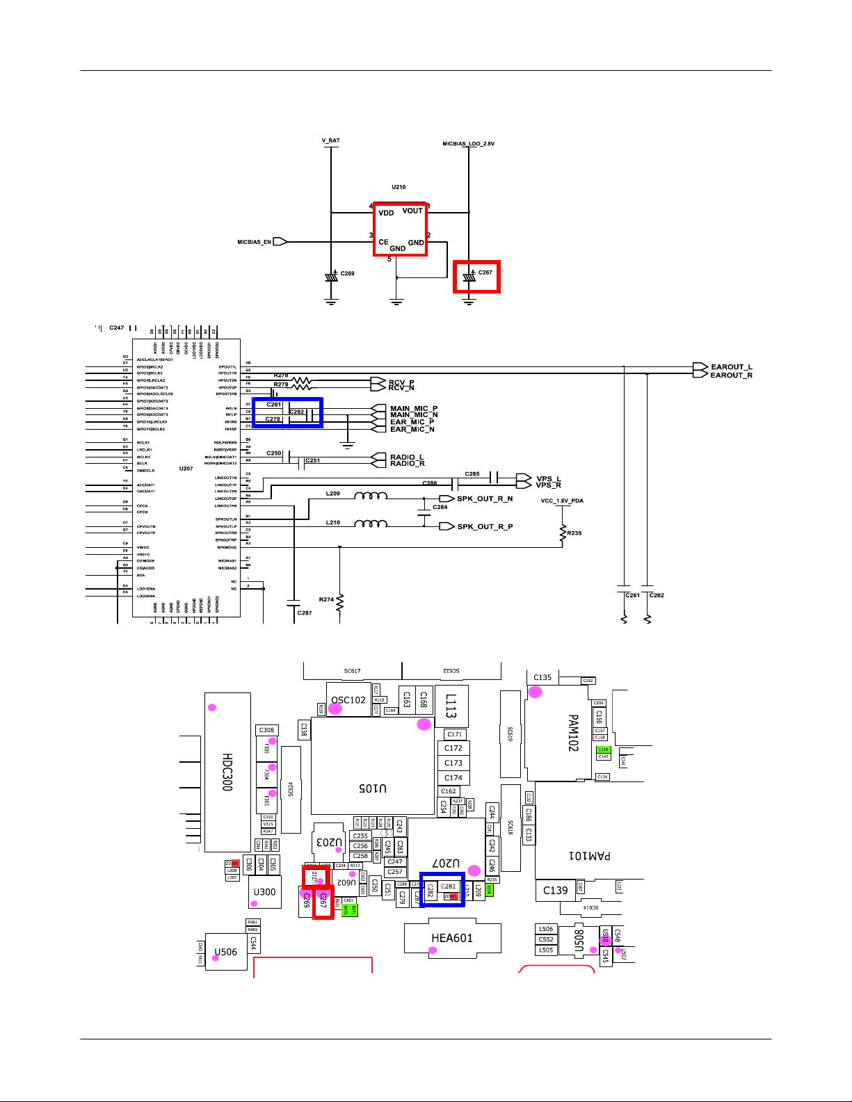
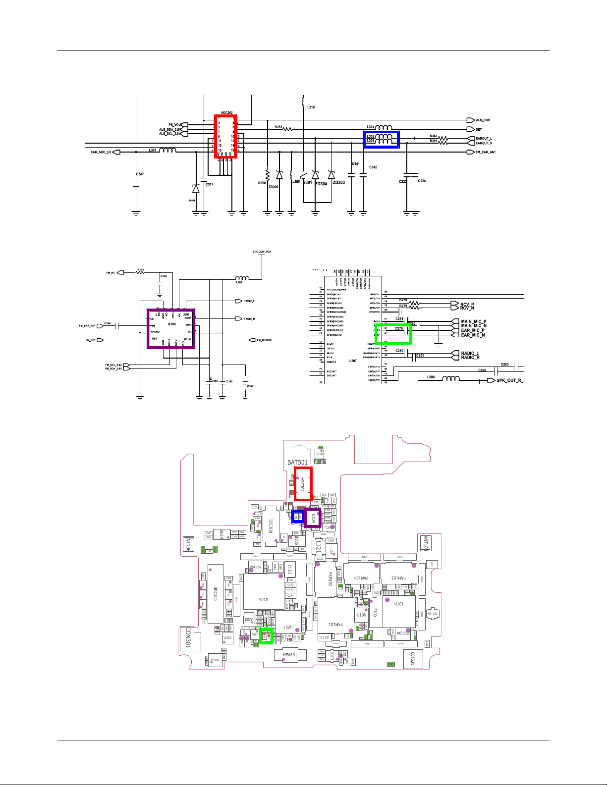
8a-3-5.
Microphone Part
Check main microphone function
in voice call receiver mode
Yes
Check Sub-Touch Module
FPCB where main Mic is
placed for any damage(Tear
in FPC, etc)
Yes
Check the voltage at C267
2.8V
No
=
No
Change the Sub-Touch Module
Resolder or replace U210
Yes
Check component soldering
statuses of C281, C282
Yes
END
No
Resolder or replace C281, C282
8-13
SAMSUNG Proprietary-Contents may change without notice
This Document can not be used without Samsung's authorization
Page 14
Level3Repair
8-14
SAMSUNG Proprietary-Contents may change without notice
This Document can not be used without Samsung's authorization
Page 15
Level3Repair
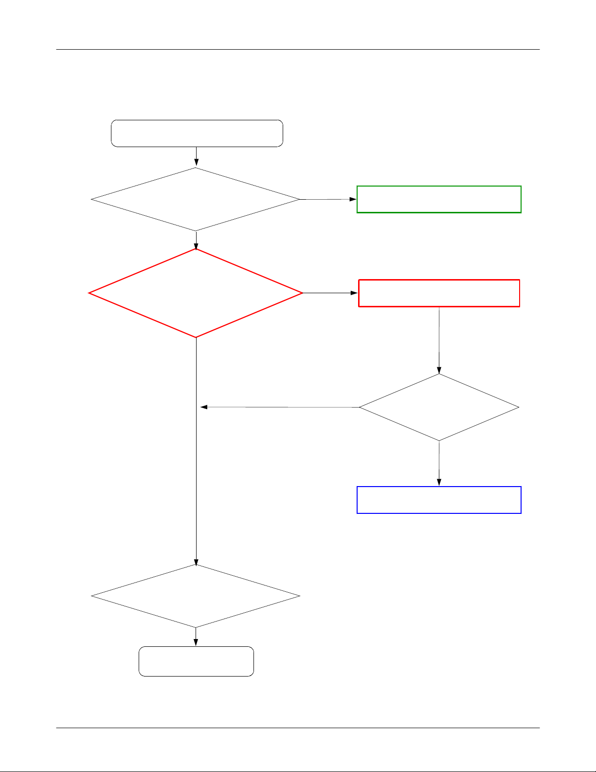
8a-3-6.
Speaker Part
Play MP3 with maximum volume level.
Check speaker function.
Yes
Check the connection of
HEA301
Yes
Check signals on L209,
L210
Yes
No
No
Reconnect HEA301
Resolder or replace U207
Replace the speaker
module
Yes
END
Yes
Check signals on
L209, L210 again
No
Replace UCP400
8-15
SAMSUNG Proprietary-Contents may change without notice
This Document can not be used without Samsung's authorization
Page 16
Level3Repair
8-16
SAMSUNG Proprietary-Contents may change without notice
This Document can not be used without Samsung's authorization
Page 17
Level3Repair
8a-3-7.
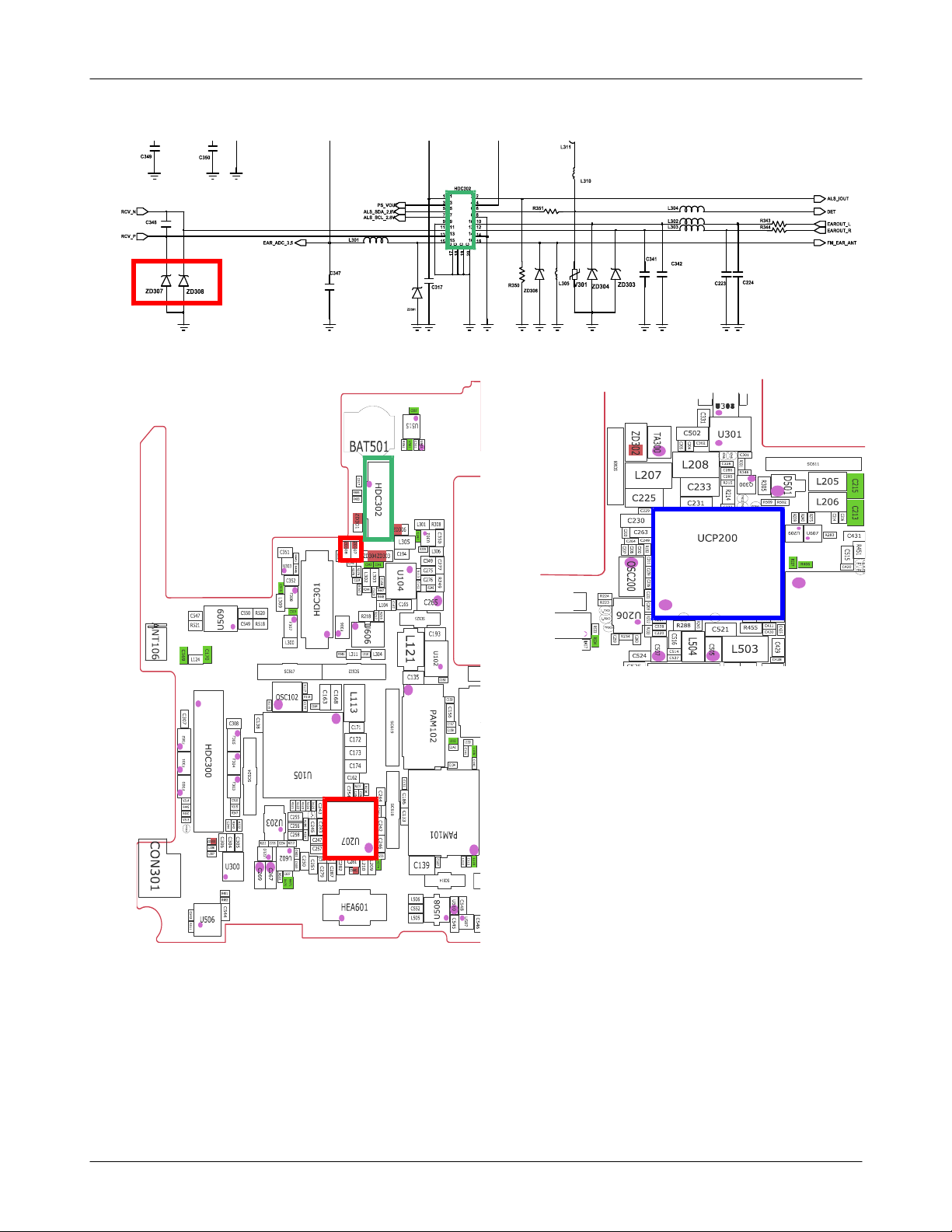
Receiver Part
Check receiver function in voice call receiver
mode
Yes
Check the signals at ZD307,
Check the signals at ZD307,
Check the connection of
ZD308
Yes
ZD308 again
Yes
HDC302
No
No
No
Resolder or replace U207
Resolder or replace UCP200
Reconnect HDC302
Yes
Replace the Receiver-Earjack
Ass'y
Yes
END
8-17
SAMSUNG Proprietary-Contents may change without notice
This Document can not be used without Samsung's authorization
Page 18
Level3Repair
8-18
SAMSUNG Proprietary-Contents may change without notice
This Document can not be used without Samsung's authorization
Page 19
Level3Repair
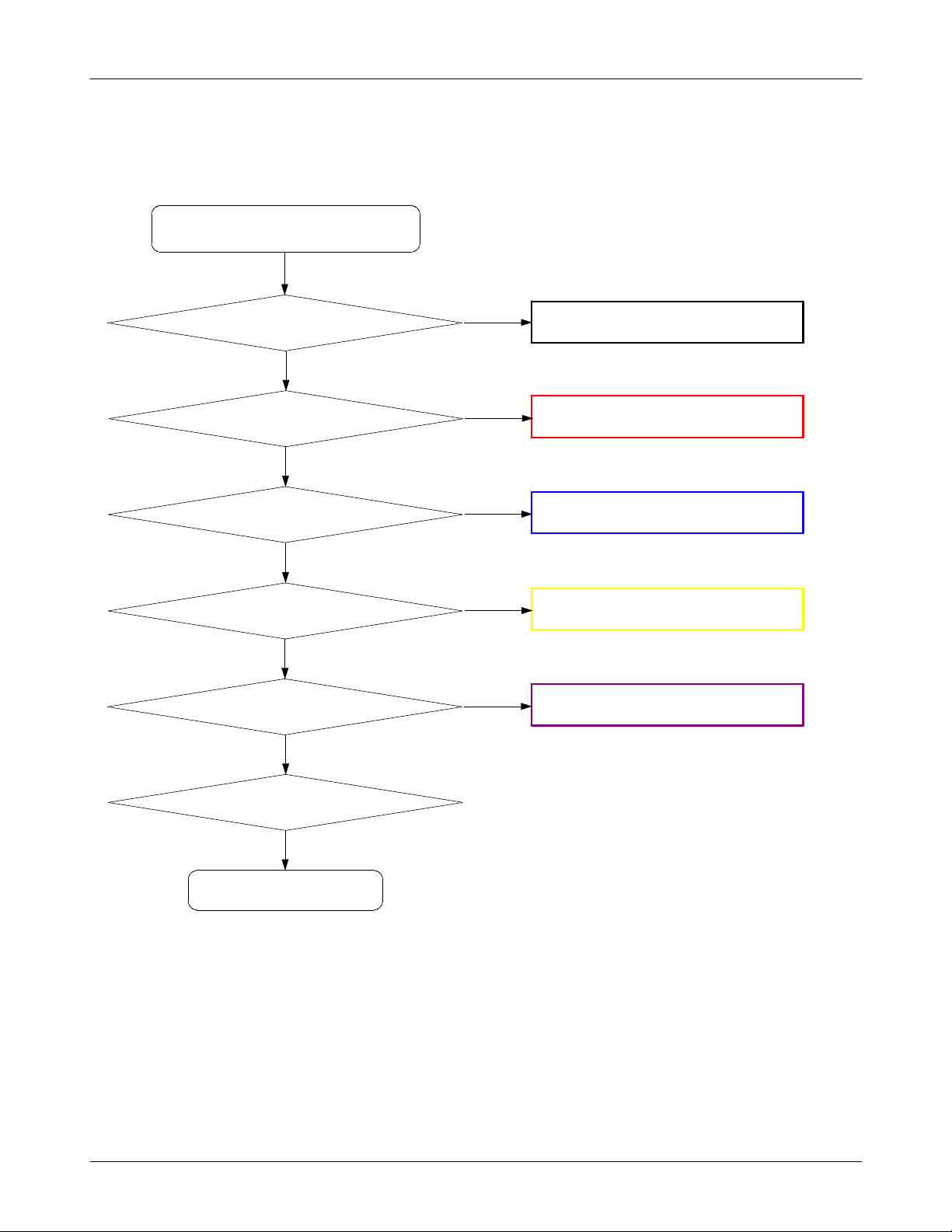
8a-3-8.
BT/WIFI
Check the Voltage on C162
BT/WiFi is not working
Check BT or WiFi function
Check
ON
Yes
2.8V
Yes
MHz Clock at
38.4
C177
Yes
No
=
No
No
etc.(If U503 has some problem, it needs to
Enable BT or WiFi Function
Check AP PMIC(U503) for Crack, Open or
be replaced)
Check OSC
102
heck the Voltage on L113
C
Check the Status of C138,
Resolder or Replace U105
1.2V
Yes
L124, ANT106
Yes
Yes
END
=
No
No
Resolder or change L113
Resolder or Replace C138, L124, ANT106
8-19
SAMSUNG Proprietary-Contents may change without notice
This Document can not be used without Samsung's authorization
Page 20
Level3Repair
8-20
SAMSUNG Proprietary-Contents may change without notice
This Document can not be used without Samsung's authorization
Page 21
Level3Repair
8a-3-9.
FM RADIO
Check the Audio Signal at
Check the Audio signal at
FM Radio does not work
Yes
Check the connection of
HDC302
Yes
L302, L303
Yes
C250, C251
No
No
No
Connect Earjack Ass'y correctly to HDC302
Check Earphone
Check Audio Codec IC(U207)
Yes
CChange U104
Yes
END
8-21
SAMSUNG Proprietary-Contents may change without notice
This Document can not be used without Samsung's authorization
Page 22
Level3Repair
8-22
SAMSUNG Proprietary-Contents may change without notice
This Document can not be used without Samsung's authorization
Page 23
Level3Repair
8a-3-10.
LCD
LCD is still off after PWR ON
Check the connection of
Check the soldering status of
Check VCC_3.0V_LCD
3.0V (
1.8V (
HDC300
EMI Filters F300~F305
C537), VLCD_1.8V
C307), V_BAT
C308)
(
Yes
Yes
Yes
=
=
>3.4V
No
No
No
Reconnect the HDC300
Resolder EMI Filters
Check PMIC(U503)
Yes
Replace LCD Module
Yes
END
8-23
SAMSUNG Proprietary-Contents may change without notice
This Document can not be used without Samsung's authorization
Page 24
Level3Repair
8-24
SAMSUNG Proprietary-Contents may change without notice
This Document can not be used without Samsung's authorization
Page 25
Level3Repair
8a-3-11.
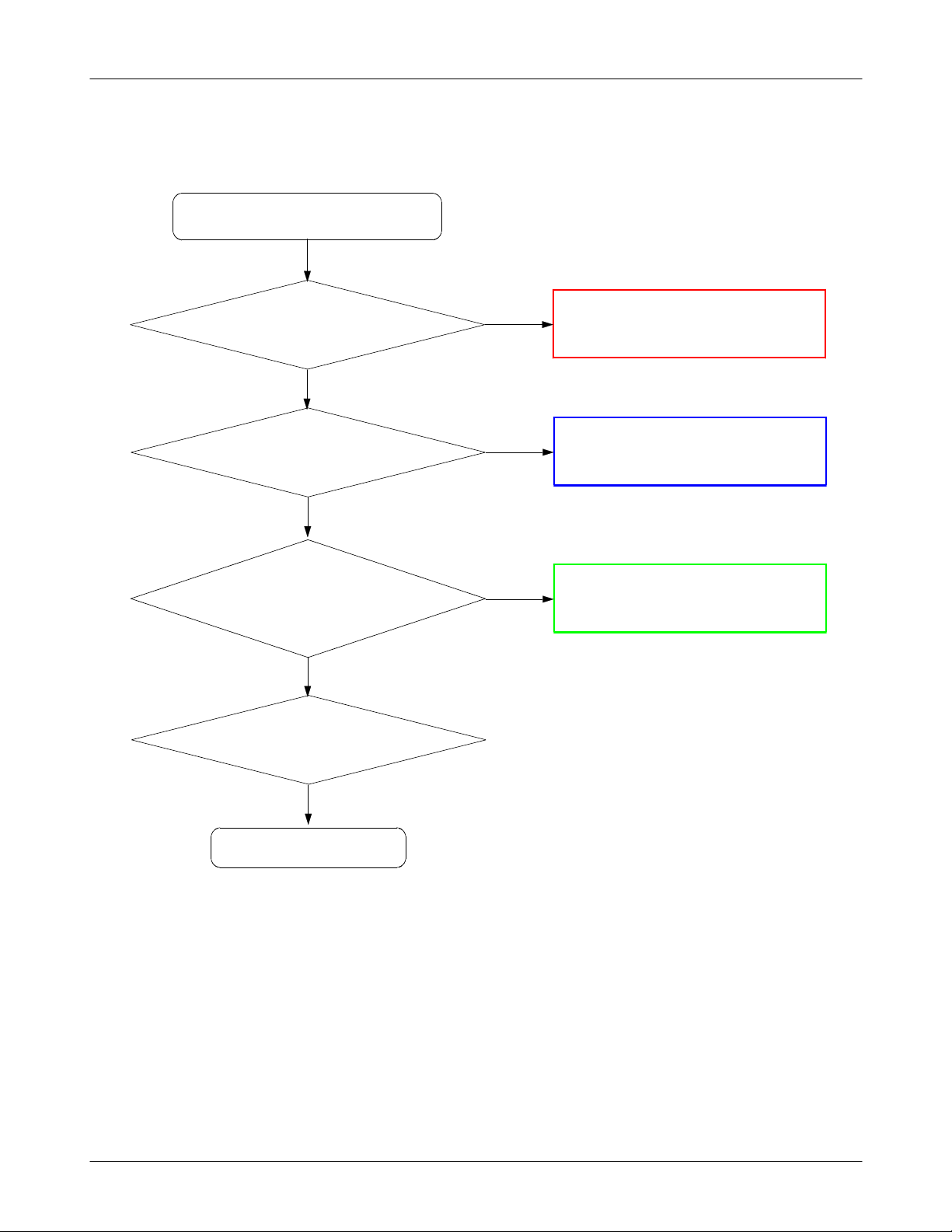
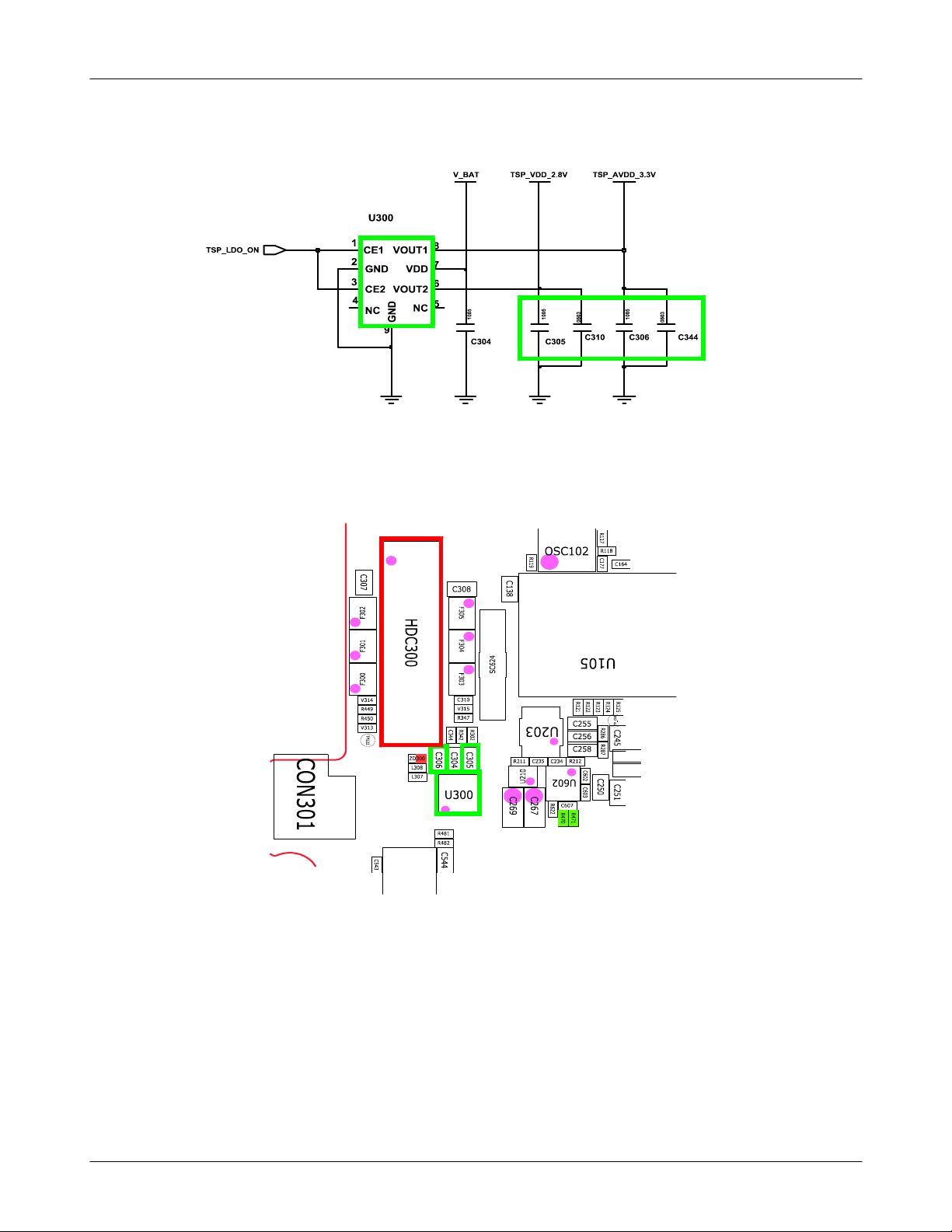
TSP
Touch Screen does not work
Yes
Check LCD Connector on
Main PBA
Yes
Check the TSP Connector on
LCD Module
U300 Pin
C310) and Pin
6=2.8V(
C306, C344)
(
Yes
C305,
8=3.3V
No
No
No
Reconnect the HDC300
Reconnect TSP Connector
Resolder or Replace U300
Yes
Replace LCD Module
Yes
END
8-25
SAMSUNG Proprietary-Contents may change without notice
This Document can not be used without Samsung's authorization
Page 26
Level3Repair
8-26
SAMSUNG Proprietary-Contents may change without notice
This Document can not be used without Samsung's authorization
Page 27
Level3Repair
8a-3-12. 5M
CAM
Camera" function does not work
"
Yes
Check the Camera
connector on Main PBA
Yes
Check the voltage
C531,C533,C535
C534, C536
C532, C521
C352
=1.8
=1.2V
=2.8V
=2.8
V,
No
V,
No
Reconnect the HDC301
Resolder U503, U303 or change PBA
Yes
Check F308 Pin1is24MHz
Yes
Replace the camera module
END
No
Check UCP400 related to24MHz
8-27
SAMSUNG Proprietary-Contents may change without notice
This Document can not be used without Samsung's authorization
Page 28
Level3Repair
T
T
T
L
NI
NI
NI
N
G
T
T
V
A
H
O
C
C
O
A
A
B
C
M
D
D
C
I
B
B
T
T
V
V
E
T
D
A1
A
B
BUCK1
IN1
A2
IN1
E1
IN2
BUCK2
E2
IN2
H1
IN3
BUCK3
H2
IN3
K2
IN4
BUCK4
K8
LDO4,5,7
IN5
K9
IN5
C9
IN6
LDO11,12,13
D9
IN6
A7
IN7
LDO14,15,16
B7
IN7
G9
LDO6,8,9
IN8
H9
IN8
B9
IN9
LDO2,3,10,17
B8
LDO2
C8
LDO3
K10
LDO4
U503
4
D
N
C
C
G
N
N
P
4
2
1
K
J10
LDO5
H10
LDO6
K7
LDO7
G10
LDO8
F10
LDO9
C7
LDO10
E10
LDO11
D10
LDO12
C10
LDO13
A6
LDO14
A8
LDO15
A10
LDO16
B10
LDO17
B1
LX1
B2
LX1
C1
LX1
F1
LX2
F2
LX2
F3
LX2
J1
LX3
J2
LX3
J3
LX4
K3
LX4
A4
XIN
A3
XOUT
3
4
2
2
1
1
2
1
D
D
D
D
D
D
D
D
N
N
N
N
N
N
N
N
G
G
G
G
G
G
G
G
P
P
P
P
P
P
A
A
1
2
1
5
1
2
5
4
J
D
B
K
D
A
G
G
VALIVE_1.2V_C110
0.8V~1.3V UP TO 10mA
VUSB_1.1V_C110
VADC_3.3V_C110
VTF_2.8V
0.8V~1.3V UP TO 50mA
1.6V~3.6V UP TO 300mA
1.6V~3.6V UP TO 300mA
C524 C535
C522
1.6V~3.6V UP TO 150mA
C525
1.6V~3.6V UP TO 150mA
C526
VLCD_1.8V
3.0V~3.6V UP TO 150mA
VUSB_3.3V_C110
VDAC_3.3V_C110
C527 C528
VCC_2.8V_PDA
VPLL_1.2V_C110
C529
CAM_SENSOR_CORE_1.2V
CAM_AF_2.8V
CAM_ISP_SYS_2.8V
CAM_ISP_RAM_1.8V
C532
C533
CAM_ISP_HOST_2.8V
CAM_SENSOR_IO_1.8V
C534
VCC_3.0V_LCD
C536
L502
L503
L504
C537
VARM_1.2V_C110
VINT_1.1V_C110
C518
VCC_1.8V_PDA
CAM_ISP_CORE_1.2V
C519
C521
C520
CAM_IO_EN
V_BAT
C351
U303
VDD4VOUT
3
CE
5
GND
D
N
G
CAM_SENSOR_A2.8V
1
2
C352
CAM_MCLK_F
CAM_HSYNC_F
CAM_VSYNC_F
CAM_PCLK
F308
OUT1
OUT2
OUT3
OUT4
GND
5
6
7
8
1
IN1
2
IN2
3
IN3
4
IN4
GND
C315
L309
CAM_MCLK
CAM_HSYNC
CAM_VSYNC
CAM_PCLK_F
910
8-28
SAMSUNG Proprietary-Contents may change without notice
This Document can not be used without Samsung's authorization
Page 29
Level3Repair
8a-3-13.
GSM
RX
850
NORMAL CONDITION
catch the channel?
NO
Check C115
Check the Voltage at
C186=V_BAT
Check C126, L107,C125
Check component
soldering status OK at
-65
F100
dBm
-65
NO
YES
?
YES
YES
dBm
?
YES
NO
NO
NO
CHECK soldered
RFS100, L103,C115,L118
resolder or change
PAM101, C186
resolder or change
C126, L107,C125
resolder or change
F100
Check F100 PIN
Check the voltage at
R100=V_BAT
{
C110, C264
&{
C111,C112,C233
&{
C109,C263
&{
&{
Check the freq. at C128
GSM850 Receiver is O.K?
C112
-65
=1.8GV?}
MHz
:26
END
dBm
YES
= 2.85V ?}
=1.8
= 2.85V ?}
YES
?
YES
8,9
NO
?}
V?}
YES
NO
NO
NO
resolder or change
F100
resolder or change
UCP200
change or resolder
OSC100
resolder or change
UCP200
8-29
SAMSUNG Proprietary-Contents may change without notice
This Document can not be used without Samsung's authorization
Page 30
Level3Repair
8-30
SAMSUNG Proprietary-Contents may change without notice
This Document can not be used without Samsung's authorization
Page 31

Level3Repair
8a-3-14.
GSM
1800
RX
NORMAL CONDITION
catch the channel?
NO
Check C115
Check the Voltage at
C186=V_BAT
Check C140, L108
Check component
soldering status OK at
-65
dBm
F100
-65
NO
YES
YES
YES
dBm
?
?
?
YES
NO
NO
NO
CHECK soldered
RFS100, L103,C115,L118
resolder or change
PAM101, C186
resolder or change
C140, L108
resolder or change
F100
Check F100 PIN
Check the voltage at
R100=V_BAT
{
C110, C264
&{
C111,C112,C233
&{
C109,C263
&{
C112
&{
Check the freq. at C128
:26
GSM850 Receiver is O.K?
14, 15
dBm
-65
YES
= 2.85V ?}
=1.8
= 2.85V ?}
=1.8GV?}
YES
MHz
?
YES
NO
?}
V?}
YES
NO
NO
NO
resolder or change
F100
resolder or change
UCP200
change or resolder
OSC100
resolder or change
UCP200
END
8-31
SAMSUNG Proprietary-Contents may change without notice
This Document can not be used without Samsung's authorization
Page 32

Level3Repair
8-32
SAMSUNG Proprietary-Contents may change without notice
This Document can not be used without Samsung's authorization
Page 33

Level3Repair
8a-3-15.
WCDMA Band1 RX
NORMAL CONDITION
catch the channel?
NO
Check C115
Check the Voltage at
C186=V_BAT
PAM101 CHECK
pin7or C141, L109
Check component soldering
status OK at PAM104, C185,
L120, L102, C114
-65
dBm
-65
NO
YES
?
YES
dBm
CONTINUOUS RX ON
RF INPUT
AMP
:-50
?
?
?
YES
NO
NO
NO
CHECK soldered
RFS100, L103, C115, L118
resolder or change
C186, PAM101
resolder or change
PAM101, C141, L109
resolder or change
PAM104, C185,
L120, L102, C114
: 10700
dBm
CH
YES
Check component soldering
status OK at
U100, F100
F100 PIN
&{
&{
&{
Check the freq. at OSC100
WCDMA BAND1 Receiver is O.K?
10, 11-65
Check the voltage at
R100=V_BAT
{
C110, C264
C111,C112,C233
C109,C263
C112
&{
:26
END
YES
= 2.85V ?}
= 2.85V ?}
=1.8GV?}
YES
MHz
?
YES
YES
?
?}
=1.8
dBm
V?}
NO
NO
NO
NO
resolder or change
U100, F100
resolder or change
UCP200
change or resolder
OSC100
resolder or change
UCSP200
8-33
SAMSUNG Proprietary-Contents may change without notice
This Document can not be used without Samsung's authorization
Page 34

Level3Repair
8-34
SAMSUNG Proprietary-Contents may change without notice
This Document can not be used without Samsung's authorization
Page 35

Level3Repair
8a-3-16.
WCDMA Band2/GSM1900 RX
NORMAL CONDITION
catch the channel?
NO
Check C115
Check the Voltage at
C186=V_BAT
PAM101 CHECK
pin9or C127, C143, L111
status OK at PAM103, C113,
-65
Check component soldering
L101, C101
Check C131
dBm
-65
-65
NO
YES
?
YES
dBm
dBm
?
?
?
?
YES
NO
NO
NO
CHECK soldered
RFS100, L103, C115, L118
resolder or change
C186, PAM101
resolder or change
PAM101, C127, C143, L111
resolder or change
PAM103, C113, L101, C101,
C131
CONTINUOUS RX ON
RF INPUT
AMP
:-50
: 9800
dBm
CH
YES
Check component soldering
status OK at
U100, F100
F100 PIN
&{
&{
&{
Check the freq. at OSC100
WCDMA BAND2, PCS1900 Receiver is O.K?
12, 13-65
Check the voltage at
R100=V_BAT
{
C110, C264
C111,C112,C233
C109,C263
C112
&{
:26
END
YES
= 2.85V ?}
= 2.85V ?}
=1.8GV?}
YES
MHz
?
YES
YES
?
?}
=1.8
dBm
V?}
NO
NO
NO
NO
resolder or change
U100, F100
resolder or change
UCP200
change or resolder
OSC100
resolder or change
UCSP200
8-35
SAMSUNG Proprietary-Contents may change without notice
This Document can not be used without Samsung's authorization
Page 36

Level3Repair
8-36
SAMSUNG Proprietary-Contents may change without notice
This Document can not be used without Samsung's authorization
Page 37

Level3Repair
8a-3-17.
WCDMA Band8/GSM900 RX
NORMAL CONDITION
catch the channel?
NO
Check C115
Check the Voltage at
C186=V_BAT
PAM101 CHECK
pin5or C142, L110
-65
Check component soldering
status OK at PAM102, C122,
L106, L105, C121
Check C116
dBm
-65
-65
NO
YES
?
YES
dBm
dBm
?
?
?
?
YES
NO
NO
NO
CHECK soldered
RFS100, L103, C115, L118
resolder or change
C186, PAM101
resolder or change
PAM101, C142, L110
resolder or change
PAM102, C122, L106, L105,
C121, C116
CONTINUOUS RX ON
RF INPUT
AMP
:-50
: 9800
dBm
CH
YES
Check component soldering
status OK at
U100, F100
F100 PIN
Check the voltage at
R100=V_BAT
{
C110, C264
&{
C111,C112,C233
&{
C109,C263
&{
C112
&{
Check the freq. at OSC100
:26
WCDMA BAND8, GSM900 Receiver is O.K?
END
?
6, 7-65
YES
= 2.85V ?}
=1.8
= 2.85V ?}
=1.8GV?}
YES
MHz
?
YES
YES
dBm
?}
V?}
NO
NO
NO
NO
resolder or change
U100, F100
resolder or change
UCP200
change or resolder
OSC100
resolder or change
UCSP200
8-37
SAMSUNG Proprietary-Contents may change without notice
This Document can not be used without Samsung's authorization
Page 38

Level3Repair
8-38
SAMSUNG Proprietary-Contents may change without notice
This Document can not be used without Samsung's authorization
Page 39

Level3Repair
8a-3-18.
GSM
GSM900
850/
PAM101 PIN1:About
dBm
30
?
YES
Check the Voltage at
C186,C187,C139
V_BAT
?
YES
Check C132 about
Check PAM101 pin
?@MSR
ok?
4
YES
dBm
YES
TX
=
2V
25
NO
NO
NO
NO
CHECK soldered
RFS100, L103,C115,L118,
C183, ANT102
resolder or change
PAM101, C186, C187, C189
resolder or change
U101
resolder or change
U101
CONTINOUS TX ON CONDITION
TX POWER DAC:
APPLIED
GSM850 CH
GSM900 CH
RBW
: 100
VBW
: 100
SPAN
:10
REF LEV.
ATT.
:20
14500
KHz
KHz
MHz
:10
dB
: 190
:62
dBm
CODE
Check the voltage at
R100=V_BAT
{
C110, C264
&{
C111,C112,C233
&{
C109,C263
&{
C112
&{
Check the freq. at C128
GSM850/900 Transmitter is O.K?
=1.8GV?}
:26
END
= 2.85V ?}
= 2.85V ?}
YES
MHz
?
YES
?}
=1.8
V?}
YES
NO
NO
NO
resolder or change
UCP200
change or resolder
OSC100
resolder or change
UCP200
8-39
SAMSUNG Proprietary-Contents may change without notice
This Document can not be used without Samsung's authorization
Page 40

Level3Repair
8a-3-19.
DCS/PCS
PAM101 PIN1:About
Check the Voltage at
Check C132 about
Check PAM101 pin
TX
dBm
27
?
YES
C186,C134,C139
V_BAT
?
YES
ok?
YES
dBm
4
?@MSR
YES
=
1.8 V
25
NO
NO
NO
NO
CHECK soldered
RFS100, L103,C115,L118,
C183, ANT102
resolder or change
PAM101, C186, C134, C139
resolder or change
U101
resolder or change
U101
CONTINOUS TX ON CONDITION
TX POWER DAC:
APPLIED
GSM850 CH
GSM900 CH
RBW
: 100
VBW
: 100
SPAN
:10
REF LEV.
ATT.
:20
14500
KHz
KHz
MHz
:10
dB
: 190
:62
dBm
CODE
Check the voltage at
R100=V_BAT
{
C110, C264
&{
C111,C112,C233
&{
C109,C263
&{
C112
&{
Check the freq. at C128
DCS/PCS Transmitter is O.K?
=1.8GV?}
:26
END
= 2.85V ?}
= 2.85V ?}
YES
MHz
?
YES
?}
=1.8
V?}
YES
NO
NO
NO
resolder or change
UCP200
change or resolder
OSC100
resolder or change
UCP200
8-40
SAMSUNG Proprietary-Contents may change without notice
This Document can not be used without Samsung's authorization
Page 41

Level3Repair
8-41
SAMSUNG Proprietary-Contents may change without notice
This Document can not be used without Samsung's authorization
Page 42

Level3Repair
8a-3-20.
WCDMA BAND1
Check PAM101 PIN1
About22dBm
Check the Voltage at
C186=V_BAT
Check C141, L109
About22dBm
Check C135
about
3.4 V ?
Check PAM104 pin
about22dBm
YES
YES
YES
YES
TX
?
?
?
?
CONTINOUS TX ON CONDITION
TX POWER DAC:
:
:
7
NO
NO
NO
NO
NO
CHECK soldered
RFS100, L103,C115,L118,
C183, ANT102
resolder or change
PAM101, C186
resolder or change
C141, L109
resolder or change
U102
resolder or change
PAM104
APPLIED
GSM850 CH
GSM900 CH
RBW
: 100
VBW
: 100
SPAN
:10
REF LEV.
ATT.
:20
14500
KHz
KHz
MHz
:10
dB
: 190
:62
dBm
CODE
Check C147
about8dBm
Check the voltage at
R100=V_BAT
{
C110, C264
&{
C111,C112,C233
&{
C109,C263
&{
C112
&{
Check the freq. at C128
WCDMA
=1.8GV?}
MHz
:26
Transmitter is O.K?
2100
YES
?
YES
?}
= 2.85V ?}
=1.8
= 2.85V ?}
YES
?
YES
V?}
YES
NO
NO
NO
NO
resolder or change
U101
resolder or change
UCP200
change or resolder
OSC100
resolder or change
UCP200
END
8-42
SAMSUNG Proprietary-Contents may change without notice
This Document can not be used without Samsung's authorization
Page 43

Level3Repair
8-43
SAMSUNG Proprietary-Contents may change without notice
This Document can not be used without Samsung's authorization
Page 44

Level3Repair
8a-3-21.
WCDMA BAND2
Check PAM101 PIN1
About22dBm
Check the Voltage at
C186=V_BAT
Check C143, L111
About22dBm
Check C135
about
3.4 V ?
Check PAM103 pin
about22dBm
YES
YES
YES
YES
TX
?
?
?
?
CONTINOUS TX ON CONDITION
TX POWER DAC:
:
:
7
NO
NO
NO
NO
NO
CHECK soldered
RFS100, L103,C115,L118,
C183, ANT102
resolder or change
PAM101, C186
resolder or change
C143, L111
resolder or change
U102
resolder or change
PAM103
APPLIED
GSM850 CH
GSM900 CH
RBW
: 100
VBW
: 100
SPAN
:10
REF LEV.
ATT.
:20
14500
KHz
KHz
MHz
:10
dB
: 190
:62
dBm
CODE
Check C146
about8dBm
Check the voltage at
R100=V_BAT
{
C110, C264
&{
C111,C112,C233
&{
C109,C263
&{
C112
&{
Check the freq. at C128
WCDMA
=1.8GV?}
MHz
:26
Transmitter is O.K?
1900
YES
?
YES
?}
= 2.85V ?}
=1.8
= 2.85V ?}
YES
?
YES
V?}
YES
NO
NO
NO
NO
resolder or change
U101
resolder or change
UCP200
change or resolder
OSC100
resolder or change
UCP200
END
8-44
SAMSUNG Proprietary-Contents may change without notice
This Document can not be used without Samsung's authorization
Page 45

Level3Repair
8-45
SAMSUNG Proprietary-Contents may change without notice
This Document can not be used without Samsung's authorization
Page 46

Level3Repair
8a-3-22.
WCDMA BAND8
Check PAM101 PIN1
About22dBm
Check the Voltage at
C186=V_BAT
Check C142, L110
About22dBm
Check C135
about
3.4 V ?
Check PAM102 pin
about22dBm
YES
YES
YES
YES
TX
?
?
?
?
CONTINOUS TX ON CONDITION
TX POWER DAC:
:
:
7
NO
NO
NO
NO
NO
CHECK soldered
RFS100, L103,C115,L118,
C183, ANT102
resolder or change
PAM101, C186
resolder or change
C142, L110
resolder or change
U102
resolder or change
PAM102
APPLIED
GSM850 CH
GSM900 CH
RBW
: 100
VBW
: 100
SPAN
:10
REF LEV.
ATT.
:20
14500
KHz
KHz
MHz
:10
dB
: 190
:62
dBm
CODE
YES
Check C145
about8dBm
Check the voltage at
R100=V_BAT
{
C110, C264
&{
C111,C112,C233
&{
C109,C263
&{
C112
&{
Check the freq. at C128
:26
DCS/PCS Transmitter is O.K?
?
YES
= 2.85V ?}
=1.8
= 2.85V ?}
=1.8GV?}
YES
MHz
?
YES
?}
V?}
YES
NO
NO
NO
NO
resolder or change
U101
resolder or change
UCP200
change or resolder
OSC100
resolder or change
UCP200
END
8-46
SAMSUNG Proprietary-Contents may change without notice
This Document can not be used without Samsung's authorization
Page 47

Level3Repair
8-47
SAMSUNG Proprietary-Contents may change without notice
This Document can not be used without Samsung's authorization
Page 48

b. Level
8
b-1. Block Diagram
8
3
Repair(HW REV1.5)
8-1
SAMSUNG Proprietary-Contents may change without notice
This Document can not be used without Samsung's authorization
Page 49

Level3Repair
b-2. PCB Diagrams
8
b-2-1. Top
8
8-2
SAMSUNG Proprietary-Contents may change without notice
This Document can not be used without Samsung's authorization
Page 50

b-2-1. Bottom
8
Level3Repair
8-3
SAMSUNG Proprietary-Contents may change without notice
This Document can not be used without Samsung's authorization
Page 51

Level3Repair
b-3. Flow Chart of Troubleshooting
8
Equipments
Power Supply
Oscilloscope
Digital Multimeter
driver, Tweezer
+
8-4
SAMSUNG Proprietary-Contents may change without notice
This Document can not be used without Samsung's authorization
Page 52

Level3Repair
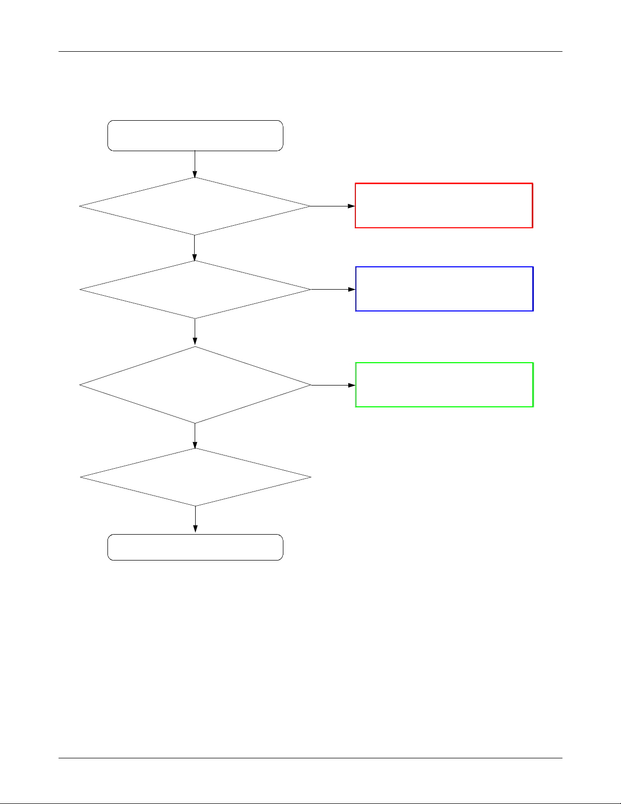
8b-3-1.
Power On
Power On'does not work
'
Check the Battery Voltage
is more than
check current consumption
C518
(
C520>1.8V, C522,>
>=100
Check U503(PMIC) and
Power on voltage
V, C519
>1.2
>1.8
Yes
Yes
mA
Yes
V)
3.3V
1.2V
>1.1
V,
C529
No
No
No
Check the problem point(short, open, crack etc)
Change the Battery
Because of batt. power low)
(
Download again
and If PMIC has problem, change U503
Yes
Check Resistance Values of
C230, C231, C518, C554. Are
the values are less than
check the initial operation
ohm?
No
Check the Clock at
OSC501 that
Frequency is
Yes
Yes
END
100
32K
Yes
No
Replace capacitor or capacitors that has/have less
than
Resolder or Replace OSC501, C517 and
ohm resistance.
100
C539
8-5
SAMSUNG Proprietary-Contents may change without notice
This Document can not be used without Samsung's authorization
Page 53

Level3Repair
8-6
SAMSUNG Proprietary-Contents may change without notice
This Document can not be used without Samsung's authorization
Page 54

Level3Repair
8-7
SAMSUNG Proprietary-Contents may change without notice
This Document can not be used without Samsung's authorization
Page 55

Level3Repair
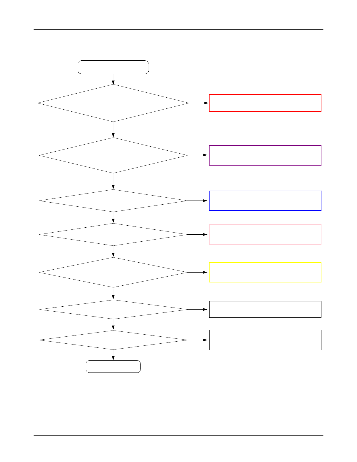
8b-3-2.
Initial
Initial Failure
Yes
The pin
swing properly
The pin
swing properly
AP_PS_HOLD(TP501) and
AP_N_RST_IN(R507)
lowHigh"?
"
There is
32.768
at OSC200 and OSC501
of U206
#1,2
1.8V
of U206=
#11,12
2.8V
Yes
Yes
KHz wave forms
Yes
=
and0V?
and0V?
=
No
check U206 and UCP400 and related parts(short,
No
if U503 has some problem, it is to be replaced)
(
No
Check U503(crack, open, etc)
Replace OSC
crack, etc)
200
and OSC501
R233
There are24MHz wave forms at
OSC400 and26MHz wave forms
at OSC100(C128)
LCD display OK?
Sound is OK?
>= 1.8
END
V?
Yes
Yes
Yes
Yes
No
No
No
No
Check UCP200 and related parts(short, crack,
Replace OSC
Check the LCD part(short, crack, etc)
Check the Audio Part(short, crack, etc)
etc)
and OSC100
400
8-8
SAMSUNG Proprietary-Contents may change without notice
This Document can not be used without Samsung's authorization
Page 56

Level3Repair
8-9
SAMSUNG Proprietary-Contents may change without notice
This Document can not be used without Samsung's authorization
Page 57

Level3Repair
8b-3-3.
Charging Part
Check IFC300 pin#1whether
voltage reading is greater than
Check U503 DCIN whether
Abnormal charging part
Yes
4.9V
Yes
is measured
C502)
(
Yes
5V
No
No
Check the TA
TA may not be connected properly)
(
Resolder or Replace U301
Battery is charging?
Yes
END
No
Resolder or Replace U503
8-10
SAMSUNG Proprietary-Contents may change without notice
This Document can not be used without Samsung's authorization
Page 58

Level3Repair
8-11
SAMSUNG Proprietary-Contents may change without notice
This Document can not be used without Samsung's authorization
Page 59

Level3Repair
8b-3-4.
Sim Part
NO SIM
Yes
Check the connection of
the HEA301
Yes
Check the Sub PCB
Yes
END
No
Reconnect the Sub PCB
T_FLASH_D(0)
T_FLASH_D(2)
T_FLASH_DETECT
SPK_OUT_R_P
SPK_OUT_R_N
R330
VTF_2.8V
HEA301
1
3
5
7
9
111112
15
C
C
N
N
8
7
1
1
U
5
C517
C539
1
0
5
P
T
C553
C
3
2
C
9
2
8
C
3
4
3
0
V
3
1
6
2
2
4
4
6
6
8
8
10
10
12
C
C
N
N
0
9
1
2
C
5
1
L502
9
C
5
1
L501
8
R
R
4
4
3
3
5
7
R
R
4
4
2
2
C508
2
4
C
C
C
5
5
5
0
0
5
6
9
4
R
3
U
5
0
5
3
0
SC610
1
3
5
7
9
13 13 14 14
15 1616
C330
V307V306 V310
C329
C
3
3
9
C
5
3
C533
7
R326
R327
C336
C337
C
3
3
3
C338
U
3
0
C340
7
R328
R329
R340
R331
R
6
0
4
L
6
C
0
6
1
0
V311
1
V312
U
6
V310
0
R
C
1
6
2
0
0
1
8
R603
0
3
C532
C536
C
C
C538
C
5
5
3
5
3
4
5
0
C
4
3
3
2
C501
C
C
C503
5
5
OSC501
2
2
2
3
R501
1
0
3
A
V308
E
V307
H
V306
V309
CP_VSIM_1.8VVCC_2.8V_PDA
T_FLASH_D(1)
T_FLASH_D(3)
T_FLASH_CLKT_FLASH_CMD
SIM_RST
SIM_CLK
SIM_IO
AP_JTAG_EXTRST
V311V309
V312V308
R
R
R
4
4
4
3
3
3
4
8
3
R
R
R
4
4
4
2
2
2
5
9
8
C
4
C
1
4
5
1
0
C
4
1
3
C541
R468
R467
C542
V316
8-12
SAMSUNG Proprietary-Contents may change without notice
This Document can not be used without Samsung's authorization
Page 60

Level3Repair
8b-3-5.
Microphone Part
Check main microphone function
in voice call receiver mode
Yes
Check Sub-Touch Module
FPCB where main Mic is
placed for any damage(Tear
Yes
Check the voltage at C267
2.8V
No
=
No
Change the Sub-Touch Module
Resolder or replace U210
Yes
Check component soldering
statuses of C281, C282
Yes
END
No
Resolder or replace C281, C282
8-13
SAMSUNG Proprietary-Contents may change without notice
This Document can not be used without Samsung's authorization
Page 61

Level3Repair
8-14
SAMSUNG Proprietary-Contents may change without notice
This Document can not be used without Samsung's authorization
Page 62

Level3Repair
8b-3-6.
Speaker Part
Play MP3 with maximum volume level.
Check speaker function.
Yes
Check the connection of
HEA301
Yes
Check signals on L209,
L210
Yes
No
No
Reconnect HEA301
Resolder or replace U207
Replace the speaker
module
Yes
END
Yes
Check signals on
L209, L210 again
No
Replace UCP400
8-15
SAMSUNG Proprietary-Contents may change without notice
This Document can not be used without Samsung's authorization
Page 63

Level3Repair
8-16
SAMSUNG Proprietary-Contents may change without notice
This Document can not be used without Samsung's authorization
Page 64

Level3Repair
8b-3-7.
Receiver Part
Check receiver function in voice call receiver
mode
Yes
Check the signals at ZD307,
Check the signals at ZD307,
Check the connection of
ZD308
Yes
ZD308 again
Yes
HDC302
No
No
No
Resolder or replace U207
Resolder or replace UCP200
Reconnect HDC302
Yes
Replace the Receiver-Earjack
Ass'y
Yes
END
8-17
SAMSUNG Proprietary-Contents may change without notice
This Document can not be used without Samsung's authorization
Page 65

Level3Repair
8-18
SAMSUNG Proprietary-Contents may change without notice
This Document can not be used without Samsung's authorization
Page 66

Level3Repair
8b-3-8.
BT/WIFI
Check the Voltage on C162
BT/WiFi is not working
Check BT or WiFi function
Check
ON
Yes
2.8V
Yes
MHz Clock at
38.4
C177
Yes
No
=
No
No
etc.(If U503 has some problem, it needs to
Enable BT or WiFi Function
Check AP PMIC(U503) for Crack, Open or
be replaced)
Check OSC
102
heck the Voltage on L113
C
Check the Status of C138,
Resolder or Replace U105
1.2V
Yes
L124, ANT106
Yes
Yes
END
=
No
No
Resolder or change L113
Resolder or Replace C138, L124, ANT106
8-19
SAMSUNG Proprietary-Contents may change without notice
This Document can not be used without Samsung's authorization
Page 67

Level3Repair
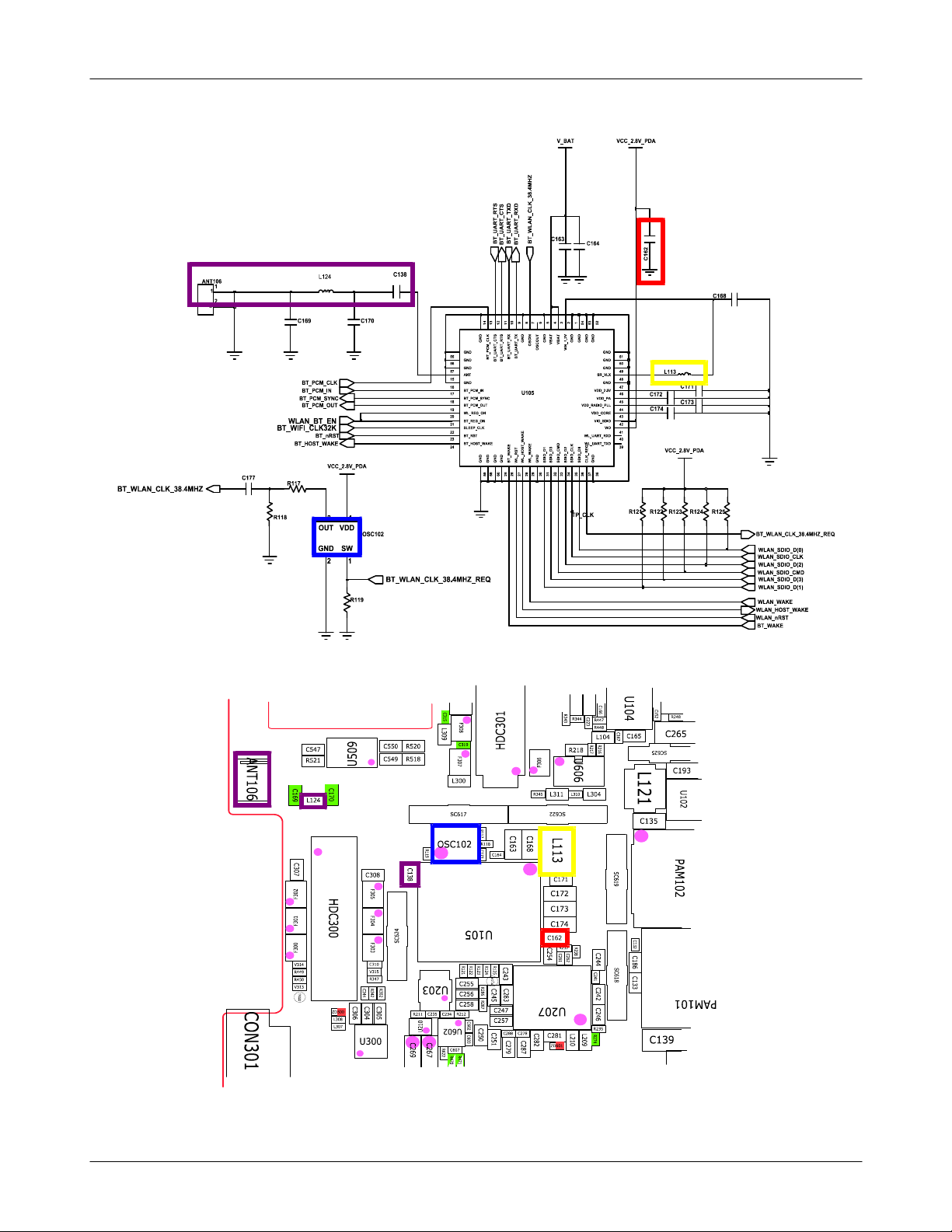
BT_WLAN_CLK_38.4MHZ
ANT702
2
V_BAT VCC_2.8V_PDA
Z
H
M
4
.
8
3
_
K
S
D
D
S
L
T
X
X
T
C
R
T
R
C
_
_
_
_
_
N
T
T
T
T
A
R
R
R
R
L
A
A
A
A
W
U
U
U
U
_
_
_
_
_
T
T
T
T
T
C717
B
B
B
B
B
1
1
2
L703
C721
BT_PCM_CLK
BT_PCM_IN
BT_PCM_SYNC
BT_PCM_OUT
WLAN_BT_EN
BT_WIFI_CLK32K
BT_nRST
BT_HOST_WAKE
R701
VCC_2.8V_PDA
3
OUT
GND
2
VDD
SW
C727
R702
C719
4
0
1
3
GND
GND
GND
ANT
GND
BT_PCM_IN
BT_PCM_SYNC
BT_PCM_OUT
WL_REG_ON
BT_REG_ON
SLEEP_CLK
BT_RST
BT_HOST_WAKE
2
7
8
9
1
1
1
1
1
S
X
S
X
K
D
N
G
N
D
I
T
L
T
T
R
N
C
_
_
C
C
R
G
S
T
_
T
_
_
T
T
O
R
R
M
A
R
R
A
C
A
A
U
U
P
_
_
U
U
_
T
T
_
_
T
B
T
T
B
B
B
B
U702
E
K
A
W
_
E
T
E
K
S
K
T
A
A
O
S
H
R
W
W
D
D
D
D
_
_
_
_
L
L
N
G
L
N
N
N
T
G
G
B
G
W
W
W
8
5
9
0
7
6
8
5
9
2
5
6
2
2
2
2
C722
55
56
57
15
16
17
18
19
20
21
22
23
24
4
OSC701
1
BT_WLAN_CLK_38.4MHZ_REQ
R708
C718
6
1
7
C
C720
4
2
3
3
5
1
2
4
6
5
5
T
U
O
C
S
O
D
N
G
5
V
T
T
D
D
D
D
N
G
1
D
_
O
I
D
S
0
3
D
2
A
A
.
N
N
N
N
1
B
B
G
G
G
G
_
V
V
N
I
V
GND
51
GND
50
GND
49
SR_VLX
GND
VDD_2.5V
VDD_PA
VDD_RADIO_PLL
VDD_CORE
VIO_SDIO
VIO
WL_UART_RXD
D
WL_UART_TXD
K
Q
3
M
2
L
0
E
D
C
D
C
D
R
_
_
_
_
_
_
O
O
O
O
O
D
I
I
I
I
I
K
N
L
D
D
D
D
D
S
S
S
S
S
C
G
1
2
3
4
7
5
8
6
3
3
3
3
3
3
3
3
TP_CLK
L704
48
47
46
45
44
43
42
41
40
39
C724
C726
C723
C725
VCC_2.8V_PDA
R707R705 R706R704R703
BT_WLAN_CLK_38.4MHZ_REQ
WLAN_SDIO_D(0)
WLAN_SDIO_CLK
WLAN_SDIO_D(2)
WLAN_SDIO_CMD
WLAN_SDIO_D(3)
WLAN_SDIO_D(1)
WLAN_WAKE
WLAN_HOST_WAKE
WLAN_nRST
BT_WAKE
8-20
SAMSUNG Proprietary-Contents may change without notice
This Document can not be used without Samsung's authorization
Page 68

Level3Repair
8b-3-9.
FM RADIO
Check the Audio Signal at
Check the Audio signal at
FM Radio does not work
Yes
Check the connection of
HDC302
Yes
L302, L303
Yes
C250, C251
No
No
No
Connect Earjack Ass'y correctly to HDC302
Check Earphone
Check Audio Codec IC(U207)
Yes
Change U700
Yes
END
8-21
SAMSUNG Proprietary-Contents may change without notice
This Document can not be used without Samsung's authorization
Page 69

Level3Repair
C709
FM_EAR_ANT
FM_RST
FM_SCL_2.8V
FM_SDA_2.8V
FM_INT
VCC_2.8V_PDA
R700
C705
8
7
4
3
5
6
9
1
1
1
1
1
1
1
C
O
C
D
C
LOUT
A
N
P
N
N
N
V
1
NC
2
FMI
3
RFGND
4
_RST
12
G
G
ROUT
11
U700
GND
10
VD
9
RCLK
K
O
N
I
L
O
E
D
I
C
S
S
V
S
_
7
5
6
8
L702
RADIO_L
RADIO_R
FM_CLK32K
C711
C710
C712
8-22
SAMSUNG Proprietary-Contents may change without notice
This Document can not be used without Samsung's authorization
Page 70

Level3Repair
8b-3-10.
LCD
LCD is still off after PWR ON
Check the connection of
Check the soldering status of
Check VCC_3.0V_LCD
3.0V (
1.8V (
HDC300
EMI Filters F300~F305
C537), VLCD_1.8V
C307), V_BAT
C308)
(
Yes
Yes
Yes
=
=
>3.4V
No
No
No
Reconnect the HDC300
Resolder EMI Filters
Check PMIC(U503)
Yes
Replace LCD Module
Yes
END
8-23
SAMSUNG Proprietary-Contents may change without notice
This Document can not be used without Samsung's authorization
Page 71

Level3Repair
8-24
SAMSUNG Proprietary-Contents may change without notice
This Document can not be used without Samsung's authorization
Page 72

Level3Repair
8b-3-11.
TSP
Touch Screen does not work
Yes
Check LCD Connector on
Main PBA
Yes
Check the TSP Connector on
LCD Module
U300 Pin
C310) and Pin
6=2.8V(
C306, C344)
(
Yes
C305,
8=3.3V
No
No
No
Reconnect the HDC300
Reconnect TSP Connector
Resolder or Replace U300
Yes
Replace LCD Module
Yes
END
8-25
SAMSUNG Proprietary-Contents may change without notice
This Document can not be used without Samsung's authorization
Page 73

Level3Repair
8-26
SAMSUNG Proprietary-Contents may change without notice
This Document can not be used without Samsung's authorization
Page 74

Level3Repair
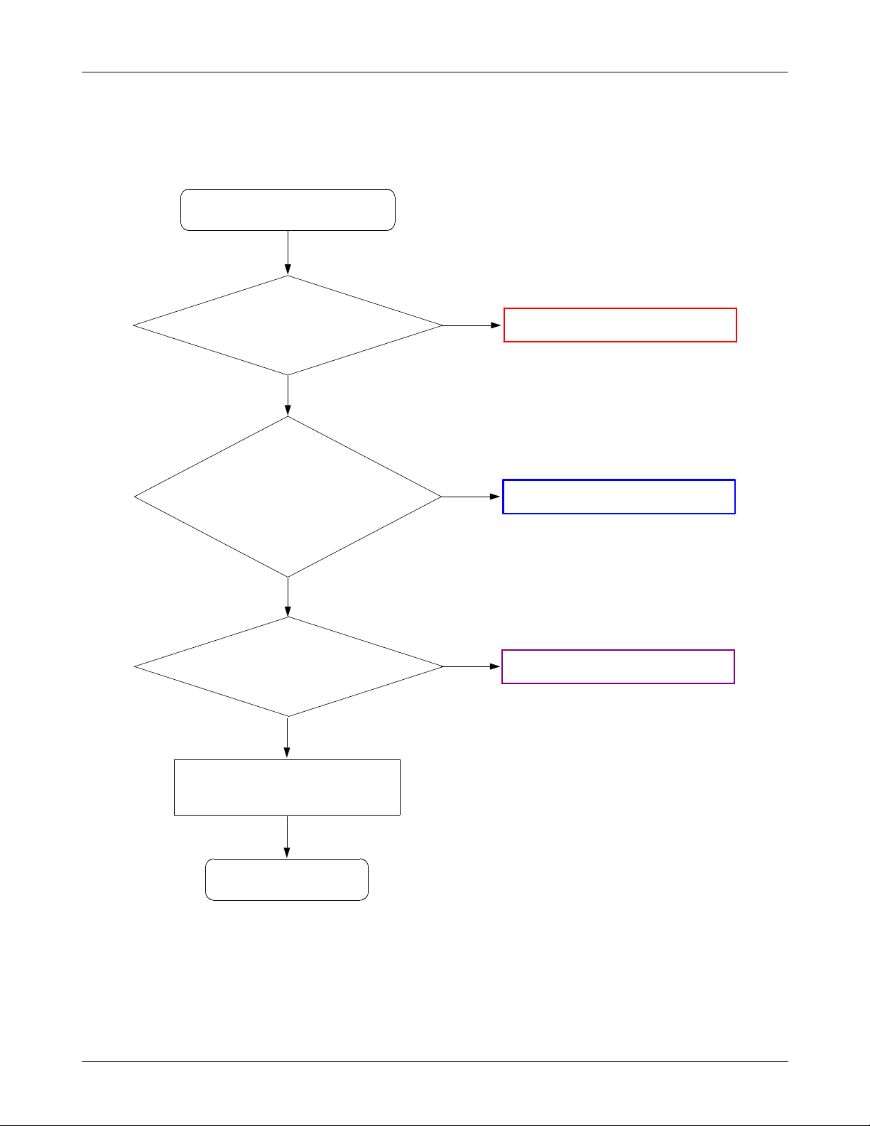
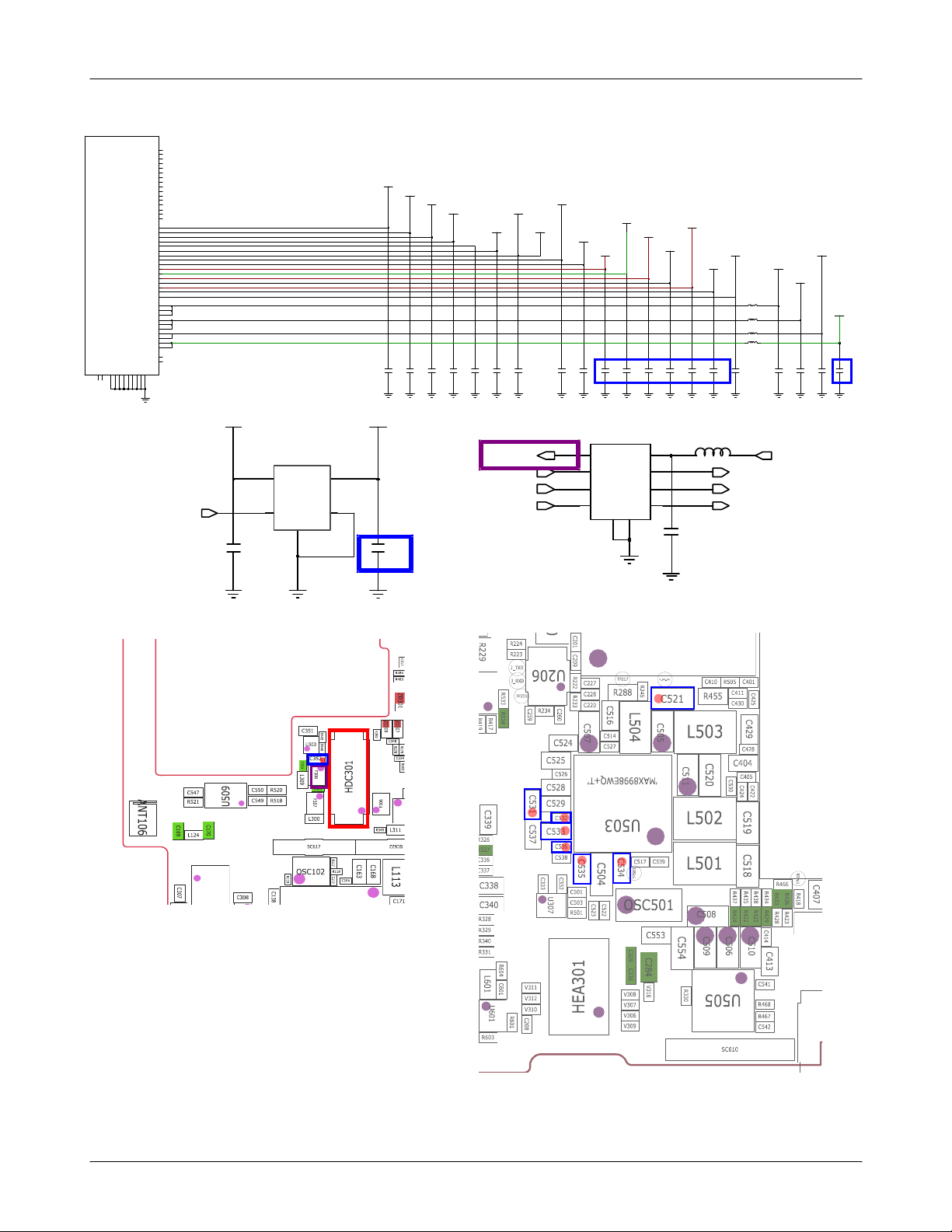
8b-3-12. 5M
CAM
Camera" function does not work
"
Yes
Check the Camera
connector on Main PBA
Yes
Check the voltage
C531,C533,C535
C534, C536
C532, C521
C352
=1.8
=1.2V
=2.8V
=2.8
V,
No
V,
No
Reconnect the HDC301
Resolder U503, U303 or change PBA
Yes
Check F308 Pin1is24MHz
Yes
Replace the camera module
END
No
Check UCP400 related to24MHz
8-27
SAMSUNG Proprietary-Contents may change without notice
This Document can not be used without Samsung's authorization
Page 75

Level3Repair
T
T
T
L
N
N
N
N
G
I
I
I
T
T
V
A
O
H
C
C
O
A
A
B
C
M
D
D
C
I
B
B
T
T
V
V
E
T
D
A1
A
B
BUCK1
IN1
A2
IN1
E1
IN2
BUCK2
E2
IN2
H1
IN3
BUCK3
H2
IN3
K2
IN4
BUCK4
K8
LDO4,5,7
IN5
K9
IN5
C9
IN6
LDO11,12,13
D9
IN6
A7
IN7
LDO14,15,16
B7
IN7
G9
LDO6,8,9
IN8
H9
IN8
B9
IN9
LDO2,3,10,17
B8
LDO2
C8
LDO3
K10
LDO4
U503
4
D
N
C
C
G
N
N
P
4
1
2
K
J10
LDO5
H10
LDO6
K7
LDO7
G10
LDO8
F10
LDO9
C7
LDO10
E10
LDO11
D10
LDO12
C10
LDO13
A6
LDO14
A8
LDO15
A10
LDO16
B10
LDO17
B1
LX1
B2
LX1
C1
LX1
F1
LX2
F2
LX2
F3
LX2
J1
LX3
J2
LX3
J3
LX4
K3
LX4
A4
XIN
A3
XOUT
3
4
2
2
1
1
2
1
D
D
D
D
D
D
D
D
N
N
N
N
N
N
N
N
G
G
G
G
G
G
G
G
P
A
P
P
P
P
P
A
2
5
1
2
1
5
1
4
J
D
A
D
B
K
G
G
VALIVE_1.2V_C110
0.8V~1.3V UP TO 10mA
VUSB_1.1V_C110
VADC_3.3V_C110
VTF_2.8V
0.8V~1.3V UP TO 50mA
1.6V~3.6V UP TO 300mA
1.6V~3.6V UP TO 300mA
C524 C535
C522
1.6V~3.6V UP TO 150mA
C525
1.6V~3.6V UP TO 150mA
C526
VLCD_1.8V
3.0V~3.6V UP TO 150mA
VUSB_3.3V_C110
VDAC_3.3V_C110
C527 C528
VCC_2.8V_PDA
VPLL_1.2V_C110
C529
CAM_SENSOR_CORE_1.2V
CAM_AF_2.8V
CAM_ISP_SYS_2.8V
CAM_ISP_RAM_1.8V
C532
C533
CAM_ISP_HOST_2.8V
CAM_SENSOR_IO_1.8V
C534
VCC_3.0V_LCD
C536
L502
L503
L504
C537
VARM_1.2V_C110
VINT_1.1V_C110
C518
VCC_1.8V_PDA
CAM_ISP_CORE_1.2V
C519
C521
C520
CAM_IO_EN
V_BAT
C351
U303
VDD4VOUT
3
CE
CAM_SENSOR_A2.8V
CAM_MCLK_F
1
CAM_HSYNC_F
CAM_VSYNC_F
2
GND
D
N
G
5
CAM_PCLK
F308
OUT1
OUT2
OUT3
OUT4
GND
5
6
7
8
1
IN1
2
IN2
3
IN3
4
IN4
GND
C315
L309
CAM_MCLK
CAM_HSYNC
CAM_VSYNC
CAM_PCLK_F
910
C352
8-28
SAMSUNG Proprietary-Contents may change without notice
This Document can not be used without Samsung's authorization
Page 76

Level3Repair
8b-3-13.
GSM
RX
850
NORMAL CONDITION
catch the channel?
NO
Check C104
Check the Voltage at
C134, C131=VBAT
Check C111
Check L100
Check the component
U105,OSC100 soldering
OK?
】
?
YES
】
YES
-65
】
YES
YES
-65
-65
dBm
dBm
dBm
NO
NO
?
?
NO
NO
NO
CHECK soldered
RFS100, L115, C104
resolder or change
U102, C134, C131
resolder or change
C111, U102
resolder or change
F100, C103,C107, L100
resolder or change
U105, OSC100
YES
Check C188
Check the voltage at
C125=V_BAT
{
2.85V ?}& {
V?}&{C188
1.8
Check the freq. at C185
GSM1800 Receiver is
C159, C160
MHz
:26
O.K?
END
=2.8V?
YES
?}& {
YES
YES
YES
C158
= 2.8?}
?
NO
=
=
NO
NO
NO
resolder or change
U101, U108
resolder or change
U105
change or resolder
OSC100
resolder or change
UCP200
8-29
SAMSUNG Proprietary-Contents may change without notice
This Document can not be used without Samsung's authorization
Page 77

Level3Repair
8-30
SAMSUNG Proprietary-Contents may change without notice
This Document can not be used without Samsung's authorization
Page 78

Level3Repair
8b-3-14.
GSM
1800
RX
NORMAL CONDITION
catch the channel?
NO
Check C104
Check the Voltage at
C134, C131=VBAT
Check C135
Check C132
Check the component
U105,OSC100 soldering
OK?
】
?
YES
】
YES
】
YES
YES
-65
-65
-65
dBm
dBm
dBm
NO
NO
?
?
NO
NO
NO
CHECK soldered
RFS100, L115, C104
resolder or change
U102, C134, C131
resolder or change
C135, U102
resolder or change
F102, C133,C136, C132
resolder or change
U105, OSC100
YES
Check C188
Check the voltage at
C125=V_BAT
{
2.85V ?}& {
V?}&{C188
1.8
Check the freq. at C185
GSM1800 Receiver is
C159, C160
MHz
:26
O.K?
END
= 2.82.8V ?
YES
?}& {
= 2.82.8?}
YES
YES
YES
NO
C158
=
=
?
NO
NO
NO
resolder or change
U101, U108
resolder or change
U105
change or resolder
OSC100
resolder or change
UCP200
8-31
SAMSUNG Proprietary-Contents may change without notice
This Document can not be used without Samsung's authorization
Page 79

Level3Repair
8-32
SAMSUNG Proprietary-Contents may change without notice
This Document can not be used without Samsung's authorization
Page 80

Level3Repair
8b-3-15.
WCDMA2100 RX
NORMAL CONDITION
catch the channel?
Check C104
Check the Voltage at
C134, C131=VBAT
Check L107
Check C106
Check F101 Pin
?
】
dBm
-65
YES
Check L105
dBm
-65
YES
】
YES
NO
】
YES
YES
?
-65
?
-65
-65
#1
dBm
dBm
dBm
NO
NO
?
?
NO
NO
NO
NO
CHECK soldered
RFS100, L115, C104
resolder or change
U102, C134, C131
resolder or change
U102, L107, C163
resolder or change
F106, C105,C106, C108, C109
resolder or change
U100, R100
resolder or change
F101, C120, C121, L105
YES
Check C188
Check the voltage at
C125=V_BAT
{
2.85V ?}& {
V?}&{C188
1.8
Check the freq. at C185
WCDMA2100 Receiver is
C159, C160
MHz
:26
O.K?
END
=2.8V?
YES
?}& {
= 2.8?}
YES
?
YES
YES
C158
NO
=
=
NO
NO
NO
resolder or change
U101, U108
resolder or change
U105
change or resolder
OSC100
resolder or change
UCP200
8-33
SAMSUNG Proprietary-Contents may change without notice
This Document can not be used without Samsung's authorization
Page 81

Level3Repair
8-34
SAMSUNG Proprietary-Contents may change without notice
This Document can not be used without Samsung's authorization
Page 82

Level3Repair
8b-3-16.
WCDMA900/GSM900 RX
NORMAL CONDITION
catch the channel?
NO
Check C104
Check the Voltage at
C134, C131=VBAT
Check L107
Check C106
Check F101 Pin
dBm
-65
Check L105
dBm
-65
?
】
YES
】
YES
】
YES
YES
YES
-65
?
?
-65
-65
#1
dBm
dBm
dBm
?
?
NO
NO
NO
NO
NO
NO
CHECK soldered
RFS100, L115, C104
resolder or change
U102, C134, C131
resolder or change
U102, L107, C163
resolder or change
F107, C105, C106, C108, C109
resolder or change
U100, R100
resolder or change
F100, C120, C121, L105
YES
Check C188
Check the voltage at
C125=V_BAT
{
2.85V ?}& {
V?}&{C188
1.8
Check the freq. at C185
WCDMA2100 Receiver is
C159, C160
MHz
:26
O.K?
END
=2.8V?
YES
?}& {
= 2.8?}
YES
?
YES
YES
C158
NO
=
=
NO
NO
NO
resolder or change
U101, U108
resolder or change
U105
change or resolder
OSC100
resolder or change
UCP200
8-35
SAMSUNG Proprietary-Contents may change without notice
This Document can not be used without Samsung's authorization
Page 83

Level3Repair
8-36
SAMSUNG Proprietary-Contents may change without notice
This Document can not be used without Samsung's authorization
Page 84

Level3Repair
8b-3-17.
WCDMA1900/PCS1900 RX
NORMAL CONDITION
catch the channel?
NO
Check C104
Check the Voltage at
C134, C131=VBAT
Check C143
Check C102
Check F102 Pin
dBm
-65
Check C138
dBm
-65
?
】
YES
】
YES
】
YES
YES
YES
-65
?
?
-65
-65
#4
dBm
dBm
dBm
?
?
NO
NO
NO
NO
NO
NO
CHECK soldered
RFS100, L115, C104
resolder or change
U102, C134, C131
resolder or change
U102, C143, C140, L110, C187
resolder or change
F104, C100, C101, C102
resolder or change
U100, R100
resolder or change
F102, C137, C138, C139
YES
Check C188
Check the voltage at
C125=V_BAT
{
2.85V ?}& {
1.8
Check the freq. at C185
WCDMA2100 Receiver is
=2.8V?
C159, C160
V?}&{C188
MHz
:26
YES
O.K?
YES
END
YES
?}& {
= 2.8?}
YES
?
C158
NO
=
=
NO
NO
NO
resolder or change
U101, U108
resolder or change
U105
change or resolder
OSC100
resolder or change
UCP200
8-37
SAMSUNG Proprietary-Contents may change without notice
This Document can not be used without Samsung's authorization
Page 85

Level3Repair
8-38
SAMSUNG Proprietary-Contents may change without notice
This Document can not be used without Samsung's authorization
Page 86

Level3Repair
8b-3-18.
GSM850/900 TX
Check the Tx Power at
C183
】
Check the Tx Power at
U102 PIN#1
Check the Voltage at
C134, C131=VBAT
Check C127 waveform,
Looks like rectangular
Check the voltage C188
U102 PIN
2.8
Check the Tx Power at
#14】4
33
V?
】
YES
NO
YES
YES
YES
dBm
33
dBm
dBm
IN INPI NEON PHON ETOOL
NONSIGNALING MODE
TX POW ER LEVEL : 5
?
?
?
=
NO
NO
NO
NO
NO
NO
resolder or change
RFS100, C115, C104
resolder or change
U102
resolder or change
U102, C134, C131
resolder or change
C127, U105
resolder or change
U108, U101, R104, R103
resolder or change
U105
GSM850 CH : 190
GSM900 CH : 62
IN SPECTRUM ANALYZER
RBW : 1 00KHz
VBW : 100 KHz
SPAN : 10M Hz
REF LEV. : 10dBm
GSM850 : 836.6Mhz
GSM900 : 902.4Mhz
YES
Check the voltage at
C125=V_BAT?}&{C158
{
V?}&{C159, C160
=2.85
V?}&{C188
1.8
Check the freq. at C185
:26
GSM850/900 TX is O.K?
MHz
END
= 2.8?}
YES
?
YES
YES
=
NO
NO
NO
resolder or change
U105
change or resolder
OSC100
resolder or change
UCP200
8-39
SAMSUNG Proprietary-Contents may change without notice
This Document can not be used without Samsung's authorization
Page 87

Level3Repair
8-40
SAMSUNG Proprietary-Contents may change without notice
This Document can not be used without Samsung's authorization
Page 88

Level3Repair
8b-3-19.
DCS1800/PCS1900 TX
Check the Tx Power at
C183
Check the Tx Power at
U102 PIN#1
Check the Voltage at
C134, C131=VBAT
Check C127 waveform,
Looks like rectangular
Check the voltage C188
Check the Tx Power at
U102 PIN
30
】
】
YES
YES
YES
V?
2.8
YES
#25】4
NO
dBm
30
?
dBm
dBm
IN INPINEON PHONE TOOL
NON SIGNALING MODE
TX POWER LEVEL
NO
?
?
=
NO
NO
NO
NO
NO
resolder or change
RFS100, C115, C104
resolder or change
U102
resolder or change
U102, C134, C131
resolder or change
C127, U105
resolder or change
U108, U101, R104, R103
resolder or change
U105
DCS1800 CH
PCS1900 CH
IN SPECTRAL ANALYZER
RBW
: 100
VBW
: 100
SPAN
:10
REF LEV
DCS1800
PCS1900
: 1747.4
: 1880
KHz
KHz
MHz
:10
: 698
: 661
dBm
MHz
MHz
:0
YES
Check the voltage at
C125=V_BAT
{
C158
{
= 2.85V ?}& {
C160
=1.8
2.8?}
Check the freq. at C185
:26
DCS1800/PCS1900
Receiver is O.K?
V?}&{C188
YES
MHz
?
YES
YES
END
?}&
C159,
NO
=
NO
NO
resolder or change
U105
change or resolder
OSC100
resolder or change
UCP200
8-41
SAMSUNG Proprietary-Contents may change without notice
This Document can not be used without Samsung's authorization
Page 89

Level3Repair
8-42
SAMSUNG Proprietary-Contents may change without notice
This Document can not be used without Samsung's authorization
Page 90

Level3Repair
8b-3-20.
WCDMA2100 TX
Check the Tx Power at
C183
Check the Tx Power at
U102 PIN#1
Check the Voltage at
C134, C131=VBAT
Check the Tx Power at
Check the Tx Power at
Check the Tx Power at
C163
C166
C165
22.5
】
】
23
】
NO
23
】
】
NO
22.5
YES
YES
YES
dBm
4
dBm
dBm?
dBm?
dBm
IN INPINEON PHONE TOOL
NON SIGNALING MODE
?
?
NO
NO
NO
YES
NO
YES
resolder or change
RFS100, C115, C104
resolder or change
U102
resolder or change
U102, C134, C131
resolder or change
U102
resolder or change
F106, L107, C163
resolder or change
F105, U104
TX DAC
W2100 CH
IN SPECTRAL ANALYZER
RBW
VBW
SPAN
REF LEV
W2100
: 860
: 100
: 100
:10
:10
: 1950
: 9750
KHz
KHz
MHz
dBm
MHz
NO
Check the Tx Power at
C165
Check the voltage at
C125=V_BAT
{
C158
{
= 2.85V ?}& {
C160
=1.8
Check the freq. at C185
WCDMA2100
Transmitter is O.K?
】
V?}&{C188
2.8?}
MHz
:26
END
dBm
4
YES
YES
YES
YES
?}&
?
C159,
NO
NO
=
NO
NO
resolder or change
U105
resolder or change
U105, U101, U108
change or resolder
OSC100
resolder or change
UCP200
8-43
SAMSUNG Proprietary-Contents may change without notice
This Document can not be used without Samsung's authorization
Page 91

Level3Repair
8-44
SAMSUNG Proprietary-Contents may change without notice
This Document can not be used without Samsung's authorization
Page 92

Level3Repair
8b-3-21.
WCDMA1900 TX
Check the Tx Power at
C183
Check the Tx Power at
U102 PIN#1
Check the Voltage at
C134, C131=VBAT
Check the Tx Power at
Check the Tx Power at
Check the Tx Power at
C140
C145
C144
22.5
】
】
23
】
NO
23
】
】
NO
22.5
YES
YES
YES
dBm
4
dBm
dBm?
dBm?
dBm
IN INPINEON PHONE TOOL
NON SIGNALING MODE
?
?
NO
NO
NO
YES
NO
YES
resolder or change
RFS100, C115, C104
resolder or change
U102
resolder or change
U102, C134, C131
resolder or change
U102
resolder or change
F104, C143, C130, L110, C187
resolder or change
F103 U103
TX DAC
W1900 CH
IN SPECTRAL ANALYZER
RBW
VBW
SPAN
REF LEV
W1900
: 860
: 100
: 100
:10
:10
: 1880
: 9400
KHz
KHz
MHz
dBm
MHz
NO
Check the Tx Power at
C144
Check the voltage at
C125=V_BAT
{
C158
{
= 2.85V ?}& {
C160
=1.8
Check the freq. at C185
WCDMA1900
Transmitter is O.K?
】
V?}&{C188
2.8?}
MHz
:26
END
dBm
4
YES
YES
YES
YES
?}&
?
C159,
NO
NO
=
NO
NO
resolder or change
U105
resolder or change
U105, U101, U108
change or resolder
OSC100
resolder or change
UCP200
8-45
SAMSUNG Proprietary-Contents may change without notice
This Document can not be used without Samsung's authorization
Page 93

Level3Repair
8-46
SAMSUNG Proprietary-Contents may change without notice
This Document can not be used without Samsung's authorization
Page 94

Level3Repair
8b-3-22.
WCDMA900 TX
Check the Tx Power at
C183
】
Check the Tx Power at
U102 PIN#1
Check the Voltage at
C134, C131=VBAT
Check the Tx Power at
L108
】
Check the Tx Power at
C174
】
Check the Tx Power at
C179
】
22.5
】
23
NO
23
NO
22.5
YES
YES
YES
dBm
4
dBm
dBm?
dBm?
dBm
IN INPINEON PHONE TOOL
NON SIGNALING MODE
?
?
NO
NO
NO
YES
NO
YES
resolder or change
RFS100, C115, C104
resolder or change
U102
resolder or change
U102, C134, C131
resolder or change
U102
resolder or change
F107, C143, L109, L108
resolder or change
F108, U106
TX DAC
W900 CH
IN SPECTRAL ANALYZER
RBW
VBW
SPAN
REF LEV
W2100
: 860
: 2788
: 100
: 100
:10
:10
: 897.6
KHz
KHz
MHz
dBm
MHz
NO
Check the Tx Power at
C179
Check the voltage at
C125=V_BAT
{
C158
{
= 2.85V ?}& {
C160
=1.8
Check the freq. at C185
WCDMA900
Transmitter is O.K?
】
V?}&{C188
2.8?}
MHz
:26
END
dBm
4
YES
YES
YES
YES
?}&
?
C159,
NO
=
NO
NO
NO
resolder or change
U105
resolder or change
U105, U101, U108
change or resolder
OSC100
resolder or change
UCP200
8-47
SAMSUNG Proprietary-Contents may change without notice
This Document can not be used without Samsung's authorization
Page 95

Level3Repair
8-48
SAMSUNG Proprietary-Contents may change without notice
This Document can not be used without Samsung's authorization
Page 96

b-4. Service Schematics
8
NC Point(Top View)
-
NC
:
UCP400
b
bb
b b
!
" b b
# b bb bbb #
$ bbbb bbbbbbbbbbbbbbbbb bbbb $
% b bbb bbbbbbbbbbbbbbbbb bbbb%
& bbbb bbbbbbbbbbbbbbbbb bb bb &
( bbbb bbb b bb b b b b (
) bbbb bbbbb bbbbbbb bbb bbbb )
* b bbb bbb bbbb b bbbb bbbbbbb *
+ b bbb bbb b bbbbbbbb bbb bbbb +
, b bbb bbb bbb bbb bbb bbbb ,
. b bbb bbb bbb bbb bbb bbbb .
0 bbbb bbb bbb bbbbbb bbbb 0
2 b bbbbbb bbbbbbbbb b b b bbbb 2
3 b bbb b bb bbbbb bbbb b bb bb bb 3
4 b bbb bbb bbbbbbbbb bbb bbbb 4
5 bbbb bbb bbb bbbb 5
7 bbbb bbbbbbbbbbbbb bbbb bbbb 7
b bbb bbbbbbbbb b bbbbbb bbbb b
b bbb bbbbbbbbbbbb b b bbb bbb b
! bbb bbb!
" b bb b bbbbbbbbbbbbbbb b b bb"
# b bbbbbb bbbbbbbbbbbbbbbbbbbb#
$ bbbbbbbbb bbbbbbbbbbb bbbbbbb $
% bbbbbbbbbbbbbbbbbbbbbbbbbbb%
b
b b
bbb
b
b
b
b
bbbbbbbbbbbbbbbbbbbbb
b
b b
bbb
b
b
b bbbbbbbb
bbbbbbbb bbbbbbbbb bbb "
b b
b b b
b
b
b
b b b
b
b
b b
b
b
b bb
b
b bbbb
b
bbbb !
Level3Repair
b
b
8-49
SAMSUNG Proprietary-Contents may change without notice
This Document can not be used without Samsung's authorization
Page 97

Level3Repair
NC
:
UCP200
8-50
SAMSUNG Proprietary-Contents may change without notice
This Document can not be used without Samsung's authorization
Page 98

NC
:
UME301
Level3Repair
8-51
SAMSUNG Proprietary-Contents may change without notice
This Document can not be used without Samsung's authorization
 Loading...