Samsung i8320 Service Manual
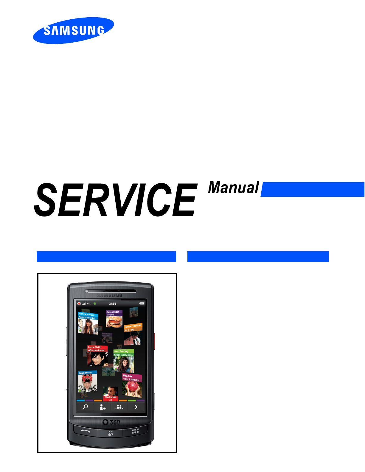
GSM TELEPHONE
GT-i8320
GSM TELEPHONE
CONTENTS
Safety Precautions
1.
Specification
2.
Product Function
3.
Array course control
4.
Exploded View and Parts list
5.
MAIN Electrical Parts List
6.
Block Diagrams
7.
PCB Diagrams
8.
Chart of Troubleshooting
9.
Reference data
10.
Disassembly and Assembly
11.
Instructions

Safety Precautions
1.
Repair Precaution
1-1.
Repair in Shield Box, during detailed tuning. Take specially care of tuning or test, because
―
specipicty of cellular phone is sensitive for surrounding interference(RF noise).
Be careful to useakind of magnetic object or tool, because performance of parts is damaged by
―
the influence of magnetic force.
Surely useastandard screwdriver when you disassemble this product, otherwise screw will be
―
worn away.
Useathicken twisted wire when you measure level.
―
thicken twisted wire has low resistance, therefore error of measurement is few.
A
Repair after separate Test Pack and Set because for short danger(for example an overcurrent
―
and furious flames of parts etc) when you repair board in condition of connecting Test Pack and
tuning on.
Take specially care of soldering, because Land of PCB is small and weak in heat.
―
Surely tune on/off while using AC power plug, becausearepair of battery charger is dangerous
―
when tuning ON/OFF PBA and Connector after disassembling charger.
Don't use as you pleases after change other material than replacement registered on SEC System.
―
Otherwise engineer in charge isn't charged with problem that you don't keep this rules.
1-1
SAMSUNG Proprietary-Contents may change without notice
This Document can not be used without Samsung's authorization

Safety Precautions
ESD(Electrostatically Sensitive Devices) Precaution
1-2.
Several semiconductor may be damaged easily by static electricity. Such parts are called by ESD
Electrostatically Sensitive Devices), for example IC,BGA chip etc. Read Precaution below.
(
You can prevent from ESD damage by static electricity.
Remove static electricity remained your body before you touch semiconductor or parts with
―
semiconductor. There are ways that you touch an earthed place or wear static electricity prevention
string on wrist.
Use earthed soldering steel when you connect or disconnect ESD.
―
Use soldering removing tool to break static electricity.,otherwise ESD will be damaged by static
―
electricity.
Don't unpack until you set up ESD on product. Because most of ESD are packed by box and
―
aluminum plate to have conductive power,they are prevented from static electricity.
You must maintain electric contact between ESD and place due to be set up until ESD is
―
connected completely to the proper place oracircuit board.
1-2
SAMSUNG Proprietary-Contents may change without notice
This Document can not be used without Samsung's authorization

Specification
2.
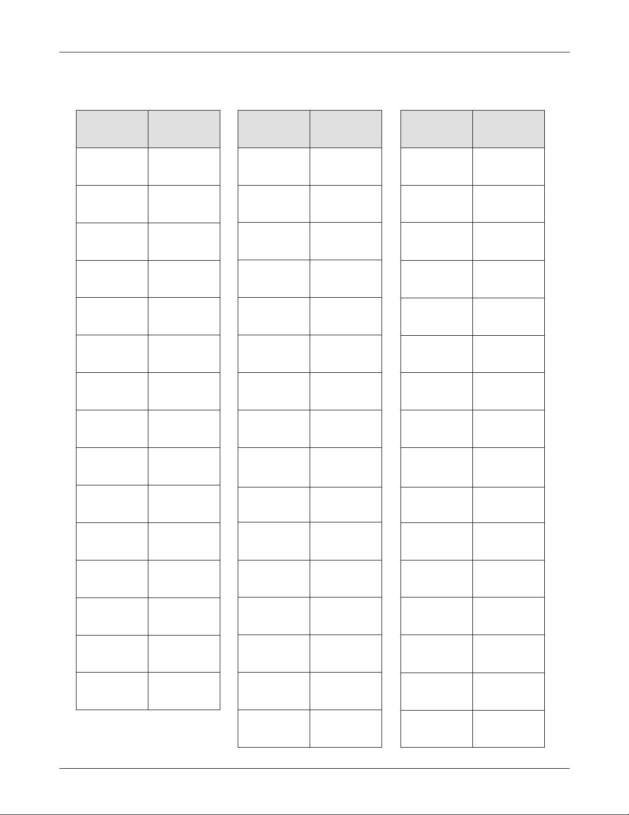
GSM General Specification
2-1.
GSM 850 EGSM 900 DCS 1800 PCS 1900 WCDMA 900 WCDMA 2100
Freq.
Band[MHz]
Uplink/
824~849
869~894
Downlink
880~915
925~960
1710~1785
1805~1880
1850~1910
1930~1990
882.4~912.6
927.4~975.6
1920~1980
2110~2170
ARFCN range
Tx/Rx
spacing
Mod. Bit
rate/
Bit Period
Time Slot
Period/
Frame Period
Modulation
MS Power
128~251
45 MHz 45MHz 90MHz 80MHz 45MH 190MHz
270.833kbps
3.692us
576.9us
4.615ms
0.3GMSK 0.3GMSK 0.3GMSK 0.3GMSK
33dBm~5dBm 33dBm~5dBm 30dBm~0dBm 30dBm~0dBm 24dBm~-50dBm 24dBm~-50dBm
0~124 &
975~1023
270.833kbps
3.692us
576.9us
4.615ms
512~885 512~810
270.833kbps
3.692us
576.9us
4.615ms
270.833kbps
3.692us
576.9us
4.615ms
UL:2712~2863
DL:2937~3088
3.84Mcps
(chip rate)
Frame length :
10ms
Slot length :
0.667ms
QPSK
HPSK
UL:9612~9888
DL:10562~10838
3.84Mcps
(chip rate)
Frame length :
10ms
Slot length :
0.667ms
QPSK
HPSK
Power Class
Sensitivity
TDMA Mux
Cell Radius
4
max
(
dBm)
+33
-102dBm -102dBm -100dBm -100dBm -104.7dBm -106.7dBm
88 8 8 - -
35Km 35Km 2Km 2Km 2Km 2Km
max
(
4
+33
dBm)
max
(
1
+30
dBm)
max
(
1
+30
dBm)
max
(
3
+24
dBm)
max
(
3
+24
dBm)
2-1
SAMSUNG Proprietary-Contents may change without notice
This Document can not be used without Samsung's authorization
Specification
GSM TX power class
2-2.
TX Power
control level
533±2
631±2
729±2
827±2
925±2
10 23±2
11 21±2
GSM850
GSM900
dBm
dBm
dBm
dBm
dBm
dBm
dBm
TX Power
control level
030±3
128±3
226±3
324±3
422±3
520±3
618±3
DCS1800
dBm
dBm
dBm
dBm
dBm
dBm
dBm
TX Power
control level
030±3
128±3
226±3
324±3
422±3
520±3
618±3
PCS1900
dBm
dBm
dBm
dBm
dBm
dBm
dBm
12 19±2
13 17±2
14 15±2
15 13±2
16 11±3
17 9±3
18 7±3
19 5±3
dBm
dBm
dBm
dBm
dBm
dBm
dBm
dBm
716±3
814±3
912±4
10 10±4
11 8±4
12 6±4
13 4±4
14 2±5
dBm
dBm
dBm
dBm
dBm
dBm
dBm
dBm
716±3
814±3
912±4
10 10±4
11 8±4
12 6±4
13 4±4
14 2±5
dBm
dBm
dBm
dBm
dBm
dBm
dBm
dBm
15 0±5
2-2
dBm
15 0±5
SAMSUNG Proprietary-Contents may change without notice
This Document can not be used without Samsung's authorization
dBm

Product Function
3.
Main Function
HSUPA
•
Bluetooth v2.0+EDR
•
Wi-Fi
•
•
•5M
•
•
•
•
•
•
and world time.
•
•
•
•
•
•
•3.5"
(802.11
USB v2.0 HS compatible
CMOS(AF, Power LED)+CIF
Face Detection, Smile Detection, Eye Blink Detection, Panorama Shot, Mosaic Shot
-
FM Radio Receiver
A-GPS, stand alone
DivX Codec
Accelerometer/proximity/ambient light sensor
Instant Messaging capability
Featured applications provide alarms, calendar, calculator, record audio, converter, timer, stopwatch,
File viewer
Multimedia Message Service(MMS)
Multimedia capability(with included Media player)
Speakerphone capability
WEB/WAP browser(HTMS, xHTML, WML)
Movinand16GB+microSD card
AMOLED
Mbps/HSDPA
5.76
b/g)
MBps/Quad(850/900/1800/1900) ,UMTS
7.2
(2100/900)
3-1
SAMSUNG Proprietary-Contents may change without notice
This Document can not be used without Samsung's authorization
Array course control
4.
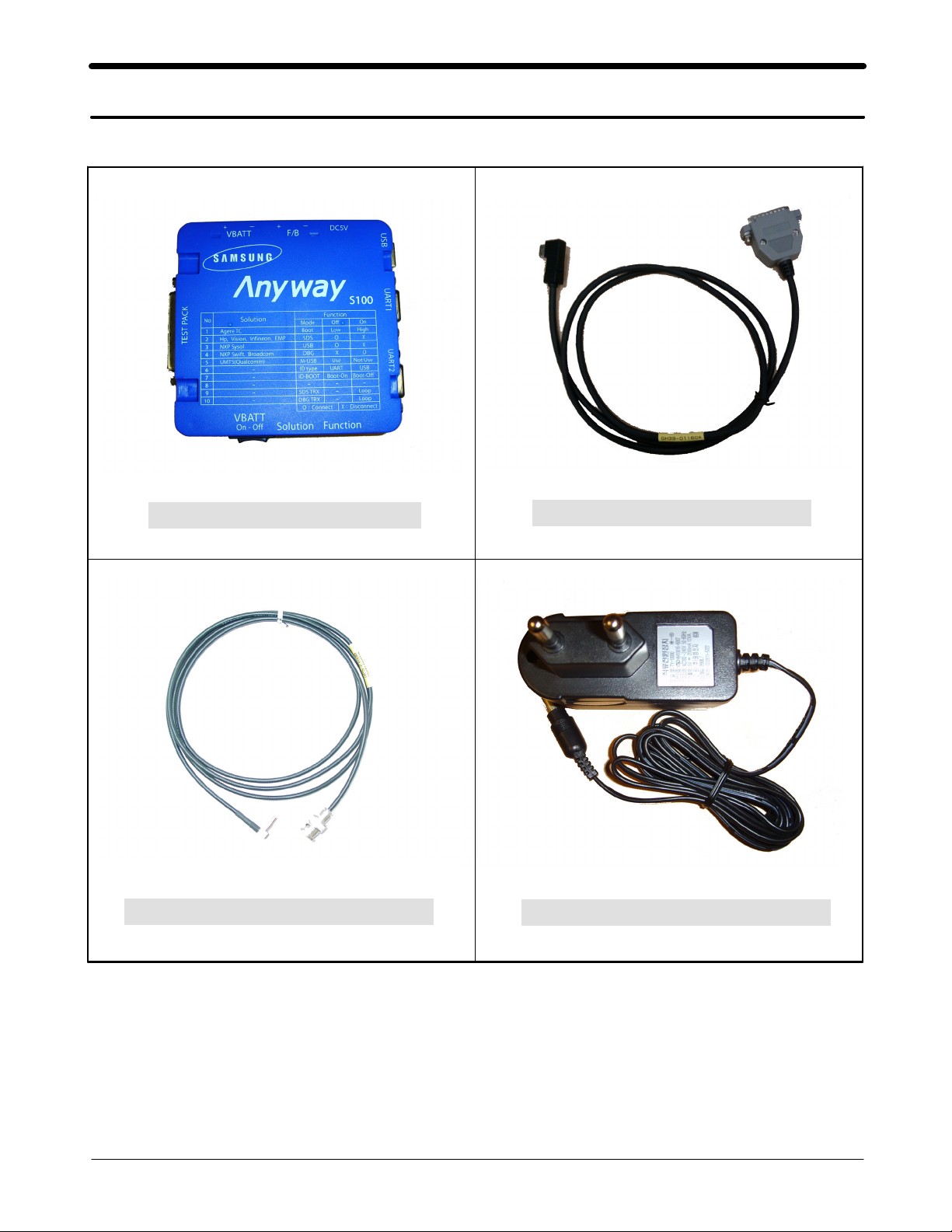
Software Adjustments
4-1.
Test Jig(GH99
RF Test Cable(GH
-36900
39-00985
A)
A)
Test Cable(GH
Adapter(GH
39-01290
99-38251
A)
A)
4-1
SAMSUNG Proprietary-Contents may change without notice
This Document can not be used without Samsung's authorization
Array course control
Software Download
4-2.
4-2-1.
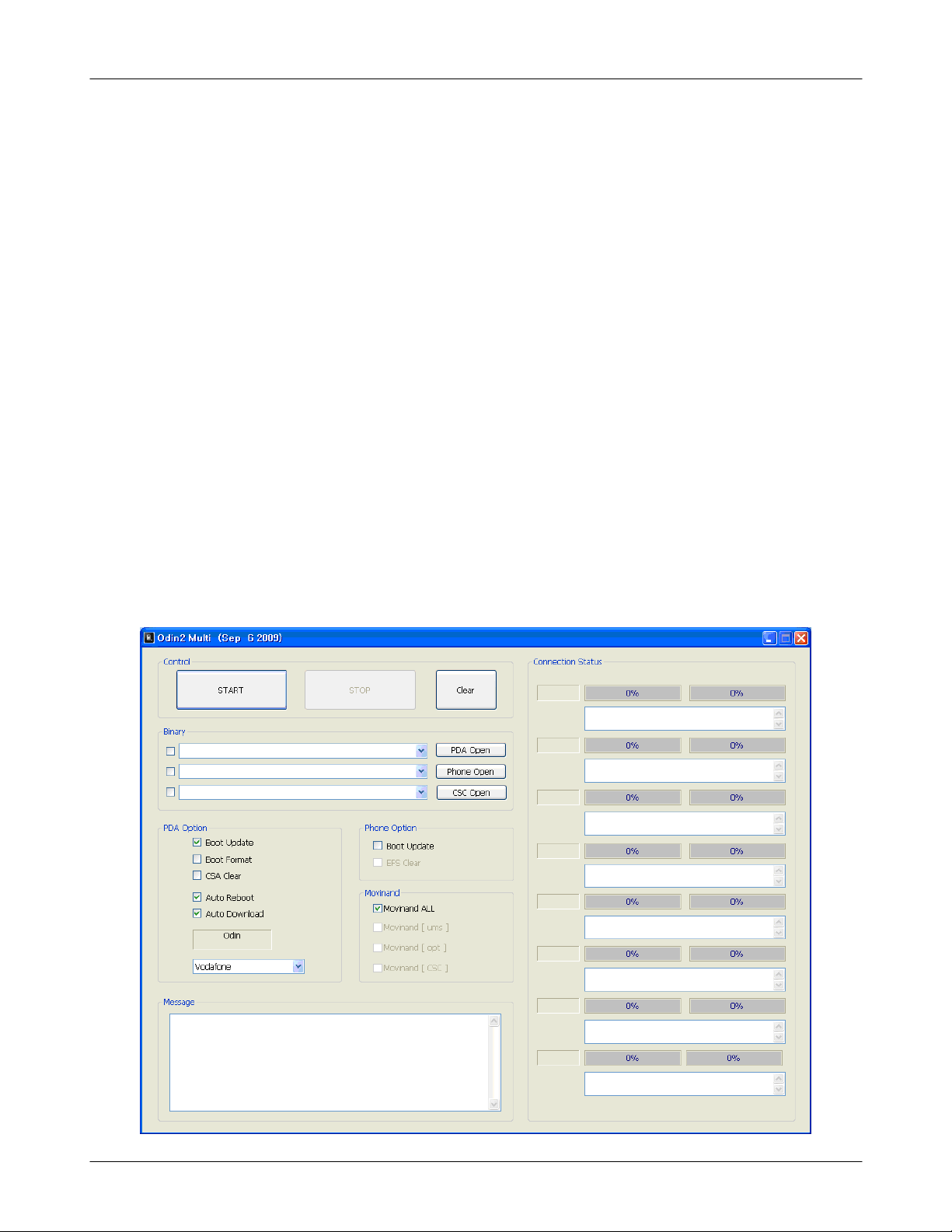
Downloader Program
▶
-
USB Driver
▶
- PDA and Phone:SAMSUNG Mobile USB DRIVER(4.40.7.0) v1.6
GT-i8320(Protector) Target Device
▶
4-2-2.
Make sure that you have installed SAMSUNG Mobile USB Driver in the host PC. If any SAMSUNG
▶
Mobile USB Driver is already installed, the GT-i8320 S/W binary image can be downloaded to the target
device, using the provided USB downloader. But if any error is encountered in installing the SAMSUNG
Mobile USB Driver, you should uninstall the SAMSUNG Mobile USB Driver, re-start the host PC, and fin
ally install again the SAMSUNG Mobile USB Driver.
4-2-3.
Download S/W&USB D river
LComm3Multi_[version].exe
ex. LComm3Multi_090828.exe)
(
Driver Installation(PDA and Phone)
Execute the Downloader Program
[
LComm3Multi_[version].exe
]
4-2
SAMSUNG Proprietary-Contents may change without notice
This Document can not be used without Samsung's authorization
Array course control
4-2-4.
4-2-5.
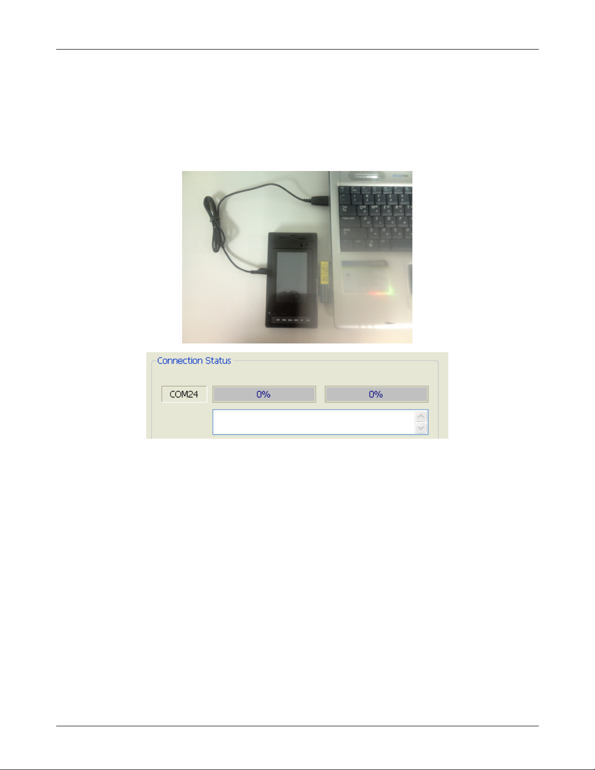
Turn off the device. And then, press the Volume Down key, the Camera key and
the PWR key simultaneously to turn on your device in download mode.(PWR key
should be pressed slightly later than the other keys)
Connect your device to the host PC by using Micro USB DATA Link Cable.
if the device is connected to the host PC successfully, the detected port name, e.g.“COM24”,should
▶
appear as in the above screenshot.
4-2-6.
A. Binaries
(1)
(2)
(3)
B. Binary Download sequence.
-
PDA CSC binary and the Phone binary can also be downloaded at the same time.
-
ce to the target device. The device should be able to operate regardless of the download order of the
inaries.
- However, the PDA CSC binary should be downloaded after the PDA Base binary is downloa
ded.
Download
PDA Base Binary: Base binary to operate the device including PDA bootloader, kernel, platform,
pplication, and all programs for PDA.
PDA CSC Binary: CSC binary including all regional settings for every country.
Phone Binary: Phone modem binary.
The PDA Base binary and the Phone binary can be downloaded simultaneously or separately. The
The order in which the PDA Base binary and the Phone binary are downloaded makes no differen
Otherwise, the regional settings accompanied by the PDA CSC binary have no impact on the targe
SAMSUNG Proprietary-Contents may change without notice
This Document can not be used without Samsung's authorization
4-3
a
b
Array course control
device.
t
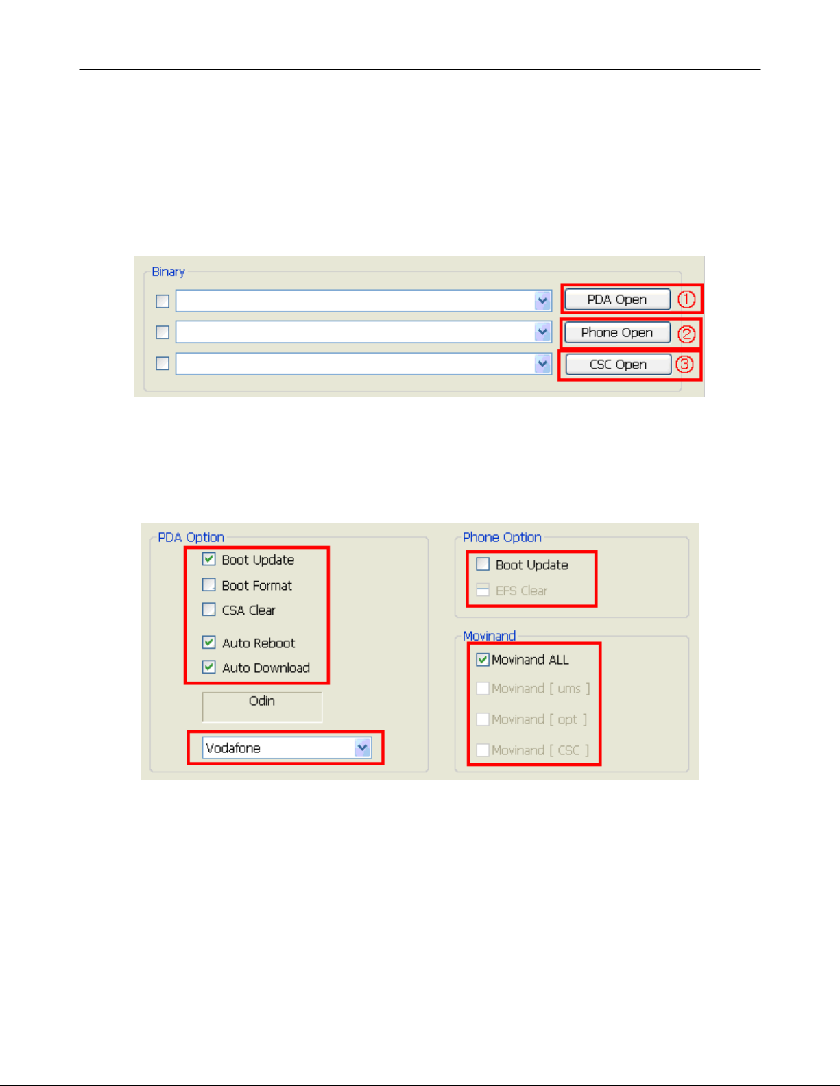
Open Binary File
C.
①
②
③
Open the PDA Base Binary.
Open the Phone Binary.
Open the PDA CSC Binary.
※
It is possible to download each binary one-by-one.
D. Download Options
PDA Option
▶
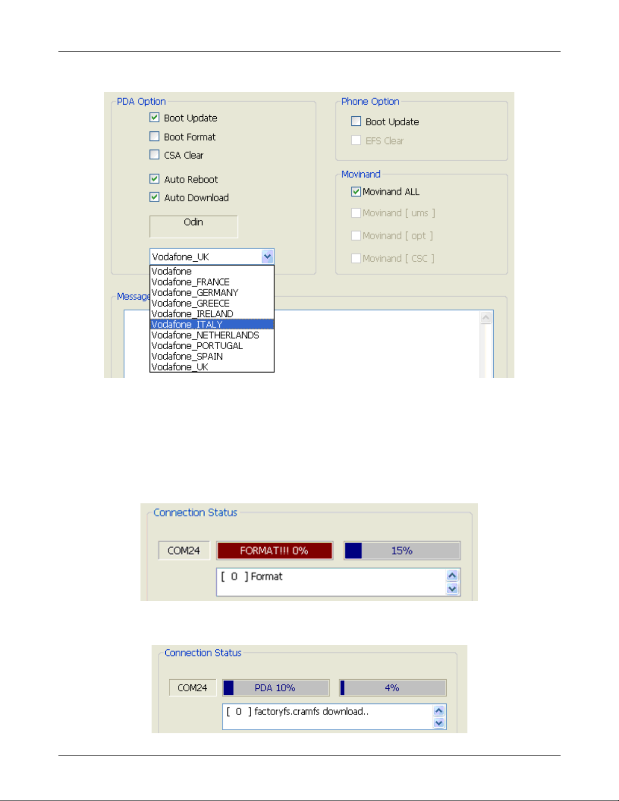
Boot Update: Update the Bootloader. It should be enable when the PDA Base binary is downloaded.
-
Boot Format: Format the partition of the target’sdisk. When there is an explicit notice in the Release
-
Note, Boot Format option should be enabled.
If you don’thave any notice for the PDA Base Binary,
you have to disable Boot Format in PDA Option.
CSA Clear: Option foradeveloper. It should be disabled.
-
Auto Reboot: Automatically reboot the target after download. It should be enabled for stability.
-
Auto Download: When the target connects to the host PC by micro-USB after the Start button is click
-
ed, automatically download the binary. It should be enabled.
4-4
SAMSUNG Proprietary-Contents may change without notice
This Document can not be used without Samsung's authorization

Array course control
Region Select
▶
Chose the country. It is used when the PDA CSC binary is downloaded.
-
Phone Option
▶
-
ote on Phone Boot Update, Boot Update on Phone Option should be enabled.
Boot Update: Update the Modem Bootloader. When there is an explicit notice in the Release
If you don’thave any
otice for the Phone Binary, you have to disable Boot Update in Phone Option.
Movinand
▶
-
Movinand ALL: Option foradeveloper. It should be enabled.
E. Option setting according to the Binaries.
Below table shows the options that should be selected according to the binaries.
▶
Phone
Downloa
Binary
d
Boot
Update
PDA only Enable Disable(2) Disable Enable Enable Don’tCare Disable Enable
Phone only Disable Disable Disable Enable Enable Don’tCare Disable(1) Enable
CSC only Disable Disable Disable Enable Enable Select Disable Enable
PDA, Phone Enable Disable(2) Disable Enable Enable Don’tCare Disable(1) Enable
PDA, CSC Enable Disable(2) Disable Enable Enable Select Disable Enable
Phone, CSC Disable Disable Disable Enable Enable Select Disable(1) Enable
PDA, Phone,
CSC
Enable Disable(2) Disable Enable Enable Select Disable(1) Enable
Boot
Format
PDA Option
CSA
Clear
Auto
Reboot
Auto
Download
Region
Select
Option
Boot
Update
Movinand
Movinand
N
n
ALL
(1), (2)
When there is an explicit notice in the Release Note, those options should be enabled. Be
areful of setting download options. Wrong download setting can damage the device.
F. Download examples
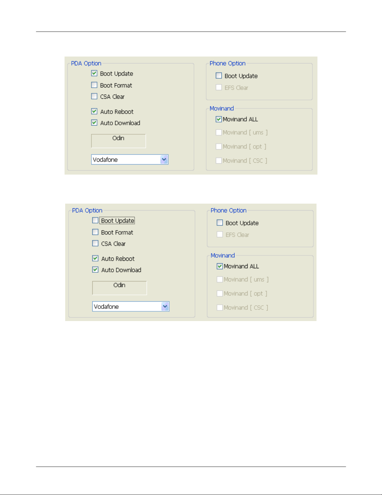
Only the PDA Base Binary is downloaded. Or the PDA Base Binary and the Phone Binary are downl
▶
oaded.
4-5
SAMSUNG Proprietary-Contents may change without notice
This Document can not be used without Samsung's authorization
c
Array course control
Only the Phone binary is downloaded.
▶
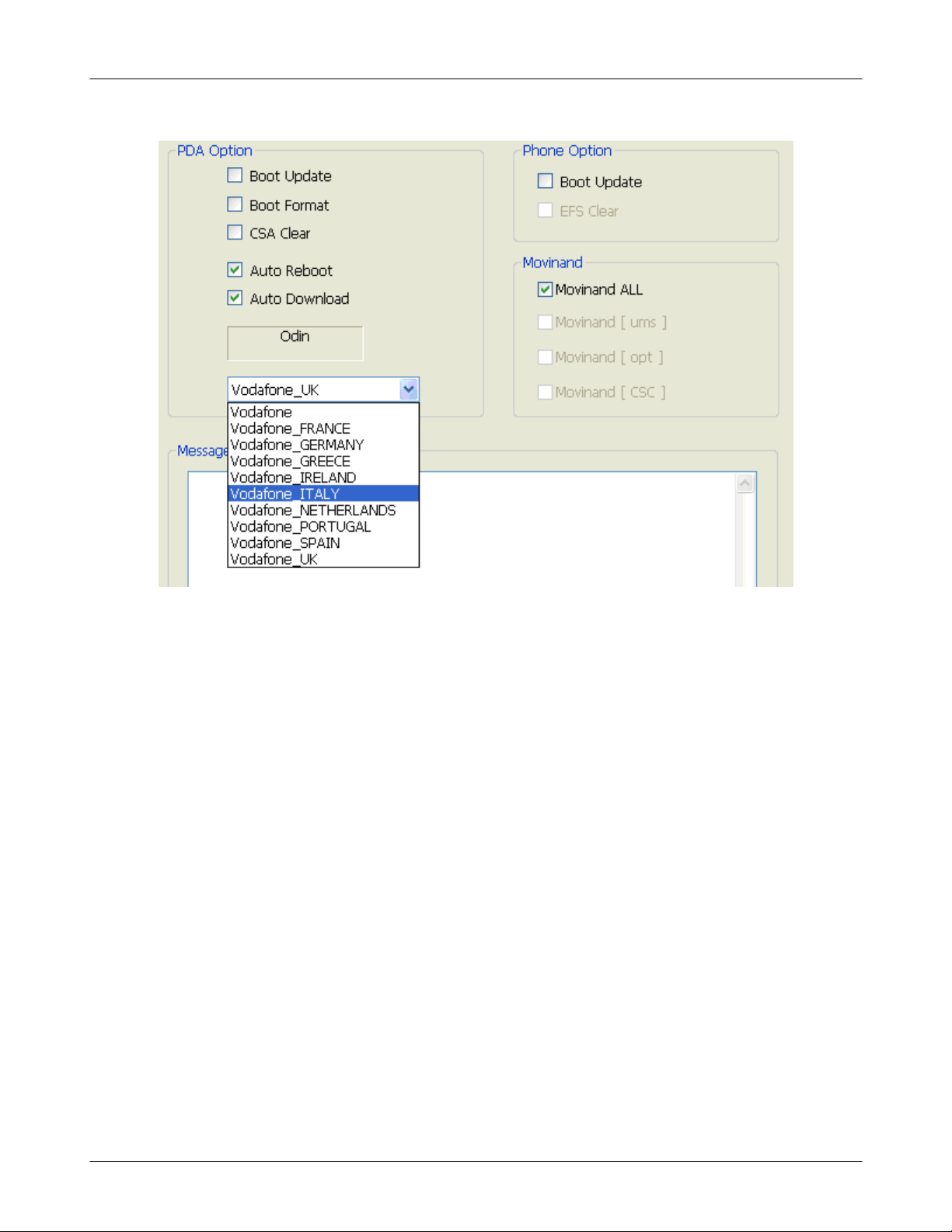
Only the PDA CSC Binary is downloaded. Or the Phone Binary and the PDA CSC Binary are downlo
▶
aded.
-
-
Chose the country.
If you want to change regional setting, only the PDA CSC Binary download is required without the
PDA Base Binary and Phone Binary download.
4-6
SAMSUNG Proprietary-Contents may change without notice
This Document can not be used without Samsung's authorization
Array course control
The PDA Base Binary, the PDA CSC Binary, and the Phone Binary are downloaded. Or the PDA Ba
▶
se Binary and the PDA CSC Binary are downloaded.
4-7
SAMSUNG Proprietary-Contents may change without notice
This Document can not be used without Samsung's authorization
Array course control
Click on the START Button on the downloader program.
G.
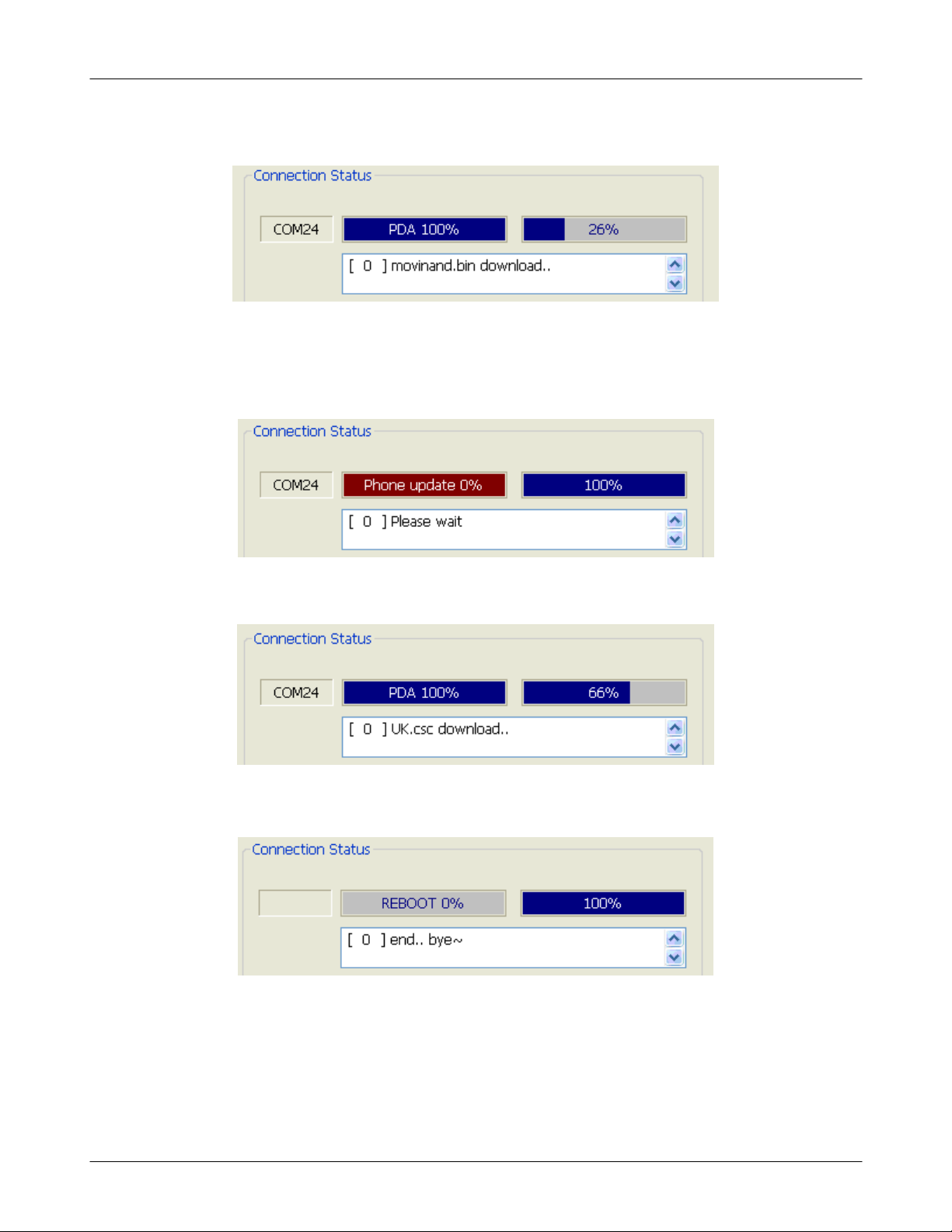
If the Boot Format option is enabled, the downloader formats the partitions.
▶
While the downloader
hows“FORMAT!!”message like above, be careful NOT to turn off the device during the period! If
for any reason the device gets turned off while“FORMAT!!”message shows, the device may get
damaged.
PDA Base Binary download(Screenshot
▶
OneNAND download in progress)
#1:
s
4-8
SAMSUNG Proprietary-Contents may change without notice
This Document can not be used without Samsung's authorization
Array course control
PDA Base Binary download(Screenshot
▶
Phone Binary download.
▶
While the downloader shows“Phone Update”message like above, be
MoviNAND download in progress)
#2:
areful NOT to turn off the device during the period! If for any reason the device gets turned off
while“Phone Update”message shows, the device’smodem may get damaged.
c
PDA CSC Binary download
▶
Download complete.
▶
4-2-7.
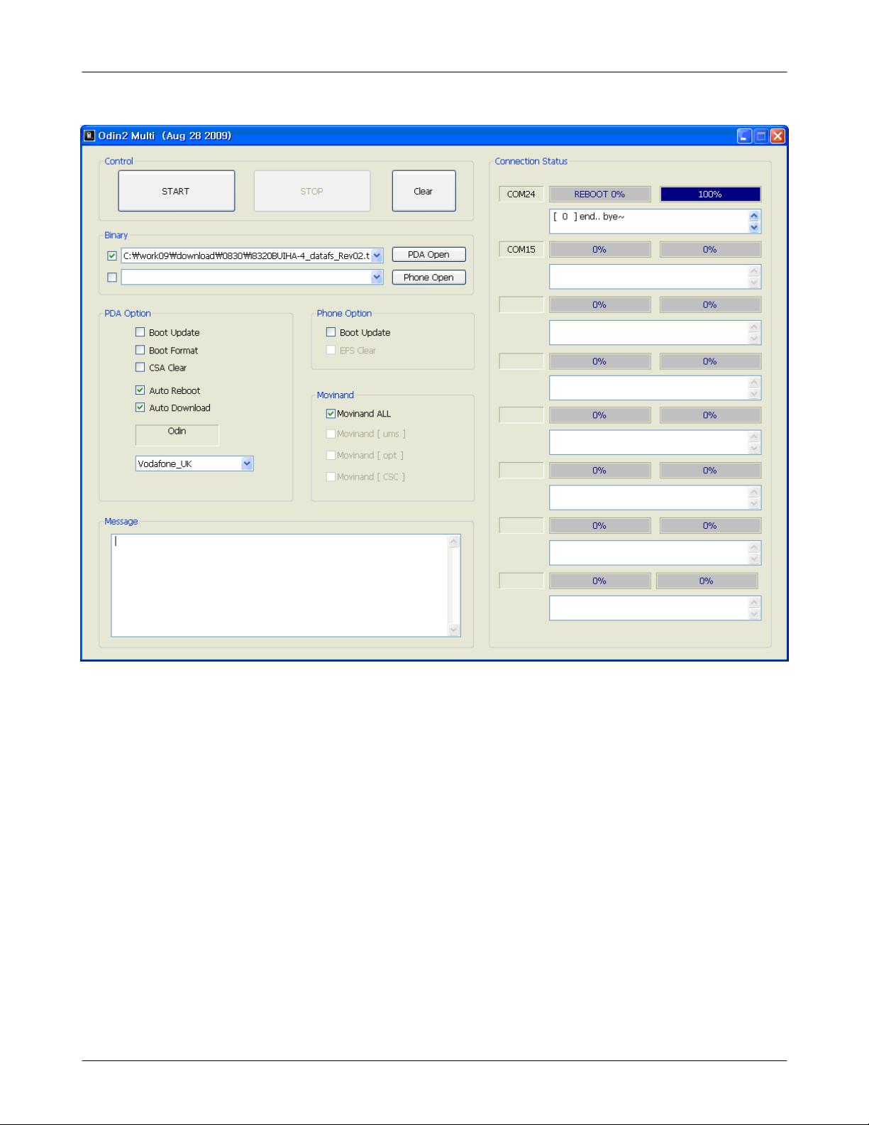
Downloading binaries to multiple devices
Connect multiple devices using USB hub follow the steps
-.
Maximum of8devices can be connected and binaries can be downloaded simultaneously
-.
4-2-4, 4-2-5
4-9
SAMSUNG Proprietary-Contents may change without notice
This Document can not be used without Samsung's authorization
Array course control
4-3.
Trouble Shooting
4-3-1. “
Port Open Failed”message or application hang
4-10
SAMSUNG Proprietary-Contents may change without notice
This Document can not be used without Samsung's authorization

Array course control
After you install“SAMSUNG Mobile USB Driver”,you may see the message“Port open failed
F
…”
or the USB Downloader program hang while downloadingabinary. If so, terminate the Downloade
program and retry the download.
r
If USB port is changed, you may also see the message“Port open failed…”or the USB Downl
F
oader program hang. If so, terminate the Downloader program and retry the download.
If USB cable to the target device is not connected tightly, you may see the message“Port ope
F
failed…”or the USB Downloader hang. If so, terminate the Downloader program and then retry
n
the download.
If you always see“port open failed”message or the USB Downloader program hang,
F
Uninstall the“SAMSUNG Mobile USB DRIVER
1.
Restart your PC.
2.
Install the“SAMSUNG Mobile USB DRIVER
3.
Try the download again.
4.
”
”.
4-3-2. “
F
4-3-3.
F
Write Failed”message
If battery level is low, use charged battery and try again.
Downloading doesn’tstart
If the USB port is not detected&downloading doesn’tstart and displays the following screen,
etry again and when the device is started, keep the PWR key pressed until the USB port is detect
ed&downloading begins.
r
4-11
SAMSUNG Proprietary-Contents may change without notice
This Document can not be used without Samsung's authorization
Exploded View and Parts List
5.
5-1.
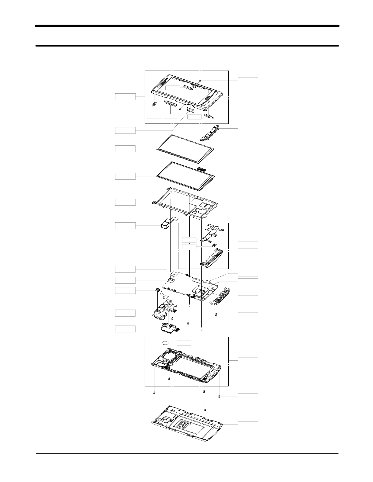
Cellular phone Exploded View
QCK03
QFR01
QVO01
QCK02
QRF06
QME03
QLC01
QLB01
QCA01
QCR03
QCK01
QKP02
QMP01
QMO01
QCA02
QSP01
QSK01
QME01
QMI03
QCW01
QME00
QVK02
QSH01
QAN02
QCR54
QRE01
QCR03
QBC00
5-1
SAMSUNG Proprietary-Contents may change without notice
This Document can not be used without Samsung's authorization
Exploded View and Parts List
5-2.
Cellular phone Parts list
Design LOC Description SEC CODE
QAN02 INTENNA-GT_I8320 MAIN GH42-02219A
QBC00 ASSY COVER-BATT GH98-14338A
QCA01 ASSY CAMERA-GT_I8320
QCA02 ASSY CAMERA-GT_I8320 VGA GH96-04039A
QCR03 SCREW-MACHINE
QCR54 SCREW-MACHINE
QKP02 ASSY KEYPAD-SUB GH98-14340A
QLB01 ASSY BRACKET-LCD GH98-14342A
QLC01 ASSY LCD-3.5" WVGA GT_I8320 AMOLED GH96-04021A
QME03 TOUCH/PANEL-GT_I8320 GH59-08398A
QMO01 MOTOR LINEAR VIBRATION-GTS8000 GH31-00475A
QMP01 A/S ASSY-GT_I8320 PBA MAIN GH82-04168A
QRF06 PMO COVER-USB GH72-55748A
5M
GH96-04077A
6001-001811
6001-001645
QSH01 ASSY COVER-SHILED CAN GH98-14341A
QSK01 MODULE-SIM SOCKET+EARJACK(I8320) GH59-08296A
QSP01 MODULE-GT_I8320 SPK+RCV GH59-08275A
QVK02 KEY FPCB-GT_I8320 CAM KEY GH59-08135A
QME00 ASSY MODULE-GT_I83203DOME+MIC+BRAKET
QME01 KEY FPCB-3 DOME+MIC WHT(GT-I8320) GH59-08032B
QMI03 RMO RUBBER-MIC HOLDER GH73-13284A
QRE01 ASSY CASE-BAR REAR GH98-14337A
QCW01 PCT WINDOW-5G CAM GH72-55758A
QFR01 ASSY CASE-FRONT INTOPS GH98-15337A
QCK02 PMO KEY-POWER GH72-55750A
QCK03 PMO KEY-HOT GH72-55751A
QCK01 PMO KEY-CAMERA GH72-55752A
QVO01 PMO KEY-VOLUME GH72-55817A
W
GH96-04176B
5-2
SAMSUNG Proprietary-Contents may change without notice
This Document can not be used without Samsung's authorization
MAIN Electrical Parts List
6.
SEC code Design Location Discription
0403-001547
0404-001172
0406-001208
0406-001267
0406-001267
0406-001267
0406-001322
0406-001322
0406-001369
0407-001007
0504-001113
0504-001140
0505-001165
0801-002345
0801-003016
0801-003052
0801-003079
0801-003200
0801-003265
0902-002434
1001-001461
1001-001488
1001-001585
1001-001593
1003-002047
1003-002276
1107-001889
1108-000260
1201-002733
1201-002830
1201-002889
1201-002890
1201-002971
1202-001068
1202-001088
1203-004319
1203-004607
D500 DIODE-ZENER
D501,D503,D700,D701 DIODE-SCHOTTKY
ZD900 DIODE-TVS
ZD600,ZD700,ZD701 DIODE-TVS
ZD702,ZD800,ZD801 DIODE-TVS
ZD802,ZD901,ZD902 DIODE-TVS
ZD703,ZD704,ZD803 DIODE-TVS
ZD804,ZD805 DIODE-TVS
D702 DIODE-TVS
D502 DIODE-ARRAY
Q501 TR-DIGITAL
TR700 TR-DIGITAL
Q500 FET-SILICON
U202 IC
U400,U505 IC
U401 IC
U504 IC
U403 IC
U402 IC
UCP1000 IC
U702 IC
U705 IC
U708 IC
U703 IC
U700 IC
U901 IC
UME1000 IC-FLASH MEMORY
UME400 MEMORY
U602 IC
U200 IC
PAM200 IC
PAM201 IC
U300 IC
U802 IC
U709 IC
U701 IC
U704 IC
6-1
SAMSUNG Proprietary-Contents may change without notice
This Document can not be used without Samsung's authorization

Main Electrical Parts List
SEC code Design Location Discription
1203-004819
1203-004857
1203-005298
1203-005434
1203-005516
1203-005690
1203-005722
1203-005772
1203-005783
1204-003026
1205-003297
1205-003467
1205-003582
1209-001823
1404-001221
2007-000138
2007-000138
2007-000140
2007-000141
2007-000143
2007-000143
2007-000144
2007-000148
2007-000148
2007-000152
2007-000157
2007-000162
2007-000162
2007-000165
2007-000168
2007-000170
2007-000174
2007-001119
2007-001285
2007-001290
2007-001298
2007-001305
U506 IC
U706 IC
U600 IC
U501 IC
U801 IC
U900 IC
U601 IC
U500 IC
U502 IC
U301 IC
U201 IC
U404 IC
UCP400 IC
U707 IC
TH600 THERMISTOR
R222,R422,R423,R424 R-CHIP
R700,R701,R809 R-CHIP
R711 R-CHIP
R210 R-CHIP
R1004,R1005,R804 R-CHIP
R805,R806 R-CHIP
R503 R-CHIP
R403,R419,R420,R538 R-CHIP
R714,R905,R910 R-CHIP
R310 R-CHIP
R1000,R1001 R-CHIP
R217,R410,R411,R508 R-CHIP
R703,R707,R808 R-CHIP
R811 R-CHIP
R716 R-CHIP
R532,R534 R-CHIP
R1023 R-CHIP
R604 R-CHIP
R214,R215 R-CHIP
R406 R-CHIP
R308,R309 R-CHIP
R901 R-CHIP
6-2
SAMSUNG Proprietary-Contents may change without notice
This Document can not be used without Samsung's authorization
SEC code Design Location Discription
2007-001306
2007-001325
2007-003014
2007-003022
2007-007014
2007-007014
2007-007014
2007-007107
2007-007139
2007-007316
2007-007318
2007-007334
2007-007480
2007-007489
2007-007528
2007-007573
2007-007589
2007-007791
2007-007942
2007-007943
2007-008040
2007-008045
2007-008045
2007-008046
2007-008047
2007-008049
2007-008052
2007-008052
2007-008055
2007-008055
2007-008055
2007-008137
2007-008419
2007-008419
2007-008420
2007-008483
2007-008483
R501,R502 R-CHIP
R412 R-CHIP
R505 R-CHIP
R219 R-CHIP
R1014,R1015,R1016 R-CHIP
R1017,R1018,R1019 R-CHIP
R1020,R1021,R1028 R-CHIP
R611,R612,R803 R-CHIP
R541 R-CHIP
R515 R-CHIP
R517 R-CHIP
R706,R810 R-CHIP
R509,R516,R702 R-CHIP
R507 R-CHIP
R605 R-CHIP
R512 R-CHIP
R506 R-CHIP
R510 R-CHIP
R705 R-CHIP
R807 R-CHIP
R539,R540 R-CHIP
R220,R520,R533,R717 R-CHIP
R903 R-CHIP
R202,R203 R-CHIP
R206,R207 R-CHIP
R405 R-CHIP
R1013,R511,R513,R600 R-CHIP
R601,R602,R603,R614 R-CHIP
R305,R416,R522,R529 R-CHIP
R530,R531,R607,R609 R-CHIP
R709,R710 R-CHIP
R514 R-CHIP
R209,R211,R212,R213 R-CHIP
R216 R-CHIP
R417 R-CHIP
R523,R524,R525,R526 R-CHIP
R527 R-CHIP
Main Electrical Parts List
6-3
SAMSUNG Proprietary-Contents may change without notice
This Document can not be used without Samsung's authorization

Main Electrical Parts List
SEC code Design Location Discription
2007-008516
2007-008588
2007-008616
2007-008672
2007-008766
2007-008806
2007-009084
2007-009155
2007-009157
2007-009165
2007-009201
2007-009233
2007-009410
2007-009805
2203-000233
2203-000254
2203-000254
2203-000278
2203-000311
2203-000330
2203-000359
2203-000386
2203-000386
2203-000425
2203-000438
2203-000585
2203-000627
2203-000679
2203-000725
2203-000812
2203-000812
2203-000854
2203-001153
2203-001239
2203-002668
2203-002709
2203-005052
R400,R402,R404 R-CHIP
R1002,R1003 R-CHIP
R1025 R-CHIP
R800 R-CHIP
R415 R-CHIP
R200,R421 R-CHIP
R1012,R408,R713 R-CHIP
R1011,R519 R-CHIP
R407,R409 R-CHIP
R218,R221 R-CHIP
R204,R615,R616 R-CHIP
R715 R-CHIP
R201 R-CHIP
R606 R-CHIP
C267,C277,C508 C-CERAMIC,CHIP
C278,C291,C406,C413 C-CERAMIC,CHIP
C432,C502 C-CERAMIC,CHIP
C280,C600,C631,C702 C-CERAMIC,CHIP
C260 C-CERAMIC,CHIP
C630 C-CERAMIC,CHIP
C513 C-CERAMIC,CHIP
C268,C312,C605,C611 C-CERAMIC,CHIP
C653,C654 C-CERAMIC,CHIP
C664 C-CERAMIC,CHIP
C283,C286,C289,C405 C-CERAMIC,CHIP
C311 C-CERAMIC,CHIP
C816,C818,C819 C-CERAMIC,CHIP
C714 C-CERAMIC,CHIP
C705 C-CERAMIC,CHIP
C203,C290,C293,C800 C-CERAMIC,CHIP
C801 C-CERAMIC,CHIP
C232 C-CERAMIC,CHIP
C526,C612 C-CERAMIC,CHIP
C624 C-CERAMIC,CHIP
C229 C-CERAMIC,CHIP
C717 C-CERAMIC,CHIP
C304 C-CERAMIC,CHIP
6-4
SAMSUNG Proprietary-Contents may change without notice
This Document can not be used without Samsung's authorization

SEC code Design Location Discription
2203-005234
2203-005281
2203-005288
2203-005552
2203-005682
2203-005682
2203-005682
2203-005725
2203-005725
2203-005725
2203-005725
2203-005729
2203-005731
2203-005732
2203-005736
2203-005736
2203-005736
2203-005792
2203-005806
2203-006048
2203-006048
2203-006048
2203-006048
2203-006048
2203-006048
2203-006048
2203-006048
2203-006123
2203-006137
2203-006187
2203-006190
2203-006194
2203-006208
2203-006260
2203-006324
2203-006324
2203-006377
C206,C270 C-CERAMIC,CHIP
C228,C321 C-CERAMIC,CHIP
C215,C216 C-CERAMIC,CHIP
C305 C-CERAMIC,CHIP
C200,C212,C214,C249 C-CERAMIC,CHIP
C265,C279,C424,C531 C-CERAMIC,CHIP
C802,C805,C806 C-CERAMIC,CHIP
C210,C220,C221,C227 C-CERAMIC,CHIP
C233,C234,C235,C236 C-CERAMIC,CHIP
C238,C241,C243,C256 C-CERAMIC,CHIP
C258,C817 C-CERAMIC,CHIP
C655,C656 C-CERAMIC,CHIP
C515,C525 C-CERAMIC,CHIP
C201,C202 C-CERAMIC,CHIP
C223,C237,C239,C240 C-CERAMIC,CHIP
C247,C248,C251,C273 C-CERAMIC,CHIP
C274,C276,C282,C324 C-CERAMIC,CHIP
C245,C255 C-CERAMIC,CHIP
C231,C263,C285 C-CERAMIC,CHIP
C1002,C1004,C1006 C-CERAMIC,CHIP
C1008,C1011,C1018 C-CERAMIC,CHIP
C1021,C1023,C259 C-CERAMIC,CHIP
C288,C402,C404,C408 C-CERAMIC,CHIP
C411,C414,C417,C419 C-CERAMIC,CHIP
C426,C431,C504,C622 C-CERAMIC,CHIP
C623,C645,C661,C700 C-CERAMIC,CHIP
C712,C713,C718,C719 C-CERAMIC,CHIP
C266 C-CERAMIC,CHIP
C648,C649 C-CERAMIC,CHIP
C213,C217 C-CERAMIC,CHIP
C1001,C1010,C503 C-CERAMIC,CHIP
C254,C275,C410,C430 C-CERAMIC,CHIP
C921 C-CERAMIC,CHIP
C310 C-CERAMIC,CHIP
C403,C632,C709,C711 C-CERAMIC,CHIP
C913,C914 C-CERAMIC,CHIP
C716 C-CERAMIC,CHIP
Main Electrical Parts List
6-5
SAMSUNG Proprietary-Contents may change without notice
This Document can not be used without Samsung's authorization

Main Electrical Parts List
SEC code Design Location Discription
2203-006399
2203-006399
2203-006399
2203-006399
2203-006399
2203-006399
2203-006399
2203-006399
2203-006399
2203-006399
2203-006399
2203-006399
2203-006399
2203-006399
2203-006399
2203-006399
2203-006423
2203-006423
2203-006423
2203-006423
2203-006423
2203-006423
2203-006438
2203-006462
2203-006556
2203-006562
2203-006562
2203-006562
2203-006562
2203-006562
2203-006611
2203-006642
2203-006647
2203-006668
2203-006824
2203-006825
2203-006838
C1000,C1003,C1005 C-CERAMIC,CHIP
C1007,C1013,C1014 C-CERAMIC,CHIP
C1016,C1019,C1020 C-CERAMIC,CHIP
C1022,C314,C400,C401 C-CERAMIC,CHIP
C407,C409,C412,C415 C-CERAMIC,CHIP
C416,C418,C420,C421 C-CERAMIC,CHIP
C428,C433,C506,C516 C-CERAMIC,CHIP
C519,C529,C530,C539 C-CERAMIC,CHIP
C540,C603,C607,C609 C-CERAMIC,CHIP
C613,C614,C615,C619 C-CERAMIC,CHIP
C620,C621,C625,C626 C-CERAMIC,CHIP
C627,C628,C629,C633 C-CERAMIC,CHIP
C635,C636,C638,C639 C-CERAMIC,CHIP
C640,C660,C701,C703 C-CERAMIC,CHIP
C804,C807,C808,C810 C-CERAMIC,CHIP
C811,C911,C918 C-CERAMIC,CHIP
C1012,C1015,C205 C-CERAMIC,CHIP
C219,C222,C224,C226 C-CERAMIC,CHIP
C242,C252,C253,C257 C-CERAMIC,CHIP
C272,C313,C423,C427 C-CERAMIC,CHIP
C429,C434,C523,C524 C-CERAMIC,CHIP
C528,C616,C662,C663 C-CERAMIC,CHIP
C651,C652 C-CERAMIC,CHIP
C425 C-CERAMIC,CHIP
C435 C-CERAMIC,CHIP
C306,C308,C436,C500 C-CERAMIC,CHIP
C501,C522,C534,C606 C-CERAMIC,CHIP
C608,C610,C637,C643 C-CERAMIC,CHIP
C646,C657,C658,C659 C-CERAMIC,CHIP
C704,C706,C803,C809 C-CERAMIC,CHIP
C204,C208,C209,C211 C-CERAMIC,CHIP
C262,C284 C-CERAMIC,CHIP
C710 C-CERAMIC,CHIP
C422 C-CERAMIC,CHIP
C244,C505,C634 C-CERAMIC,CHIP
C642,C647,C650 C-CERAMIC,CHIP
C537,C617,C618,C707 C-CERAMIC,CHIP
6-6
SAMSUNG Proprietary-Contents may change without notice
This Document can not be used without Samsung's authorization

SEC code Design Location Discription
2203-006838
2203-006838
2203-006839
2203-006841
2203-006872
2203-006872
2203-006872
2203-006979
2203-007165
2203-007194
2203-007210
2203-007270
2203-007270
2203-007271
2203-007271
2203-007279
2404-001414
2404-001496
2404-001516
2703-000295
2703-002170
2703-002198
2703-002203
2703-002205
2703-002208
2703-002267
2703-002309
2703-002313
2703-002314
2703-002365
2703-002369
2703-002649
2703-002795
2703-002858
2703-002907
2703-002917
2703-002918
C708,C909,C916,C917 C-CERAMIC,CHIP
C919,C920,C925 C-CERAMIC,CHIP
C316,C317 C-CERAMIC,CHIP
C512 C-CERAMIC,CHIP
C315,C517,C518,C521 C-CERAMIC,CHIP
C902,C903,C904,C905 C-CERAMIC,CHIP
C906 C-CERAMIC,CHIP
C230 C-CERAMIC,CHIP
C509,C514,C527 C-CERAMIC,CHIP
C907 C-CERAMIC,CHIP
C538 C-CERAMIC,CHIP
C292,C507,C533,C604 C-CERAMIC,CHIP
C641,C644,C915 C-CERAMIC,CHIP
C307,C510,C511,C535 C-CERAMIC,CHIP
C536 C-CERAMIC,CHIP
C264 C-CERAMIC,CHIP
TA600 C-TA,CHIP
TA700 C-TA,CHIP
TA500 C-TA,CHIP
L706 INDUCTOR-SMD
L216 INDUCTOR-SMD
L219 INDUCTOR-SMD
L223 INDUCTOR-SMD
L204 INDUCTOR-SMD
L208,L212,L215 INDUCTOR-SMD
L200 INDUCTOR-SMD
L700,L701 INDUCTOR-SMD
L707 INDUCTOR-SMD
L202 INDUCTOR-SMD
L224 INDUCTOR-SMD
L213 INDUCTOR-SMD
L214 INDUCTOR-SMD
L201,L207,L220 INDUCTOR-SMD
L205,L211,L307 INDUCTOR-SMD
L217,L222 INDUCTOR-SMD
L210 INDUCTOR-SMD
L301 INDUCTOR-SMD
Main Electrical Parts List
6-7
SAMSUNG Proprietary-Contents may change without notice
This Document can not be used without Samsung's authorization

Main Electrical Parts List
SEC code Design Location Discription
2703-002953
2703-003003
2703-003127
2703-003260
2703-003347
2703-003412
2703-003476
2703-003476
2703-003502
2801-004373
2801-004466
2804-001762
2804-001772
2809-001345
2901-001498
2901-001516
2901-001516
2904-001756
2904-001785
2904-001789
2910-000065
2910-000070
2911-000128
3301-001534
3301-001729
3301-001778
3301-001789
3301-001885
3301-001917
3404-001303
3705-001503
3711-005643
3711-005981
3711-006619
3711-006650
3711-006803
3711-006882
L203 INDUCTOR-SMD
L218 INDUCTOR-SMD
L206,L209 INDUCTOR-SMD
L500,L501,L502,L903 INDUCTOR-SMD
L603 INDUCTOR-SMD
L601,L602 INDUCTOR-SMD
L800,L801,L802,L803 INDUCTOR-SMD
L805 INDUCTOR-SMD
L703 INDUCTOR-SMD
OSC500 CRYSTAL-UNIT
OSC601 CRYSTAL-UNIT
OSC600 OSCILLATOR-CLOCK
OSC300 OSCILLATOR-CLOCK
TCX200 OSCILLATOR-VCTCXO
F900,F901 FILTER-EMI SMD
F800,F801,F802,F803 FILTER-EMI SMD
F804,F805,F806,F807 FILTER-EMI SMD
F201 FILTER-SAW
F203 FILTER-SAW
F202 FILTER-SAW
DUF201 FILTER
DUF200 FILTER
F200 FILTER
L303,L306 CORE-FERRITE BEAD
L900,L901,L902 CORE-FERRITE BEAD
L304 CORE-FERRITE BEAD
L302,L905 CORE-FERRITE BEAD
L600,L604,L605 CORE-FERRITE BEAD
L702,L704,L705 CORE-FERRITE BEAD
TAC800,TAC801,TAC802 SWITCH-TACT
RFS200 CONNECTOR-COAXIAL
HDC903 CONNECTOR-HEADER
HDC902 CONNECTOR-HEADER
HDC800 CONNECTOR-HEADER
HDC901 CONNECTOR-HEADER
BTC500 CONNECTOR-HEADER
HDC501 CONNECTOR-HEADER
6-8
SAMSUNG Proprietary-Contents may change without notice
This Document can not be used without Samsung's authorization
Main Electrical Parts List
SEC code Design Location Discription
3722-002867
4302-001180
4709-001758
IFC700 JACK-PHONE
BBAT500 BATTERY
U302 RF-MODULE
GH70-03349A SC300,SC301,SC302 ONBOARD-CLIP-6
GH70-03349A SC303,SC304,SC305 ONBOARD-CLIP-6
GH70-03349A SC306 ONBOARD-CLIP-6
GH71-08426A ANT200,ANT201,ANT300 NPR-CONTACT ANT
GH71-08731A GPS_ANT NPR-CONTACT ANT
Please consult the GSPN website(Samsung Portal) for the most recent version of the product's
part list.
6-9
SAMSUNG Proprietary-Contents may change without notice
This Document can not be used without Samsung's authorization
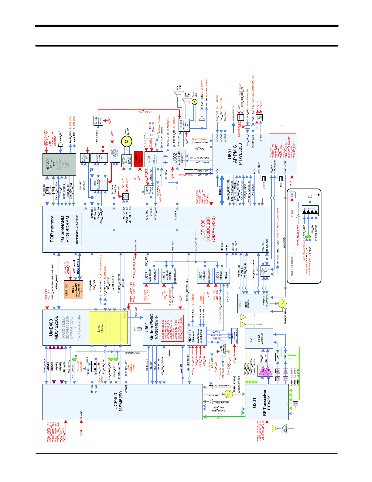
Block Diagrams
7.
block diagram
7.
7-1
SAMSUNG Proprietary-Contents may change without notice
This Document can not be used without Samsung's authorization
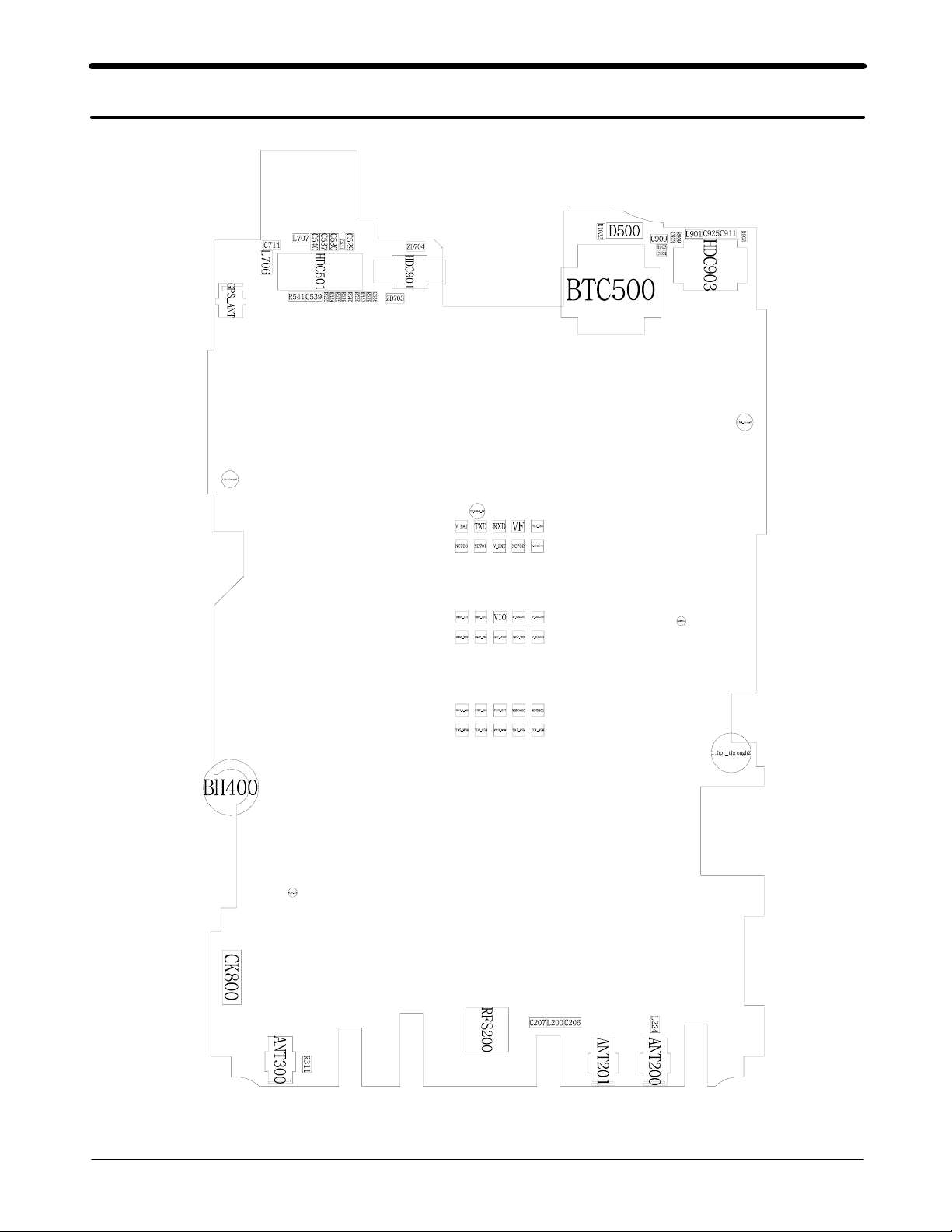
PCB Diagrams
8.
Top
8-1
SAMSUNG Proprietary-Contents may change without notice
This Document can not be used without Samsung's authorization
 Loading...