

Page 1
SERVICE
Manual
DIGITAL HOME
THEATER SYSTEM
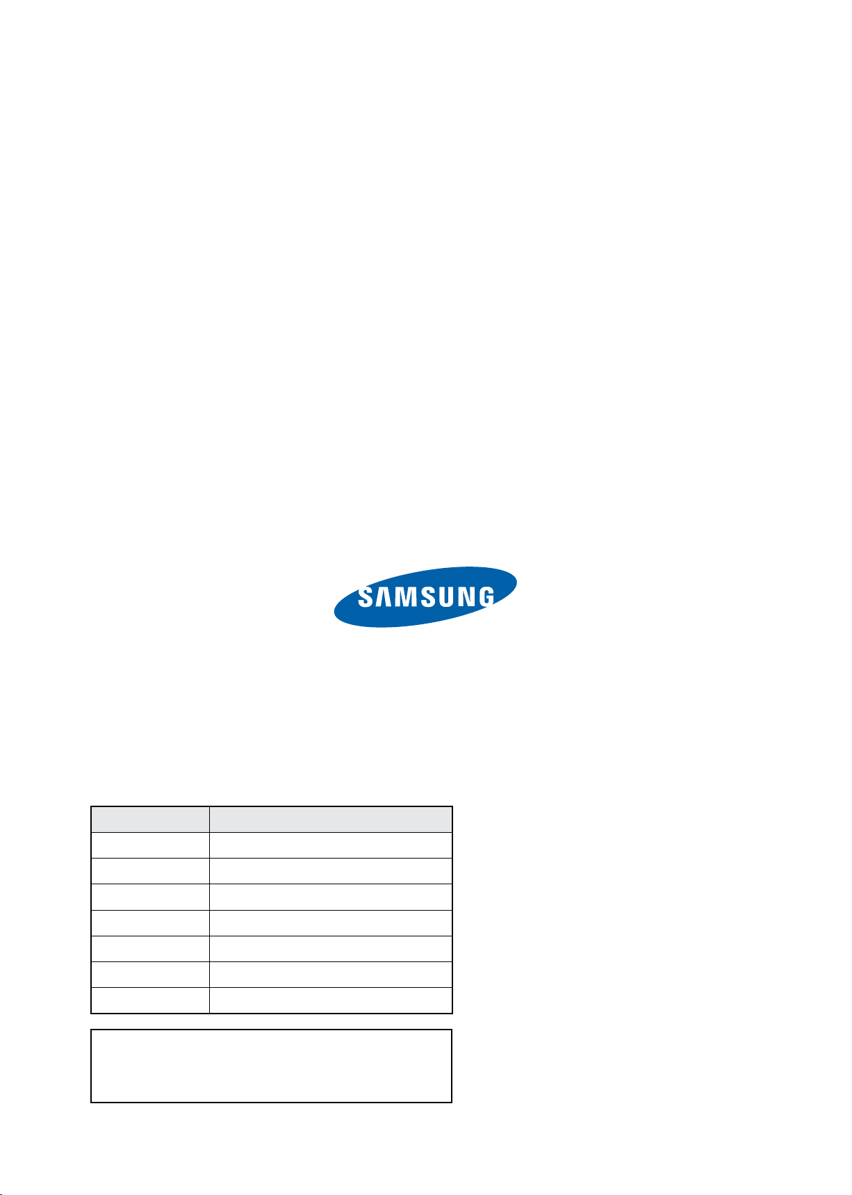
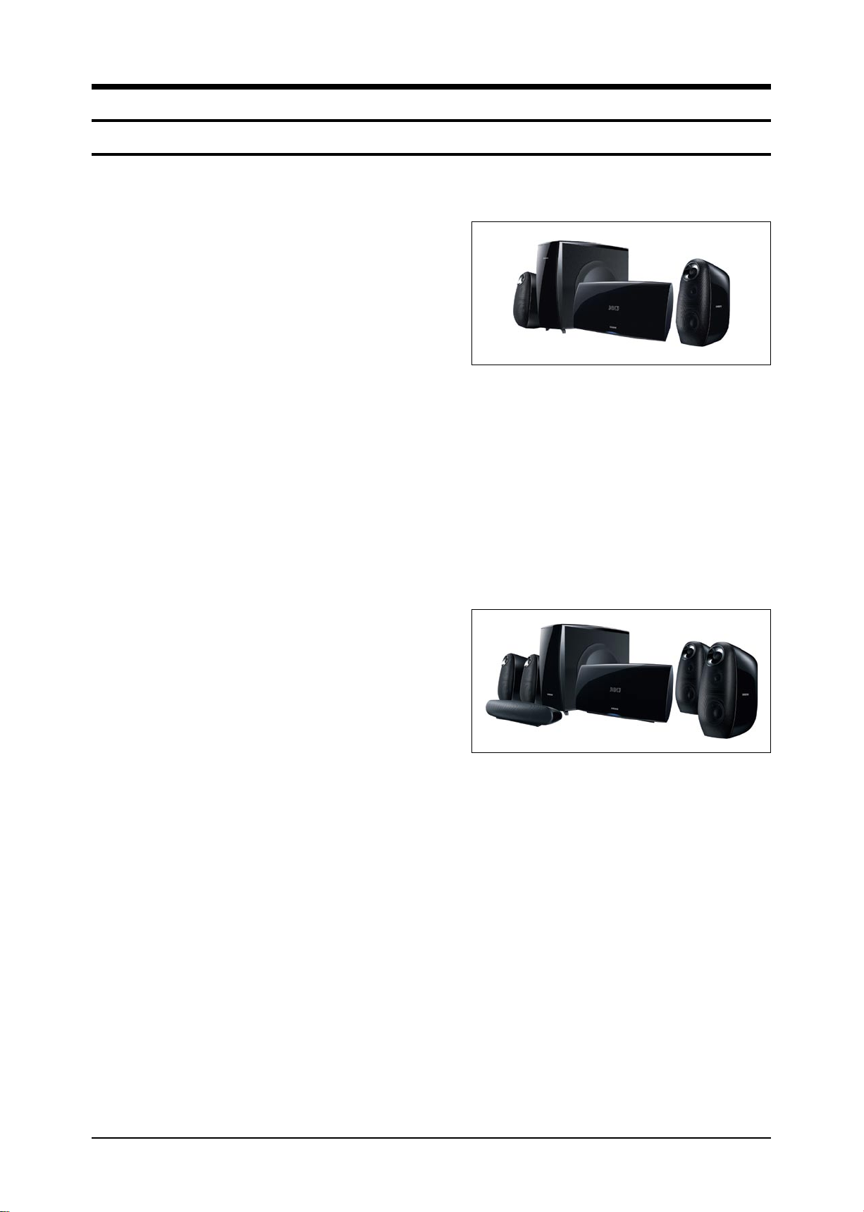
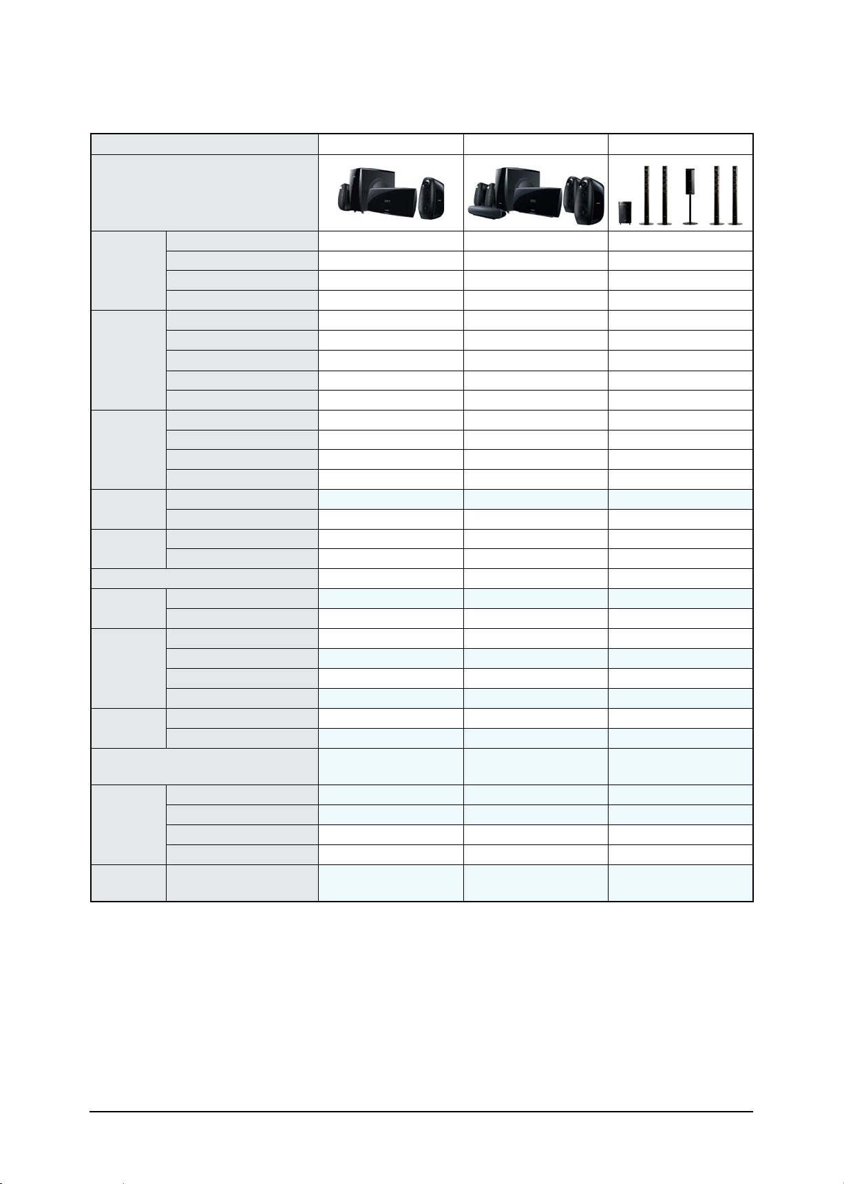
Model Name : HT-A100 / HT-XA100
Model Code : HT-A100T/XET
Speaker HT-A100
Front PS-A100
Center -
Rear -
Subwoofer PS-WA100
DIGITAL HOME THEATER SYSTEM
HT-A100
CONTENTS
1. Precaution
2. Product Specification
3. Disassembly & Reassembly
4. Troubleshooting
5. Exploded View & Part List
6. PCB Diagram
7. Schematic Diagram
Refer to the service manual in the GSPN (see the rear cover) for the more information.
Page 2
This Service Manual is a property of Samsung Electronics
Co.,Ltd. Any unauthorized use of Manual can be punished
under applicable International and/or domestic law.
GSPN (Global Service Partner Network)
Area Web Site
North America service.samsungportal.com
Latin America latin.samsungportal.com
CIS cis.samsungportal.com
Europe europe.samsungportal.com
China china.samsungportal.com
Asia asia.samsungportal.com
Mideast & Africa mea.samsungportal.com
© Samsung Electronics Co.,Ltd. Feb. 2008
Printed in Korea
Page 3

Contents
1. Precaution
1-1 Safety Precautions ...........................................................................................1-1
1-2 Servicing Precautions ......................................................................................
1-3 Precautions for Electrostatically Sensitive Devices (ESDs) .............................
2. Product Specification
2-1 Product Feature ...............................................................................................2-1
2-2 Specifications ...................................................................................................
2-3 Specifications Analysis .....................................................................................
2-4 Accessories ......................................................................................................
3. Disassembly & Reassembly
3-1 Overall Disassembly & Reassembly ................................................................3-1
1-3
1-4
2-2
2-4
2-6
4. Troubleshooting
4-1 Checkpoints by Error Mode.............................................................................. 4-2
4-2 Measures to be taken when the Protection Circuit operates ...........................
4-3 Initialization & Upgrade Methods .....................................................................
5. Exploded View & Part List
5-1 SET Exploded View .........................................................................................5-2
5-2 Speaker System ...............................................................................................
5-3 Electrical Part List ............................................................................................5-5
4-19
4-21
5-4
Page 4

Contents
6. PCB Diagram
6-1 Wiring Diagram ................................................................................................6-2
6-2 VFD PCB Top ...................................................................................................
6-3 VFD PCB Bottom .............................................................................................
6-4 AUX. SPK PCB Top .........................................................................................
6-5 AUX. SPK Bottom ............................................................................................
6-6 AMP PCB Top ..................................................................................................
6-7 AMP PCB Bottom .............................................................................................
6-8 W/LESS. OPT PCB Top ...................................................................................
6-9 W/LESS. OPT PCB Bottom .............................................................................
6-10 USB PCB Top ...................................................................................................
6-11 USB PCB Bottom .............................................................................................
6-12 KEY PCB Top ...................................................................................................
6-13 KEY PCB Bottom .............................................................................................
6-14 MAIN PCB Top .................................................................................................
6-15 MAIN PCB Bottom ...........................................................................................
6-16 BLUETOOTH PCB Top ....................................................................................
6-17 BLUETOOTH PCB Bottom ..............................................................................
6-18 POWER PCB Top ............................................................................................
6-19 POWER PCB Bottom .......................................................................................
6-20 SMPS PCB Top ................................................................................................
6-3
6-5
6-6
6-8
6-9
6-12
6-13
6-13
6-14
6-16
6-17
6-18
6-19
6-21
6-24
6-24
6-25
6-25
6-26
7. Schematic Diagram
7-1 Overall Block Diagram .....................................................................................7-2
7-2 AMP_USB ........................................................................................................
7-3 AMP_VIDEO JACK ..........................................................................................
7-4 AMP_SPK ........................................................................................................
7-5 AMP_VFD ........................................................................................................
7-6 AMP_POWER ..................................................................................................
7-7 KEY_FUNC ......................................................................................................
7-8 KEY_POWER ..................................................................................................
7-9 MAIN_MICOM ..................................................................................................
7-10 MAIN_HDMI .....................................................................................................
7-11 MAIN_DSP .......................................................................................................
7-12 MAIN_PWM .....................................................................................................
7-13 MAIN_VIDEO ...................................................................................................
7-14 MAIN_MPEG
7-15 SMPS ...............................................................................................................
....................................................................................................7-15
7-3
7-4
7-5
7-6
7-7
7-8
7-9
7-10
7-11
7-12
7-13
7-14
7-16
Page 5
Precaution
1. Precaution
Follow these safety, servicing and ESD precautions to prevent damage and protect against potential hazards such
as electrical shock and X-rays.
1-1 Safety Precautions
1. Be sure that all of the built-in protective devices are replaced.
2. When reinstalling the chassis and its assemblies, be sure to restore all protective devices, including control
knobs and compartment covers.
3. Make sure that there are no cabinet openings through which people--particularly children--might insert fingers
and contact dangerous voltages. Such openings include the spacing between the picture tube and the cabinet
mask, excessively wide cabinet ventilation slots, and improperly fitted back covers.
4. Design Alteration Warning:
Never alter or add to the mechanical or electrical design of the unit.
Example: Do not add auxiliary audio or video connectors. Such alterations might create a safety hazard.
Also, any design changes or additions will void the manufacturer’s warranty.
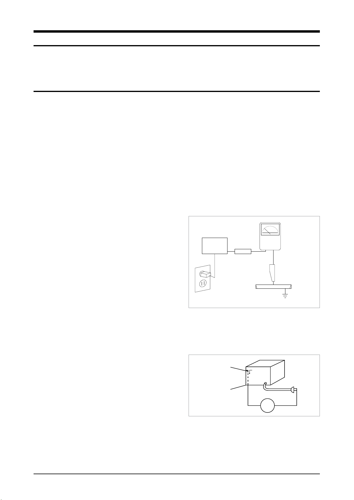
5. Leakage Current Hot Check (Fig. 1-1):
Warning: Do not use an isolation transformer during this
test. Use a leakage-current tester or a metering system
that complies with American National Standards Institute
(ANSI C101.1, Leakage Current for Appliances), and
Underwriters Laboratories (UL Publication UL1410,
59.7).
With the unit completely reassembled, plug the AC line
cord directly into a 120V AC outlet. With the unit’s AC
switch first in the ON position and then OFF, measure
the current between a known earth ground (metal water
DEVICE
UNDER
TEST
TEST ALL
EXPOSED METAL
SURFACES
2-WIRE CORD
ALSO TEST WITH
PLUG REVERSED
(USING AC
ADAPTER PLUG
AS REQUIRED)
<Fig. 1-1 AC Leakage Test>
LEAKAGE
CURRENT
TESTER
(READING
SHOULD NOT BE
ABOVE 0.5mA)
EARTH
GROUND
pipe, etc.) and all exposed metal parts. Examples:
Handle brackets, metal cabinets, screwheads and control shafts. The current measured should not exceed 0.5
milliamp. Reverse the powerplug prongs in the AC outlet and repeat.
6. Insulation Resistance Cold Check:
(1) With the unit’s AC plug disconnected from the AC
source, connect an electrical jumper across the two AC
Antenna
Terminal
prongs. (2) Set the power switch to ON. (3) Measure
the resistance between the shorted AC plug and any
exposed metallic parts.
Example: Screwheads, antenna, control shafts or handle
brackets.
Exposed
Metal Part
ohm
Ohmmeter
<Fig. 1-2 Insulation Resistance Test>
If any of the exposed metallic parts has a return path
to the chassis, the measured resistance should be between 1 and 5.2 megohms. If there is no return path, the
measured resistance should be “infinite.” If the resistance is outside these limits, a shock hazard might exist.
See Fig. 1-2
Samsung Electronics 1-1
Page 6

1-2 Samsung Electronics
Precaution
7. Components, parts and wiring that appear to have overheated or that are otherwise damaged should be
replaced with parts that meet the original specifications. Always determine the cause of damage or overheating,
and correct any potential hazards
8. Observe the original lead dress, especially near the following areas: Antenna wiring, sharp edges, and
especially the AC and high voltage power supplies. Always inspect for pinched, out-of-place, or frayed wiring.
Do not change the spacing between components and the printed circuit board. Check the AC power cord for
damage. Make sure that no wires or components touch thermally hot parts.
9. Product Safety Notice:
Some electrical and mechanical parts have special safety-related characteristics which might not be obvious
from visual inspection. These safety features and the protection they give might be lost if the replacement
component differs from the original--even if the replacement is rated for higher voltage, wattage, etc.
10. Components that are critical for safety are indicated in the circuit diagram by shading,
or . Use
replacement components that have the same ratings, especially for flame resistance and dielectric strength
specifications. A replacement part that does not have the same safety characteristics as the original might
create shock, fire or other hazards.
Page 7
Precaution
1-2 Servicing Precautions
1. Servicing precautions are printed on the cabinet. Follow them.
2. Always unplug the unit’s AC power cord from the AC power source before attempting to: (a) Remove or reinstall
any component or assembly, (b) Disconnect an electrical plug or connector, (c) Connect a test component in
parallel with an electrolytic capacitor.
3. Some components are raised above the printed circuit board for safety. An insulation tube or tape is sometimes
used. The internal wiring may be clamped to prevent contact with thermally hot components. Reinstall all such
elements to their original position.
4. After servicing, always check that the screws, components and wiring have been correctly reinstalled.
Make sure that the portion around the serviced part has not been damaged.
5. Check the insulation between the blades of the AC plug and accessible conductive parts (examples: metal
panels, input terminals and earphone jacks).
6. Insulation Checking Procedure: Disconnect the power cord from the AC source and turn the power switch ON.
Connect an insulation resistance meter (500V) to the blades of the AC plug.
The insulation resistance between each blade of the AC plug and accessible conductive parts (see above)
should be greater than 1 megohm.
7. Never defeat any of the B+ voltage interlocks. Do not apply AC power to the unit (or any of its assemblies)
unless all solid-state heat sinks are correctly installed.
8. Always connect a test instrument’s ground lead to the instrument chassis ground before connecting the positive
lead; always remove the instrument’s ground lead last.
First read the “Safety Precautions” section of this manual. If some unforeseen circumstance
creates a conflict between the servicing and safety precautions, always follow the safety
precautions.
Samsung Electronics 1-3
Page 8

Precaution
1-3 Precautions for Electrostatically Sensitive Devices (ESDs)
1. Some semiconductor (“solid state”) devices are easily damaged by static electricity.
Such components are called Electrostatically Sensitive Devices (ESDs). Examples include integrated circuits
and some field-effect transistors. The following techniques will reduce the occurrence of component damage
caused by static electricity.
2. Immediately before handling any semiconductor components or assemblies, drain the electrostatic charge from
your body by touching a known earth ground. Alternatively, wear a discharging wrist-strap device. (Be sure to
remove it prior to applying power--this is an electric shock precaution.)
3. After removing an ESD-equipped assembly, place it on a conductive surface such as aluminum foil to prevent
accumulation of electrostatic charge.
4. Do not use freon-propelled chemicals. These can generate electrical charges that damage ESDs.
5. Use only a grounded-tip soldering iron when soldering or unsoldering ESDs.
6. Use only an anti-static solder removal device. Many solder removal devices are not rated as “anti-static” (these
can accumulate sufficient electrical charge to damage ESDs).
7. Do not remove a replacement ESD from its protective package until you are ready to install it.
Most replacement ESDs are packaged with leads that are electrically shorted together by conductive foam,
aluminum foil or other conductive materials.
8. Immediately before removing the protective material from the leads of a replacement ESD, touch the protective
material to the chassis or circuit assembly into which the device will be installed.
9. Minimize body motions when handing unpackaged replacement ESDs. Motions such as brushing clothes
together, or lifting a foot from a carpeted floor can generate enough static electricity to damage an ESD.
1-4 Samsung Electronics
Page 9
2. Product Specification
2-1 Product Feature
2-1-1 HT-A100 Product Feature
300W Power
2.1 CH HTiB
- Virtual 5.1 Ch Surround
HDMI /w 1080P up-scale
- Anynet+ (HDMI CEC)
Bluetooth (USA Only)
USB Host w/ video playback
DVD-Audio Playback
Product Specification
2 way 2 speaker
2-1-2 HT-XA100 Product Feature
600W Power
5.1 CH HTiB
HDMI /w 1080P up-scale
- Anynet+ (HDMI CEC)
Bluetooth (USA Only)
USB Host w/ video playback
DVD-Audio Playback
2 way 2 speaker
Samsung Electronics 2-1
Page 10
2-2 Samsung Electronics
Product Specification
2-2 Specifications
Basic Specification
Model Name HT-A100 / HT-XA100
Power Requirements AC 220V, 60Hz
General
Disc
Video
Output
Power Consumption
Weight 8.8 Ibs
Dimensions 18.5 (W) x 4.6 (H) x 7.7 (D) inches
Operating Temperature Range
Operating Humidity Range
DVD (Digital Versatile Disc)
CD: 5 inches
(COMPACT DISC)
CD: 3 1/2 inches
(COMPACT DISC)
Composite Video
Component Video
55 W
+41°F to +95°F
10 % to 75 %
Reading Speed: 3.49 ~ 4.06 m/sec.
Approx. Play Time (Single Sided, Single Layer Disc): 135 min.
Reading Speed: 4.8 ~ 5.6 m/sec.
Maximum Play Time: 74 min.
Reading Speed: 4.8 ~ 5.6 m/sec.
Maximum Play Time: 20 min.
1.0 Vp-p (75 Ω load)
Y: 1.0 Vp-p (75 Ω load)
PR: 0.70 Vp-p (75 Ω load)
PB: 0.70 Vp-p (75 Ω load)
Amplifier
HDMI Impedance: 85~115Ω
Front speaker output
Center speaker output
Rear speaker output
Subwoofer speaker output
Frequency range
S/N Ratio
Channel separation
Input sensitivity
100W x 2 (3Ω)
100W (3Ω)
100W x 2 (3Ω)
100W (3Ω)
20Hz ~ 20KHz
70dB
60dB
(AUX) 400mV
Page 11
Samsung Electronics 2-3
Product Specification
HT-A100 Speaker Specification
Speaker system
Impedance 3 Ω 3 Ω
Frequency range
Output sound pressure level
Speaker
Rated input
Maximum input
Dimensions (W x H x D)
Weights
HT-XA100 Speaker Specification
Speaker system
2.1ch speaker system
Front Subwoofer
140Hz ~ 20KHz 35Hz ~ 160Hz
86dB 86dB
100W 100W
200W 200W
Front: 4.25 x 9.68 x 8.58 inches
Subwoofer: 7.09 x 15.3 x 15.59 inches
Front: 2.43 lbs
Subwoofer: 14.1 lbs
5.1ch speaker system
Front/Center/Rear Subwoofer
Speaker
Impedance 3 Ω 3 Ω
Frequency range
Output sound pressure level
Rated input
Maximum input
Dimensions (W x H x D)
Weights
140Hz ~ 20KHz 35Hz ~ 160Hz
86dB 86dB
100W 100W
200W 200W
Front/Rear: 4.25 x 9.68 x 8.58 inches (Stand Base: Ø14inch)
Center: 14.8 x 3.29 x 5.59 inches
Subwoofer: 7.09 x 15.3 x 15.59 inches
Front: 2.43 lbs, Rear: 2.09 lbs
Center: 2.64 lbs, Subwoofer: 14.1 lbs
Page 12
2-4 Samsung Electronics
Product Specification
2-3 Specifications Analysis
Model Name
Photo
Output
Power
General
Compatible
A/V
DVD (Video)
Sound Mode
SDSM-EX (DNSE 5.1) X X X
Audio
Decoding
RMS (10% THD), REF: 1CH
Output Power (ch)
HDMI CEC
Calliope X X X
Deck Slot In Slot In Slot In
DVD Disc Capacity
Front Display
Sleep
Dimmer
CD/CD-R/CD-RW
VCD/SVCD
DVD/DVD-R/DVD-RW
MP3
JPEG Viewer
DVD-Audio
DVD-OK
WMA
DIVX
SACD
WIRELESS
USB HOST
Anynet Anynet+ Anynet+ Anynet+
Progressive Scan (NT/PAL)
Logo copy
NTSC ↔ PAL
PAL M (Brazil)
EQ/DSP X 3Mode / 5Mode 3Mode / 5Mode
POWER BASS
VIRTUAL SOUND
Dolby Digital
Dolby ProLogic-II
Dolby ProLogic-IIX
DTS
Dolby Digital EX
DTS ES Discrete 6.1
DTS 96/24
THX X X X
DTS Neo 6
AVI
WMV
HT-A100 HT-XA100 HT-TX500
300W 600W 1000W
100W x 3 100W x 6
1 DVD 1 DVD 1 DVD
1Color - VFD 1Color - VFD 1Color - VFD
(except USA, EU) (except USA, EU) (except USA, EU)
(except CIS) (except CIS) (except CIS)
X X
Divx3.11~Divx5.1, XviD Divx3.11~Divx5.1, XviD
V1/V2/V3/V7 V1/V2/V3/V7
X X X
X
(USA only NTSC) (USA only NTSC) (USA only NTSC)
(USA only NTSC, CIS
only PAL)
X X X
X
X X X
X X X
X X X
X X X
X X X
(USA only NTSC, CIS
only PAL)
X X
167W x 5
(Active Subwoofer: 165W)
(4000 Songs, only CIS)
(USA only NTSC, CIS
only PAL)
X
: application, X: non-application
Page 13
Samsung Electronics 2-5
Product Specification
Video Inputs
Video
Outputs
Audio in/out
Optical jack
Coaxial jack
Headphone/
MIC Jack
Tuner
Remote Key
Speaker
Net Weight
(Kg)
Model Name
Photo
Component X X X
Composite X X X
S-Video X X X
HDMI In
Component
Composite
HDMI Out
S-Video X X X
SCART Out
In
Line In
Multi ch Out
Out X X X
In (Digital In)
Out X X X
In X X X
Out X X X
i-Link X X X
Headphone Jack (3.5Φ)
2 MIC Jack (6.5Φ) X X X
FM
RDS
AM
Preset Memory
Universal (MBR)
Key 54 Key 60 Key 60 Key
Dual Voltage
Type (Sat/Tallboy)
Stand X X
Impedance (Sat/Woofer)
Active (Powered) S/W
Set 4 4 5
HT-A100 HT-XA100 HT-TX500
X X X
(1080P) (1080P) (1080P)
X X X
AUX1 AUX1 AUX1
AUX2 AUX2 AUX2
X X X
(*1) (*1) (*2)
X X
X X X
15 15 X
FREE VOLTAGE
(HIGH, LOW)
Satellite Satellite Tallboy
3Ω/3Ω 3Ω/3Ω 3Ω/3Ω
X X X
FREE VOLTAGE
(HIGH, LOW)
(EU Only)
HIGH, LOW, DUAL Voltage
X
: application, X: non-application
Page 14
Product Specification
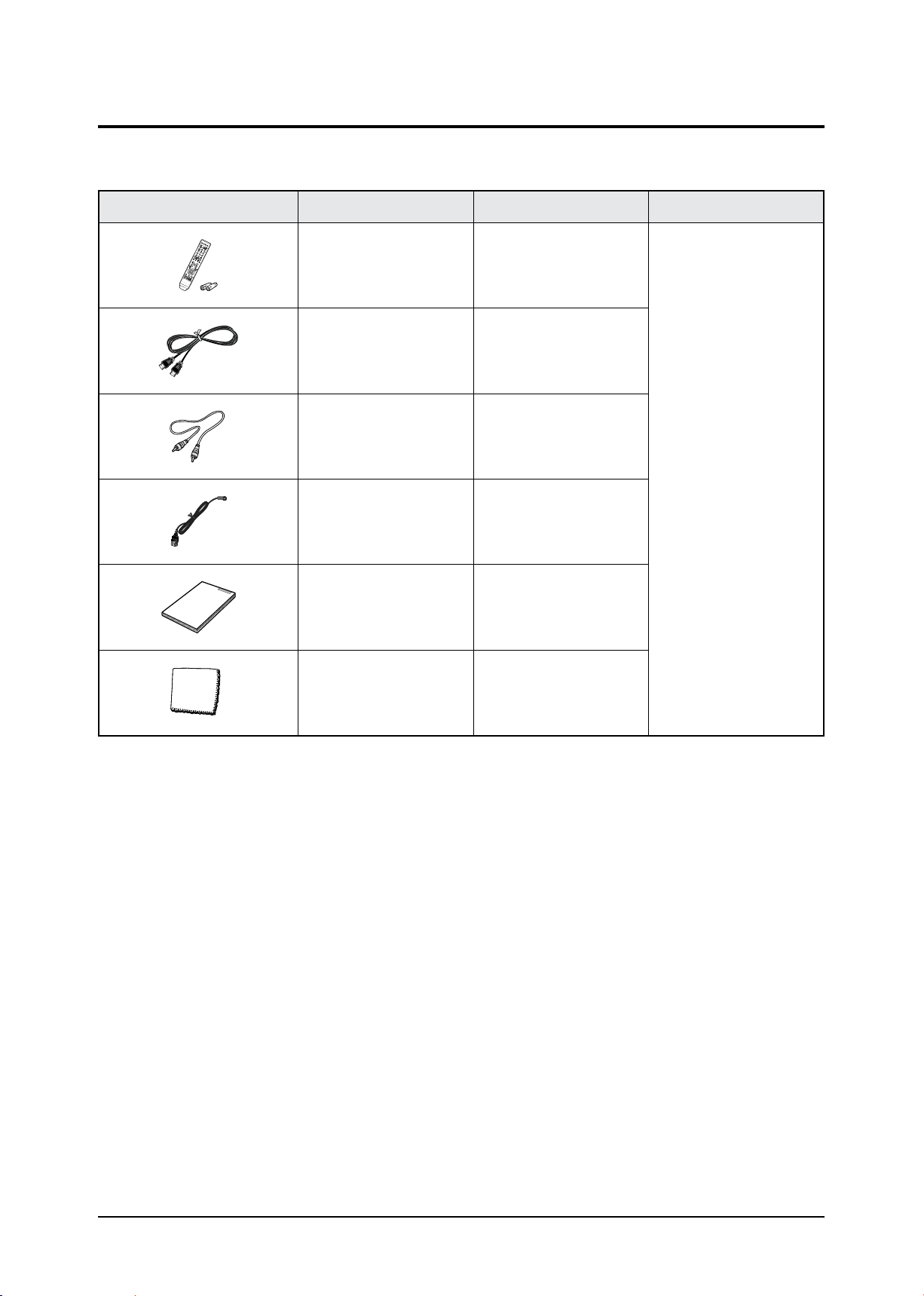
2-4 Accessories
2-4-1 Supplied Accessories
Accessories Item Item code Remark
Remote Control
Batteries
HDMI Cable AH39-00721A
Video Cable AH39-40001V
FM Antenna AH42-00021A
Owner’s Instructions AH68-02056D
AH59-01907G
4301-000116
Samsung Service center
Cloth Clean AH81-02286C
2-6 Samsung Electronics
Page 15
Disassembly & Reassembly
3. Disassembly & Reassembly
3-1 Overall Disassembly & Reassembly
- Be careful to follow the disassembly sequence described in the manual. Otherwise, the product
may be damaged.
- Be sure to carefully read and understand the safety instructions before performing any work as
the IC chips on the PCB are vulnerable to static electricity.
- Assemble in the reverse order of disassembly.
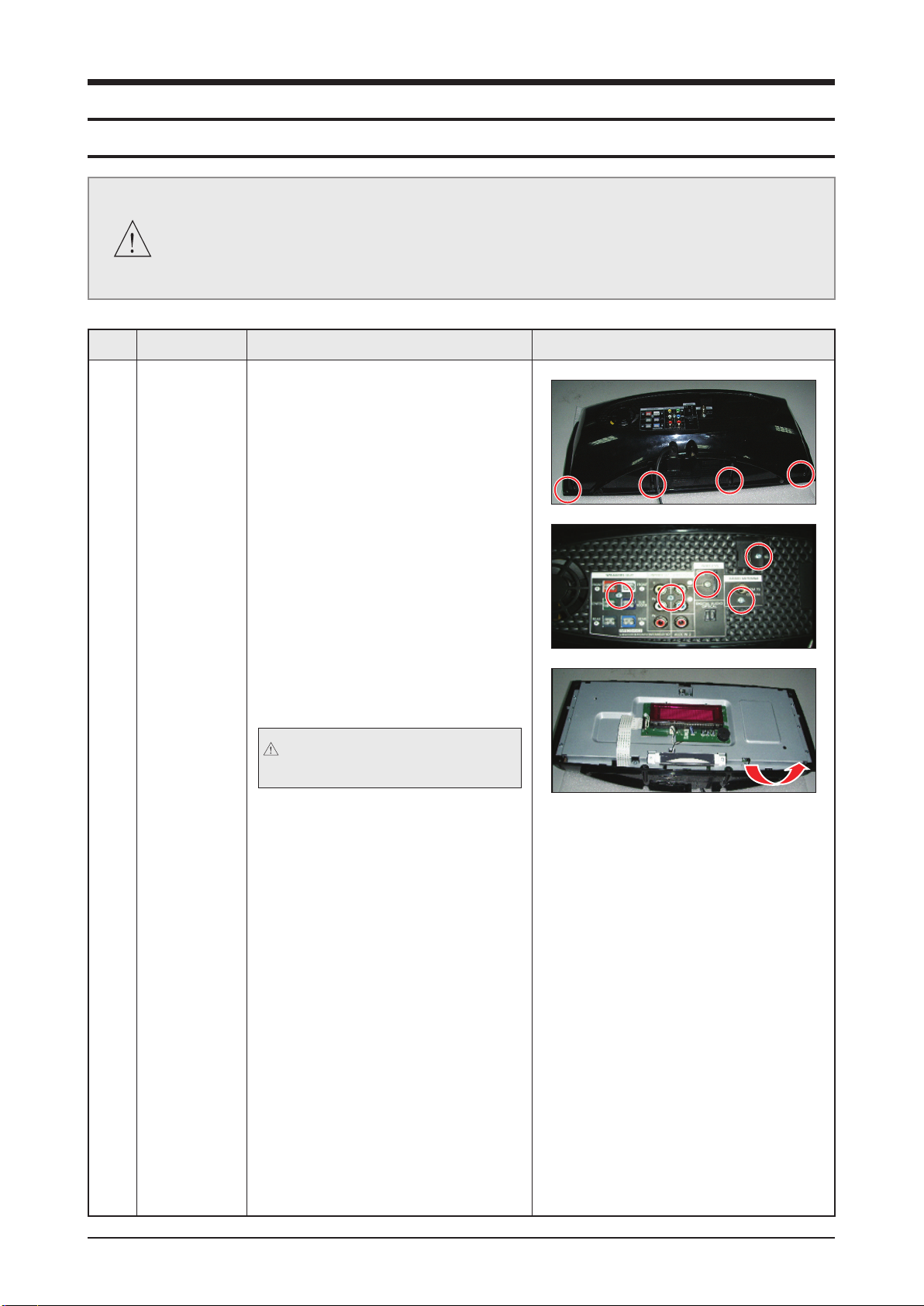
No. Part Name Description Description Photo
1 CABINET-
FRONT
1) Remove the 4 screws from the
bottom of CABINET-REAR.
: M3X10,BLACK
2) Remove the 4 or 5 screws from the
DECO-REAR.
: M3X10,BLACK
3) Lift the CABINET-FRONT up to
separate it.
Be careful not to make any
scratches as you remove it.
Samsung Electronics 3-1
Page 16
3-2 Samsung Electronics
Disassembly & Reassembly
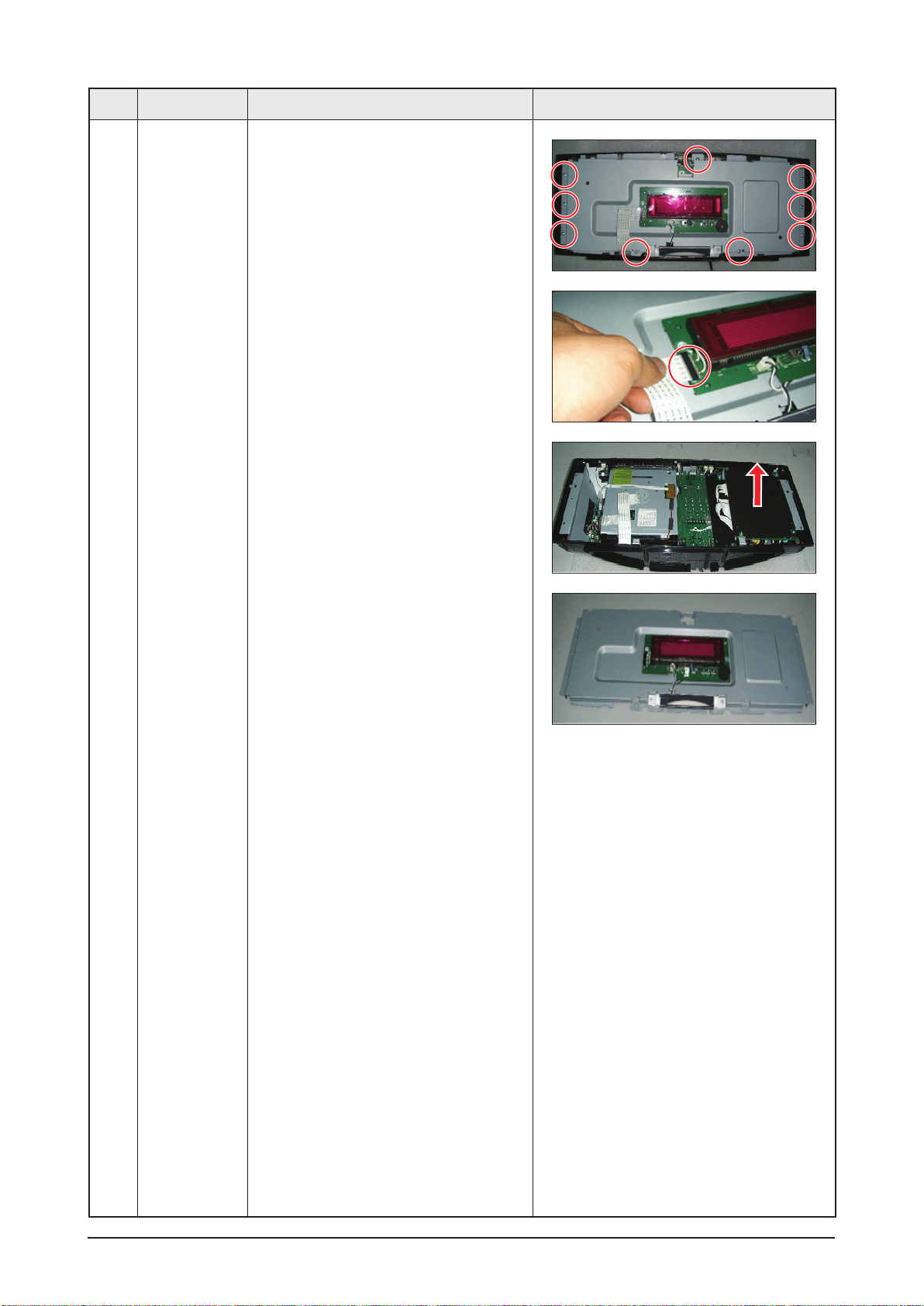
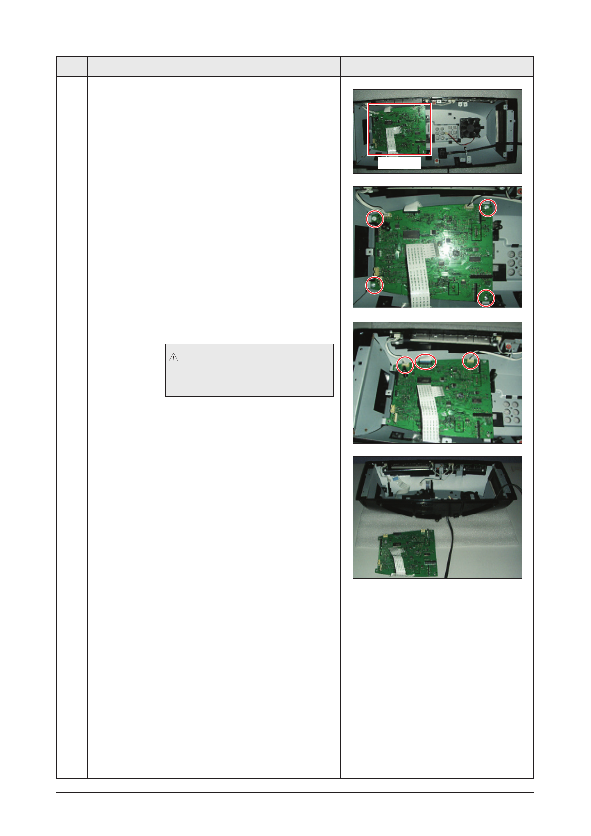
No. Part Name Description Description Photo
2 ASSY
SHEILD-
FRONT
/
PCB-VFD
1) Remove the 9 screws.
: M3X10,WHITE
2) Disconnect the Flat-Cable connected
to PCB-VFD.
3) Lift the ASSY SHIELD-FRONT up to
separate it.
Page 17
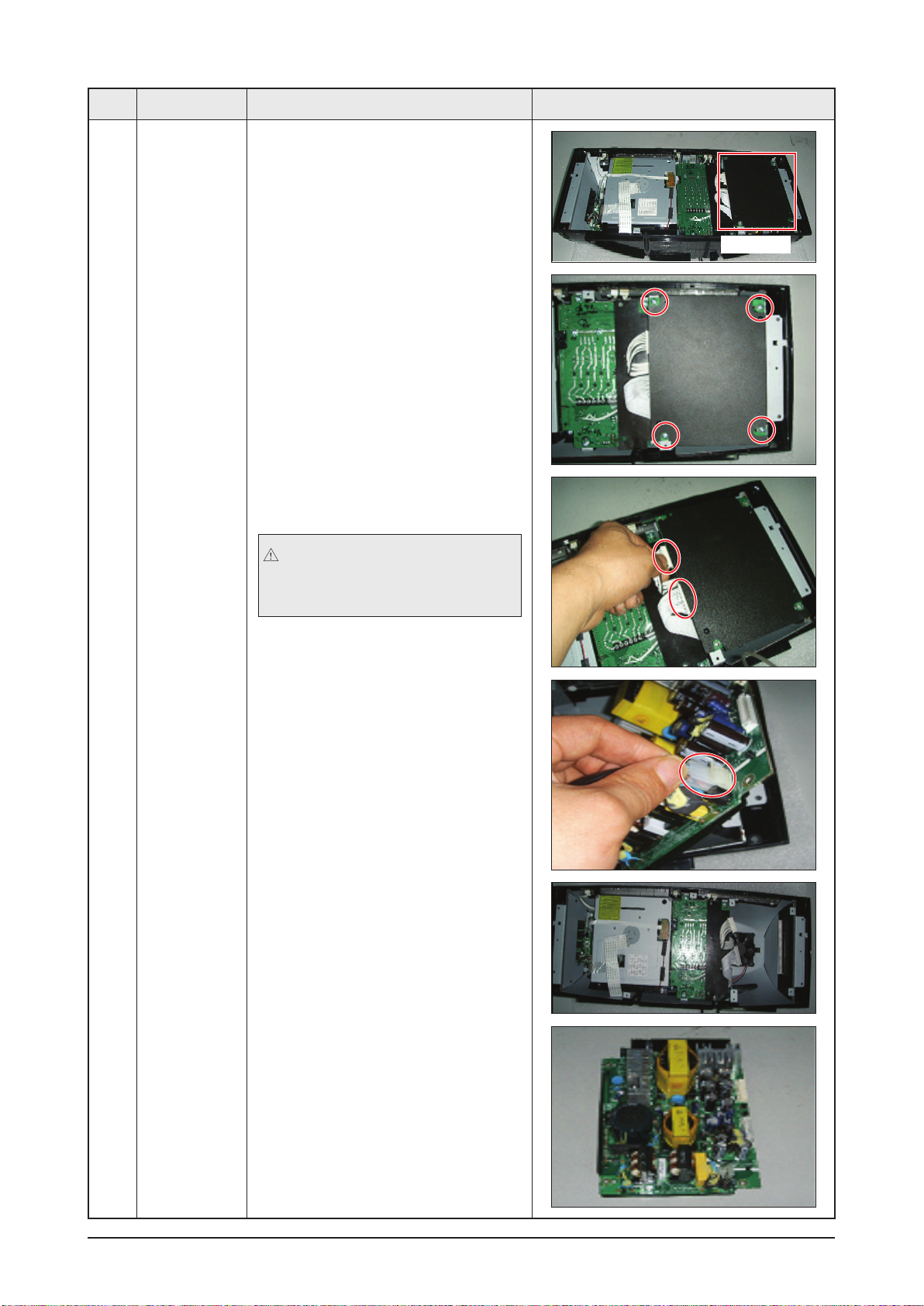
Disassembly & Reassembly
No. Part Name Description Description Photo
3 PCB-SMPS 1) Remove the 4 screws.
: M3X10,WHITE
PCB-SMPS
2)
Separate the 2 cables connected to
PCB-AMP.
In case of pulling up the PCB
cable, it is easier to pull up when
pressing the grip.
3) Separate the POWER-CABLE.
4)
Lift the PCB-SMPS up to separate it.
Samsung Electronics 3-3
Page 18
3-4 Samsung Electronics
Disassembly & Reassembly
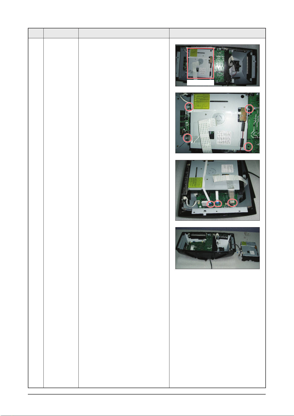
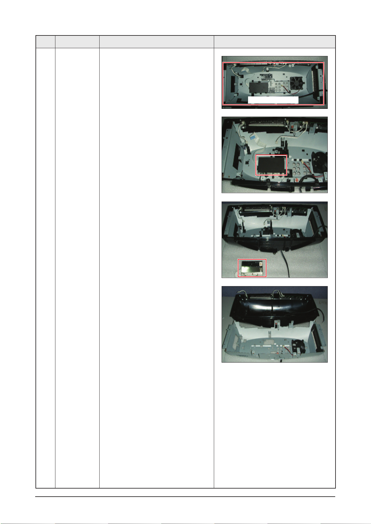
No. Part Name Description Description Photo
4 SLOT-
MECHA
1) Remove the 4 screws.
: M3X10,WHITE
SLOT-MECHA
2) Disconnect the 3 Flat-Cables
connected to PCB-MAIN.
3) Lift the SLOT-MECHA up to separate
it.
Page 19
Disassembly & Reassembly
No. Part Name Description Description Photo
5 PCB-AMP 1) Remove the 4 screws.
: M3X10,WHITE
2) Separate the 3 cables.
In case of pulling up the PCB
cable, it is easier to pull up when
pressing the grip.
PCB-AMP
3) Separate the cable of FAN after lifting
the PCB-AMP.
4) Lift the PCB-AMP completely to
separate it.
Samsung Electronics 3-5
Page 20
3-6 Samsung Electronics
Disassembly & Reassembly
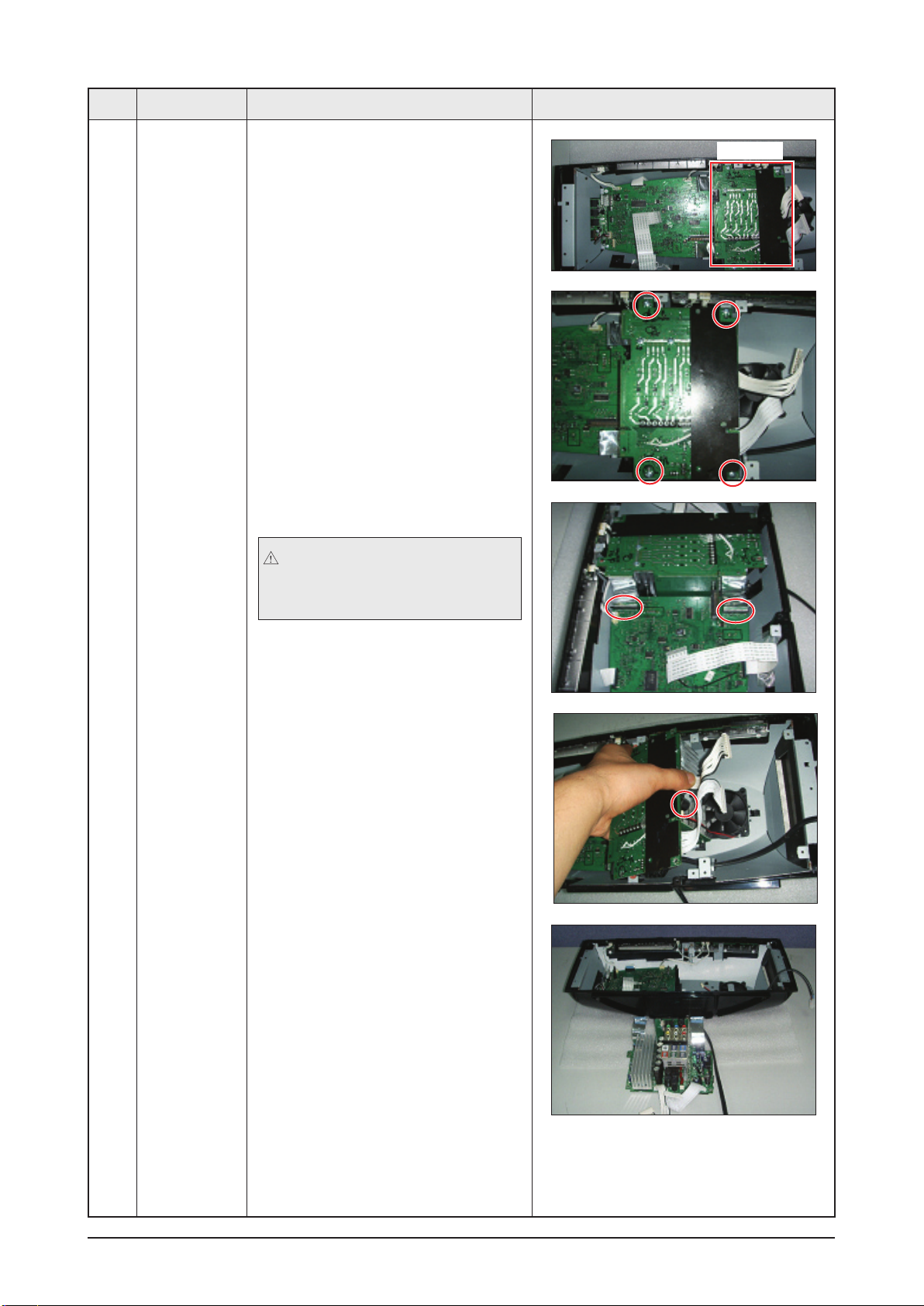
No. Part Name Description Description Photo
6 PCB-USB 1) Remove the screw from the
PCB-USB.
: M3X10,WHITE
PCB-USB
2) Disconnect the 2 cables connected to
PCB-MAIN.
In case of pulling up the PCB
cable, it is easier to pull up when
pressing the grip.
3) Lift the PCB-USB up to separate it.
Page 21
Disassembly & Reassembly
No. Part Name Description Description Photo
7 PCB-MAIN 1) Remove the 4 screws.
: M3X10,WHITE
PCB-MAIN
2) Separate the 3 cables.
In case of pulling up the PCB
cable, it is easier to pull up when
pressing the grip.
3) Lift the PCB-MAIN up to separate it.
Samsung Electronics 3-7
Page 22
Disassembly & Reassembly
No. Part Name Description Description Photo
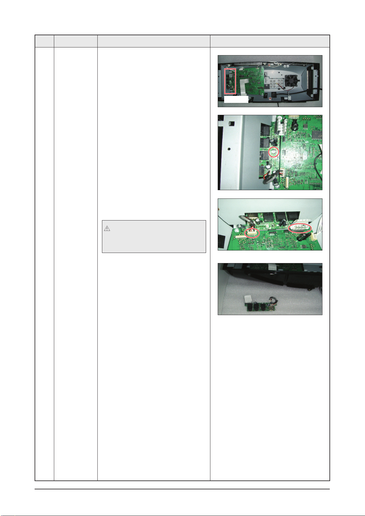
8 ASSY
SHEILD-
REAR
1) Separate FM MODULE and
SHIELD-REAR.
ASSY SHEILD-REAR
2) Lift the SHIELD-REAR up to separate
it.
3-8 Samsung Electronics
Page 23

Troubleshooting
4. Troubleshooting
4-1 Checkpoints by Error Mode ................................................................4-2
4-2 Measures to be taken when the Protection Circuit operates ...........
4-3 Initialization & Upgrade Methods ........................................................
4-19
4-21
Samsung Electronics 4-1
Page 24
4-2 Samsung Electronics
Troubleshooting
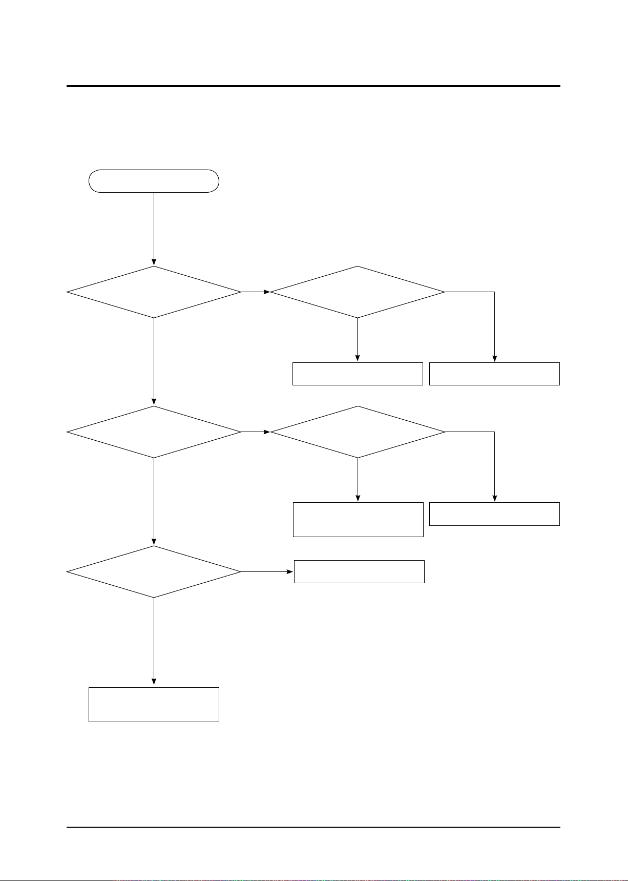
4-1 Checkpoints by Error Mode
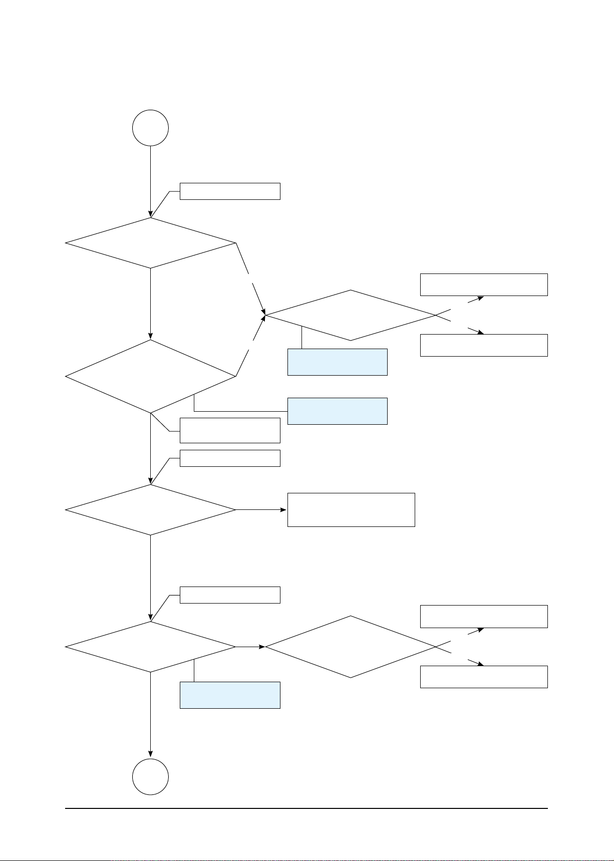
4-1-1 Power Failure
The power does not turn on.
UIC1 Main PCB;
pin 14, 40, 55, 89 5V?
Yes
Check for
POWER-SENSE (5V) at Main PCB
: pin 26 of UIC1?
Yes
Check for
Power-ON (0V) at Main PCB;
pin 38 of UIC1
No
No
No
Micom Power +5.6V
CN2 (Pin 22) CHECK → 5.6V?
Yes
Check Pattern +5.6V Line
Power Sense,
CN2 (Pin 1) CHECK → 5V?
Yes
Check pattern Power Sense
Line
Replace Micom (UIC1)
No
Replace SMPS
No
Replace SMPS
Yes
Check for connector from Main
PCB to Front PCB; ZCON1
Page 25
Samsung Electronics 4-3
Troubleshooting
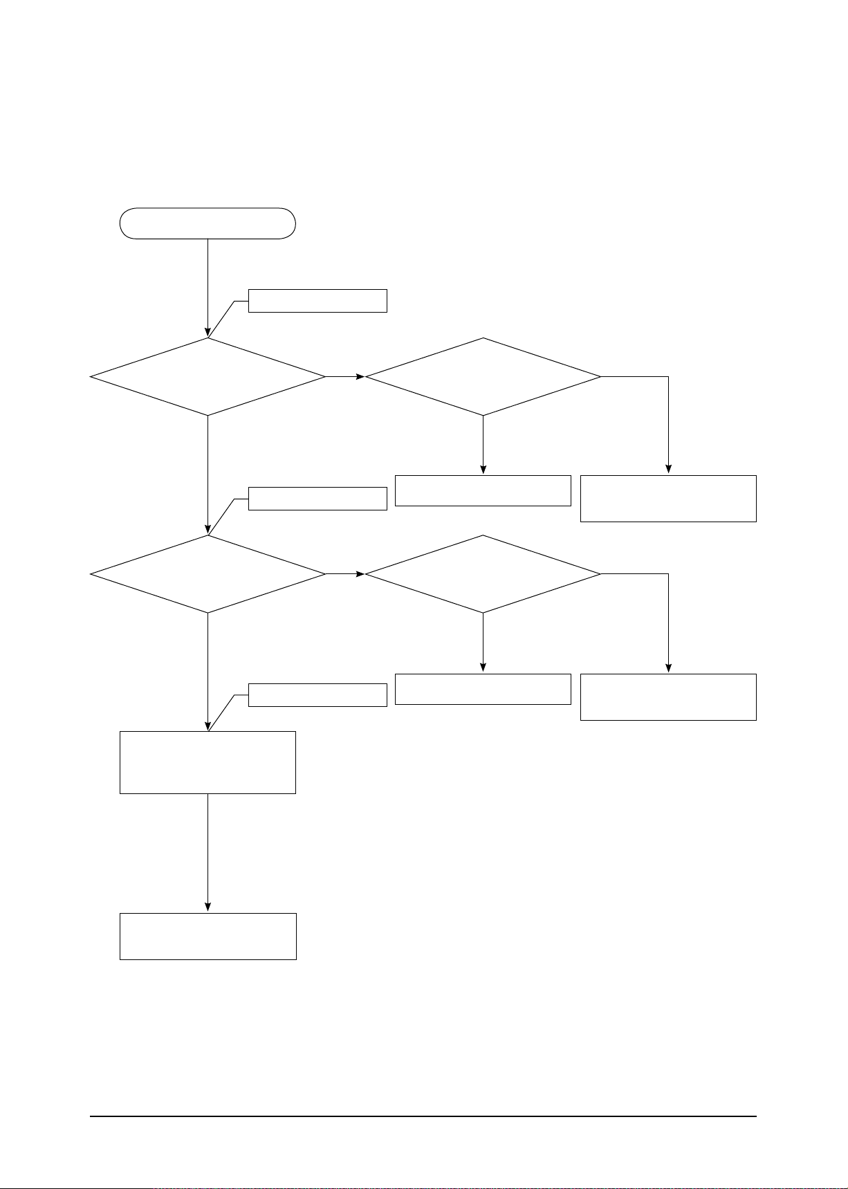
4-1-2 No Sound (waveform when 1KHz, -20dB signal is input)
No Sound
CHECK POWER
PVDD (+32V),
+12V, -12V CHECK
AMP PCB (AJ1)
Yes
AIC1 (CS5345)
AUX2: pin 7, 8
AUX1: pin 9, 10
TUNER: pin 11, 12
Yes
AIC1 (CS5345)
pin 41 CHECK
Yes
No
ADC INPUT CHECK
No
ADC OUTPUT CHECK
No
No
Replace SMPS
Check AUX1, AUX2 JACK
Pattern
AIC1 (CS5345)
power pin 36, 30, 14 (5V),
46 (3.3V) check
AIC1 (CS5345)
control pin 1, 2, 3, 4, 6
check
Check 5V, 3.3V Pattern
No
Yes
Replace AIC1
Yes
No
Check AIC1’s Control Line
Pattern
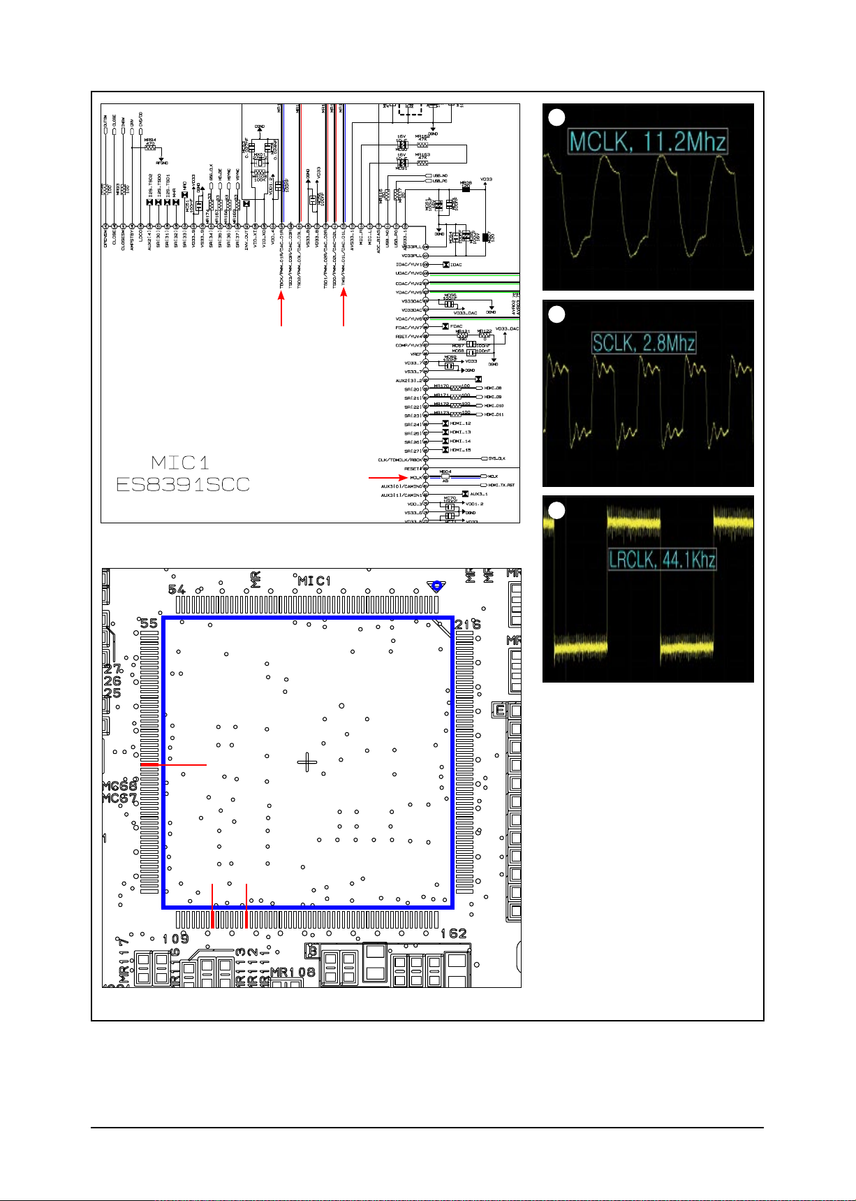
MIC1 (ES8391)
pin 65 CHECK
Yes
A
MPEG INPUT CHECK
No
Check AIC1 & MIC1 Data Line
Pattern
Page 26
4-4 Samsung Electronics
Troubleshooting
pin 117, 118, 121 CHECK
A
ADC OUTPUT CHECK
MIC1 (ES8391)
Yes
MIC1 (ES8391)
pin 82 (MCLK),
pin 116 (LRCK),
pin 123 (SCLK)
CHECK
Yes
U1 (PS9829B)
pin 15, 16, 17 CHECK
Yes
No
No
LRCK, SCLK, MCLK
CHECK
PWM INPUT CHECK
No
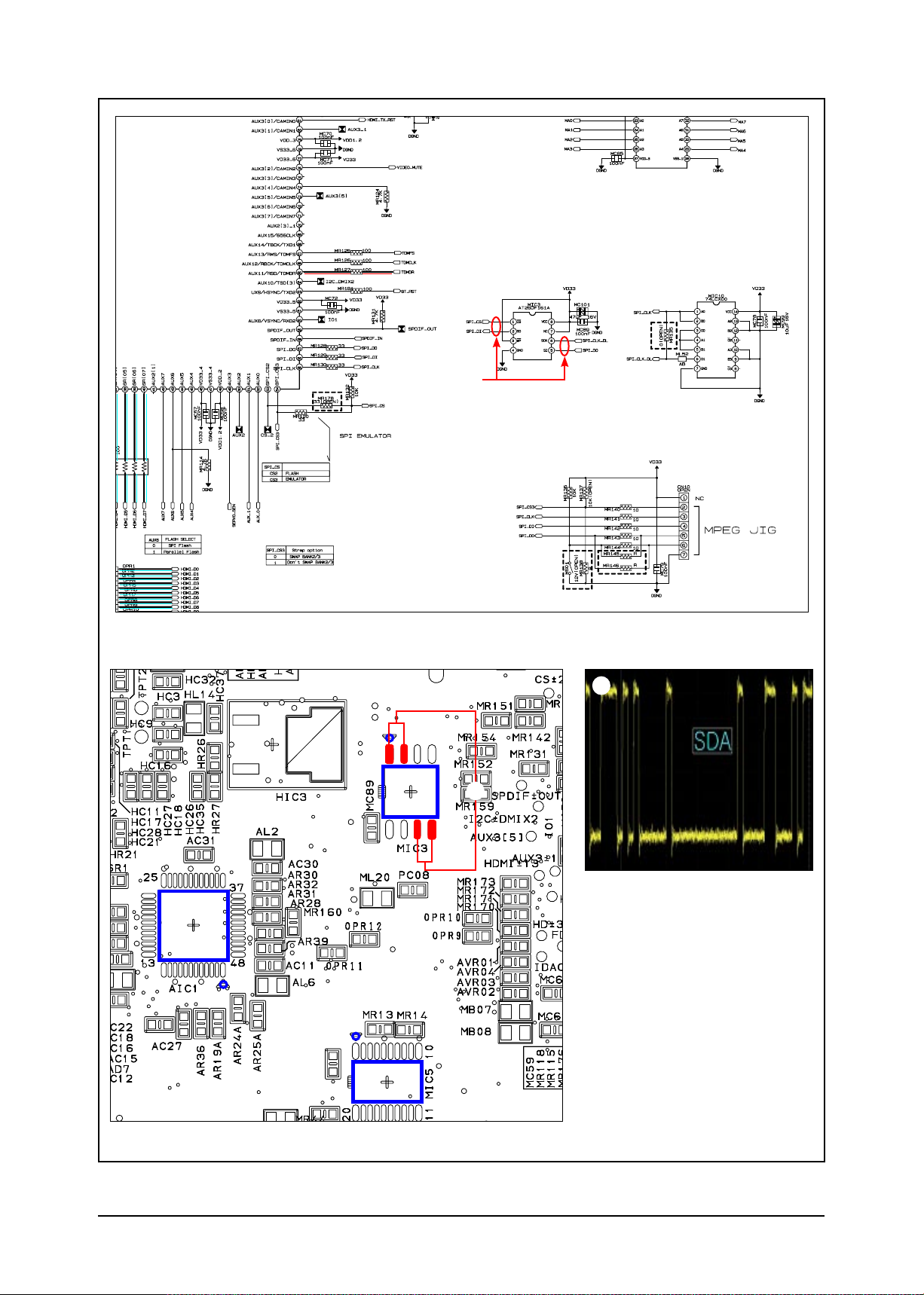
MIC3 (AT26DF161A)
Control Pin 1, 2, 5, 6 CHECK
Refer to wave pattern
image of Fig. 4-2.
Refer to wave pattern
image of Fig. 4-1.
Check MIC1 & U1 Data Line
Pattern
Replace MIC3
No
Yes
Replace MIC1
PWM OUTPUT CHECK
Check U1’s Power pin pattern
U1 (PS9829B)
pin 48, 49, 51, 52, 54, 55, 58, 59,
61, 62, 67, 68 CHECK
Yes
Refer to wave pattern
image of Fig. 4-3.
B
No
U1 (PS9829B)
POWER (3.3V) pin 4,10, 22,
29, 39, 47, 56, 65, 72, 84, 87,
94 CHECK
No
Yes
Replace U1
Page 27
Samsung Electronics 4-5
Troubleshooting
B
AMP IC OUTPUT
CHECK
AIC 6, 7, 8 (TAS5142)
pin 22, 25, 30, 33 CHECK
Yes
Refer to wave pattern
image of Fig. 4-4-1
and Fig. 4-4-2.
SOUND OUTPUT OK (SPK01)
Refer to wave pattern
image of Fig. 4-5.
No
AIC 6, 7, 8 (TAS5142)
POWER (+12V) pin 1, 18, 19,
36 CHECK
Page 28
4-6 Samsung Electronics
Troubleshooting
RIC4
RIC1
MIC1
DIC1
DIC2
CN09
1
2
23
3
MAIN_MPEG Page, 7-15
1
213
MAIN PCB Top Page, 6-19
<Fig. 4-1>
Page 29
Samsung Electronics 4-7
Troubleshooting
MIC2
CN9
CN1
MIC3
MIC5
HPIC1
MIC6
AIC1
4
MAIN_MPEG Page, 7-15
4
4
MAIN PCB Bottom Page, 6-21
<Fig. 4-2>
Page 30
4-8 Samsung Electronics
Troubleshooting
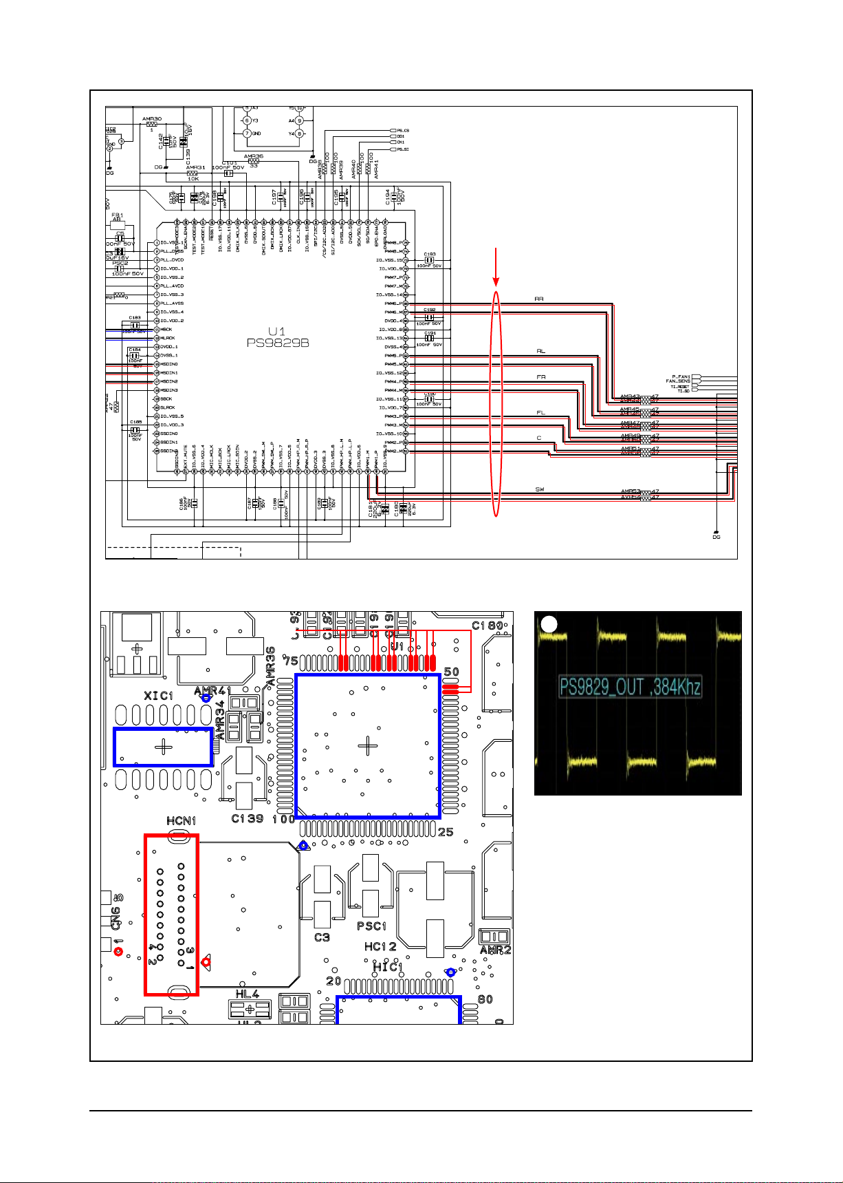
U1
XIC1
DIC1
HCN1
5
5
MAIN_PWM Page, 7-13
5
MAIN PCB Top Page, 6-19
<Fig. 4-3>
Page 31

Samsung Electronics 4-9
Troubleshooting
6
<Fig. 4-4-1>
6
6
AMP_POWER Page, 7-7
Page 32

4-10 Samsung Electronics
Troubleshooting
AIC8
AIC6
AIC7
AJ1
6
6
AMP PCB Top Page, 6-9
<Fig. 4-4-2>
Page 33
Samsung Electronics 4-11
Troubleshooting
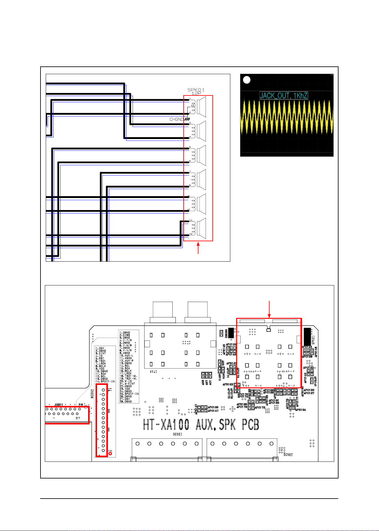
WCON2
SPK01
7
7
AMP_SPK Page, 7-5
7
AUX. SPK PCB Top Page, 6-6
<Fig. 4-5>
Page 34
4-12 Samsung Electronics
Troubleshooting
4-1-3 No Analog Video Output
COMPOSIT (VIDEO OUT)
COMPOSIT (VIDEO OUT)
Check MPEG Output.
Check if VDAC
output is measured at the pin 100 of
MIC1 ES8391.
Yes
Check Video Switch.
Check if output
is measured at the pin of 1 of JIC01
LA73054.
Yes
Check JACK Output.
Check if composite video
output is measured at the
JIC01.
No
No
Check if VDD of
3.3V is measured at the pin 1, 14,
and 58 of MIC1.
Yes
Replace the MIC1 IC.
Check if VDD of
5V is measured at the
pin of JIC01.
Yes
Replace the JIC01.
No
Check if the pin 3, 4, 5 of CN2
are 3.3V.
No
Check if the pin 11, 12 of CN2
is 5V.
Check the JIC01 connectivity
and replace it if necessary.
Page 35

Samsung Electronics 4-13
Troubleshooting
COMPONENT (Y, Pb, Pr)
COMPONENT (Y, Pb, Pr)
Check MPEG Output.
Check if
YDAC, CADC, and UDAC
outputs are measured at the pin 103,
104, and 105 of MIC1
ES8391.
Yes
No
Check if VDD of
3.3V is measured at the pin 1, 14,
and 58 of MIC1.
Yes
No
Check Video Switch.
Check if
output is measured at the pin
21, 23, and 25 of JIC01
LA73054.
Yes
Check JACK Output.
Check if composite video
output is measured at the
JIC01.
No
Replace the MIC1 IC.
Check if VDD
of 5V is measured at the pin
of JIC01.
Yes
Replace the JIC01.
Check if the pin 3, 4, 5 of CN2
are 3.3V.
No
Check if the pin 11, 12 of CN2
is 5V.
Check the JIC01 connectivity
and replace it if necessary.
Page 36

4-14 Samsung Electronics
Troubleshooting
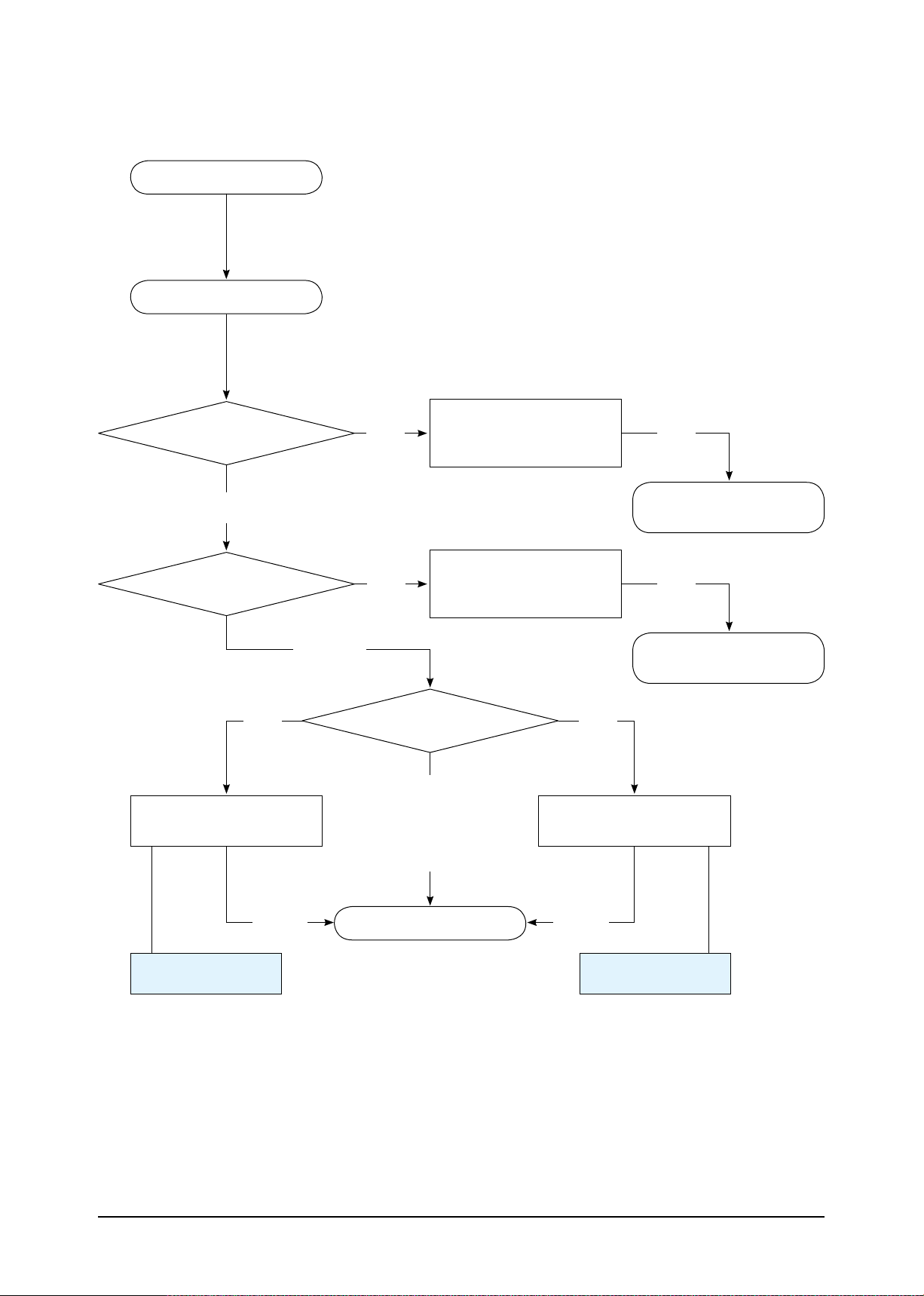
4-1-4 No HDMI Video Output
No HDMI Video Output
Check the HDMI signal
Output.
Check the outputs of
the pin 33, 34, 35, 36, 37, 38,
39, 40, 89, 90, 91, 92 and
HD_CLK 131 of
MIC1 ES8391.
Yes
Check the outputs of the
pin 26, 27, 29, 30, 32, 33, 35, 36
of HIC1 ES7108S.
Yes
Check the HCN1 Output.
Refer to wave pattern
image of Fig. 4-6.
Refer to wave pattern
image of Fig. 4-7.
No
No
Check if VDD of
3.3V is measured at the pin 1, 14 and
58 of MIC1.
Yes
Replace the MIC1 IC.
Check if the
VDD 3.3V of HIC1 is measured
at the pin of 13, 28, 34, 48 and 71.
Check if the VDD 1.8V of HIC1 is
measured at the pin of 16,
45, 59 and 74.
Yes
Replace the HIC1 IC.
No
Check if the pin 3, 4, 5 of CN2
is 3.3V.
No
Check the REG1 output
pin 2 for VDD1.8V and REG2
output pin 2 for 3.3V.
Replace the jack.
Page 37
Samsung Electronics 4-15
Troubleshooting
RIC4
RIC1
MIC1
DIC1
DIC2
CN09
1
MAIN_MPEG Page, 7-15
1
1
MAIN PCB Top Page, 6-19
<Fig. 4-6>
Page 38
4-16 Samsung Electronics
Troubleshooting
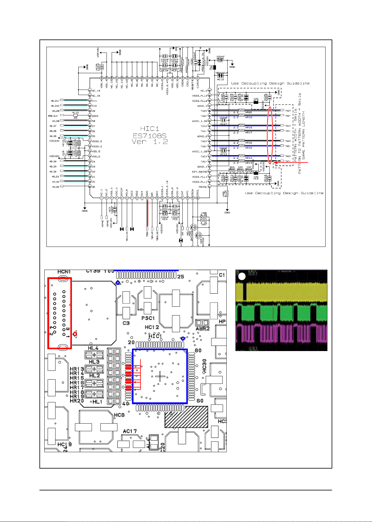
HIC1
MIC1
U1
DIC1
HCN1
2
MAIN_HDMI Page, 7-11
2
2
MAIN PCB Top Page, 6-19
<Fig. 4-7>
Page 39
Samsung Electronics 4-17
Troubleshooting
4-1-5 DECK Failure
Power On
Disc Insert
Does disc spin stuck?
No,
Spin OK
How about
Pickup Power?
CD DVD
Check CD Signal
(RCN1 7P CD/DVD)
OK,
No Problem
How about Pickup Power?
Yes,
Stuck
NG
Disc Inserted
But
NO DISC
DISC ERROR
Please check
Main PCB and Deck 24pin
connection.
Check RCN1 RF50V 14P, 21P:
4.8V~5.2V and MVREF 21P:
2V~2.1V
Check DVD Signal
(RCN1 7P CD/DVD)
or
NG
Reassemble
Main PCB and DECK
NG
Reassemble
Main PCB and DECK
Not Like
This
Refer to wave pattern
image of Fig. 4-8.
Change DECK
Not Like
This
Refer to wave pattern
image of Fig. 4-8.
Page 40

4-18 Samsung Electronics
Troubleshooting
CN7
CN11
RCN3
RCN2
CN5
RCN1
Check CD Signal
1
Check DVD Signal
2
1
Check CD Signal
MAIN_MPEG Page, 7-15
Power On
Position
Check DVD Signal
2
Power On
Position
Low
Active
High
Active
1
2
MAIN PCB Bottom Page, 6-21
<Fig. 4-8>
Page 41

Samsung Electronics 4-19
Troubleshooting
4-2 Measures to be taken when the Protection Circuit operates
4-2-1 In case of power protection
The Condition of Power Protection Active.
1. Voltage of SMPS’s PVDD (+35V, CN2) is higher or lower than Standards.
Normal Condition Voltage Range: PVDD (+35V, J3): about +35V
2. Over-current occurs to AMP IC. (Over-output or Output short)
3. AMP IC’s temperature exceeds 150°C.
4. No supply voltage on GATE DRIVER.
Part
Location
Pin No.
+8V
+5V
CN3
+3.3V
SMPS
+5.6V
+42V
PVDD (about 35V)
CN2
-12V
+12V
<Table 4-1>
4-2-2 Amp Power Stage TAS5142
1. OTW: Active, IC’s inner temperature exceeds over 150°C.
(Under 2.7V, Protection Circuit wills Active)
Protection Circuit Operation
Open Short
X
X
X X
X X
X X
-
X X
X
Remark
2. TAS5142 3
TH
PIN: Shout down
1
2
(Under 2.7V, Protection Circuit wills Active)
<Fig. 4-9>
Page 42
4-20 Samsung Electronics
Troubleshooting
4-2-3 AMP Pre-inspection
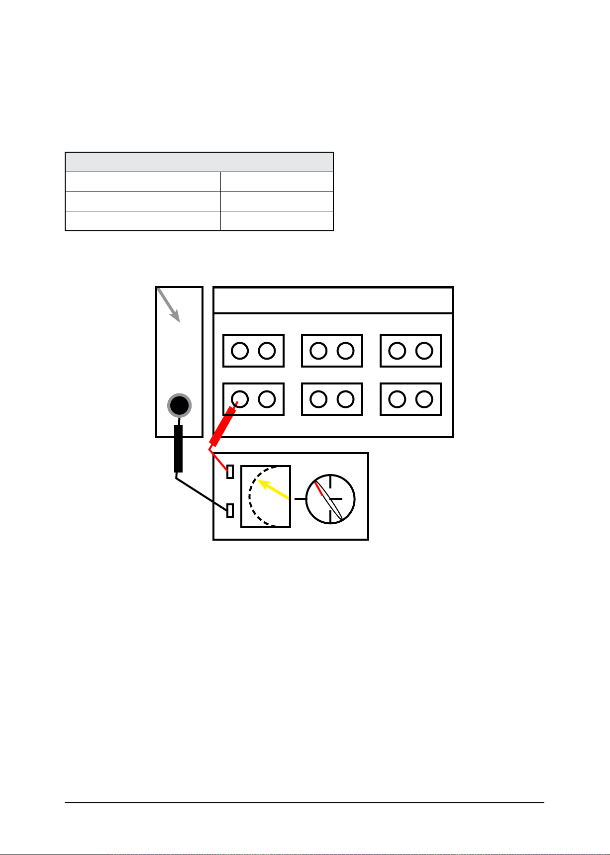
You can check AMP Malfunction before disassembling Main Unit. (Do not Insert AC-Cord in AC-Socket)
Resistance in using Tester
F/R CH 10kΩ
CENTER 10kΩ
SUBWOOFER 10kΩ
<Table 4-2>
If Measured Resistance is very different from above numbers. There is a Problem. → AMP PCB Problem
5.1CH SPEAKER OUTPUT
FRONT R CENTER FRONT L
GND
REAR R REAR L
SUBWOOFER
Page 43

Samsung Electronics 4-21
Troubleshooting
4-3 Initialization & Upgrade Methods
4-3-1 MICOM Initialization & Update
MICOM Initial
In STANDBY condition, press “STOP” button of Main Unit more than 5 seconds, STANDBY RED LED will turn off
and turn on again. Then Initialization complete.
MICOM Update
1. At Bottom side of Main Unit, Connecting 6 pin cable.
2. Wire to Update connector-look like an oval hole then update
start.
Required Equipment:
Computer, Rom Writer, Connecting Cable, Update Program.
Update is available Only OTP type MICOM.
<Fig. 4-10 Connecting 6 Pin>
<Fig. 4-11 Connecting Rom writer>
<Fig. 4-12 Update Program>
Page 44

4-22 Samsung Electronics
Troubleshooting
4-3-2 DVD flash Initialization & Update
Checking out MICOM & MPEG flash Version
1. Play DVD-DISC or CD-DISC.
2. Open DISC-TRAY, Press "MENU" button on the Remote
Control.
3. Press "8", "9", "5" one by one, then MPEG version will be
displayed on the screen and MICOM version on the front
display.
<Fig. 4-13 MPEG Flash Version>
<Fig. 4-14 MICOM Version>
Page 45

Samsung Electronics 4-23
Troubleshooting
DVD flash Initialization & Update (firmware)
1. Prepare or Making CD/DVD or USB that contains HEX file for
Update.
2. Select the folder which has update file, then ‘Updating’ will
appear on the screen.
After completing the update, the power will go out and on, then
tray will open automatically.
3. Make the unit ‘NO DISC’ state if there is a disc and then close
the tray.
4. Press "STOP" button of Main Unit 5 seconds more, Display
Indicator shows ‘INITIALIZE’ then Power go out.
<Fig. 4-15 Connecting USB>
5. Initialization complete.
<Fig. 4-16 TV Display (On Updating)>
<Fig. 4-17 Update Start>
Page 46

MEMO
4-24 Samsung Electronics
Page 47

Exploded View & Part List
5. Exploded View & Part List
5-1 SET Exploded View ..............................................................................5-2
5-2 Speaker System
5-3 Electrical Part List ................................................................................
....................................................................................5-4
5-5
Samsung Electronics 5-1
This Document can not be used without Samsung’s authorization.
Page 48

Exploded View & Part List
AC010
AS078
AL094
SHEET
AA400
AS198
AA390
AS109
AC169
AM020
AS111
AD285
AD520
AD090
AK170
AK270
AC050
AK290
AS222
5-1 SET Exploded View
5-2 Samsung Electronics
This Document can not be used without Samsung’s authorization.
Page 49

Exploded View & Part List
Part List
Loc. No. Code No. Description;Specification Q’ty SNA Remark
AA390 AH81-04174A A/S PART-USB;HT-A100,-,-,-,-,-,- 1 SA
AA400 AH81-04173A A/S PART-VFD;HT-A100,-,-,-,-,-,- 1 SA
AC010 AH64-04491B CABINET-FRONT;HT-A100,ABS+PMMA,-,-,-,-,B 1 SA
AC050 AH64-04490C CABINET-REAR;HT-A100,ABS+PMMA,-,-,-,-,BL 1 SNA
AC169 AH63-01546A COVER-AC CORD;HT-A100,ABS,T2.5,W24.2,L20 1 SA
AD090 AH64-04492A DECORATION-CD;HT-A100,ABS,T1.6,W8.2,L149 1 SNA
AD285 AH64-04493A DECORATION-REAR;HT-A100,ABS,T2.5,W97.5,L 1 SNA
AD520 AH64-04494A DOOR-USB;HT-A100,ABS,T3.5,-,W12.4,L84.5 1 SA
AK170 AH64-04497A KNOB-FUNCTION;HT-A100,ABS+PC,T1.5,W16.3, 1 SA
AK270 AH64-04495A KNOB-OPEN;HT-A100,ABS,T1.5,W17.55,L15.87 1 SA
AK290 AH64-04496A KNOB-POWER;HT-A100,ABS+PC,T1.5,W17.3,L19 1 SA
AL094 AH67-00478A LENS-LIGHTING;HT-TX500,PMMA,ice blue,-,- 1 SA
AM020 AH31-00029E MOTOR FAN;C161NK10B0110,MX-GT88,0.15A,-, 1 SA
AS078 AH63-01636A SHEET-FRONT;HT-A100,PC,T0.2,W30,L50,BLK, 1 SNA
AS109 AH63-01596A SHEET-SIDE;HT-A100,PC,T0.5,W32,L158,-,- 1 SNA
AS111 AH63-01549B SHEET-REAR;HT-A100/EXP,TETRON,0.3T,-,-,B 1 SNA
AS198 AH63-01548A SHIELD-FRONT;HT-A100,SECC,T0.8,W169.4,L4 1 SNA
AS222 AH63-01547A SHIELD-REAR;HT-A100,SECC,T0.8,W440,L177, 1 SNA
SHEET AH63-01558A SHEET-FILTER;HT-A100,PC,T0.3,W36,L126,-, 1 SNA
MECHA AH59-01773A DECK-MECHA DVD;VSH-L33D-0826,-,MAGNET,31 1 SA
PCB-AMP AH92-02863D ASSY PCB AMP-EUROPE;-,HT-A100 AMP ASS,EX 1 SA
PCB-KEY AH92-02831A ASSY PCB KEY;-,HT-XA100 KEY PC,EXPOXY 2L 1 SA
PCB-MAIN AH92-02862D ASSY PCB MAIN;-,HT-A100 MAIN PC,EXPOXY 4 1 SA
PCB-POWER AH92-02866A ASSY PCB POWER-KEY;-,HT-A100 POWER K,EXP 1 SA
PCB-SMPS AH44-00174A SMPS;HT-A100,ORTP-688,QRC,-,110V~22 1 SA
POWER-CORD
TUNER-PACK AH40-00108A TUNER-PACK;KST-ML004FA0-H53,HT-P1200,FM, 1 SA
A 6003-001375 SCREW-TAPTITE;BH,+,-,B,M3,L8,ZPC(WHT),SW 11 SNA
B 6003-001464 SCREW-TAPTITE;BH,+,B,M3,L10,ZPC(WHT) 25 SNA
C 6003-000275 SCREW-TAPTITE;BH,+,-,B,M3,L10,ZPC(BLK),S 8 SA
Samsung Electronics 5-3
AH39-00257A CBF-POWER CORD;Z-88,-,CP2,250V,2.5A,1830 1 SA
This Document can not be used without Samsung’s authorization.
Page 50

Exploded View & Part List
Front Speaker (R)
Subwoofer
Front
Speaker (L)
5-2 Speaker System
Part List
Loc. No. Code No. Description;Specification Q’ty SNA Remark
Front Speaker
(R/L)
Subwoofer AH81-04167A
Speaker Wire AH81-02183E
AH81-04166A
AUDIO-RECEIVER;PS-A100,FRONT SPEAKER
SYSTEM,A/S PART,-,-,-,-
AUDIO-RECEIVER;PS-WA100,FOR PS-
A100,SUBWOOFER SPEAKER,-,-,-,-
SPEAKER-CORD ASS’Y;PS-Q100,SPK CORD
ASS’Y,Only for 2.1CH,-,-,-,-
2 SA
1 SA
1 SA
5-4 Samsung Electronics
This Document can not be used without Samsung’s authorization.
Page 51

Exploded View & Part List
5-3 Electrical Part List
Loc. No. Part No. Description;Specification Q’ty SNA Remark Loc. No. Part No. Description;Specification Q’ty SNA Remark
AH59-01913B SPEAKER SYSTEM-SATELLITE;PS-A100,XE 1 SA
AH81-02183E SPEAKER-CORD ASS’Y;PS-Q100,SPK CORD 1 SA
AH81-04123A AUDIO-RECEIVER-SPEAKER;CUSHION SATE 1 SNA
AH81-04166A AUDIO-RECEIVER;PS-A100,FRONT SPEAKE 2 SNA
AH81-03708A SPEAKER-REAR CASE;REAR CASE,-,-,-,- 1 SNA
AH81-03709A SPEAKER-FRONT PANEL;PS-A100,FRONT P 1 SNA
AH81-03710A SPEAKER-DECO;PS-A100,DECO,-,-,-,-,- 1 SNA
AH81-03723A SPEAKER-NET FRAME;PS-A100,NET FRAME 1 SNA
AH81-03725A SPEAKER-FRONT SPK;PS-A100,TWEETER_C 1 SNA
AH81-03816A SPEAKER-FRONT;PS-A100,PUNCHING GRIL 1 SNA
AH81-03817A SPEAKER-FRONT;PS-A100,PUNCHING GRIL 1 SNA
AH81-04118A AUDIO-RECEIVER-SPEAKER;FRONT UNIT, 1 SNA
AH81-04121A AUDIO-RECEIVER-SPEAKER;TWEETER,FOR 1 SNA
AH81-04122A AUDIO-RECEIVER-SPEAKER;NETWORK FRON 1 SNA
AH59-01914B SPEAKER SYSTEM;PS-A100,XEU,SUBWOOFE 1 SA
AH81-02492C SPEAKER;CUSHION-SUBW/F,,BOTTOM,FOR 1 SNA
AH81-02492D SPEAKER;CUSHION-SUBW/F,TOP,FOR PS-X 1 SNA
AH81-04167A AUDIO-RECEIVER;PS-WA100,FOR PS-A100 1 SNA
AH81-00830B A/S PART-NET FRAME;PS WA150,-,-,NET 1 SNA
AH81-01584G A/S PART-DUCT;PSWS665T,-,DUCT,RRSS, 1 SNA
AH81-02401A A/S PART;FRONT PANEL-SUBWOOFER,FOR 1 SNA
AH81-02402A A/S PART;TOP PANEL-SUBWOOFER,FOR PS 1 SNA
AH81-02403A A/S PART;NET FRAME-SUBWOOFER,FOR PS 1 SNA
AH81-02417A A/S PART;FOOT-SUBWOOFER,FOR PS-X250 1 SNA
AH81-02687A A/S PART-SUBWOOFER UNIT;PS-X250,SUB 1 SA
AH97-02612F ASSY-MAIN OTHER;HT-XA100/XEO,-,-,- 1 SNA
AH63-01301A SHEET-SET;HT-Q40,-,-,-,-,-,- 1 SNA
AH68-00371A LABEL-BAR CODE;DVD-611/XAA,-,MOJO20 1.05 SNA
AH68-01984A MANUAL-CLEANING;HT-X200,-,-,-,ART P 1 SNA
AH68-02045A LABEL-POP LABEL;HT-A100,EXP,RAINBOW 1 SNA
AH68-02078B LABEL RATING;HT-A100,XEF,SLIVER PET 1.05 SNA
AH69-02183A CUSHION-TOP;HT-A100,EPS,T30mm,-,-,- 1 SNA
AH69-02184A CUSHION-BOTTOM;HT-A100,EPS,T30mm,-, 1 SNA
AH97-02614F ASSY ACCESSORY;HT-XA100/XER,-,-,- 1 SNA
4301-000116 BATTERY-ALKALINE;9V,-,-,17.5x26.5x4 2 SA
6902-000385 BAG PE;LDPE,T0.03,W250,L350,TRP,8,1 1 SNA
AH68-00650L MARK RECYCLE;YP-P2,ELS,ENG,-,MOJO40 1 SA
AH68-02056D MANUAL USERS;HT-A100,XET,ITA/SPN/PO 1 SA
AH68-50254B LABEL-SERIAL;ART PAPER,T0.1,L10,W45 1.05 SNA
AH81-02286C A/S-EYEGLASS CLOTH;HT-TXQ120,POLY-B 1 SNA
FR1 2007-000081 R-CHIP;2.7Kohm,5%,1/10W,TP,1608 1 SA
FR10 2007-000124 R-CHIP;2.2Kohm,5%,1/10W,TP,1608 1 SA
FR11 2007-000079 R-CHIP;1.8Kohm,5%,1/10W,TP,1608 1 SA
FR12 2007-000123 R-CHIP;1.5Kohm,5%,1/10W,TP,1608 1 SA
FR13 2007-000081 R-CHIP;2.7Kohm,5%,1/10W,TP,1608 1 SA
FR14 2007-000081 R-CHIP;2.7Kohm,5%,1/10W,TP,1608 1 SA
FR15 2007-000081 R-CHIP;2.7Kohm,5%,1/10W,TP,1608 1 SA
FR16 2007-000078 R-CHIP;1Kohm,5%,1/10W,TP,1608 1 SA
FR17 2007-000122 R-CHIP;1.2Kohm,5%,1/10W,TP,1608 1 SA
FR18 2007-000107 R-CHIP;470Kohm,5%,1/10W,TP,1608 1 SA
FR19 2007-000107 R-CHIP;470Kohm,5%,1/10W,TP,1608 1 SA
FR2 2007-000107 R-CHIP;470Kohm,5%,1/10W,TP,1608 1 SA
FR20 2007-000081 R-CHIP;2.7Kohm,5%,1/10W,TP,1608 1 SA
FR21 2007-000081 R-CHIP;2.7Kohm,5%,1/10W,TP,1608 1 SA
FR22 2007-000081 R-CHIP;2.7Kohm,5%,1/10W,TP,1608 1 SA
FR23 2007-000081 R-CHIP;2.7Kohm,5%,1/10W,TP,1608 1 SA
FR3 2007-000084 R-CHIP;4.7Kohm,5%,1/10W,TP,1608 1 SA
FR4 2007-000107 R-CHIP;470Kohm,5%,1/10W,TP,1608 1 SA
FR5 2007-000081 R-CHIP;2.7Kohm,5%,1/10W,TP,1608 1 SA
FR6 2007-000107 R-CHIP;470Kohm,5%,1/10W,TP,1608 1 SA
FR7 2007-000107 R-CHIP;470Kohm,5%,1/10W,TP,1608 1 SA
FR8 2007-000107 R-CHIP;470Kohm,5%,1/10W,TP,1608 1 SA
FR9 2007-000107 R-CHIP;470Kohm,5%,1/10W,TP,1608 1 SA
FWN1 AH39-00985A WIRE HARNESS-OPEN KEY-MAIN;HT-XA100 1 SNA
FZD1 0403-001064 DIODE-ZENER;RLZ5.1B,4.94-5.2V,500mW 1 SA
FZD2 0403-001064 DIODE-ZENER;RLZ5.1B,4.94-5.2V,500mW 1 SA
FZD3 0403-001064 DIODE-ZENER;RLZ5.1B,4.94-5.2V,500mW 1 SA
FZD4 0403-001064 DIODE-ZENER;RLZ5.1B,4.94-5.2V,500mW 1 SA
FZD5 0403-001064 DIODE-ZENER;RLZ5.1B,4.94-5.2V,500mW 1 SA
FZD6 0403-001064 DIODE-ZENER;RLZ5.1B,4.94-5.2V,500mW 1 SA
FZD7 0403-001064 DIODE-ZENER;RLZ5.1B,4.94-5.2V,500mW 1 SA
FZD8 0403-001064 DIODE-ZENER;RLZ5.1B,4.94-5.2V,500mW 1 SA
TP10 1209-001742 IC-SENSOR;SS02,SOT26,6P,2.9x1.6mm,P 1 SA
TP11 1209-001742 IC-SENSOR;SS02,SOT26,6P,2.9x1.6mm,P 1 SA
TP12 1209-001742 IC-SENSOR;SS02,SOT26,6P,2.9x1.6mm,P 1 SA
TP14 1209-001742 IC-SENSOR;SS02,SOT26,6P,2.9x1.6mm,P 1 SA
TP17 1209-001742 IC-SENSOR;SS02,SOT26,6P,2.9x1.6mm,P 1 SA
TP4 1209-001742 IC-SENSOR;SS02,SOT26,6P,2.9x1.6mm,P 1 SA
TP5 1209-001742 IC-SENSOR;SS02,SOT26,6P,2.9x1.6mm,P 1 SA
TP6 1209-001742 IC-SENSOR;SS02,SOT26,6P,2.9x1.6mm,P 1 SA
XA100_KEY_PCB
AH41-01122A PCB-KEY;HT-XA100 KEY PCB,EPOXY,2,0, 0.143 SNA
3809-002095 CABLE-FLAT;30V,80,70mm,15P,1mm,UL20 1 SNA
3809-002096 CABLE-FLAT;30V,80,60mm,23P,1mm,UL20 1 SNA
3809-002097 CABLE-FLAT;30V,80,80,23P,1mm,UL2069 1 SNA
3809-002098 DR2DB2FLAT;30V,80,140mm,13P,1.25mm, 1 SA
AH92-02831A ASSY PCB KEY;-,HT-XA100 KEY PC,EXPO 1 SA
FC1 2203-000189 C-CER,CHIP;100nF,+80-20%,25V,Y5V,16 1 SA
FC10 2203-000189 C-CER,CHIP;100nF,+80-20%,25V,Y5V,16 1 SA
FC3 2203-005148 C-CER,CHIP;100nF,10%,16V,X7R,TP,160 1 SA
FC4 2203-000189 C-CER,CHIP;100nF,+80-20%,25V,Y5V,16 1 SA
FC5 2203-000189 C-CER,CHIP;100nF,+80-20%,25V,Y5V,16 1 SA
FC6 2203-000189 C-CER,CHIP;100nF,+80-20%,25V,Y5V,16 1 SA
FC7 2203-000189 C-CER,CHIP;100nF,+80-20%,25V,Y5V,16 1 SA
FC8 2203-000189 C-CER,CHIP;100nF,+80-20%,25V,Y5V,16 1 SA
FC9 2203-000189 C-CER,CHIP;100nF,+80-20%,25V,Y5V,16 1 SA
FCN1 AH39-00983A WIRE HARNESS-MAIN-FUNC.KEY;HT-XA100 1 SNA
Samsung Electronics 5-5
This Document can not be used without Samsung’s authorization.
3809-002099 CABLE-FLAT;30V,80,175mm,20P,1mm,UL2 1 SNA
AH39-00257A CBF-POWER CORD;Z-88,-,CP2,250V,2.5A 1 SA
AH40-00108A TUNER-PACK;KST-ML004FA0-H53,HT-P120 1 SA
AH44-00174A SMPS;HT-A100,ORTP-688,QRC,-,110V~22 1 SA
AH59-01773A DECK-MECHA DVD;VSH-L33D-0826,-,MAGN 1 SA
AH81-04174A A/S PART-USB;HT-A100,-,-,-,-,-,- 1 SA
AH97-02705E ASSY REAR-KEY KITTING;HT-A100/XEE,- 1 SNA
AH99-10012A ASSY AUTO INSERT-PCB-KEY;-,HT-XA100 1 SNA
AH92-02862D ASSY PCB MAIN;-,HT-A100 MAIN PC,EXP 1 SA
AC10 2402-000130 C-AL,SMD;2.2uF,20%,50V,GP,TP,4.3x4. 1 SA
Page 52

Exploded View & Part List
Loc. No. Part No. Description;Specification Q’ty SNA Remark Loc. No. Part No. Description;Specification Q’ty SNA Remark
AC11 2203-005148 C-CER,CHIP;100nF,10%,16V,X7R,TP,160 1 SA
AC12 2203-005148 C-CER,CHIP;100nF,10%,16V,X7R,TP,160 1 SA
AC13 2402-000008 C-AL,SMD;47uF,20%,16V,GP,TP,6.6x6.6 1 SA
AC14 2402-000008 C-AL,SMD;47uF,20%,16V,GP,TP,6.6x6.6 1 SA
AC15 2203-000491 C-CER,CHIP;2.2nF,10%,50V,X7R,1608 1 SA
AC16 2203-000491 C-CER,CHIP;2.2nF,10%,50V,X7R,1608 1 SA
AC17 2402-001049 C-AL,SMD;10uF,20%,16V,GP,TP,3.3x3.3 1 SA
AC18 2203-005148 C-CER,CHIP;100nF,10%,16V,X7R,TP,160 1 SA
AC19 2402-001049 C-AL,SMD;10uF,20%,16V,GP,TP,3.3x3.3 1 SA
AC2 2402-000130 C-AL,SMD;2.2uF,20%,50V,GP,TP,4.3x4. 1 SA
AC20 2402-000008 C-AL,SMD;47uF,20%,16V,GP,TP,6.6x6.6 1 SA
AC21 2402-000008 C-AL,SMD;47uF,20%,16V,GP,TP,6.6x6.6 1 SA
AC22 2203-005148 C-CER,CHIP;100nF,10%,16V,X7R,TP,160 1 SA
AC25 2203-002398 C-CER,CHIP;22nF,10%,50V,X7R,1608 1 SA
AC26 2203-005148 C-CER,CHIP;100nF,10%,16V,X7R,TP,160 1 SA
AC27 2203-005148 C-CER,CHIP;100nF,10%,16V,X7R,TP,160 1 SA
AC28 2203-005148 C-CER,CHIP;100nF,10%,16V,X7R,TP,160 1 SA
AC29 2402-001042 C-AL,SMD;100uF,20%,16V,GP,TP,6.6x6. 1 SA
AC3 2402-000130 C-AL,SMD;2.2uF,20%,50V,GP,TP,4.3x4. 1 SA
AC30 2203-005148 C-CER,CHIP;100nF,10%,16V,X7R,TP,160 1 SA
AC31 2203-005148 C-CER,CHIP;100nF,10%,16V,X7R,TP,160 1 SA
AC32 2402-001049 C-AL,SMD;10uF,20%,16V,GP,TP,3.3x3.3 1 SA
AC33 2402-001049 C-AL,SMD;10uF,20%,16V,GP,TP,3.3x3.3 1 SA
AC34 2203-005148 C-CER,CHIP;100nF,10%,16V,X7R,TP,160 1 SA
AC7 2402-000130 C-AL,SMD;2.2uF,20%,50V,GP,TP,4.3x4. 1 SA
AC8 2402-000130 C-AL,SMD;2.2uF,20%,50V,GP,TP,4.3x4. 1 SA
AC9 2402-000130 C-AL,SMD;2.2uF,20%,50V,GP,TP,4.3x4. 1 SA
ACN10 3708-002403 CONNECTOR-FPC/FFC/PIC;23P,1mm,SMD-S 1 SA
AD7 3301-001495 BEAD-SMD;120ohm,2012,2500mA,TP,115o 1 SA
AIC1 1002-001548 IC-A/D CONVERTER;CS5345,24,LQFP,48P 1 SA
AL1 3301-001495 BEAD-SMD;120ohm,2012,2500mA,TP,115o 1 SA
AL2 3301-001495 BEAD-SMD;120ohm,2012,2500mA,TP,115o 1 SA
AL3 3301-001495 BEAD-SMD;120ohm,2012,2500mA,TP,115o 1 SA
AL4 3301-001495 BEAD-SMD;120ohm,2012,2500mA,TP,115o 1 SA
AL6 3301-001495 BEAD-SMD;120ohm,2012,2500mA,TP,115o 1 SA
AMR1 2007-000309 R-CHIP;10ohm,5%,1/10W,TP,1608 1 SA
AMR10 2007-000052 R-CHIP;10Kohm,1%,1/10W,TP,1608 1 SA
AMR11 2007-000052 R-CHIP;10Kohm,1%,1/10W,TP,1608 1 SA
AMR12 2007-000072 R-CHIP;47ohm,5%,1/10W,TP,1608 1 SA
AMR13 2007-000052 R-CHIP;10Kohm,1%,1/10W,TP,1608 1 SA
AMR14 2007-000113 R-CHIP;33ohm,5%,1/10W,TP,1608 1 SA
AMR15 2007-000097 R-CHIP;47Kohm,5%,1/10W,TP,1608 1 SA
AMR16 2007-000052 R-CHIP;10Kohm,1%,1/10W,TP,1608 1 SA
AMR17 2007-000113 R-CHIP;33ohm,5%,1/10W,TP,1608 1 SA
AMR18 2007-000097 R-CHIP;47Kohm,5%,1/10W,TP,1608 1 SA
AMR19 2007-000097 R-CHIP;47Kohm,5%,1/10W,TP,1608 1 SA
AMR2 2007-000309 R-CHIP;10ohm,5%,1/10W,TP,1608 1 SA
AMR20 2007-000070 R-CHIP;0ohm,5%,1/10W,TP,1608 1 SA
AMR21 2007-000070 R-CHIP;0ohm,5%,1/10W,TP,1608 1 SA
AMR22 2007-000072 R-CHIP;47ohm,5%,1/10W,TP,1608 1 SA
AMR23 2007-000052 R-CHIP;10Kohm,1%,1/10W,TP,1608 1 SA
AMR24 2007-000052 R-CHIP;10Kohm,1%,1/10W,TP,1608 1 SA
AMR25 2007-000097 R-CHIP;47Kohm,5%,1/10W,TP,1608 1 SA
AMR26 2007-000094 R-CHIP;22Kohm,5%,1/10W,TP,1608 1 SA
AMR27 2007-000094 R-CHIP;22Kohm,5%,1/10W,TP,1608 1 SA
AMR28 2007-000052 R-CHIP;10Kohm,1%,1/10W,TP,1608 1 SA
AMR29 2007-000052 R-CHIP;10Kohm,1%,1/10W,TP,1608 1 SA
AMR3 2007-000072 R-CHIP;47ohm,5%,1/10W,TP,1608 1 SA
AMR30 2007-002425 R-CHIP;1ohm,5%,1/10W,TP,1608 1 SA
AMR31 2007-000052 R-CHIP;10Kohm,1%,1/10W,TP,1608 1 SA
AMR32 2007-000094 R-CHIP;22Kohm,5%,1/10W,TP,1608 1 SA
AMR33 2007-000116 R-CHIP;120ohm,5%,1/10W,TP,1608 1 SA
AMR34 2007-000072 R-CHIP;47ohm,5%,1/10W,TP,1608 1 SA
AMR35 2007-000109 R-CHIP;1Mohm,5%,1/10W,TP,1608 1 SA
AMR36 2007-000113 R-CHIP;33ohm,5%,1/10W,TP,1608 1 SA
AMR37 2007-000094 R-CHIP;22Kohm,5%,1/10W,TP,1608 1 SA
AMR38 2007-000074 R-CHIP;100ohm,5%,1/10W,TP,1608 1 SA
AMR39 2007-000074 R-CHIP;100ohm,5%,1/10W,TP,1608 1 SA
AMR4 2007-000072 R-CHIP;47ohm,5%,1/10W,TP,1608 1 SA
AMR40 2007-000074 R-CHIP;100ohm,5%,1/10W,TP,1608 1 SA
AMR41 2007-000074 R-CHIP;100ohm,5%,1/10W,TP,1608 1 SA
AMR47 2007-000072 R-CHIP;47ohm,5%,1/10W,TP,1608 1 SA
AMR48 2007-000072 R-CHIP;47ohm,5%,1/10W,TP,1608 1 SA
AMR49 2007-000072 R-CHIP;47ohm,5%,1/10W,TP,1608 1 SA
AMR5 2007-000072 R-CHIP;47ohm,5%,1/10W,TP,1608 1 SA
AMR50 2007-000072 R-CHIP;47ohm,5%,1/10W,TP,1608 1 SA
AMR53 2007-000072 R-CHIP;47ohm,5%,1/10W,TP,1608 1 SA
AMR6 2007-000072 R-CHIP;47ohm,5%,1/10W,TP,1608 1 SA
AMR7 2007-000052 R-CHIP;10Kohm,1%,1/10W,TP,1608 1 SA
AMR8 2007-000052 R-CHIP;10Kohm,1%,1/10W,TP,1608 1 SA
AMR9 2007-000052 R-CHIP;10Kohm,1%,1/10W,TP,1608 1 SA
AR1 2007-000086 R-CHIP;5.6Kohm,5%,1/10W,TP,1608 1 SA
AR19 2007-000074 R-CHIP;100ohm,5%,1/10W,TP,1608 1 SA
AR2 2007-000102 R-CHIP;100Kohm,5%,1/10W,TP,1608 1 SA
AR24 2007-000074 R-CHIP;100ohm,5%,1/10W,TP,1608 1 SA
AR25 2007-000074 R-CHIP;100ohm,5%,1/10W,TP,1608 1 SA
AR28 2007-000076 R-CHIP;330ohm,5%,1/10W,TP,1608 1 SA
AR3 2007-000102 R-CHIP;100Kohm,5%,1/10W,TP,1608 1 SA
AR30 2007-000074 R-CHIP;100ohm,5%,1/10W,TP,1608 1 SA
AR31 2007-000074 R-CHIP;100ohm,5%,1/10W,TP,1608 1 SA
AR32 2007-000078 R-CHIP;1Kohm,5%,1/10W,TP,1608 1 SA
AR37 2007-000074 R-CHIP;100ohm,5%,1/10W,TP,1608 1 SA
AR38 2007-000074 R-CHIP;100ohm,5%,1/10W,TP,1608 1 SA
AR39 2007-000074 R-CHIP;100ohm,5%,1/10W,TP,1608 1 SA
AR4 2007-000086 R-CHIP;5.6Kohm,5%,1/10W,TP,1608 1 SA
AVC01 2402-001049 C-AL,SMD;10uF,20%,16V,GP,TP,3.3x3.3 1 SA
AVC02 2203-005148 C-CER,CHIP;100nF,10%,16V,X7R,TP,160 1 SA
AVC03 2203-005819 C-CER,CHIP;1000nF,+80-20%,16V,Y5V,- 1 SA
AVC04 2402-001049 C-AL,SMD;10uF,20%,16V,GP,TP,3.3x3.3 1 SA
AVC05 2203-005819 C-CER,CHIP;1000nF,+80-20%,16V,Y5V,- 1 SA
AVC06 2203-005819 C-CER,CHIP;1000nF,+80-20%,16V,Y5V,- 1 SA
AVC07 2203-005819 C-CER,CHIP;1000nF,+80-20%,16V,Y5V,- 1 SA
AVC08 2203-005148 C-CER,CHIP;100nF,10%,16V,X7R,TP,160 1 SA
AVC09 2203-005148 C-CER,CHIP;100nF,10%,16V,X7R,TP,160 1 SA
AVC10 2402-001042 C-AL,SMD;100uF,20%,16V,GP,TP,6.6x6. 1 SA
AVC11 2402-001042 C-AL,SMD;100uF,20%,16V,GP,TP,6.6x6. 1 SA
AVC12 2402-001042 C-AL,SMD;100uF,20%,16V,GP,TP,6.6x6. 1 SA
AVC13 2402-001042 C-AL,SMD;100uF,20%,16V,GP,TP,6.6x6. 1 SA
AVC14 2203-000280 C-CER,CHIP;0.01nF,0.5pF,50V,C0G,160 1 SA
AVC15 2203-000280 C-CER,CHIP;0.01nF,0.5pF,50V,C0G,160 1 SA
AVC16 2203-000280 C-CER,CHIP;0.01nF,0.5pF,50V,C0G,160 1 SA
AVC17 2203-000280 C-CER,CHIP;0.01nF,0.5pF,50V,C0G,160 1 SA
AVR01 2007-001167 R-CHIP;75ohm,5%,1/10W,TP,1608 1 SA
AVR02 2007-001167 R-CHIP;75ohm,5%,1/10W,TP,1608 1 SA
AVR03 2007-001167 R-CHIP;75ohm,5%,1/10W,TP,1608 1 SA
AVR04 2007-001167 R-CHIP;75ohm,5%,1/10W,TP,1608 1 SA
AVR05 2007-001167 R-CHIP;75ohm,5%,1/10W,TP,1608 1 SA
5-6 Samsung Electronics
This Document can not be used without Samsung’s authorization.
Page 53

Exploded View & Part List
Loc. No. Part No. Description;Specification Q’ty SNA Remark Loc. No. Part No. Description;Specification Q’ty SNA Remark
AVR06 2007-000125 R-CHIP;3.9Kohm,5%,1/10W,TP,1608 1 SA
AVR08 2007-001167 R-CHIP;75ohm,5%,1/10W,TP,1608 1 SA
AVR09 2007-001167 R-CHIP;75ohm,5%,1/10W,TP,1608 1 SA
AVR10 2007-001167 R-CHIP;75ohm,5%,1/10W,TP,1608 1 SA
AVR12 2007-000084 R-CHIP;4.7Kohm,5%,1/10W,TP,1608 1 SA
AVR13 2007-001167 R-CHIP;75ohm,5%,1/10W,TP,1608 1 SA
AVR14 2007-001167 R-CHIP;75ohm,5%,1/10W,TP,1608 1 SA
AVR15 2007-001167 R-CHIP;75ohm,5%,1/10W,TP,1608 1 SA
AVR16 2007-001167 R-CHIP;75ohm,5%,1/10W,TP,1608 1 SA
AVR54 2007-000072 R-CHIP;47ohm,5%,1/10W,TP,1608 1 SA
C100 2402-001059 C-AL,SMD;220##F,20%,6.3V,-,TP,6x6.6 1 SA
C101 2203-005249 C-CER,CHIP;100nF,10%,50V,X7R,1608 1 SA
C102 2203-005249 C-CER,CHIP;100nF,10%,50V,X7R,1608 1 SA
C103 2402-000167 C-AL,SMD;100uF,20%,10V,-,-,6.6x6.6x 1 SA
C139 2402-001049 C-AL,SMD;10uF,20%,16V,GP,TP,3.3x3.3 1 SA
C142 2203-000257 C-CER,CHIP;10nF,10%,50V,X7R,TP,1608 1 SA
C175 2203-005249 C-CER,CHIP;100nF,10%,50V,X7R,1608 1 SA
C176 2402-001059 C-AL,SMD;220##F,20%,6.3V,-,TP,6x6.6 1 SA
C180 2402-001059 C-AL,SMD;220##F,20%,6.3V,-,TP,6x6.6 1 SA
C181 2402-001059 C-AL,SMD;220##F,20%,6.3V,-,TP,6x6.6 1 SA
C182 2402-001059 C-AL,SMD;220##F,20%,6.3V,-,TP,6x6.6 1 SA
C183 2203-005249 C-CER,CHIP;100nF,10%,50V,X7R,1608 1 SA
C184 2203-005249 C-CER,CHIP;100nF,10%,50V,X7R,1608 1 SA
C185 2203-005249 C-CER,CHIP;100nF,10%,50V,X7R,1608 1 SA
C186 2203-005249 C-CER,CHIP;100nF,10%,50V,X7R,1608 1 SA
C187 2203-005249 C-CER,CHIP;100nF,10%,50V,X7R,1608 1 SA
C188 2203-005249 C-CER,CHIP;100nF,10%,50V,X7R,1608 1 SA
C189 2203-005249 C-CER,CHIP;100nF,10%,50V,X7R,1608 1 SA
C190 2203-005249 C-CER,CHIP;100nF,10%,50V,X7R,1608 1 SA
C191 2203-005249 C-CER,CHIP;100nF,10%,50V,X7R,1608 1 SA
C192 2203-005249 C-CER,CHIP;100nF,10%,50V,X7R,1608 1 SA
C193 2203-005249 C-CER,CHIP;100nF,10%,50V,X7R,1608 1 SA
C194 2203-005249 C-CER,CHIP;100nF,10%,50V,X7R,1608 1 SA
C195 2203-005249 C-CER,CHIP;100nF,10%,50V,X7R,1608 1 SA
C196 2203-005249 C-CER,CHIP;100nF,10%,50V,X7R,1608 1 SA
C197 2203-005249 C-CER,CHIP;100nF,10%,50V,X7R,1608 1 SA
C198 2203-005249 C-CER,CHIP;100nF,10%,50V,X7R,1608 1 SA
C20 2402-001059 C-AL,SMD;220##F,20%,6.3V,-,TP,6x6.6 1 SA
C3 2402-001049 C-AL,SMD;10uF,20%,16V,GP,TP,3.3x3.3 1 SA
C4 2203-005249 C-CER,CHIP;100nF,10%,50V,X7R,1608 1 SA
C5 2203-005249 C-CER,CHIP;100nF,10%,50V,X7R,1608 1 SA
CC1 2203-005148 C-CER,CHIP;100nF,10%,16V,X7R,TP,160 1 SA
CC2 2402-000167 C-AL,SMD;100uF,20%,10V,-,-,6.6x6.6x 1 SA
CC3 2203-005148 C-CER,CHIP;100nF,10%,16V,X7R,TP,160 1 SA
CC4 2203-005065 C-CER,CHIP;1000nF,+80-20%,10V,Y5V,1 1 SA
CC5 2402-000167 C-AL,SMD;100uF,20%,10V,-,-,6.6x6.6x 1 SA
CC6 2203-005148 C-CER,CHIP;100nF,10%,16V,X7R,TP,160 1 SA
CC7 2203-005148 C-CER,CHIP;100nF,10%,16V,X7R,TP,160 1 SA
CIC1 AK09-00159A IC MICOM;-,MC80C0316-MC015 D32,44,2 1 SA
CIC2 1103-001333 IC-EEPROM;24C08A,1Kx8Bit,SOP,8P,5x4 1 SA
CIC3 1203-002425 IC-POSI.FIXED REG.;1117,SOT-223,3P, 1 SA
CIC4 0505-001679 FET-SILICON;FDC6301N,N,25V,0.22A,5O 1 SA
CL1 3301-001495 BEAD-SMD;120ohm,2012,2500mA,TP,115o 1 SA
CL2 3301-001495 BEAD-SMD;120ohm,2012,2500mA,TP,115o 1 SA
CN1 3708-001958 CONNECTOR-FPC/FFC/PIC;13P,1.25MM,SM 1 SA
CN11 3708-001837 CONNECTOR-FPC/FFC/PIC;15P,1mm,SMD-S 1 SA
CN2 3708-002403 CONNECTOR-FPC/FFC/PIC;23P,1mm,SMD-S 1 SA
CN3 3708-001767 CONNECTOR-FPC/FFC/PIC;20P,1mm,SMD-S 1 SA
CN5 3711-003591 HEADER-BOARD TO CABLE;BOX,4P,1R,2mm 1 SA
CN6 3708-002023 CONNECTOR-FPC/FFC/PIC;6P,1MM,SMD-S, 1 SA
CN7 3711-003591 HEADER-BOARD TO CABLE;BOX,4P,1R,2mm 1 SA
CN8 3711-003591 HEADER-BOARD TO CABLE;BOX,4P,1R,2mm 1 SA
CN9 3711-003591 HEADER-BOARD TO CABLE;BOX,4P,1R,2mm 1 SA
CQ1 0501-000341 TR-SMALL SIGNAL;KSC1623-L,NPN,200mW 1 SA
CR1 2007-000070 R-CHIP;0ohm,5%,1/10W,TP,1608 1 SA
CR10 2007-000090 R-CHIP;10Kohm,5%,1/10W,TP,1608 1 SA
CR11 2007-000090 R-CHIP;10Kohm,5%,1/10W,TP,1608 1 SA
CR12 2007-000090 R-CHIP;10Kohm,5%,1/10W,TP,1608 1 SA
CR13 2007-000090 R-CHIP;10Kohm,5%,1/10W,TP,1608 1 SA
CR14 2007-000074 R-CHIP;100ohm,5%,1/10W,TP,1608 1 SA
CR15 2007-000074 R-CHIP;100ohm,5%,1/10W,TP,1608 1 SA
CR17 2007-000074 R-CHIP;100ohm,5%,1/10W,TP,1608 1 SA
CR2 2007-000071 R-CHIP;22ohm,5%,1/10W,TP,1608 1 SA
CR24 2007-000090 R-CHIP;10Kohm,5%,1/10W,TP,1608 1 SA
CR26 2007-000090 R-CHIP;10Kohm,5%,1/10W,TP,1608 1 SA
CR28 2007-000109 R-CHIP;1Mohm,5%,1/10W,TP,1608 1 SA
CR29 2007-000074 R-CHIP;100ohm,5%,1/10W,TP,1608 1 SA
CR3 2007-000071 R-CHIP;22ohm,5%,1/10W,TP,1608 1 SA
CR30 2007-000090 R-CHIP;10Kohm,5%,1/10W,TP,1608 1 SA
CR31 2007-000090 R-CHIP;10Kohm,5%,1/10W,TP,1608 1 SA
CR32 2007-000090 R-CHIP;10Kohm,5%,1/10W,TP,1608 1 SA
CR39 2007-000084 R-CHIP;4.7Kohm,5%,1/10W,TP,1608 1 SA
CR4 2007-000084 R-CHIP;4.7Kohm,5%,1/10W,TP,1608 1 SA
CR40 2007-000070 R-CHIP;0ohm,5%,1/10W,TP,1608 1 SA
CR41 2007-000070 R-CHIP;0ohm,5%,1/10W,TP,1608 1 SA
CR42 2007-000074 R-CHIP;100ohm,5%,1/10W,TP,1608 1 SA
CR43 2007-000090 R-CHIP;10Kohm,5%,1/10W,TP,1608 1 SA
CR44 2007-000078 R-CHIP;1Kohm,5%,1/10W,TP,1608 1 SA
CR45 2007-000081 R-CHIP;2.7Kohm,5%,1/10W,TP,1608 1 SA
CR46 2007-000093 R-CHIP;20Kohm,5%,1/10W,TP,1608 1 SA
CR47 2007-000074 R-CHIP;100ohm,5%,1/10W,TP,1608 1 SA
CR48 2007-000102 R-CHIP;100Kohm,5%,1/10W,TP,1608 1 SA
CR5 2007-000084 R-CHIP;4.7Kohm,5%,1/10W,TP,1608 1 SA
CR6 2007-000084 R-CHIP;4.7Kohm,5%,1/10W,TP,1608 1 SA
CR7 2007-000090 R-CHIP;10Kohm,5%,1/10W,TP,1608 1 SA
CR9 2007-000090 R-CHIP;10Kohm,5%,1/10W,TP,1608 1 SA
CSR1 2007-000084 R-CHIP;4.7Kohm,5%,1/10W,TP,1608 1 SA
CX1 2802-001165 RESONATOR-CERAMIC;4MHz,0.5%,TP,4.5x 1 SA
D4 0401-001099 DIODE-SWITCHING;1N4148WS,75V,150mA, 1 SA
DC1 2203-000189 C-CER,CHIP;100nF,+80-20%,25V,Y5V,16 1 SA
DC10 2203-000189 C-CER,CHIP;100nF,+80-20%,25V,Y5V,16 1 SA
DC11 2203-000189 C-CER,CHIP;100nF,+80-20%,25V,Y5V,16 1 SA
DC12 2203-000189 C-CER,CHIP;100nF,+80-20%,25V,Y5V,16 1 SA
DC18 2203-000815 C-CER,CHIP;0.033nF,5%,50V,C0G,1608 1 SA
DC19 2203-000815 C-CER,CHIP;0.033nF,5%,50V,C0G,1608 1 SA
DC3 2402-001049 C-AL,SMD;10uF,20%,16V,GP,TP,3.3x3.3 1 SA
DC4 2203-000189 C-CER,CHIP;100nF,+80-20%,25V,Y5V,16 1 SA
DC5 2203-000189 C-CER,CHIP;100nF,+80-20%,25V,Y5V,16 1 SA
DC6 2402-001049 C-AL,SMD;10uF,20%,16V,GP,TP,3.3x3.3 1 SA
DC7 2203-000189 C-CER,CHIP;100nF,+80-20%,25V,Y5V,16 1 SA
DC8 2402-001049 C-AL,SMD;10uF,20%,16V,GP,TP,3.3x3.3 1 SA
DC9 2203-000189 C-CER,CHIP;100nF,+80-20%,25V,Y5V,16 1 SA
DIC1 0904-002330 IC-DSP;CS48540,LQFP,48P,7x7mm,150MH 1 SA
DIC2 0802-001007 IC-CMOS LOGIC;74LCX244,BUFFER/LINE 1 SA
DIX1 2801-004021 CRYSTAL-SMD;24.576MHz,20ppm,28-AAN, 1 SA
DL1 3301-001495 BEAD-SMD;120ohm,2012,2500mA,TP,115o 1 SA
Samsung Electronics 5-7
This Document can not be used without Samsung’s authorization.
Page 54

Exploded View & Part List
Loc. No. Part No. Description;Specification Q’ty SNA Remark Loc. No. Part No. Description;Specification Q’ty SNA Remark
DL2 3301-001495 BEAD-SMD;120ohm,2012,2500mA,TP,115o 1 SA
DL3 3301-001495 BEAD-SMD;120ohm,2012,2500mA,TP,115o 1 SA
DR1 2007-000113 R-CHIP;33ohm,5%,1/10W,TP,1608 1 SA
DR10 2007-000082 R-CHIP;3.3Kohm,5%,1/10W,TP,1608 1 SA
DR11 2007-000113 R-CHIP;33ohm,5%,1/10W,TP,1608 1 SA
DR12 2007-000113 R-CHIP;33ohm,5%,1/10W,TP,1608 1 SA
DR13 2007-000082 R-CHIP;3.3Kohm,5%,1/10W,TP,1608 1 SA
DR14 2007-000070 R-CHIP;0ohm,5%,1/10W,TP,1608 1 SA
DR15 2007-000962 R-CHIP;5.1Kohm,1%,1/10W,TP,1608 1 SA
DR16 2007-000113 R-CHIP;33ohm,5%,1/10W,TP,1608 1 SA
DR17 2007-000113 R-CHIP;33ohm,5%,1/10W,TP,1608 1 SA
DR18 2007-000113 R-CHIP;33ohm,5%,1/10W,TP,1608 1 SA
DR19 2007-000113 R-CHIP;33ohm,5%,1/10W,TP,1608 1 SA
DR2 2007-000113 R-CHIP;33ohm,5%,1/10W,TP,1608 1 SA
DR20 2007-000113 R-CHIP;33ohm,5%,1/10W,TP,1608 1 SA
DR21 2007-000113 R-CHIP;33ohm,5%,1/10W,TP,1608 1 SA
DR22 2007-000113 R-CHIP;33ohm,5%,1/10W,TP,1608 1 SA
DR23 2007-000113 R-CHIP;33ohm,5%,1/10W,TP,1608 1 SA
DR24 2007-000113 R-CHIP;33ohm,5%,1/10W,TP,1608 1 SA
DR25 2007-000113 R-CHIP;33ohm,5%,1/10W,TP,1608 1 SA
DR26 2007-000113 R-CHIP;33ohm,5%,1/10W,TP,1608 1 SA
DR27 2007-000113 R-CHIP;33ohm,5%,1/10W,TP,1608 1 SA
DR3 2007-000113 R-CHIP;33ohm,5%,1/10W,TP,1608 1 SA
DR30 2007-000082 R-CHIP;3.3Kohm,5%,1/10W,TP,1608 1 SA
DR32 2007-000113 R-CHIP;33ohm,5%,1/10W,TP,1608 1 SA
DR35 2007-000113 R-CHIP;33ohm,5%,1/10W,TP,1608 1 SA
DR36 2007-000113 R-CHIP;33ohm,5%,1/10W,TP,1608 1 SA
DR37 2007-000090 R-CHIP;10Kohm,5%,1/10W,TP,1608 1 SA
DR38 2007-000475 R-CHIP;1Mohm,1%,1/10W,TP,1608 1 SA
DR39 2007-000082 R-CHIP;3.3Kohm,5%,1/10W,TP,1608 1 SA
DR4 2007-000113 R-CHIP;33ohm,5%,1/10W,TP,1608 1 SA
DR40 2007-000082 R-CHIP;3.3Kohm,5%,1/10W,TP,1608 1 SA
DR41 2007-000084 R-CHIP;4.7Kohm,5%,1/10W,TP,1608 1 SA
DR5 2007-000113 R-CHIP;33ohm,5%,1/10W,TP,1608 1 SA
DR6 2007-000113 R-CHIP;33ohm,5%,1/10W,TP,1608 1 SA
DR7 2007-000113 R-CHIP;33ohm,5%,1/10W,TP,1608 1 SA
DR8 2007-000113 R-CHIP;33ohm,5%,1/10W,TP,1608 1 SA
DR9 2007-000113 R-CHIP;33ohm,5%,1/10W,TP,1608 1 SA
ESD5 0406-001128 DIODE-TVS;MLVS-0603-E08,50V,-,- 1 SA
FB1 3301-001069 BEAD-SMD;120ohm,1.6x0.8x0.8mm,200mA 1 SA
FB2 3301-001069 BEAD-SMD;120ohm,1.6x0.8x0.8mm,200mA 1 SA
FB3 3301-001069 BEAD-SMD;120ohm,1.6x0.8x0.8mm,200mA 1 SA
FC1 2203-005148 C-CER,CHIP;100nF,10%,16V,X7R,TP,160 1 SA
FC6 2203-005148 C-CER,CHIP;100nF,10%,16V,X7R,TP,160 1 SA
FQ01 0504-000156 TR-DIGITAL;KSR2103,PNP,200MW,22K/22 1 SA
FR14 2007-000646 R-CHIP;270ohm,5%,1/4W,TP,3216 1 SA
HC1 2203-005148 C-CER,CHIP;100nF,10%,16V,X7R,TP,160 1 SA
HC10 2203-005148 C-CER,CHIP;100nF,10%,16V,X7R,TP,160 1 SA
HC11 2203-005148 C-CER,CHIP;100nF,10%,16V,X7R,TP,160 1 SA
HC12 2402-001059 C-AL,SMD;220##F,20%,6.3V,-,TP,6x6.6 1 SA
HC13 2203-005148 C-CER,CHIP;100nF,10%,16V,X7R,TP,160 1 SA
HC14 2203-005148 C-CER,CHIP;100nF,10%,16V,X7R,TP,160 1 SA
HC15 2402-001059 C-AL,SMD;220##F,20%,6.3V,-,TP,6x6.6 1 SA
HC16 2203-005148 C-CER,CHIP;100nF,10%,16V,X7R,TP,160 1 SA
HC17 2203-005148 C-CER,CHIP;100nF,10%,16V,X7R,TP,160 1 SA
HC18 2203-005065 C-CER,CHIP;1000nF,+80-20%,10V,Y5V,1 1 SA
HC19 2402-001059 C-AL,SMD;220##F,20%,6.3V,-,TP,6x6.6 1 SA
HC2 2203-005148 C-CER,CHIP;100nF,10%,16V,X7R,TP,160 1 SA
HC20 2203-005148 C-CER,CHIP;100nF,10%,16V,X7R,TP,160 1 SA
HC21 2203-005065 C-CER,CHIP;1000nF,+80-20%,10V,Y5V,1 1 SA
HC22 2203-005065 C-CER,CHIP;1000nF,+80-20%,10V,Y5V,1 1 SA
HC23 2203-005148 C-CER,CHIP;100nF,10%,16V,X7R,TP,160 1 SA
HC24 2402-001059 C-AL,SMD;220##F,20%,6.3V,-,TP,6x6.6 1 SA
HC25 2203-005148 C-CER,CHIP;100nF,10%,16V,X7R,TP,160 1 SA
HC26 2203-005148 C-CER,CHIP;100nF,10%,16V,X7R,TP,160 1 SA
HC27 2203-005148 C-CER,CHIP;100nF,10%,16V,X7R,TP,160 1 SA
HC28 2203-005148 C-CER,CHIP;100nF,10%,16V,X7R,TP,160 1 SA
HC29 2203-005148 C-CER,CHIP;100nF,10%,16V,X7R,TP,160 1 SA
HC3 2203-005148 C-CER,CHIP;100nF,10%,16V,X7R,TP,160 1 SA
HC30 2402-001059 C-AL,SMD;220##F,20%,6.3V,-,TP,6x6.6 1 SA
HC31 2402-001059 C-AL,SMD;220##F,20%,6.3V,-,TP,6x6.6 1 SA
HC32 2203-005148 C-CER,CHIP;100nF,10%,16V,X7R,TP,160 1 SA
HC35 2203-005148 C-CER,CHIP;100nF,10%,16V,X7R,TP,160 1 SA
HC36 2402-001049 C-AL,SMD;10uF,20%,16V,GP,TP,3.3x3.3 1 SA
HC37 2203-005148 C-CER,CHIP;100nF,10%,16V,X7R,TP,160 1 SA
HC39 2402-001042 C-AL,SMD;100uF,20%,16V,GP,TP,6.6x6. 1 SA
HC4 2203-005148 C-CER,CHIP;100nF,10%,16V,X7R,TP,160 1 SA
HC40 2203-005148 C-CER,CHIP;100nF,10%,16V,X7R,TP,160 1 SA
HC5 2203-005148 C-CER,CHIP;100nF,10%,16V,X7R,TP,160 1 SA
HC6 2203-005065 C-CER,CHIP;1000nF,+80-20%,10V,Y5V,1 1 SA
HC7 2203-005065 C-CER,CHIP;1000nF,+80-20%,10V,Y5V,1 1 SA
HC8 2402-001059 C-AL,SMD;220##F,20%,6.3V,-,TP,6x6.6 1 SA
HC9 2203-005148 C-CER,CHIP;100nF,10%,16V,X7R,TP,160 1 SA
HCN1 3701-001320 CONNECTOR-HDMI;19P,2R,FEMALE,DIP,AU 1 SA
HD2 0401-001090 DIODE-SWITCHING;1SS355,80V,100MA,SO 1 SA
HD3 0402-000309 DIODE-RECTIFIER;1SR154-400,400V,1A, 1 SA
HD4 0406-001128 DIODE-TVS;MLVS-0603-E08,50V,-,- 1 SA
HIC1 1205-003381 IC-TRANSMITTER;ES7108S,LQFP,80P,12x 1 SA
HIC3 1203-002935 IC-POSI.ADJUST REG.;AIC1117ACE,TO-2 1 SA
HL1 2901-001302 FILTER-EMI SMD;20V,0.3A,0pF,2.0x1.2 1 SA
HL10 3301-001495 BEAD-SMD;120ohm,2012,2500mA,TP,115o 1 SA
HL14 3301-001495 BEAD-SMD;120ohm,2012,2500mA,TP,115o 1 SA
HL15 3301-001069 BEAD-SMD;120ohm,1.6x0.8x0.8mm,200mA 1 SA
HL2 2901-001302 FILTER-EMI SMD;20V,0.3A,0pF,2.0x1.2 1 SA
HL3 2901-001302 FILTER-EMI SMD;20V,0.3A,0pF,2.0x1.2 1 SA
HL4 2901-001302 FILTER-EMI SMD;20V,0.3A,0pF,2.0x1.2 1 SA
HL5 3301-001495 BEAD-SMD;120ohm,2012,2500mA,TP,115o 1 SA
HL6 3301-001495 BEAD-SMD;120ohm,2012,2500mA,TP,115o 1 SA
HL7 3301-001495 BEAD-SMD;120ohm,2012,2500mA,TP,115o 1 SA
HL8 3301-001495 BEAD-SMD;120ohm,2012,2500mA,TP,115o 1 SA
HMQ1 0504-000156 TR-DIGITAL;KSR2103,PNP,200MW,22K/22 1 SA
HMQ2 0504-000128 TR-DIGITAL;-,NPN,200MW,22K/22K,SOT- 1 SA
HMQ3 0501-002184 TR-SMALL SIGNAL;KTD1304,NPN,200mW,S 1 SA
HMQ4 0501-002184 TR-SMALL SIGNAL;KTD1304,NPN,200mW,S 1 SA
HMR1 2007-000076 R-CHIP;330ohm,5%,1/10W,TP,1608 1 SA
HMR2 2007-000075 R-CHIP;220ohm,5%,1/10W,TP,1608 1 SA
HMR3 2007-000075 R-CHIP;220ohm,5%,1/10W,TP,1608 1 SA
HMR4 2007-000102 R-CHIP;100Kohm,5%,1/10W,TP,1608 1 SA
HMR5 2007-000102 R-CHIP;100Kohm,5%,1/10W,TP,1608 1 SA
HMR6 2007-000102 R-CHIP;100Kohm,5%,1/10W,TP,1608 1 SA
HPC1 2203-005148 C-CER,CHIP;100nF,10%,16V,X7R,TP,160 1 SA
HPC10 2402-000008 C-AL,SMD;47uF,20%,16V,GP,TP,6.6x6.6 1 SA
HPC11 2402-000008 C-AL,SMD;47uF,20%,16V,GP,TP,6.6x6.6 1 SA
HPC12 2203-000236 C-CER,CHIP;0.1nF,5%,50V,C0G,1608 1 SA
HPC13 2203-000236 C-CER,CHIP;0.1nF,5%,50V,C0G,1608 1 SA
HPC14 2402-001042 C-AL,SMD;100uF,20%,16V,GP,TP,6.6x6. 1 SA
HPC15 2402-001042 C-AL,SMD;100uF,20%,16V,GP,TP,6.6x6. 1 SA
5-8 Samsung Electronics
This Document can not be used without Samsung’s authorization.
Page 55

Exploded View & Part List
Loc. No. Part No. Description;Specification Q’ty SNA Remark Loc. No. Part No. Description;Specification Q’ty SNA Remark
HPC16 2203-000998 C-CER,CHIP;0.047nF,5%,50V,C0G,1608 1 SA
HPC17 2203-000998 C-CER,CHIP;0.047nF,5%,50V,C0G,1608 1 SA
HPC18 2203-000998 C-CER,CHIP;0.047nF,5%,50V,C0G,1608 1 SA
HPC2 2203-000531 C-CER,CHIP;2.7nF,10%,50V,X7R,1608 1 SA
HPC21 2203-000236 C-CER,CHIP;0.1nF,5%,50V,C0G,1608 1 SA
HPC22 2203-000236 C-CER,CHIP;0.1nF,5%,50V,C0G,1608 1 SA
HPC23 2203-000998 C-CER,CHIP;0.047nF,5%,50V,C0G,1608 1 SA
HPC26 2203-000236 C-CER,CHIP;0.1nF,5%,50V,C0G,1608 1 SA
HPC27 2203-000236 C-CER,CHIP;0.1nF,5%,50V,C0G,1608 1 SA
HPC28 2203-000236 C-CER,CHIP;0.1nF,5%,50V,C0G,1608 1 SA
HPC29 2203-000236 C-CER,CHIP;0.1nF,5%,50V,C0G,1608 1 SA
HPC3 2203-000236 C-CER,CHIP;0.1nF,5%,50V,C0G,1608 1 SA
HPC4 2203-000257 C-CER,CHIP;10nF,10%,50V,X7R,TP,1608 1 SA
HPC5 2203-000531 C-CER,CHIP;2.7nF,10%,50V,X7R,1608 1 SA
HPC6 2203-000236 C-CER,CHIP;0.1nF,5%,50V,C0G,1608 1 SA
HPD5 0401-001090 DIODE-SWITCHING;1SS355,80V,100MA,SO 1 SA
HPD6 0401-001090 DIODE-SWITCHING;1SS355,80V,100MA,SO 1 SA
HPIC1 1201-000163 IC-OP AMP;4560,SOP,8P,173MIL,DUAL,1 1 SA
HPL1 2703-000275 INDUCTOR-SMD;33UH,10%,2012 1 SA
HPL10 2703-000404 INDUCTOR-SMD;220uH,10%,3225 1 SA
HPL11 2703-000404 INDUCTOR-SMD;220uH,10%,3225 1 SA
HPL2 3301-000314 BEAD-SMD;120ohm,1.6x0.8x0.8mm,-,-,- 1 SA
HPL3 2703-000275 INDUCTOR-SMD;33UH,10%,2012 1 SA
HPL4 3301-000314 BEAD-SMD;120ohm,1.6x0.8x0.8mm,-,-,- 1 SA
HQ1 0504-000128 TR-DIGITAL;-,NPN,200MW,22K/22K,SOT- 1 SA
HQ2 0505-000110 FET-SILICON;2N7002,N,60V,115mA,7.5o 1 SA
HQ3 0505-000110 FET-SILICON;2N7002,N,60V,115mA,7.5o 1 SA
HR1 2007-000074 R-CHIP;100ohm,5%,1/10W,TP,1608 1 SA
HR10 2007-000729 R-CHIP;300ohm,5%,1/10W,TP,1608 1 SA
HR11 2007-000074 R-CHIP;100ohm,5%,1/10W,TP,1608 1 SA
HR12 2007-000074 R-CHIP;100ohm,5%,1/10W,TP,1608 1 SA
HR13 2007-000503 R-CHIP;2.2ohm,5%,1/10W,TP,1608 1 SA
HR14 2007-000503 R-CHIP;2.2ohm,5%,1/10W,TP,1608 1 SA
HR15 2007-000503 R-CHIP;2.2ohm,5%,1/10W,TP,1608 1 SA
HR16 2007-000503 R-CHIP;2.2ohm,5%,1/10W,TP,1608 1 SA
HR17 2007-000503 R-CHIP;2.2ohm,5%,1/10W,TP,1608 1 SA
HR18 2007-000503 R-CHIP;2.2ohm,5%,1/10W,TP,1608 1 SA
HR19 2007-000503 R-CHIP;2.2ohm,5%,1/10W,TP,1608 1 SA
HR2 2007-000074 R-CHIP;100ohm,5%,1/10W,TP,1608 1 SA
HR20 2007-000503 R-CHIP;2.2ohm,5%,1/10W,TP,1608 1 SA
HR21 2007-000070 R-CHIP;0ohm,5%,1/10W,TP,1608 1 SA
HR22 2007-000070 R-CHIP;0ohm,5%,1/10W,TP,1608 1 SA
HR23 2007-000084 R-CHIP;4.7Kohm,5%,1/10W,TP,1608 1 SA
HR26 2007-000075 R-CHIP;220ohm,5%,1/10W,TP,1608 1 SA
HR27 2007-000077 R-CHIP;470ohm,5%,1/10W,TP,1608 1 SA
HR3 2007-000084 R-CHIP;4.7Kohm,5%,1/10W,TP,1608 1 SA
HR4 2007-000084 R-CHIP;4.7Kohm,5%,1/10W,TP,1608 1 SA
HR5 2007-000078 R-CHIP;1Kohm,5%,1/10W,TP,1608 1 SA
HR6 2007-000097 R-CHIP;47Kohm,5%,1/10W,TP,1608 1 SA
HR7 2007-000084 R-CHIP;4.7Kohm,5%,1/10W,TP,1608 1 SA
HR8 2007-000084 R-CHIP;4.7Kohm,5%,1/10W,TP,1608 1 SA
HR9 2007-000084 R-CHIP;4.7Kohm,5%,1/10W,TP,1608 1 SA
JCNO1 3710-002593 SOCKET-BOARD TO BOARD;28P,2R,1mm,SM 1 SA
JIC01 1204-001978 IC-VIDEO PROCESS;LA73054,-,36P,-,SS 1 SA
JL01 3301-001495 BEAD-SMD;120ohm,2012,2500mA,TP,115o 1 SA
JL02 2703-002238 INDUCTOR-SMD;1UH,5%,2012 1 SA
JL03 2703-002238 INDUCTOR-SMD;1UH,5%,2012 1 SA
JL04 2703-002238 INDUCTOR-SMD;1UH,5%,2012 1 SA
JL05 2703-002238 INDUCTOR-SMD;1UH,5%,2012 1 SA
MB01 3301-001495 BEAD-SMD;120ohm,2012,2500mA,TP,115o 1 SA
MB02 3301-001495 BEAD-SMD;120ohm,2012,2500mA,TP,115o 1 SA
MB03 3301-001495 BEAD-SMD;120ohm,2012,2500mA,TP,115o 1 SA
MB04 3301-001069 BEAD-SMD;120ohm,1.6x0.8x0.8mm,200mA 1 SA
MB07 3301-001495 BEAD-SMD;120ohm,2012,2500mA,TP,115o 1 SA
MB08 3301-001495 BEAD-SMD;120ohm,2012,2500mA,TP,115o 1 SA
MB10 3301-001495 BEAD-SMD;120ohm,2012,2500mA,TP,115o 1 SA
MC01 2402-001096 C-AL,SMD;220UF,20%,16V,GP,TP,6.6X6. 1 SA
MC02 2203-005148 C-CER,CHIP;100nF,10%,16V,X7R,TP,160 1 SA
MC03 2203-005148 C-CER,CHIP;100nF,10%,16V,X7R,TP,160 1 SA
MC04 2203-005148 C-CER,CHIP;100nF,10%,16V,X7R,TP,160 1 SA
MC05 2203-000280 C-CER,CHIP;0.01nF,0.5pF,50V,C0G,160 1 SA
MC06 2203-000280 C-CER,CHIP;0.01nF,0.5pF,50V,C0G,160 1 SA
MC07 2402-001096 C-AL,SMD;220UF,20%,16V,GP,TP,6.6X6. 1 SA
MC08 2203-005148 C-CER,CHIP;100nF,10%,16V,X7R,TP,160 1 SA
MC09 2203-005148 C-CER,CHIP;100nF,10%,16V,X7R,TP,160 1 SA
MC10 2203-005148 C-CER,CHIP;100nF,10%,16V,X7R,TP,160 1 SA
MC100 2203-000189 C-CER,CHIP;100nF,+80-20%,25V,Y5V,16 1 SA
MC101 2402-000008 C-AL,SMD;47uF,20%,16V,GP,TP,6.6x6.6 1 SA
MC11 2203-005148 C-CER,CHIP;100nF,10%,16V,X7R,TP,160 1 SA
MC12 2402-000136 C-AL,SMD;22uF,20%,16V,GP,TP,5.3x5.3 1 SA
MC13 2203-000236 C-CER,CHIP;0.1nF,5%,50V,C0G,1608 1 SA
MC14 2203-001126 C-CER,CHIP;0.68nF,10%,50V,X7R,1608 1 SA
MC15 2203-000257 C-CER,CHIP;10nF,10%,50V,X7R,TP,1608 1 SA
MC16 2402-000136 C-AL,SMD;22uF,20%,16V,GP,TP,5.3x5.3 1 SA
MC17 2203-001652 C-CER,CHIP;470nF,+80-20%,16V,Y5V,16 1 SA
MC18 2203-000257 C-CER,CHIP;10nF,10%,50V,X7R,TP,1608 1 SA
MC19 2203-001652 C-CER,CHIP;470nF,+80-20%,16V,Y5V,16 1 SA
MC20 2203-000257 C-CER,CHIP;10nF,10%,50V,X7R,TP,1608 1 SA
MC21 2402-001049 C-AL,SMD;10uF,20%,16V,GP,TP,3.3x3.3 1 SA
MC22 2203-001126 C-CER,CHIP;0.68nF,10%,50V,X7R,1608 1 SA
MC23 2203-005148 C-CER,CHIP;100nF,10%,16V,X7R,TP,160 1 SA
MC24 2402-000136 C-AL,SMD;22uF,20%,16V,GP,TP,5.3x5.3 1 SA
MC25 2203-005148 C-CER,CHIP;100nF,10%,16V,X7R,TP,160 1 SA
MC26 2203-005148 C-CER,CHIP;100nF,10%,16V,X7R,TP,160 1 SA
MC27 2402-000136 C-AL,SMD;22uF,20%,16V,GP,TP,5.3x5.3 1 SA
MC28 2203-005148 C-CER,CHIP;100nF,10%,16V,X7R,TP,160 1 SA
MC29 2203-005148 C-CER,CHIP;100nF,10%,16V,X7R,TP,160 1 SA
MC30 2203-005148 C-CER,CHIP;100nF,10%,16V,X7R,TP,160 1 SA
MC31 2203-005148 C-CER,CHIP;100nF,10%,16V,X7R,TP,160 1 SA
MC32 2203-000440 C-CER,CHIP;1nF,10%,50V,X7R,1608 1 SA
MC33 2203-005148 C-CER,CHIP;100nF,10%,16V,X7R,TP,160 1 SA
MC34 2203-000236 C-CER,CHIP;0.1nF,5%,50V,C0G,1608 1 SA
MC35 2203-005148 C-CER,CHIP;100nF,10%,16V,X7R,TP,160 1 SA
MC37 2203-000280 C-CER,CHIP;0.01nF,0.5pF,50V,C0G,160 1 SA
MC38 2203-002398 C-CER,CHIP;22nF,10%,50V,X7R,1608 1 SA
MC39 2402-000136 C-AL,SMD;22uF,20%,16V,GP,TP,5.3x5.3 1 SA
MC42 2203-005065 C-CER,CHIP;1000nF,+80-20%,10V,Y5V,1 1 SA
MC43 2203-000888 C-CER,CHIP;4.7nF,10%,50V,X7R,1608 1 SA
MC44 2203-000440 C-CER,CHIP;1nF,10%,50V,X7R,1608 1 SA
MC45 2203-000257 C-CER,CHIP;10nF,10%,50V,X7R,TP,1608 1 SA
MC46 2203-005015 C-CER,CHIP;150nF,+80-20%,16V,Y5V,16 1 SA
MC47 2203-001086 C-CER,CHIP;0.0050nF,0.25pF,50V,NP0, 1 SA
MC48 2203-005148 C-CER,CHIP;100nF,10%,16V,X7R,TP,160 1 SA
MC49 2203-005148 C-CER,CHIP;100nF,10%,16V,X7R,TP,160 1 SA
MC51 2203-005148 C-CER,CHIP;100nF,10%,16V,X7R,TP,160 1 SA
MC52 2203-005148 C-CER,CHIP;100nF,10%,16V,X7R,TP,160 1 SA
MC53 2203-000681 C-CER,CHIP;0.027nF,5%,50V,C0G,1608 1 SA
Samsung Electronics 5-9
This Document can not be used without Samsung’s authorization.
Page 56

Exploded View & Part List
Loc. No. Part No. Description;Specification Q’ty SNA Remark Loc. No. Part No. Description;Specification Q’ty SNA Remark
MC54 2203-000646 C-CER,CHIP;0.024NF,5%,50V,C0G,TP,16 1 SA
MC55 2203-005148 C-CER,CHIP;100nF,10%,16V,X7R,TP,160 1 SA
MC56 2203-005148 C-CER,CHIP;100nF,10%,16V,X7R,TP,160 1 SA
MC57 2203-005148 C-CER,CHIP;100nF,10%,16V,X7R,TP,160 1 SA
MC58 2203-005148 C-CER,CHIP;100nF,10%,16V,X7R,TP,160 1 SA
MC59 2203-000062 C-CER,CHIP;47nF,+80-20%,50V,Y5V,160 1 SA
MC60 2402-001042 C-AL,SMD;100uF,20%,16V,GP,TP,6.6x6. 1 SA
MC61 2402-001042 C-AL,SMD;100uF,20%,16V,GP,TP,6.6x6. 1 SA
MC62 2203-005148 C-CER,CHIP;100nF,10%,16V,X7R,TP,160 1 SA
MC63 2203-005148 C-CER,CHIP;100nF,10%,16V,X7R,TP,160 1 SA
MC64 2203-005148 C-CER,CHIP;100nF,10%,16V,X7R,TP,160 1 SA
MC65 2402-001042 C-AL,SMD;100uF,20%,16V,GP,TP,6.6x6. 1 SA
MC66 2203-005148 C-CER,CHIP;100nF,10%,16V,X7R,TP,160 1 SA
MC67 2203-005148 C-CER,CHIP;100nF,10%,16V,X7R,TP,160 1 SA
MC68 2203-005148 C-CER,CHIP;100nF,10%,16V,X7R,TP,160 1 SA
MC69 2203-005148 C-CER,CHIP;100nF,10%,16V,X7R,TP,160 1 SA
MC70 2203-005148 C-CER,CHIP;100nF,10%,16V,X7R,TP,160 1 SA
MC71 2203-005148 C-CER,CHIP;100nF,10%,16V,X7R,TP,160 1 SA
MC72 2203-005148 C-CER,CHIP;100nF,10%,16V,X7R,TP,160 1 SA
MC77 2203-005148 C-CER,CHIP;100nF,10%,16V,X7R,TP,160 1 SA
MC78 2203-005148 C-CER,CHIP;100nF,10%,16V,X7R,TP,160 1 SA
MC79 2203-005148 C-CER,CHIP;100nF,10%,16V,X7R,TP,160 1 SA
MC80 2402-001042 C-AL,SMD;100uF,20%,16V,GP,TP,6.6x6. 1 SA
MC81 2203-005148 C-CER,CHIP;100nF,10%,16V,X7R,TP,160 1 SA
MC82 2203-005148 C-CER,CHIP;100nF,10%,16V,X7R,TP,160 1 SA
MC83 2203-005148 C-CER,CHIP;100nF,10%,16V,X7R,TP,160 1 SA
MC84 2203-005148 C-CER,CHIP;100nF,10%,16V,X7R,TP,160 1 SA
MC85 2203-005148 C-CER,CHIP;100nF,10%,16V,X7R,TP,160 1 SA
MC87 2203-005148 C-CER,CHIP;100nF,10%,16V,X7R,TP,160 1 SA
MC88 2203-005148 C-CER,CHIP;100nF,10%,16V,X7R,TP,160 1 SA
MC89 2203-005148 C-CER,CHIP;100nF,10%,16V,X7R,TP,160 1 SA
MC90 2402-001049 C-AL,SMD;10uF,20%,16V,GP,TP,3.3x3.3 1 SA
MC91 2402-001049 C-AL,SMD;10uF,20%,16V,GP,TP,3.3x3.3 1 SA
MC92 2203-005148 C-CER,CHIP;100nF,10%,16V,X7R,TP,160 1 SA
MC96 2402-000008 C-AL,SMD;47uF,20%,16V,GP,TP,6.6x6.6 1 SA
MC97 2402-001096 C-AL,SMD;220UF,20%,16V,GP,TP,6.6X6. 1 SA
MC98 2203-005148 C-CER,CHIP;100nF,10%,16V,X7R,TP,160 1 SA
MC99 2402-001049 C-AL,SMD;10uF,20%,16V,GP,TP,3.3x3.3 1 SA
MD01 0404-001089 DIODE-SCHOTTKY;RB551V-30,20V,500MA, 1 SA
MD04 0401-001090 DIODE-SWITCHING;1SS355,80V,100MA,SO 1 SA
MD05 0401-001090 DIODE-SWITCHING;1SS355,80V,100MA,SO 1 SA
MIC1 1204-002847 IC-PAL/NTSC DECODER;ES8391SCC,LQFP, 1 SA
MIC10 0801-002391 IC-CMOS LOGIC;74LCX00,NAND GATE,TSS 1 SA
MIC2 1105-001573 IC-DRAM;K4S281632,-,128Mbit,8Mx16Bi 1 SA
MIC3 1107-001600 IC-NOR FLASH;MX25L1605A,16Mbit,2Mx8 1 SA
MIC5 0801-002683 IC-CMOS LOGIC;74HCT245,TRANSCEIVER, 1 SA
MIC6 1103-001333 IC-EEPROM;24C08A,1Kx8Bit,SOP,8P,5x4 1 SA
ML15 3301-001495 BEAD-SMD;120ohm,2012,2500mA,TP,115o 1 SA
ML20 3301-001495 BEAD-SMD;120ohm,2012,2500mA,TP,115o 1 SA
ML43 3301-001495 BEAD-SMD;120ohm,2012,2500mA,TP,115o 1 SA
ML44 3301-001495 BEAD-SMD;120ohm,2012,2500mA,TP,115o 1 SA
ML45 3301-001495 BEAD-SMD;120ohm,2012,2500mA,TP,115o 1 SA
ML46 3301-001495 BEAD-SMD;120ohm,2012,2500mA,TP,115o 1 SA
ML47 3301-001495 BEAD-SMD;120ohm,2012,2500mA,TP,115o 1 SA
ML48 3301-001495 BEAD-SMD;120ohm,2012,2500mA,TP,115o 1 SA
ML5 3301-001495 BEAD-SMD;120ohm,2012,2500mA,TP,115o 1 SA
ML50 3301-001495 BEAD-SMD;120ohm,2012,2500mA,TP,115o 1 SA
ML51 3301-001495 BEAD-SMD;120ohm,2012,2500mA,TP,115o 1 SA
ML52 3301-001069 BEAD-SMD;120ohm,1.6x0.8x0.8mm,200mA 1 SA
ML6 3301-001495 BEAD-SMD;120ohm,2012,2500mA,TP,115o 1 SA
MR01 2007-000094 R-CHIP;22Kohm,5%,1/10W,TP,1608 1 SA
MR02 2007-000087 R-CHIP;6.8Kohm,5%,1/10W,TP,1608 1 SA
MR03 2007-000070 R-CHIP;0ohm,5%,1/10W,TP,1608 1 SA
MR04 2007-000070 R-CHIP;0ohm,5%,1/10W,TP,1608 1 SA
MR06 2007-000070 R-CHIP;0ohm,5%,1/10W,TP,1608 1 SA
MR07 2007-000070 R-CHIP;0ohm,5%,1/10W,TP,1608 1 SA
MR08 2007-000070 R-CHIP;0ohm,5%,1/10W,TP,1608 1 SA
MR09 2007-000070 R-CHIP;0ohm,5%,1/10W,TP,1608 1 SA
MR10 2007-000070 R-CHIP;0ohm,5%,1/10W,TP,1608 1 SA
MR100 2011-000816 R-NETWORK;100ohm,5%,1/16W,L,CHIP,8P 1 SA
MR101 2007-000074 R-CHIP;100ohm,5%,1/10W,TP,1608 1 SA
MR102 2007-000113 R-CHIP;33ohm,5%,1/10W,TP,1608 1 SA
MR108 2007-000102 R-CHIP;100Kohm,5%,1/10W,TP,1608 1 SA
MR109 2011-000816 R-NETWORK;100ohm,5%,1/16W,L,CHIP,8P 1 SA
MR11 2007-000070 R-CHIP;0ohm,5%,1/10W,TP,1608 1 SA
MR110 2011-000816 R-NETWORK;100ohm,5%,1/16W,L,CHIP,8P 1 SA
MR111 2007-000113 R-CHIP;33ohm,5%,1/10W,TP,1608 1 SA
MR112 2007-000113 R-CHIP;33ohm,5%,1/10W,TP,1608 1 SA
MR113 2007-000113 R-CHIP;33ohm,5%,1/10W,TP,1608 1 SA
MR114 2007-000084 R-CHIP;4.7Kohm,5%,1/10W,TP,1608 1 SA
MR115 2007-000133 R-CHIP;330Kohm,5%,1/10W,TP,1608 1 SA
MR116 2007-000552 R-CHIP;20ohm,5%,1/10W,TP,1608 1 SA
MR117 2007-000552 R-CHIP;20ohm,5%,1/10W,TP,1608 1 SA
MR120 2007-000113 R-CHIP;33ohm,5%,1/10W,TP,1608 1 SA
MR121 2007-000118 R-CHIP;390ohm,5%,1/10W,TP,1608 1 SA
MR122 2007-000070 R-CHIP;0ohm,5%,1/10W,TP,1608 1 SA
MR124 2007-000084 R-CHIP;4.7Kohm,5%,1/10W,TP,1608 1 SA
MR125 2007-000074 R-CHIP;100ohm,5%,1/10W,TP,1608 1 SA
MR126 2007-000074 R-CHIP;100ohm,5%,1/10W,TP,1608 1 SA
MR127 2007-000074 R-CHIP;100ohm,5%,1/10W,TP,1608 1 SA
MR128 2007-000113 R-CHIP;33ohm,5%,1/10W,TP,1608 1 SA
MR129 2007-000113 R-CHIP;33ohm,5%,1/10W,TP,1608 1 SA
MR13 2007-000074 R-CHIP;100ohm,5%,1/10W,TP,1608 1 SA
MR130 2007-000113 R-CHIP;33ohm,5%,1/10W,TP,1608 1 SA
MR131 2007-000084 R-CHIP;4.7Kohm,5%,1/10W,TP,1608 1 SA
MR132 2007-000090 R-CHIP;10Kohm,5%,1/10W,TP,1608 1 SA
MR133 2007-000081 R-CHIP;2.7Kohm,5%,1/10W,TP,1608 1 SA
MR134 2007-000078 R-CHIP;1Kohm,5%,1/10W,TP,1608 1 SA
MR136 2007-000090 R-CHIP;10Kohm,5%,1/10W,TP,1608 1 SA
MR137 2007-000090 R-CHIP;10Kohm,5%,1/10W,TP,1608 1 SA
MR14 2007-000074 R-CHIP;100ohm,5%,1/10W,TP,1608 1 SA
MR140 2007-000309 R-CHIP;10ohm,5%,1/10W,TP,1608 1 SA
MR141 2007-000309 R-CHIP;10ohm,5%,1/10W,TP,1608 1 SA
MR142 2007-000309 R-CHIP;10ohm,5%,1/10W,TP,1608 1 SA
MR143 2007-000309 R-CHIP;10ohm,5%,1/10W,TP,1608 1 SA
MR144 2007-000309 R-CHIP;10ohm,5%,1/10W,TP,1608 1 SA
MR149 2007-000070 R-CHIP;0ohm,5%,1/10W,TP,1608 1 SA
MR15 2007-000070 R-CHIP;0ohm,5%,1/10W,TP,1608 1 SA
MR150 2007-000070 R-CHIP;0ohm,5%,1/10W,TP,1608 1 SA
MR151 2007-000070 R-CHIP;0ohm,5%,1/10W,TP,1608 1 SA
MR158 2007-000084 R-CHIP;4.7Kohm,5%,1/10W,TP,1608 1 SA
MR159 2007-000077 R-CHIP;470ohm,5%,1/10W,TP,1608 1 SA
MR16 2007-000090 R-CHIP;10Kohm,5%,1/10W,TP,1608 1 SA
MR160 2007-000074 R-CHIP;100ohm,5%,1/10W,TP,1608 1 SA
MR161 2007-000076 R-CHIP;330ohm,5%,1/10W,TP,1608 1 SA
MR162 2007-000097 R-CHIP;47Kohm,5%,1/10W,TP,1608 1 SA
5-10 Samsung Electronics
This Document can not be used without Samsung’s authorization.
Page 57

Exploded View & Part List
Loc. No. Part No. Description;Specification Q’ty SNA Remark Loc. No. Part No. Description;Specification Q’ty SNA Remark
MR163 2007-000097 R-CHIP;47Kohm,5%,1/10W,TP,1608 1 SA
MR166 2007-000097 R-CHIP;47Kohm,5%,1/10W,TP,1608 1 SA
MR167 2007-000113 R-CHIP;33ohm,5%,1/10W,TP,1608 1 SA
MR168 2007-000113 R-CHIP;33ohm,5%,1/10W,TP,1608 1 SA
MR169 2007-000113 R-CHIP;33ohm,5%,1/10W,TP,1608 1 SA
MR17 2007-000092 R-CHIP;15Kohm,5%,1/10W,TP,1608 1 SA
MR170 2007-000074 R-CHIP;100ohm,5%,1/10W,TP,1608 1 SA
MR171 2007-000074 R-CHIP;100ohm,5%,1/10W,TP,1608 1 SA
MR172 2007-000074 R-CHIP;100ohm,5%,1/10W,TP,1608 1 SA
MR173 2007-000074 R-CHIP;100ohm,5%,1/10W,TP,1608 1 SA
MR174 2007-000113 R-CHIP;33ohm,5%,1/10W,TP,1608 1 SA
MR175 2007-000113 R-CHIP;33ohm,5%,1/10W,TP,1608 1 SA
MR176 2007-000113 R-CHIP;33ohm,5%,1/10W,TP,1608 1 SA
MR179 2007-000070 R-CHIP;0ohm,5%,1/10W,TP,1608 1 SA
MR18 2007-000092 R-CHIP;15Kohm,5%,1/10W,TP,1608 1 SA
MR180 2007-000070 R-CHIP;0ohm,5%,1/10W,TP,1608 1 SA
MR181 2007-000074 R-CHIP;100ohm,5%,1/10W,TP,1608 1 SA
MR183 2007-000075 R-CHIP;220ohm,5%,1/10W,TP,1608 1 SA
MR184 2007-000084 R-CHIP;4.7Kohm,5%,1/10W,TP,1608 1 SA
MR19 2007-000552 R-CHIP;20ohm,5%,1/10W,TP,1608 1 SA
MR20 2007-000552 R-CHIP;20ohm,5%,1/10W,TP,1608 1 SA
MR22 2007-000078 R-CHIP;1Kohm,5%,1/10W,TP,1608 1 SA
MR23 2007-000078 R-CHIP;1Kohm,5%,1/10W,TP,1608 1 SA
MR24 2007-000098 R-CHIP;56Kohm,5%,1/10W,TP,1608 1 SA
MR25 2007-000092 R-CHIP;15Kohm,5%,1/10W,TP,1608 1 SA
MR26 2007-000130 R-CHIP;39Kohm,5%,1/10W,TP,1608 1 SA
MR27 2007-000098 R-CHIP;56Kohm,5%,1/10W,TP,1608 1 SA
MR28 2007-000078 R-CHIP;1Kohm,5%,1/10W,TP,1608 1 SA
MR29 2007-000070 R-CHIP;0ohm,5%,1/10W,TP,1608 1 SA
MR30 2007-000070 R-CHIP;0ohm,5%,1/10W,TP,1608 1 SA
MR31 2007-000070 R-CHIP;0ohm,5%,1/10W,TP,1608 1 SA
MR32 2007-000070 R-CHIP;0ohm,5%,1/10W,TP,1608 1 SA
MR41 2007-000070 R-CHIP;0ohm,5%,1/10W,TP,1608 1 SA
MR42 2007-000070 R-CHIP;0ohm,5%,1/10W,TP,1608 1 SA
MR43 2007-000081 R-CHIP;2.7Kohm,5%,1/10W,TP,1608 1 SA
MR44 2007-000081 R-CHIP;2.7Kohm,5%,1/10W,TP,1608 1 SA
MR45 2007-000084 R-CHIP;4.7Kohm,5%,1/10W,TP,1608 1 SA
MR46 2007-000084 R-CHIP;4.7Kohm,5%,1/10W,TP,1608 1 SA
MR47 2007-000113 R-CHIP;33ohm,5%,1/10W,TP,1608 1 SA
MR48 2007-000121 R-CHIP;820ohm,5%,1/10W,TP,1608 1 SA
MR49 2007-000070 R-CHIP;0ohm,5%,1/10W,TP,1608 1 SA
MR50 2007-000070 R-CHIP;0ohm,5%,1/10W,TP,1608 1 SA
MR51 2007-000078 R-CHIP;1Kohm,5%,1/10W,TP,1608 1 SA
MR52 2007-000078 R-CHIP;1Kohm,5%,1/10W,TP,1608 1 SA
MR53 2007-000084 R-CHIP;4.7Kohm,5%,1/10W,TP,1608 1 SA
MR54 2007-000070 R-CHIP;0ohm,5%,1/10W,TP,1608 1 SA
MR55 2007-000070 R-CHIP;0ohm,5%,1/10W,TP,1608 1 SA
MR56 2007-000070 R-CHIP;0ohm,5%,1/10W,TP,1608 1 SA
MR57 2007-000070 R-CHIP;0ohm,5%,1/10W,TP,1608 1 SA
MR58 2007-000070 R-CHIP;0ohm,5%,1/10W,TP,1608 1 SA
MR59 2007-000070 R-CHIP;0ohm,5%,1/10W,TP,1608 1 SA
MR60 2007-000122 R-CHIP;1.2Kohm,5%,1/10W,TP,1608 1 SA
MR61 2007-000078 R-CHIP;1Kohm,5%,1/10W,TP,1608 1 SA
MR62 2007-000122 R-CHIP;1.2Kohm,5%,1/10W,TP,1608 1 SA
MR63 2007-000078 R-CHIP;1Kohm,5%,1/10W,TP,1608 1 SA
MR64 2007-000074 R-CHIP;100ohm,5%,1/10W,TP,1608 1 SA
MR65 2007-000074 R-CHIP;100ohm,5%,1/10W,TP,1608 1 SA
MR66 2011-000816 R-NETWORK;100ohm,5%,1/16W,L,CHIP,8P 1 SA
MR67 2011-000816 R-NETWORK;100ohm,5%,1/16W,L,CHIP,8P 1 SA
MR68 2011-000816 R-NETWORK;100ohm,5%,1/16W,L,CHIP,8P 1 SA
MR69 2007-000090 R-CHIP;10Kohm,5%,1/10W,TP,1608 1 SA
MR70 2007-000106 R-CHIP;220Kohm,5%,1/10W,TP,1608 1 SA
MR71 2007-000070 R-CHIP;0ohm,5%,1/10W,TP,1608 1 SA
MR72 2007-000070 R-CHIP;0ohm,5%,1/10W,TP,1608 1 SA
MR76 2007-000084 R-CHIP;4.7Kohm,5%,1/10W,TP,1608 1 SA
MR78 2007-000084 R-CHIP;4.7Kohm,5%,1/10W,TP,1608 1 SA
MR80 2007-000084 R-CHIP;4.7Kohm,5%,1/10W,TP,1608 1 SA
MR83 2007-000084 R-CHIP;4.7Kohm,5%,1/10W,TP,1608 1 SA
MR87 2011-000816 R-NETWORK;100ohm,5%,1/16W,L,CHIP,8P 1 SA
MR88 2007-000090 R-CHIP;10Kohm,5%,1/10W,TP,1608 1 SA
MR89 2007-000113 R-CHIP;33ohm,5%,1/10W,TP,1608 1 SA
MR90 2007-000074 R-CHIP;100ohm,5%,1/10W,TP,1608 1 SA
MR91 2011-000816 R-NETWORK;100ohm,5%,1/16W,L,CHIP,8P 1 SA
MR92 2007-000074 R-CHIP;100ohm,5%,1/10W,TP,1608 1 SA
MR93 2007-000074 R-CHIP;100ohm,5%,1/10W,TP,1608 1 SA
MR94 2007-000077 R-CHIP;470ohm,5%,1/10W,TP,1608 1 SA
MR95 2011-000816 R-NETWORK;100ohm,5%,1/16W,L,CHIP,8P 1 SA
MR96 2011-000816 R-NETWORK;100ohm,5%,1/16W,L,CHIP,8P 1 SA
MX01 2801-004284 CRYSTAL-SMD;27MHZ,10PPM,28-AAN,20PF 1 SA
OPR1 3301-001069 BEAD-SMD;120ohm,1.6x0.8x0.8mm,200mA 1 SA
OPR10 3301-001069 BEAD-SMD;120ohm,1.6x0.8x0.8mm,200mA 1 SA
OPR11 3301-001069 BEAD-SMD;120ohm,1.6x0.8x0.8mm,200mA 1 SA
OPR12 3301-001069 BEAD-SMD;120ohm,1.6x0.8x0.8mm,200mA 1 SA
OPR2 3301-001069 BEAD-SMD;120ohm,1.6x0.8x0.8mm,200mA 1 SA
OPR3 3301-001069 BEAD-SMD;120ohm,1.6x0.8x0.8mm,200mA 1 SA
OPR4 3301-001069 BEAD-SMD;120ohm,1.6x0.8x0.8mm,200mA 1 SA
OPR5 3301-001069 BEAD-SMD;120ohm,1.6x0.8x0.8mm,200mA 1 SA
OPR6 3301-001069 BEAD-SMD;120ohm,1.6x0.8x0.8mm,200mA 1 SA
OPR7 3301-001069 BEAD-SMD;120ohm,1.6x0.8x0.8mm,200mA 1 SA
OPR8 3301-001069 BEAD-SMD;120ohm,1.6x0.8x0.8mm,200mA 1 SA
OPR9 3301-001069 BEAD-SMD;120ohm,1.6x0.8x0.8mm,200mA 1 SA
PC01 2402-001042 C-AL,SMD;100uF,20%,16V,GP,TP,6.6x6. 1 SA
PC02 2203-005148 C-CER,CHIP;100nF,10%,16V,X7R,TP,160 1 SA
PC03 2402-001049 C-AL,SMD;10uF,20%,16V,GP,TP,3.3x3.3 1 SA
PC04 2203-005148 C-CER,CHIP;100nF,10%,16V,X7R,TP,160 1 SA
PC05 2402-001198 C-AL,SMD;330UF,20%,6.3V,GP,TP,6.6X6 1 SA
PC06 2203-005148 C-CER,CHIP;100nF,10%,16V,X7R,TP,160 1 SA
PC07 2402-001042 C-AL,SMD;100uF,20%,16V,GP,TP,6.6x6. 1 SA
PC08 2203-005148 C-CER,CHIP;100nF,10%,16V,X7R,TP,160 1 SA
PC11 2402-001042 C-AL,SMD;100uF,20%,16V,GP,TP,6.6x6. 1 SA
PC12 2203-005148 C-CER,CHIP;100nF,10%,16V,X7R,TP,160 1 SA
PC13 2402-001059 C-AL,SMD;220##F,20%,6.3V,-,TP,6x6.6 1 SA
PC14 2203-005148 C-CER,CHIP;100nF,10%,16V,X7R,TP,160 1 SA
PIC1 1203-002935 IC-POSI.ADJUST REG.;AIC1117ACE,TO-2 1 SA
PR01 2007-000119 R-CHIP;560ohm,5%,1/10W,TP,1608 1 SA
PR02 2007-000074 R-CHIP;100ohm,5%,1/10W,TP,1608 1 SA
PSC1 2402-001049 C-AL,SMD;10uF,20%,16V,GP,TP,3.3x3.3 1 SA
PSC2 2203-005249 C-CER,CHIP;100nF,10%,50V,X7R,1608 1 SA
RB07 3301-001495 BEAD-SMD;120ohm,2012,2500mA,TP,115o 1 SA
RB08 3301-001495 BEAD-SMD;120ohm,2012,2500mA,TP,115o 1 SA
RB09 3301-001495 BEAD-SMD;120ohm,2012,2500mA,TP,115o 1 SA
RB1A 3301-001495 BEAD-SMD;120ohm,2012,2500mA,TP,115o 1 SA
RC01 2203-000189 C-CER,CHIP;100nF,+80-20%,25V,Y5V,16 1 SA
RC02 2203-005148 C-CER,CHIP;100nF,10%,16V,X7R,TP,160 1 SA
RC03 2402-000175 C-AL,SMD;470uF,20%,6.3V,-,-,8.3x8.3 1 SA
RC11 2203-000189 C-CER,CHIP;100nF,+80-20%,25V,Y5V,16 1 SA
RC12 2203-000189 C-CER,CHIP;100nF,+80-20%,25V,Y5V,16 1 SA
Samsung Electronics 5-11
This Document can not be used without Samsung’s authorization.
Page 58

Exploded View & Part List
Loc. No. Part No. Description;Specification Q’ty SNA Remark Loc. No. Part No. Description;Specification Q’ty SNA Remark
RC13 2203-000189 C-CER,CHIP;100nF,+80-20%,25V,Y5V,16 1 SA
RC14 2203-000189 C-CER,CHIP;100nF,+80-20%,25V,Y5V,16 1 SA
RC15 2402-001042 C-AL,SMD;100uF,20%,16V,GP,TP,6.6x6. 1 SA
RC19 2203-000440 C-CER,CHIP;1nF,10%,50V,X7R,1608 1 SA
RC20 2203-000189 C-CER,CHIP;100nF,+80-20%,25V,Y5V,16 1 SA
RC21 2402-001042 C-AL,SMD;100uF,20%,16V,GP,TP,6.6x6. 1 SA
RC22 2203-000440 C-CER,CHIP;1nF,10%,50V,X7R,1608 1 SA
RC26 2402-000008 C-AL,SMD;47uF,20%,16V,GP,TP,6.6x6.6 1 SA
RC28 2402-000175 C-AL,SMD;470uF,20%,6.3V,-,-,8.3x8.3 1 SA
RCN1 3708-001765 CONNECTOR-FPC/FFC/PIC;24P,0.5mm,SMD 1 SA
RCN2 3708-002023 CONNECTOR-FPC/FFC/PIC;6P,1MM,SMD-S, 1 SA
RCN3 3708-001618 CONNECTOR-FPC/FFC/PIC;5P,1mm,SMD-A, 1 SA
RD1 0407-000116 DIODE-ARRAY;KDS181, DAP202K,80V,100 1 SA
RIC1 1201-001842 IC-OP AMP;TL3472CD,SO,TP,8P,-,DUAL, 1 SA
RIC4 1003-001978 IC-MOTOR DRIVER;AM5766,HSOP28H,28P, 1 SA
RL1 3301-001069 BEAD-SMD;120ohm,1.6x0.8x0.8mm,200mA 1 SA
RL2 3301-001069 BEAD-SMD;120ohm,1.6x0.8x0.8mm,200mA 1 SA
RL3 3301-001495 BEAD-SMD;120ohm,2012,2500mA,TP,115o 1 SA
RL4 2007-000070 R-CHIP;0ohm,5%,1/10W,TP,1608 1 SA
RL7 2703-000185 INDUCTOR-SMD;3.3uH,10%,2012 1 SA
RQ1 0501-000632 TR-SMALL SIGNAL;2SB1197K,PNP,200mW, 1 SA
RQ2 0501-000632 TR-SMALL SIGNAL;2SB1197K,PNP,200mW, 1 SA
RQ3 0504-000128 TR-DIGITAL;-,NPN,200MW,22K/22K,SOT- 1 SA
RQ4 0504-000128 TR-DIGITAL;-,NPN,200MW,22K/22K,SOT- 1 SA
RQ5 0504-000128 TR-DIGITAL;-,NPN,200MW,22K/22K,SOT- 1 SA
RR01 2007-000070 R-CHIP;0ohm,5%,1/10W,TP,1608 1 SA
RR02 2007-000070 R-CHIP;0ohm,5%,1/10W,TP,1608 1 SA
RR03 2007-000071 R-CHIP;22ohm,5%,1/10W,TP,1608 1 SA
RR04 2007-000074 R-CHIP;100ohm,5%,1/10W,TP,1608 1 SA
RR05 2007-000074 R-CHIP;100ohm,5%,1/10W,TP,1608 1 SA
RR07 2007-000309 R-CHIP;10ohm,5%,1/10W,TP,1608 1 SA
RR08 2007-000097 R-CHIP;47Kohm,5%,1/10W,TP,1608 1 SA
RR09 2007-000078 R-CHIP;1Kohm,5%,1/10W,TP,1608 1 SA
RR10 2007-000090 R-CHIP;10Kohm,5%,1/10W,TP,1608 1 SA
RR29 2007-000078 R-CHIP;1Kohm,5%,1/10W,TP,1608 1 SA
RR30 2007-000090 R-CHIP;10Kohm,5%,1/10W,TP,1608 1 SA
RR32 2007-000309 R-CHIP;10ohm,5%,1/10W,TP,1608 1 SA
RR33 2007-000071 R-CHIP;22ohm,5%,1/10W,TP,1608 1 SA
RR34 2007-000090 R-CHIP;10Kohm,5%,1/10W,TP,1608 1 SA
RR35 2007-000097 R-CHIP;47Kohm,5%,1/10W,TP,1608 1 SA
RR36 2007-000078 R-CHIP;1Kohm,5%,1/10W,TP,1608 1 SA
RR37 2007-000078 R-CHIP;1Kohm,5%,1/10W,TP,1608 1 SA
RR38 2007-000078 R-CHIP;1Kohm,5%,1/10W,TP,1608 1 SA
RR39 2007-000090 R-CHIP;10Kohm,5%,1/10W,TP,1608 1 SA
RR41 2007-000070 R-CHIP;0ohm,5%,1/10W,TP,1608 1 SA
RR42 2007-000098 R-CHIP;56Kohm,5%,1/10W,TP,1608 1 SA
RR43 2007-000098 R-CHIP;56Kohm,5%,1/10W,TP,1608 1 SA
RR44 2007-000102 R-CHIP;100Kohm,5%,1/10W,TP,1608 1 SA
RR48 2007-000102 R-CHIP;100Kohm,5%,1/10W,TP,1608 1 SA
RR52 2007-000124 R-CHIP;2.2Kohm,5%,1/10W,TP,1608 1 SA
RR53 2007-000084 R-CHIP;4.7Kohm,5%,1/10W,TP,1608 1 SA
RR54 2007-000109 R-CHIP;1Mohm,5%,1/10W,TP,1608 1 SA
RR55 2007-000070 R-CHIP;0ohm,5%,1/10W,TP,1608 1 SA
RR56 2007-000458 R-CHIP;18Kohm,5%,1/10W,TP,1608 1 SA
RR57 2007-000094 R-CHIP;22Kohm,5%,1/10W,TP,1608 1 SA
RR58 2007-000070 R-CHIP;0ohm,5%,1/10W,TP,1608 1 SA
RR59 2203-000189 C-CER,CHIP;100nF,+80-20%,25V,Y5V,16 1 SA
RR60 2007-000120 R-CHIP;680ohm,5%,1/10W,TP,1608 1 SA
RR61 2007-000078 R-CHIP;1Kohm,5%,1/10W,TP,1608 1 SA
RR62 2007-000090 R-CHIP;10Kohm,5%,1/10W,TP,1608 1 SA
RR63 2007-000082 R-CHIP;3.3Kohm,5%,1/10W,TP,1608 1 SA
RR64 2007-000090 R-CHIP;10Kohm,5%,1/10W,TP,1608 1 SA
RR65 2007-000097 R-CHIP;47Kohm,5%,1/10W,TP,1608 1 SA
RR66 2007-000097 R-CHIP;47Kohm,5%,1/10W,TP,1608 1 SA
RR67 2007-002899 R-CHIP;10ohm,1%,1/10W,TP,1608 1 SA
RR68 2007-002899 R-CHIP;10ohm,1%,1/10W,TP,1608 1 SA
U1 1204-002627 IC-MODULATOR;PS9829B,LQFP,100P,14x1 1 SA
UC1 2203-005148 C-CER,CHIP;100nF,10%,16V,X7R,TP,160 1 SA
UC10 2402-001042 C-AL,SMD;100uF,20%,16V,GP,TP,6.6x6. 1 SA
UC11 2409-000123 C-EDL;47000uF,4uA,5.5V,-,BK,-,5mm 1 SA
UC12 2402-001042 C-AL,SMD;100uF,20%,16V,GP,TP,6.6x6. 1 SA
UC13 2203-005148 C-CER,CHIP;100nF,10%,16V,X7R,TP,160 1 SA
UC14 2203-005148 C-CER,CHIP;100nF,10%,16V,X7R,TP,160 1 SA
UC15 2203-005148 C-CER,CHIP;100nF,10%,16V,X7R,TP,160 1 SA
UC16 2203-000972 C-CER,CHIP;47nF,10%,16V,X7R,1608 1 SA
UC17 2402-001042 C-AL,SMD;100uF,20%,16V,GP,TP,6.6x6. 1 SA
UC18 2402-001042 C-AL,SMD;100uF,20%,16V,GP,TP,6.6x6. 1 SA
UC19 2203-005148 C-CER,CHIP;100nF,10%,16V,X7R,TP,160 1 SA
UC2 2203-001607 C-CER,CHIP;0.22nF,5%,50V,NP0,1608 1 SA
UC20 2402-001042 C-AL,SMD;100uF,20%,16V,GP,TP,6.6x6. 1 SA
UC21 2203-000236 C-CER,CHIP;0.1nF,5%,50V,C0G,1608 1 SA
UC22 2203-000236 C-CER,CHIP;0.1nF,5%,50V,C0G,1608 1 SA
UC23 2203-005249 C-CER,CHIP;100nF,10%,50V,X7R,1608 1 SA
UC24 2402-000008 C-AL,SMD;47uF,20%,16V,GP,TP,6.6x6.6 1 SA
UC27 2203-005249 C-CER,CHIP;100nF,10%,50V,X7R,1608 1 SA
UC28 2203-005249 C-CER,CHIP;100nF,10%,50V,X7R,1608 1 SA
UC29 2203-005249 C-CER,CHIP;100nF,10%,50V,X7R,1608 1 SA
UC3 2203-001607 C-CER,CHIP;0.22nF,5%,50V,NP0,1608 1 SA
UC30 2203-000236 C-CER,CHIP;0.1nF,5%,50V,C0G,1608 1 SA
UC31 2203-000236 C-CER,CHIP;0.1nF,5%,50V,C0G,1608 1 SA
UC32 2203-005249 C-CER,CHIP;100nF,10%,50V,X7R,1608 1 SA
UC33 2203-005249 C-CER,CHIP;100nF,10%,50V,X7R,1608 1 SA
UC34 2402-001096 C-AL,SMD;220UF,20%,16V,GP,TP,6.6X6. 1 SA
UC35 2402-001096 C-AL,SMD;220UF,20%,16V,GP,TP,6.6X6. 1 SA
UC36 2203-005249 C-CER,CHIP;100nF,10%,50V,X7R,1608 1 SA
UC37 2402-001096 C-AL,SMD;220UF,20%,16V,GP,TP,6.6X6. 1 SA
UC38 2203-005249 C-CER,CHIP;100nF,10%,50V,X7R,1608 1 SA
UC39 2402-001042 C-AL,SMD;100uF,20%,16V,GP,TP,6.6x6. 1 SA
UC4 2402-000130 C-AL,SMD;2.2uF,20%,50V,GP,TP,4.3x4. 1 SA
UC40 2203-005249 C-CER,CHIP;100nF,10%,50V,X7R,1608 1 SA
UC41 2402-001042 C-AL,SMD;100uF,20%,16V,GP,TP,6.6x6. 1 SA
UC42 2203-005249 C-CER,CHIP;100nF,10%,50V,X7R,1608 1 SA
UC43 2402-000175 C-AL,SMD;470uF,20%,6.3V,-,-,8.3x8.3 1 SA
UC5 2402-000173 C-AL,SMD;4.7uF,20%,35V,GP,TP,4.3x4. 1 SA
UC50 2203-005249 C-CER,CHIP;100nF,10%,50V,X7R,1608 1 SA
UC51 2203-005148 C-CER,CHIP;100nF,10%,16V,X7R,TP,160 1 SA
UC53 2402-000167 C-AL,SMD;100uF,20%,10V,-,-,6.6x6.6x 1 SA
UC54 2402-001042 C-AL,SMD;100uF,20%,16V,GP,TP,6.6x6. 1 SA
UC55 2203-005148 C-CER,CHIP;100nF,10%,16V,X7R,TP,160 1 SA
UC56 2402-000167 C-AL,SMD;100uF,20%,10V,-,-,6.6x6.6x 1 SA
UC6 2203-001607 C-CER,CHIP;0.22nF,5%,50V,NP0,1608 1 SA
UC7 2203-000257 C-CER,CHIP;10nF,10%,50V,X7R,TP,1608 1 SA
UC8 2402-000187 C-AL,SMD;0.22UF,20%,50V,-,TP,4X5.5M 1 SA
UC9 2203-005148 C-CER,CHIP;100nF,10%,16V,X7R,TP,160 1 SA
UD10 0401-001090 DIODE-SWITCHING;1SS355,80V,100MA,SO 1 SA
UD11 0401-001090 DIODE-SWITCHING;1SS355,80V,100MA,SO 1 SA
UD12 0401-001090 DIODE-SWITCHING;1SS355,80V,100MA,SO 1 SA
5-12 Samsung Electronics
This Document can not be used without Samsung’s authorization.
Page 59

Exploded View & Part List
Loc. No. Part No. Description;Specification Q’ty SNA Remark Loc. No. Part No. Description;Specification Q’ty SNA Remark
UD13 0401-001090 DIODE-SWITCHING;1SS355,80V,100MA,SO 1 SA
UD14 0401-001090 DIODE-SWITCHING;1SS355,80V,100MA,SO 1 SA
UD16 0401-001090 DIODE-SWITCHING;1SS355,80V,100MA,SO 1 SA
UD17 0401-001090 DIODE-SWITCHING;1SS355,80V,100MA,SO 1 SA
UD18 0401-001090 DIODE-SWITCHING;1SS355,80V,100MA,SO 1 SA
UD19 0401-001090 DIODE-SWITCHING;1SS355,80V,100MA,SO 1 SA
UDZ01 0406-001128 DIODE-TVS;MLVS-0603-E08,50V,-,- 1 SA
UDZ02 0406-001128 DIODE-TVS;MLVS-0603-E08,50V,-,- 1 SA
UIC1 AH11-00263A IC MASK ROM;LC87F5CC8A,HT-XA100 se 1 SA
UL15 3301-001495 BEAD-SMD;120ohm,2012,2500mA,TP,115o 1 SA
UL16 3301-001495 BEAD-SMD;120ohm,2012,2500mA,TP,115o 1 SA
UL17 3301-001495 BEAD-SMD;120ohm,2012,2500mA,TP,115o 1 SA
UL3 3301-001495 BEAD-SMD;120ohm,2012,2500mA,TP,115o 1 SA
UL4 3301-001495 BEAD-SMD;120ohm,2012,2500mA,TP,115o 1 SA
UQ1 0501-000341 TR-SMALL SIGNAL;KSC1623-L,NPN,200mW 1 SA
UQ2 0504-000156 TR-DIGITAL;KSR2103,PNP,200MW,22K/22 1 SA
UR1 2007-000074 R-CHIP;100ohm,5%,1/10W,TP,1608 1 SA
UR10 2007-000102 R-CHIP;100Kohm,5%,1/10W,TP,1608 1 SA
UR101 2007-000074 R-CHIP;100ohm,5%,1/10W,TP,1608 1 SA
UR102 2007-000074 R-CHIP;100ohm,5%,1/10W,TP,1608 1 SA
UR103 2007-000074 R-CHIP;100ohm,5%,1/10W,TP,1608 1 SA
UR104 2007-000074 R-CHIP;100ohm,5%,1/10W,TP,1608 1 SA
UR105 2007-000074 R-CHIP;100ohm,5%,1/10W,TP,1608 1 SA
UR108 2007-000074 R-CHIP;100ohm,5%,1/10W,TP,1608 1 SA
UR109 2007-000074 R-CHIP;100ohm,5%,1/10W,TP,1608 1 SA
UR11 2007-000102 R-CHIP;100Kohm,5%,1/10W,TP,1608 1 SA
UR111 2007-000074 R-CHIP;100ohm,5%,1/10W,TP,1608 1 SA
UR112 2007-000074 R-CHIP;100ohm,5%,1/10W,TP,1608 1 SA
UR117 2203-005148 C-CER,CHIP;100nF,10%,16V,X7R,TP,160 1 SA
UR119 2007-000074 R-CHIP;100ohm,5%,1/10W,TP,1608 1 SA
UR12 2007-000097 R-CHIP;47Kohm,5%,1/10W,TP,1608 1 SA
UR120 2007-000074 R-CHIP;100ohm,5%,1/10W,TP,1608 1 SA
UR121 2007-000074 R-CHIP;100ohm,5%,1/10W,TP,1608 1 SA
UR122 2007-000090 R-CHIP;10Kohm,5%,1/10W,TP,1608 1 SA
UR124 2007-000074 R-CHIP;100ohm,5%,1/10W,TP,1608 1 SA
UR125 2007-000090 R-CHIP;10Kohm,5%,1/10W,TP,1608 1 SA
UR126 2007-000107 R-CHIP;470Kohm,5%,1/10W,TP,1608 1 SA
UR129 2007-000090 R-CHIP;10Kohm,5%,1/10W,TP,1608 1 SA
UR13 2007-000078 R-CHIP;1Kohm,5%,1/10W,TP,1608 1 SA
UR130 2007-000074 R-CHIP;100ohm,5%,1/10W,TP,1608 1 SA
UR132 2007-000074 R-CHIP;100ohm,5%,1/10W,TP,1608 1 SA
UR136 2007-000070 R-CHIP;0ohm,5%,1/10W,TP,1608 1 SA
UR137 2007-000070 R-CHIP;0ohm,5%,1/10W,TP,1608 1 SA
UR138 2007-000090 R-CHIP;10Kohm,5%,1/10W,TP,1608 1 SA
UR139 2007-000090 R-CHIP;10Kohm,5%,1/10W,TP,1608 1 SA
UR14 2007-000078 R-CHIP;1Kohm,5%,1/10W,TP,1608 1 SA
UR141 2007-000070 R-CHIP;0ohm,5%,1/10W,TP,1608 1 SA
UR143 2007-000033 R-CHIP;0ohm,5%,1/4W,TP,3216 1 SA
UR145 2007-000074 R-CHIP;100ohm,5%,1/10W,TP,1608 1 SA
UR146 2007-000074 R-CHIP;100ohm,5%,1/10W,TP,1608 1 SA
UR147 2007-000090 R-CHIP;10Kohm,5%,1/10W,TP,1608 1 SA
UR148 2007-000121 R-CHIP;820ohm,5%,1/10W,TP,1608 1 SA
UR149 2007-000090 R-CHIP;10Kohm,5%,1/10W,TP,1608 1 SA
UR15 2007-000081 R-CHIP;2.7Kohm,5%,1/10W,TP,1608 1 SA
UR150 2007-000074 R-CHIP;100ohm,5%,1/10W,TP,1608 1 SA
UR16 2007-000074 R-CHIP;100ohm,5%,1/10W,TP,1608 1 SA
UR17 2007-000074 R-CHIP;100ohm,5%,1/10W,TP,1608 1 SA
UR18 2007-000074 R-CHIP;100ohm,5%,1/10W,TP,1608 1 SA
UR19 2007-000074 R-CHIP;100ohm,5%,1/10W,TP,1608 1 SA
UR20 2007-000074 R-CHIP;100ohm,5%,1/10W,TP,1608 1 SA
UR21 2007-000078 R-CHIP;1Kohm,5%,1/10W,TP,1608 1 SA
UR22 2007-000078 R-CHIP;1Kohm,5%,1/10W,TP,1608 1 SA
UR24 2007-000074 R-CHIP;100ohm,5%,1/10W,TP,1608 1 SA
UR25 2007-000097 R-CHIP;47Kohm,5%,1/10W,TP,1608 1 SA
UR26 2007-000078 R-CHIP;1Kohm,5%,1/10W,TP,1608 1 SA
UR27 2007-000074 R-CHIP;100ohm,5%,1/10W,TP,1608 1 SA
UR28 2007-000109 R-CHIP;1Mohm,5%,1/10W,TP,1608 1 SA
UR29 2007-000078 R-CHIP;1Kohm,5%,1/10W,TP,1608 1 SA
UR30 2007-000124 R-CHIP;2.2Kohm,5%,1/10W,TP,1608 1 SA
UR31 2007-000084 R-CHIP;4.7Kohm,5%,1/10W,TP,1608 1 SA
UR32 2007-000106 R-CHIP;220Kohm,5%,1/10W,TP,1608 1 SA
UR33 2007-000090 R-CHIP;10Kohm,5%,1/10W,TP,1608 1 SA
UR34 2007-000074 R-CHIP;100ohm,5%,1/10W,TP,1608 1 SA
UR35 2007-000074 R-CHIP;100ohm,5%,1/10W,TP,1608 1 SA
UR36 2007-000074 R-CHIP;100ohm,5%,1/10W,TP,1608 1 SA
UR37 2007-000074 R-CHIP;100ohm,5%,1/10W,TP,1608 1 SA
UR38 2007-000074 R-CHIP;100ohm,5%,1/10W,TP,1608 1 SA
UR39 2007-000074 R-CHIP;100ohm,5%,1/10W,TP,1608 1 SA
UR4 2007-000074 R-CHIP;100ohm,5%,1/10W,TP,1608 1 SA
UR40 2007-000074 R-CHIP;100ohm,5%,1/10W,TP,1608 1 SA
UR41 2007-000402 R-CHIP;150ohm,5%,1/10W,TP,1608 1 SA
UR44 2007-000074 R-CHIP;100ohm,5%,1/10W,TP,1608 1 SA
UR45 2007-000074 R-CHIP;100ohm,5%,1/10W,TP,1608 1 SA
UR46 2007-000072 R-CHIP;47ohm,5%,1/10W,TP,1608 1 SA
UR47 2007-000074 R-CHIP;100ohm,5%,1/10W,TP,1608 1 SA
UR48 2007-000074 R-CHIP;100ohm,5%,1/10W,TP,1608 1 SA
UR49 2007-000074 R-CHIP;100ohm,5%,1/10W,TP,1608 1 SA
UR5 2007-000074 R-CHIP;100ohm,5%,1/10W,TP,1608 1 SA
UR50 2007-000074 R-CHIP;100ohm,5%,1/10W,TP,1608 1 SA
UR51 2007-000074 R-CHIP;100ohm,5%,1/10W,TP,1608 1 SA
UR52 2007-000074 R-CHIP;100ohm,5%,1/10W,TP,1608 1 SA
UR53 2007-000074 R-CHIP;100ohm,5%,1/10W,TP,1608 1 SA
UR54 2007-000074 R-CHIP;100ohm,5%,1/10W,TP,1608 1 SA
UR55 2007-000090 R-CHIP;10Kohm,5%,1/10W,TP,1608 1 SA
UR56 2007-000074 R-CHIP;100ohm,5%,1/10W,TP,1608 1 SA
UR58 2007-000074 R-CHIP;100ohm,5%,1/10W,TP,1608 1 SA
UR6 2007-000074 R-CHIP;100ohm,5%,1/10W,TP,1608 1 SA
UR60 2007-000090 R-CHIP;10Kohm,5%,1/10W,TP,1608 1 SA
UR61 2007-000097 R-CHIP;47Kohm,5%,1/10W,TP,1608 1 SA
UR62 2007-000074 R-CHIP;100ohm,5%,1/10W,TP,1608 1 SA
UR63 2007-000074 R-CHIP;100ohm,5%,1/10W,TP,1608 1 SA
UR64 2007-000074 R-CHIP;100ohm,5%,1/10W,TP,1608 1 SA
UR65 2007-000090 R-CHIP;10Kohm,5%,1/10W,TP,1608 1 SA
UR66 2007-000090 R-CHIP;10Kohm,5%,1/10W,TP,1608 1 SA
UR68 2007-000070 R-CHIP;0ohm,5%,1/10W,TP,1608 1 SA
UR69 2007-000070 R-CHIP;0ohm,5%,1/10W,TP,1608 1 SA
UR7 2007-000074 R-CHIP;100ohm,5%,1/10W,TP,1608 1 SA
UR71 2007-000074 R-CHIP;100ohm,5%,1/10W,TP,1608 1 SA
UR72 2007-000074 R-CHIP;100ohm,5%,1/10W,TP,1608 1 SA
UR73 2007-000074 R-CHIP;100ohm,5%,1/10W,TP,1608 1 SA
UR74 2007-000078 R-CHIP;1Kohm,5%,1/10W,TP,1608 1 SA
UR75 2007-000074 R-CHIP;100ohm,5%,1/10W,TP,1608 1 SA
UR76 2007-000070 R-CHIP;0ohm,5%,1/10W,TP,1608 1 SA
UR77 2007-000074 R-CHIP;100ohm,5%,1/10W,TP,1608 1 SA
UR78 2007-000074 R-CHIP;100ohm,5%,1/10W,TP,1608 1 SA
UR79 2007-000090 R-CHIP;10Kohm,5%,1/10W,TP,1608 1 SA
Samsung Electronics 5-13
This Document can not be used without Samsung’s authorization.
Page 60

Exploded View & Part List
Loc. No. Part No. Description;Specification Q’ty SNA Remark Loc. No. Part No. Description;Specification Q’ty SNA Remark
UR8 2007-000102 R-CHIP;100Kohm,5%,1/10W,TP,1608 1 SA
UR9 2007-000102 R-CHIP;100Kohm,5%,1/10W,TP,1608 1 SA
UR91 2007-000090 R-CHIP;10Kohm,5%,1/10W,TP,1608 1 SA
UR92 2007-000090 R-CHIP;10Kohm,5%,1/10W,TP,1608 1 SA
UR94 2007-000293 R-CHIP;100ohm,5%,1/4W,TP,3216 1 SA
UX1 2802-001196 RESONATOR-CERAMIC;10MHZ,0.5%,TP,3.2 1 SA
X1 2801-004371 CRYSTAL-SMD;12.288MHz,50ppm,SX-1,18 1 SA
XA100_MAIN_PCB
AH41-01121A PCB-MAIN;HT-XA100 MAIN PCB,EPOXY,4, 1 SNA
XC1 2203-000626 C-CER,CHIP;0.022nF,5%,50V,C0G,1608 1 SA
XC2 2203-000626 C-CER,CHIP;0.022nF,5%,50V,C0G,1608 1 SA
XD1 0401-001110 DIODE-SWITCHING;-,80V,100MA,SOD-523 1 SA
XD11 0401-001110 DIODE-SWITCHING;-,80V,100MA,SOD-523 1 SA
XD16 0401-001110 DIODE-SWITCHING;-,80V,100MA,SOD-523 1 SA
XD18 0401-001110 DIODE-SWITCHING;-,80V,100MA,SOD-523 1 SA
XD19 0401-001110 DIODE-SWITCHING;-,80V,100MA,SOD-523 1 SA
XD22 0401-001110 DIODE-SWITCHING;-,80V,100MA,SOD-523 1 SA
XD6 0401-001110 DIODE-SWITCHING;-,80V,100MA,SOD-523 1 SA
XD8 0401-001110 DIODE-SWITCHING;-,80V,100MA,SOD-523 1 SA
XIC1 AH14-10004R IC-CMOS LOGIC;74HCU04,-,SOP,14P,-,- 1 SA
XIC2 1203-001212 IC-VOL. DETECTOR;7029,SOT-89,3P,-,P 1 SA
AH99-10013Q ASSY AUTO INSERT-PCB-MAIN EURO;-,HT 1 SNA
AH92-02863D ASSY PCB AMP-EUROPE;-,HT-A100 AMP A 1 SA
AC1 2203-000236 C-CER,CHIP;0.1nF,5%,50V,C0G,1608 1 SA
AC100 2203-001634 C-CER,CHIP;33nF,10%,50V,X7R,1608 1 SA
AC101 2203-001634 C-CER,CHIP;33nF,10%,50V,X7R,1608 1 SA
AC102 2203-005249 C-CER,CHIP;100nF,10%,50V,X7R,1608 1 SA
AC103 2203-005249 C-CER,CHIP;100nF,10%,50V,X7R,1608 1 SA
AC104 2203-001634 C-CER,CHIP;33nF,10%,50V,X7R,1608 1 SA
AC105 2203-005249 C-CER,CHIP;100nF,10%,50V,X7R,1608 1 SA
AC106 2203-006348 C-CER,CHIP;1000nF,10%,25V,X5R,1608 1 SA
AC117 2203-000257 C-CER,CHIP;10nF,10%,50V,X7R,TP,1608 1 SA
AC118 2203-005249 C-CER,CHIP;100nF,10%,50V,X7R,1608 1 SA
AC119 2401-004106 C-AL;680uF,20%,50V,-,BK,12.5 x 35,5 1 SA
AC120 2203-000783 C-CER,CHIP;0.33nF,5%,50V,C0G,1608 1 SA
AC121 2203-000783 C-CER,CHIP;0.33nF,5%,50V,C0G,1608 1 SA
AC122 2203-000783 C-CER,CHIP;0.33nF,5%,50V,C0G,1608 1 SA
AC123 2203-000783 C-CER,CHIP;0.33nF,5%,50V,C0G,1608 1 SA
AC124 2203-000257 C-CER,CHIP;10nF,10%,50V,X7R,TP,1608 1 SA
AC125 2203-005249 C-CER,CHIP;100nF,10%,50V,X7R,1608 1 SA
AC126 2401-004106 C-AL;680uF,20%,50V,-,BK,12.5 x 35,5 1 SA
AC130 2203-000783 C-CER,CHIP;0.33nF,5%,50V,C0G,1608 1 SA
AC131 2203-000783 C-CER,CHIP;0.33nF,5%,50V,C0G,1608 1 SA
AC132 2203-000783 C-CER,CHIP;0.33nF,5%,50V,C0G,1608 1 SA
AC133 2203-000783 C-CER,CHIP;0.33nF,5%,50V,C0G,1608 1 SA
AC134 2203-000257 C-CER,CHIP;10nF,10%,50V,X7R,TP,1608 1 SA
AC135 2203-005249 C-CER,CHIP;100nF,10%,50V,X7R,1608 1 SA
AC136 2401-004106 C-AL;680uF,20%,50V,-,BK,12.5 x 35,5 1 SA
AC137 2401-001502 C-AL;47uF,20%,16V,GP,TP,6.3x5,2.5 1 SA
AC148 2203-005249 C-CER,CHIP;100nF,10%,50V,X7R,1608 1 SA
AC149 2305-000407 C-FILM,LEAD-PEF;470nF,5%,100V,TP,10 1 SA
AC150 2203-005249 C-CER,CHIP;100nF,10%,50V,X7R,1608 1 SA
AC151 2305-000407 C-FILM,LEAD-PEF;470nF,5%,100V,TP,10 1 SA
AC152 2203-005249 C-CER,CHIP;100nF,10%,50V,X7R,1608 1 SA
AC153 2203-005249 C-CER,CHIP;100nF,10%,50V,X7R,1608 1 SA
AC157 2203-005249 C-CER,CHIP;100nF,10%,50V,X7R,1608 1 SA
AC158 2305-000407 C-FILM,LEAD-PEF;470nF,5%,100V,TP,10 1 SA
AC159 2203-005249 C-CER,CHIP;100nF,10%,50V,X7R,1608 1 SA
AC160 2401-001502 C-AL;47uF,20%,16V,GP,TP,6.3x5,2.5 1 SA
AC166 2203-000257 C-CER,CHIP;10nF,10%,50V,X7R,TP,1608 1 SA
AC167 2203-000257 C-CER,CHIP;10nF,10%,50V,X7R,TP,1608 1 SA
AC168 2203-005249 C-CER,CHIP;100nF,10%,50V,X7R,1608 1 SA
AC169 2203-005249 C-CER,CHIP;100nF,10%,50V,X7R,1608 1 SA
AC170 2203-000257 C-CER,CHIP;10nF,10%,50V,X7R,TP,1608 1 SA
AC171 2203-005249 C-CER,CHIP;100nF,10%,50V,X7R,1608 1 SA
AC172 2203-000257 C-CER,CHIP;10nF,10%,50V,X7R,TP,1608 1 SA
AC173 2203-005249 C-CER,CHIP;100nF,10%,50V,X7R,1608 1 SA
AC176 2203-000257 C-CER,CHIP;10nF,10%,50V,X7R,TP,1608 1 SA
AC178 2203-005249 C-CER,CHIP;100nF,10%,50V,X7R,1608 1 SA
AC180 2203-000257 C-CER,CHIP;10nF,10%,50V,X7R,TP,1608 1 SA
AC181 2203-005249 C-CER,CHIP;100nF,10%,50V,X7R,1608 1 SA
AC182 2401-000651 C-AL;2.2uF,20%,50V,GP,TP,4x7,5 1 SA
AC183 2401-000651 C-AL;2.2uF,20%,50V,GP,TP,4x7,5 1 SA
AC185 2401-000303 C-AL;100uF,20%,25V,WT,TP,6.3x11mm,5 1 SA
AC186 2203-005249 C-CER,CHIP;100nF,10%,50V,X7R,1608 1 SA
AC187 2401-000303 C-AL;100uF,20%,25V,WT,TP,6.3x11mm,5 1 SA
AC188 2401-001882 C-AL;1000uF,20%,16V,LZ,-,10x20,- 1 SA
AC190 2401-000118 C-AL;1000uF,20%,10V,GP,TP,10x12.5,5 1 SA
AC191 2401-000303 C-AL;100uF,20%,25V,WT,TP,6.3x11mm,5 1 SA
AC22 2401-000832 C-AL;220uF,20%,25V,GP,TP,8x11.5,5 1 SA
AC24 2203-005249 C-CER,CHIP;100nF,10%,50V,X7R,1608 1 SA
AC31 2203-005249 C-CER,CHIP;100nF,10%,50V,X7R,1608 1 SA
AC38 2203-005249 C-CER,CHIP;100nF,10%,50V,X7R,1608 1 SA
AC39 2203-005249 C-CER,CHIP;100nF,10%,50V,X7R,1608 1 SA
AC4 2203-000236 C-CER,CHIP;0.1nF,5%,50V,C0G,1608 1 SA
AC40 2203-005249 C-CER,CHIP;100nF,10%,50V,X7R,1608 1 SA
AC41 2203-005249 C-CER,CHIP;100nF,10%,50V,X7R,1608 1 SA
AC59 2203-006348 C-CER,CHIP;1000nF,10%,25V,X5R,1608 1 SA
AC60 2203-005249 C-CER,CHIP;100nF,10%,50V,X7R,1608 1 SA
AC61 2203-000236 C-CER,CHIP;0.1nF,5%,50V,C0G,1608 1 SA
AC62 2203-006348 C-CER,CHIP;1000nF,10%,25V,X5R,1608 1 SA
AC63 2203-006348 C-CER,CHIP;1000nF,10%,25V,X5R,1608 1 SA
AC64 2203-005249 C-CER,CHIP;100nF,10%,50V,X7R,1608 1 SA
AC65 2203-000236 C-CER,CHIP;0.1nF,5%,50V,C0G,1608 1 SA
AC69 2401-002300 C-AL;47##F,20%,50V,GP,TP,6.3x11,5mm 1 SA
AC70 2203-005249 C-CER,CHIP;100nF,10%,50V,X7R,1608 1 SA
AC71 2203-006348 C-CER,CHIP;1000nF,10%,25V,X5R,1608 1 SA
AC72 2401-002300 C-AL;47##F,20%,50V,GP,TP,6.3x11,5mm 1 SA
AC73 2203-005249 C-CER,CHIP;100nF,10%,50V,X7R,1608 1 SA
AC87 2203-001634 C-CER,CHIP;33nF,10%,50V,X7R,1608 1 SA
AC88 2203-006348 C-CER,CHIP;1000nF,10%,25V,X5R,1608 1 SA
AC89 2203-005249 C-CER,CHIP;100nF,10%,50V,X7R,1608 1 SA
AC90 2203-001634 C-CER,CHIP;33nF,10%,50V,X7R,1608 1 SA
AC91 2203-005249 C-CER,CHIP;100nF,10%,50V,X7R,1608 1 SA
AC92 2203-001634 C-CER,CHIP;33nF,10%,50V,X7R,1608 1 SA
AC93 2203-005249 C-CER,CHIP;100nF,10%,50V,X7R,1608 1 SA
AC94 2203-001634 C-CER,CHIP;33nF,10%,50V,X7R,1608 1 SA
AC95 2203-005249 C-CER,CHIP;100nF,10%,50V,X7R,1608 1 SA
AC96 2203-006348 C-CER,CHIP;1000nF,10%,25V,X5R,1608 1 SA
AC97 2203-006348 C-CER,CHIP;1000nF,10%,25V,X5R,1608 1 SA
AC98 2203-001634 C-CER,CHIP;33nF,10%,50V,X7R,1608 1 SA
AC99 2203-005249 C-CER,CHIP;100nF,10%,50V,X7R,1608 1 SA
AD10 0401-000005 DIODE-SWITCHING;1N4148,75V,150mA,DO 1 SA
AD5 0401-001090 DIODE-SWITCHING;1SS355,80V,100MA,SO 1 SA
AD6 0401-001090 DIODE-SWITCHING;1SS355,80V,100MA,SO 1 SA
AIC1 1203-000110 IC-NEGA.FIXED REG.;7912,TO-220,3P,- 1 SA
AIC2 1203-000165 IC-POSI.ADJUST REG.;78R12,TO-220,4P 1 SA
5-14 Samsung Electronics
This Document can not be used without Samsung’s authorization.
Page 61

Exploded View & Part List
Loc. No. Part No. Description;Specification Q’ty SNA Remark Loc. No. Part No. Description;Specification Q’ty SNA Remark
AR128 2007-000463 R-CHIP;18ohm,5%,1/10W,TP,1608 1 SA
AIC4 1203-001589 IC-POSI.FIXED REG.;278R05,TO-220F,4 1 SA
AIC5 1203-005264 IC-POSI.FIXED REG.;KIA378R35PI,TO-2 1 SA
AIC7 1201-002270 IC-AUDIO AMP;TAS5142,PSOP3,36P,15.9 1 SA
AIC8 1201-002270 IC-AUDIO AMP;TAS5142,PSOP3,36P,15.9 1 SA
AJ1 AH39-00986A WIRE HARNESS;HT-XA100,9P-9B F.L/W # 1 SNA
AJ4 3711-000814 HEADER-BOARD TO CABLE;BOX,2P,1R,2.5 1 SA
AJ5 3711-006121 HEADER-BOARD TO BOARD;NOWALL,6P,1R, 1 SA
AJ6 3711-006121 HEADER-BOARD TO BOARD;NOWALL,6P,1R, 1 SA
AL1 3301-001495 BEAD-SMD;120ohm,2012,2500mA,TP,115o 1 SA
AL12 AH27-00055A COIL CHOKE;DBF-1310A,HT-DS600,10uH, 1 SA
AL13 AH27-00055A COIL CHOKE;DBF-1310A,HT-DS600,10uH, 1 SA
AL14 AH27-00055A COIL CHOKE;DBF-1310A,HT-DS600,10uH, 1 SA
AL15 AH27-00055A COIL CHOKE;DBF-1310A,HT-DS600,10uH, 1 SA
AL18 AH27-00055A COIL CHOKE;DBF-1310A,HT-DS600,10uH, 1 SA
AL19 AH27-00055A COIL CHOKE;DBF-1310A,HT-DS600,10uH, 1 SA
AL2 3301-001495 BEAD-SMD;120ohm,2012,2500mA,TP,115o 1 SA
AL3 3301-001495 BEAD-SMD;120ohm,2012,2500mA,TP,115o 1 SA
AL6 3301-001069 BEAD-SMD;120ohm,1.6x0.8x0.8mm,200mA 1 SA
AMP_IC_HOLDER
AH61-02525A HOLDER-PCB;HT-A100,PBT,T1.2,W12.3,L 1 SA
APC166 2203-000257 C-CER,CHIP;10nF,10%,50V,X7R,TP,1608 1 SA
APC167 2203-000257 C-CER,CHIP;10nF,10%,50V,X7R,TP,1608 1 SA
APC168 2203-005249 C-CER,CHIP;100nF,10%,50V,X7R,1608 1 SA
APC169 2203-005249 C-CER,CHIP;100nF,10%,50V,X7R,1608 1 SA
APC170 2203-000257 C-CER,CHIP;10nF,10%,50V,X7R,TP,1608 1 SA
APC171 2203-005249 C-CER,CHIP;100nF,10%,50V,X7R,1608 1 SA
APC172 2203-000257 C-CER,CHIP;10nF,10%,50V,X7R,TP,1608 1 SA
APC173 2203-005249 C-CER,CHIP;100nF,10%,50V,X7R,1608 1 SA
APC176 2203-000257 C-CER,CHIP;10nF,10%,50V,X7R,TP,1608 1 SA
APC178 2203-005249 C-CER,CHIP;100nF,10%,50V,X7R,1608 1 SA
APC180 2203-000257 C-CER,CHIP;10nF,10%,50V,X7R,TP,1608 1 SA
APC181 2203-005249 C-CER,CHIP;100nF,10%,50V,X7R,1608 1 SA
APR159 2007-002425 R-CHIP;1ohm,5%,1/10W,TP,1608 1 SA
APR160 2007-002425 R-CHIP;1ohm,5%,1/10W,TP,1608 1 SA
APR161 2007-002425 R-CHIP;1ohm,5%,1/10W,TP,1608 1 SA
APR162 2007-002425 R-CHIP;1ohm,5%,1/10W,TP,1608 1 SA
APR165 2007-002425 R-CHIP;1ohm,5%,1/10W,TP,1608 1 SA
APR166 2007-002425 R-CHIP;1ohm,5%,1/10W,TP,1608 1 SA
AQ1 0501-000422 TR-SMALL SIGNAL;KTA1273,PNP,-30V,-3 1 SA
AQ2 0504-000128 TR-DIGITAL;-,NPN,200MW,22K/22K,SOT- 1 SA
AQ5 0501-000422 TR-SMALL SIGNAL;KTA1273,PNP,-30V,-3 1 SA
AQ6 0501-000341 TR-SMALL SIGNAL;KSC1623-L,NPN,200mW 1 SA
AQ7 0501-000362 TR-SMALL SIGNAL;KSC2328A-Y,NPN,1000 1 SA
AQ8 0501-000006 TR-SMALL SIGNAL;KTA1266,PNP,625mW,T 1 SA
AR10 2007-000102 R-CHIP;100Kohm,5%,1/10W,TP,1608 1 SA
AR100 2007-000090 R-CHIP;10Kohm,5%,1/10W,TP,1608 1 SA
AR101 2007-000090 R-CHIP;10Kohm,5%,1/10W,TP,1608 1 SA
AR102 2007-000034 R-CHIP;1ohm,5%,1/4W,TP,3216 1 SA
AR103 2007-000312 R-CHIP;10ohm,5%,1/4W,TP,3216 1 SA
AR111 2007-000312 R-CHIP;10ohm,5%,1/4W,TP,3216 1 SA
AR112 2007-000312 R-CHIP;10ohm,5%,1/4W,TP,3216 1 SA
AR113 2007-000312 R-CHIP;10ohm,5%,1/4W,TP,3216 1 SA
AR114 2007-000312 R-CHIP;10ohm,5%,1/4W,TP,3216 1 SA
AR121 2007-000695 R-CHIP;3.3ohm,5%,1/10W,TP,1608 1 SA
AR122 2007-000463 R-CHIP;18ohm,5%,1/10W,TP,1608 1 SA
AR123 2007-000463 R-CHIP;18ohm,5%,1/10W,TP,1608 1 SA
AR124 2007-000463 R-CHIP;18ohm,5%,1/10W,TP,1608 1 SA
AR125 2007-000463 R-CHIP;18ohm,5%,1/10W,TP,1608 1 SA
AR126 2007-000695 R-CHIP;3.3ohm,5%,1/10W,TP,1608 1 SA
AR129 2007-000463 R-CHIP;18ohm,5%,1/10W,TP,1608 1 SA
AR130 2007-000463 R-CHIP;18ohm,5%,1/10W,TP,1608 1 SA
AR131 2007-000695 R-CHIP;3.3ohm,5%,1/10W,TP,1608 1 SA
AR132 2007-000463 R-CHIP;18ohm,5%,1/10W,TP,1608 1 SA
AR133 2003-000674 R-METAL OXIDE(S);39ohm,5%,1W,AA,TP, 1 SA
AR134 2003-000775 R-METAL OXIDE(S);68ohm,5%,1W,AA,TP, 1 SA
AR135 2007-000097 R-CHIP;47Kohm,5%,1/10W,TP,1608 1 SA
AR136 2001-000415 R-CARBON;18ohm,5%,1/4W,AA,TP,2.4x6. 1 SA
AR137 2007-000084 R-CHIP;4.7Kohm,5%,1/10W,TP,1608 1 SA
AR138 2007-000090 R-CHIP;10Kohm,5%,1/10W,TP,1608 1 SA
AR139 2007-000097 R-CHIP;47Kohm,5%,1/10W,TP,1608 1 SA
AR148 2007-000052 R-CHIP;10Kohm,1%,1/10W,TP,1608 1 SA
AR149 2007-000052 R-CHIP;10Kohm,1%,1/10W,TP,1608 1 SA
AR150 2007-000052 R-CHIP;10Kohm,1%,1/10W,TP,1608 1 SA
AR151 2007-000052 R-CHIP;10Kohm,1%,1/10W,TP,1608 1 SA
AR153 2007-000052 R-CHIP;10Kohm,1%,1/10W,TP,1608 1 SA
AR155 2007-000052 R-CHIP;10Kohm,1%,1/10W,TP,1608 1 SA
AR156 2007-000134 R-CHIP;33Kohm,5%,1/10W,TP,1608 1 SA
AR157 2007-000097 R-CHIP;47Kohm,5%,1/10W,TP,1608 1 SA
AR158 2007-000097 R-CHIP;47Kohm,5%,1/10W,TP,1608 1 SA
AR159 2007-002425 R-CHIP;1ohm,5%,1/10W,TP,1608 1 SA
AR160 2007-002425 R-CHIP;1ohm,5%,1/10W,TP,1608 1 SA
AR161 2007-002425 R-CHIP;1ohm,5%,1/10W,TP,1608 1 SA
AR162 2007-002425 R-CHIP;1ohm,5%,1/10W,TP,1608 1 SA
AR165 2007-002425 R-CHIP;1ohm,5%,1/10W,TP,1608 1 SA
AR166 2007-002425 R-CHIP;1ohm,5%,1/10W,TP,1608 1 SA
AR167 2007-000097 R-CHIP;47Kohm,5%,1/10W,TP,1608 1 SA
AR168 2007-000097 R-CHIP;47Kohm,5%,1/10W,TP,1608 1 SA
AR171 2007-000070 R-CHIP;0ohm,5%,1/10W,TP,1608 1 SA
AR175 2007-000090 R-CHIP;10Kohm,5%,1/10W,TP,1608 1 SA
AR176 2007-000082 R-CHIP;3.3Kohm,5%,1/10W,TP,1608 1 SA
AR177 2001-000734 R-CARBON;4.7Kohm,5%,1/8W,AA,TP,1.8x 1 SA
AR178 2001-000429 R-CARBON;1Kohm,5%,1/8W,AA,TP,1.8x3. 1 SA
AR179 2001-000472 R-CARBON;2.7Kohm,5%,1/8W,AA,TP,1.8x 1 SA
AR180 2001-000702 R-CARBON;39Kohm,5%,1/8W,AA,TP,1.8x3 1 SA
AR181 2004-000869 R-METAL;3Kohm,1%,1/8W,AA,TP,1.8x3.2 1 SA
AR182 2004-000869 R-METAL;3Kohm,1%,1/8W,AA,TP,1.8x3.2 1 SA
AR183 2007-000070 R-CHIP;0ohm,5%,1/10W,TP,1608 1 SA
AR186 2007-000070 R-CHIP;0ohm,5%,1/10W,TP,1608 1 SA
AR23 2007-000097 R-CHIP;47Kohm,5%,1/10W,TP,1608 1 SA
AR42 2007-000253 R-CHIP;1.5ohm,5%,1/4W,TP,3216 1 SA
AR5 2007-000583 R-CHIP;22Kohm,1%,1/10W,TP,1608 1 SA
AR6 2007-000583 R-CHIP;22Kohm,1%,1/10W,TP,1608 1 SA
AR7 2007-000102 R-CHIP;100Kohm,5%,1/10W,TP,1608 1 SA
AR70 2007-000094 R-CHIP;22Kohm,5%,1/10W,TP,1608 1 SA
AR71 2007-000070 R-CHIP;0ohm,5%,1/10W,TP,1608 1 SA
AR72 2007-000070 R-CHIP;0ohm,5%,1/10W,TP,1608 1 SA
AR73 2007-000094 R-CHIP;22Kohm,5%,1/10W,TP,1608 1 SA
AR74 2007-000070 R-CHIP;0ohm,5%,1/10W,TP,1608 1 SA
AR75 2007-000070 R-CHIP;0ohm,5%,1/10W,TP,1608 1 SA
AR89 2007-000070 R-CHIP;0ohm,5%,1/10W,TP,1608 1 SA
AR90 2007-000312 R-CHIP;10ohm,5%,1/4W,TP,3216 1 SA
AR91 2007-000070 R-CHIP;0ohm,5%,1/10W,TP,1608 1 SA
AR92 2007-000090 R-CHIP;10Kohm,5%,1/10W,TP,1608 1 SA
AR93 2007-000090 R-CHIP;10Kohm,5%,1/10W,TP,1608 1 SA
AR94 2007-000034 R-CHIP;1ohm,5%,1/4W,TP,3216 1 SA
AR95 2007-000312 R-CHIP;10ohm,5%,1/4W,TP,3216 1 SA
Samsung Electronics 5-15
This Document can not be used without Samsung’s authorization.
Page 62

Exploded View & Part List
Loc. No. Part No. Description;Specification Q’ty SNA Remark Loc. No. Part No. Description;Specification Q’ty SNA Remark
AR96 2007-000312 R-CHIP;10ohm,5%,1/4W,TP,3216 1 SA
AR98 2007-000070 R-CHIP;0ohm,5%,1/10W,TP,1608 1 SA
AR99 2007-000070 R-CHIP;0ohm,5%,1/10W,TP,1608 1 SA
AV2 AH39-00987A WIRE HARNESS;HT-XA100,15P-15B F.L/W 1 SNA
AV4 3708-002403 CONNECTOR-FPC/FFC/PIC;23P,1mm,SMD-S 1 SA
AVJ1 3722-002027 JACK-PIN;6P/6C,SN,YEL/GN/WH/BL/RD,A 1 SA
CN01 3708-002403 CONNECTOR-FPC/FFC/PIC;23P,1mm,SMD-S 1 SA
ESD30 0406-001128 DIODE-TVS;MLVS-0603-E08,50V,-,- 1 SA
FCN11 3708-001837 CONNECTOR-FPC/FFC/PIC;15P,1mm,SMD-S 1 SA
GB01 3002-001134 BUZZER-PIEZO;85DB,12V,-,2K-4KHZ,BK 1 SA
GC01 2203-005249 C-CER,CHIP;100nF,10%,50V,X7R,1608 1 SA
GC02 2401-000804 C-AL;220uF,20%,16V,GP,TP,8x9mm,5 1 SA
GC03 2203-005249 C-CER,CHIP;100nF,10%,50V,X7R,1608 1 SA
GC06 2203-000236 C-CER,CHIP;0.1nF,5%,50V,C0G,1608 1 SA
GC07 2401-000487 C-AL;10uF,20%,50V,GP,TP,6.3x5mm,5 1 SA
GC08 2401-000487 C-AL;10uF,20%,50V,GP,TP,6.3x5mm,5 1 SA
GC09 2203-005249 C-CER,CHIP;100nF,10%,50V,X7R,1608 1 SA
GC10 2203-005249 C-CER,CHIP;100nF,10%,50V,X7R,1608 1 SA
GC11 2401-000487 C-AL;10uF,20%,50V,GP,TP,6.3x5mm,5 1 SA
GC24 2203-005249 C-CER,CHIP;100nF,10%,50V,X7R,1608 1 SA
GCN1 3708-001555 CONNECTOR-FPC/FFC/PIC;20P,1mm,SMD-A 1 SA
GCN2 3708-001925 CONNECTOR-FPC/FFC/PIC;7P,1MM,SMD-S, 1 SA
GCN3 3711-004349 HEADER-BOARD TO CABLE;BOX,3P,1R,2mm 1 SA
GD1 0403-001284 DIODE-ZENER;RLZ3.3A,3.16-3.38V,500m 1 SA
GR03 2007-000074 R-CHIP;100ohm,5%,1/10W,TP,1608 1 SA
GR04 2007-000074 R-CHIP;100ohm,5%,1/10W,TP,1608 1 SA
GR05 2007-000074 R-CHIP;100ohm,5%,1/10W,TP,1608 1 SA
GR06 2007-000074 R-CHIP;100ohm,5%,1/10W,TP,1608 1 SA
GR07 2007-000103 R-CHIP;120Kohm,5%,1/10W,TP,1608 1 SA
GR08 2007-000309 R-CHIP;10ohm,5%,1/10W,TP,1608 1 SA
GR09 2007-000309 R-CHIP;10ohm,5%,1/10W,TP,1608 1 SA
GR10 2007-000113 R-CHIP;33ohm,5%,1/10W,TP,1608 1 SA
GR11 2007-000113 R-CHIP;33ohm,5%,1/10W,TP,1608 1 SA
GR12 2007-000123 R-CHIP;1.5Kohm,5%,1/10W,TP,1608 1 SA
GR13 2007-000097 R-CHIP;47Kohm,5%,1/10W,TP,1608 1 SA
GR14 2007-000090 R-CHIP;10Kohm,5%,1/10W,TP,1608 1 SA
GTR01 0501-000010 TR-SMALL SIGNAL;KSC1008,NPN,800mW,T 1 SA
HEAT_SINK
AH62-00181A HEAT SINK-AMP;HT-A100,AL,T5.0,W32.3 1 SA
HOLDER-VFD
AH61-02523A HOLDER-VFD;HT-A100,ABS,T1.5,W32.3,L 1 SA
HPC7 2203-000236 C-CER,CHIP;0.1nF,5%,50V,C0G,1608 1 SA
HPC8 2203-000236 C-CER,CHIP;0.1nF,5%,50V,C0G,1608 1 SA
HPC9 2203-000257 C-CER,CHIP;10nF,10%,50V,X7R,TP,1608 1 SA
HPJ1 3722-000143 JACK-PHONE;1P(VER),AG,BLK,ANGLE 1 SA
HPJ2 3722-000143 JACK-PHONE;1P(VER),AG,BLK,ANGLE 1 SA
RM01 0609-001202 MODULE REMOCON;HORIZONTAL,12.4mm,TR 1 SA
SCN01 3710-002356 SOCKET-BOARD TO CABLE;6P,1R,5.08mm, 1 SA
SCN02 3710-002356 SOCKET-BOARD TO CABLE;6P,1R,5.08mm, 1 SA
SCREW 6003-000276 SCREW-TAPTITE;BH,+,-,B,M3,L10,ZPC(W 4 SA
SHEET_AMP
AH63-01639A SHEET-AMP;HT-A100,PC,T0.2,W160,L38, 1 SA
SHEET-FILTER
AH63-01558A SHEET-FILTER;HT-A100,PC,T0.3,W36,L1 1 SNA
SPK01 3716-001287 TERMINAL-BLOCK;WIRE TYPE,12P,43.2 m 1 SA
SUPPORT_RIVET
AH61-40014A SUPPORT-RIVET;-,-,-,-,-,-,- 3 SA
UCN11 AH39-00988A WIRE HARNESS-USB-MAIN;HT-XA100,4P-4 1 SNA
USB1 3722-001051 JACK-USB;4P/1C,AU,BLK,ANGLE,A TYPE 1 SA
USB-SHIELD
AH63-01662A SHIELD-USB;HT-A100,SPTE,T0.3,W17.4, 1 SNA
USC50 2401-001508 C-AL;47uF,20%,16V,GP,TP,6.3x5,5 1 SA
USC51 2203-000257 C-CER,CHIP;10nF,10%,50V,X7R,TP,1608 1 SA
USC53 2203-005148 C-CER,CHIP;100nF,10%,16V,X7R,TP,160 1 SA
USD1 0401-001090 DIODE-SWITCHING;1SS355,80V,100MA,SO 1 SA
USD2 0401-001090 DIODE-SWITCHING;1SS355,80V,100MA,SO 1 SA
VFD1 AH97-02494A ASSY-VFD DISPLAY;VFD (Driver IC+,GP 1 SA
WCON2 3711-004109 HEADER-BOARD TO CABLE;3WALL,14P,1R, 1 SA
WCON3 3710-001421 SOCKET-BOARD TO CABLE;14P,1R,2mm,AN 1 SA
XA100_AMP_PCB
AH41-01123A PCB-AMP;HT-XA100 AMP PCB,EPOXY,2,0, 1 SNA
AH99-10013R ASSY AUTO INSERT-PCB-AMP EURO;-,HT 1 SNA
AH92-02866A ASSY PCB POWER-KEY;-,HT-A100 POWER 1 SA
FC1 2203-000189 C-CER,CHIP;100nF,+80-20%,25V,Y5V,16 1 SA
FCN3 3711-003591 HEADER-BOARD TO CABLE;BOX,4P,1R,2mm 1 SA
FCN3-WIRE
AH39-00984A WIRE HARNESS-MAIN-POWER.KEY;HT-XA10 1 SNA
FD1 0601-001226 LED;SMD,RED,1.2x0.8mm,660nm,1.6x0. 1 SA
FPZD1 0403-001064 DIODE-ZENER;RLZ5.1B,4.94-5.2V,500mW 1 SA
FR1 2007-000107 R-CHIP;470Kohm,5%,1/10W,TP,1608 1 SA
FR2 2007-000081 R-CHIP;2.7Kohm,5%,1/10W,TP,1608 1 SA
PCB_POWER_KEY
AH41-01141A PCB-POWER KEY;HT-XA100 POWER KEY P 0.02 SNA
TP16 1209-001742 IC-SENSOR;SS02,SOT26,6P,2.9x1.6mm,P 1 SA
AH99-10013P ASSY AUTO INSERT-PCB-POWER KEY;-,HT 1 SNA
AH97-02821D ASSY ACCESSORY;HT-XA100CT/XSP,-,-,- 1 SNA
3301-000144 CORE-FERRITE;AE,34.5x12.5x32.5mm,15 1 SNA
6902-000287 BAG PE;LDPE,T0.05,W100,L120,TRP,-,- 1 SNA
6902-000385 BAG PE;LDPE,T0.03,W250,L350,TRP,8,1 1 SNA
AH39-40001V CABLE-AUDIO CABLE;-,-,1P-1P,3000mm, 1 SA
AH42-00021A ANT FM T;T18011F-1,75 ohm,1800mm 1 SA
AH68-50254B LABEL-SERIAL;ART PAPER,T0.1,L10,W45 1.05 SNA
MF39-00299A CBF SIGNAL;H10,19P,-,2000MM,-,BLK,- 1 SA
HPR1 2007-000102 R-CHIP;100Kohm,5%,1/10W,TP,1608 1 SA
HPR2 2007-000102 R-CHIP;100Kohm,5%,1/10W,TP,1608 1 SA
HPR3 2007-000094 R-CHIP;22Kohm,5%,1/10W,TP,1608 1 SA
HPR4 2007-000094 R-CHIP;22Kohm,5%,1/10W,TP,1608 1 SA
JCN11 3711-006655 HEADER-BOARD TO BOARD;NOWALL,28P,2R 1 SA
ML51 3301-001495 BEAD-SMD;120ohm,2012,2500mA,TP,115o 1 SA
OPTC1 2203-000626 C-CER,CHIP;0.022nF,5%,50V,C0G,1608 1 SA
OPTC2 2401-000042 C-AL;100uF,20%,16V,GP,TP,6.3x7,5 1 SA
OPTC3 2203-005148 C-CER,CHIP;100nF,10%,16V,X7R,TP,160 1 SA
OPTC4 2203-000257 C-CER,CHIP;10nF,10%,50V,X7R,TP,1608 1 SA
OPTJ1 0603-001164 OPTIC TRANSMITTER;5V,16Mb/s,-,-,650 1 SA
OPTL1 3301-001495 BEAD-SMD;120ohm,2012,2500mA,TP,115o 1 SA
OPTR1 2007-000076 R-CHIP;330ohm,5%,1/10W,TP,1608 1 SA
OPTR2 2007-000090 R-CHIP;10Kohm,5%,1/10W,TP,1608 1 SA
OPTR3 2007-000090 R-CHIP;10Kohm,5%,1/10W,TP,1608 1 SA
5-16 Samsung Electronics
This Document can not be used without Samsung’s authorization.
AH59-01907G REMOCON-ASSY;HT-A100/EXP,SAMSUNG,23 1 SA
AH69-02185A MASTER CARTON;HT-A100,PAPER,-,W416, 1.03 SNA
Page 63

Samsung Electronics 6-1
PCB Diagram
6. PCB Diagram
6-1 Wiring Diagram................................................................................................. 6-2
6-2 VFD PCB Top ....................................................................................................
6-3
6-3 VFD PCB Bottom ..............................................................................................
6-5
6-4 AUX. SPK PCB Top ..........................................................................................
6-6
6-5 AUX. SPK Bottom ............................................................................................
6-8
6-6 AMP PCB Top ...................................................................................................
6-9
6-7 AMP PCB Bottom .............................................................................................
6-12
6-8 W/LESS. OPT PCB Top ....................................................................................
6-13
6-9 W/LESS. OPT PCB Bottom ..............................................................................
6-13
6-10 USB PCB Top ....................................................................................................
6-14
6-11 USB PCB Bottom .............................................................................................
6-16
6-12 KEY PCB Top ....................................................................................................
6-17
6-13 KEY PCB Bottom ..............................................................................................
6-18
6-14 MAIN PCB Top ..................................................................................................
6-19
6-15 MAIN PCB Bottom ............................................................................................
6-21
6-16 BLUETOOTH PCB Top .....................................................................................
6-24
6-17 BLUETOOTH PCB Bottom ............................................................................... 6-24
6-18 POWER PCB Top ..............................................................................................
6-25
6-19 POWER PCB Bottom .......................................................................................
6-25
6-20 SMPS PCB Top .................................................................................................
6-26
Page 64

6-2 Samsung Electronics
PCB Diagram
6-1 Wiring Diagram
E
S
NES-
P
1
-SUCOF1
N
O
-
P2
+SUCOF2
V3.
3
+
3
+KCART3
V3.3+4
-KCART4
V
3.3
+5
C5
D
NG
6
D6
D
NG
7
DVD/DC7
D
NG8
FRH
UP8
D
NG9
A
9
V
5
+
0
1
B01
V
5+1
1
F11
V5+
2
1
D
NGFR21
MF-
V2131
FERVM31
V2141
V05F
R41
D
NG51
E51
DNG6
1
CN61
V
21-
7
1
RVDC71
V2481
RVDVD8
1
CD-9
1
ODLDC91
C
D+0
2
DPM02
DNG1
2
V05FR12
V6.5+22
CN22
D
NG32
ODLDVD32
DNGFR42 D
NG1
-W
S
2
+PS1
+
W
S
3
-
PS2
D
N
G4
TM
L3
-NE
C5
DNG
4
+NE
C6
-LS
5
D
NG7
+LS6
-L
F
8
+RF9
ESOLC
1
DNG0
1
NEPO2
-RF11
DNG
3
+
RF2
1
W
STUO4
DNG3
1
WSNI
5
-LR
4
1
+LR
5
1
DNG6
1
-RR71
+
RR8
1
DNG9
1
DNGD1
DS_IT
0
2
+BSU2
TSR_IT1
2
-BSU3
E
SNES_NAF22
V5+4
NAF_P32
DNG1
D
NG2
D
NG3
N
ES_NI_L4
DNG5
NES-P/H
6
123456789
123456789
1011121314
15
L-P
/H7
DNG8
R-P/
H9
DNG01
L-
ENIL
11
DNG21
R-ENIL3
1
D
NG41
DNG51
GND
-VPP
-VPP
BUZZER
-DC
+DC
+DC
GND
CE
DATA
CLK
RESET
GND
+5V
BTZ_RST
UART_RX
UART_TX
+5V
REMOCON
LED_ON
KEY
+5V
DGND
DGND
123456789
1011121314151617181920
123
4
GND
USB
SMPS
KEY
FRONT
+5V
+5V
+3.3V
+3.3V
-VFD
-VPP
DGND
DGND
GND
+5.6V
GND
+VFD
GND
-12V
P_ON
P_SENSE
DECK ASSY
AMP
MAIN
GND
GND
GND
PVDD
PVDD
PVDD
+12V
Page 65
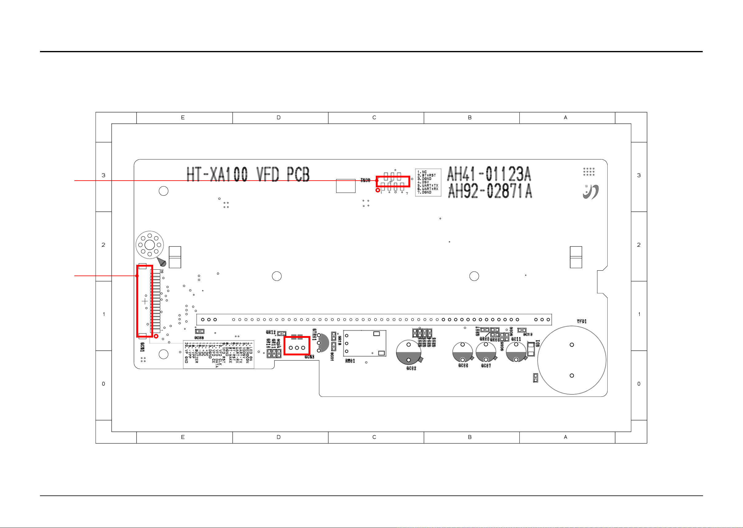
Samsung Electronics 6-3
PCB Diagram
6-2 VFD PCB Top
1
2
GCN1
GCN2
GCN3
Page 66
6-4 Samsung Electronics
PCB Diagram
6-2-1 Pin Connection
2 GCN1
VFD Control Signal
Pin No. Signal
1 GND
2 VH(42V)
3 VH(42V)
4 -VP
5 -VP
6 +VP
7 +VP
8 GND
9 CE
10 DATA
11 CLK
12 RESET
13 GND
14 BUZZER
15 BT_RESET
16 UART_RX
17 UART_TX
18 VDD_5V
19 REMOCON
20 LED_ON
1 GCN2
B/T Control Signal
Pin No. Signal
1 BT_WAKE
2 BT_RESET
3 GND
4 D5V
5 UART_TX
6 UART_RX
7 GND
Page 67
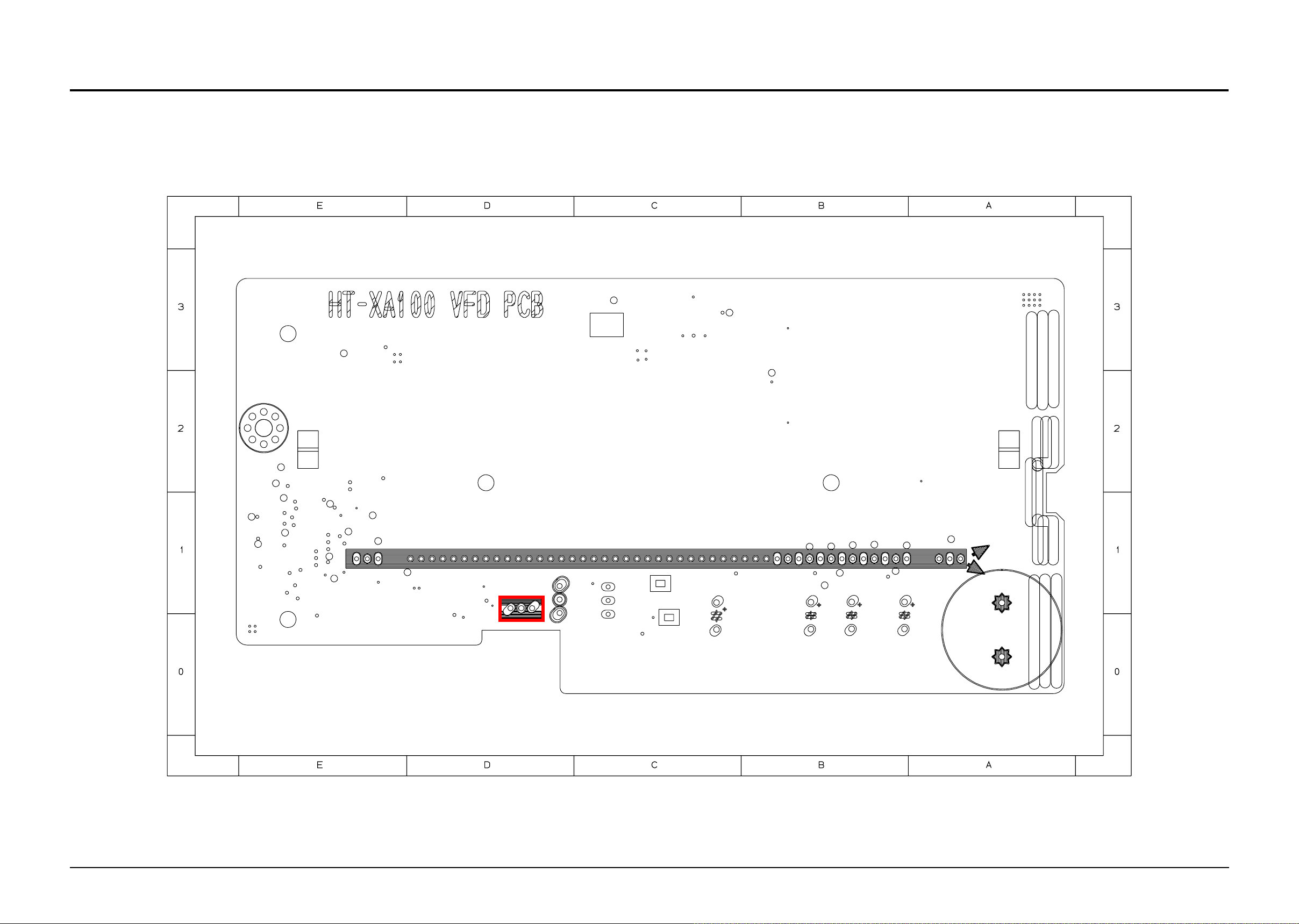
Samsung Electronics 6-5
PCB Diagram
6-3 VFD PCB Bottom
GCN3
Page 68

6-6 Samsung Electronics
PCB Diagram
6-4 AUX. SPK PCB Top
1
TP7
WCON2
JCN11
SPK01
Page 69

Samsung Electronics 6-7
PCB Diagram
6-4-1 Pin Connection
1 JCN11
Wireless signal Connector
Pin No. Signal
1 GND
2 CVBS
3 GND
4 V_T/G
5 GND
6 V_U/B
7 GND
8 V_V/R
9 GND
10 AUX_L
11 GND
12 AUX_R
13 GND
14 SCL
15 SDA
16 BCLK
17 LRCK
18 TSD1_WL
19 W_RST
20 W_ID
21 W_EINT
22 GND
23 VDD
24 GND
25 SPDIF_IN
26 GND
27 D5V
28 GND
6-4-2 Test Point Wave Form
TP7
Page 70
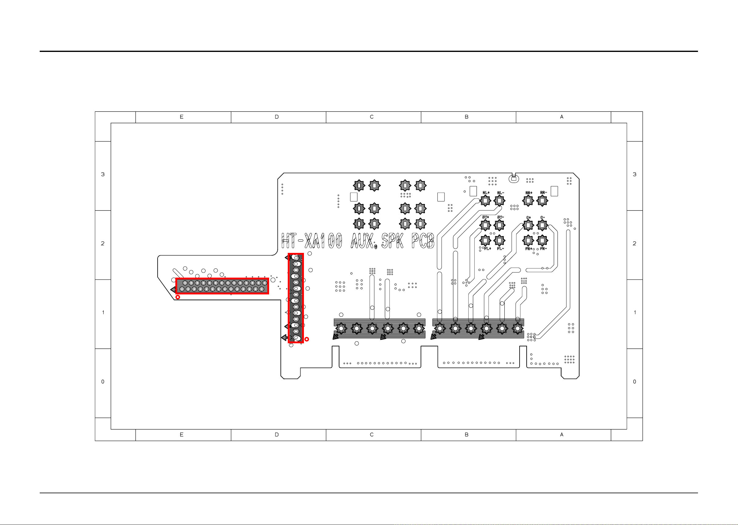
6-8 Samsung Electronics
PCB Diagram
6-5 AUX. SPK Bottom
WCON2
JCN11
Page 71

Samsung Electronics 6-9
PCB Diagram
6-6 AMP PCB Top
1
2
4
3
TP6
AIC8
AIC6
AIC7
CN01
AJ1
AV4
AV2
Page 72

6-10 Samsung Electronics
PCB Diagram
6-6-1 Pin Connection
1 AV2
Power Line Connector
Pin No. Signal
1 P_ON
2 P_SENSE
3 GND
4 U+5.6V
5 GND
6 +VFD
7 -VFD
8 -VFD
9 GND
10 GND
11 D5V
12 D5V
13 D3.3V
14 D3.3V
15 GND
2 AV4
Power Line Connector
Pin No. Signal
1 GND
2 U+5.6V
3 GND
4 +DC
5 -DC
6 VH(42V)
7 -12V
8 GND
9 GND
10 +12V
11 12V
12 D5V
13 D5V
14 D5V(8V)
15 GND
16 GND
17 GND
18 GND
19 D3.3V
20 D3.3V
21 D3.3V
22 P_ON
23 P_SENSE
3 CN01
AMP signal Connector
Pin No. Signal
1 P_FAN
2 FAN_SENSE
3 TI_RESET
4 TI_SD
5 GND
6 RR+
7 RR-
8 GND
9 RL+
10 RL-
11 GND
12 FR+
13 FR-
14 GND
15 FL+
16 FL-
17 GND
18 C+
19 C-
20 GND
21 SW+
22 SW-
23 GND
4 AJ1
AMP Power Connector
Pin No. Signal
1 GND
2 GND
3 GND
4 PVDD
5 PVDD
6 PVDD
7 +12V
8 GND
9 -12V
Page 73

Samsung Electronics 6-11
PCB Diagram
6-6-2 Test Point Wave Form
TP6
Page 74
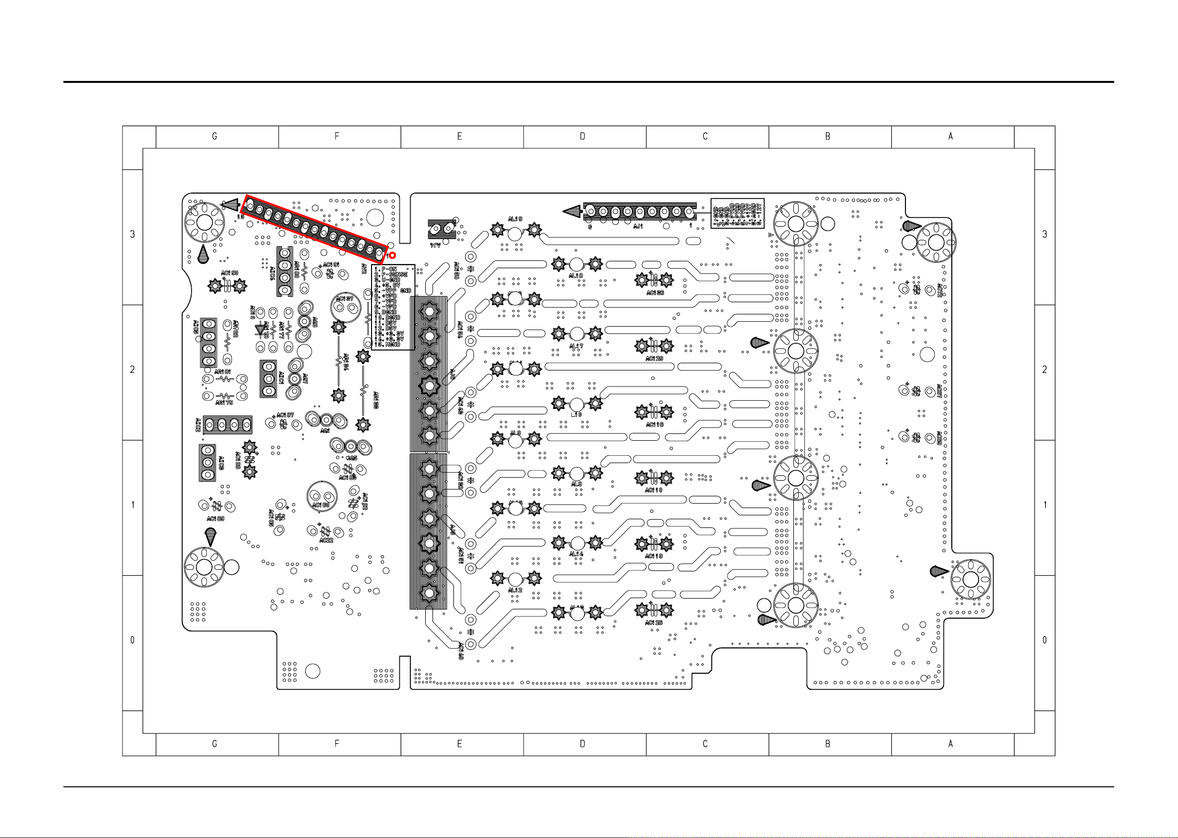
6-12 Samsung Electronics
PCB Diagram
6-7 AMP PCB Bottom
AV2
Page 75

Samsung Electronics 6-13
PCB Diagram
6-8 W/LESS. OPT PCB Top 6-9 W/LESS. OPT PCB Bottom
WCON3
WCON3
Page 76

6-14 Samsung Electronics
PCB Diagram
6-10 USB PCB Top
1 2
FCN11
UCN11
Page 77

Samsung Electronics 6-15
PCB Diagram
6-10-1 Pin Connection
1 FCN11
Aux1 Signal Connector
Pin No. Signal
1 GND
2 GND
3 LINE-R
4 GND
5 LINE-L
6 GND
7 HP-R
8 GND
9 HP-L
10 HP-SENSE
11 GND
12 L_IN_SEN
13 M_SEN_A
14 MIC-IN
15 +12V
2 UCN11
USB Signal Connector
Pin No. Signal
1 +5V
2 USB_D-
3 USB_D+
4 GND
Page 78

6-16 Samsung Electronics
PCB Diagram
6-11 USB PCB Bottom
UCN11
Page 79

Samsung Electronics 6-17
PCB Diagram
6-12 KEY PCB Top
FCN1
FWN1
Page 80
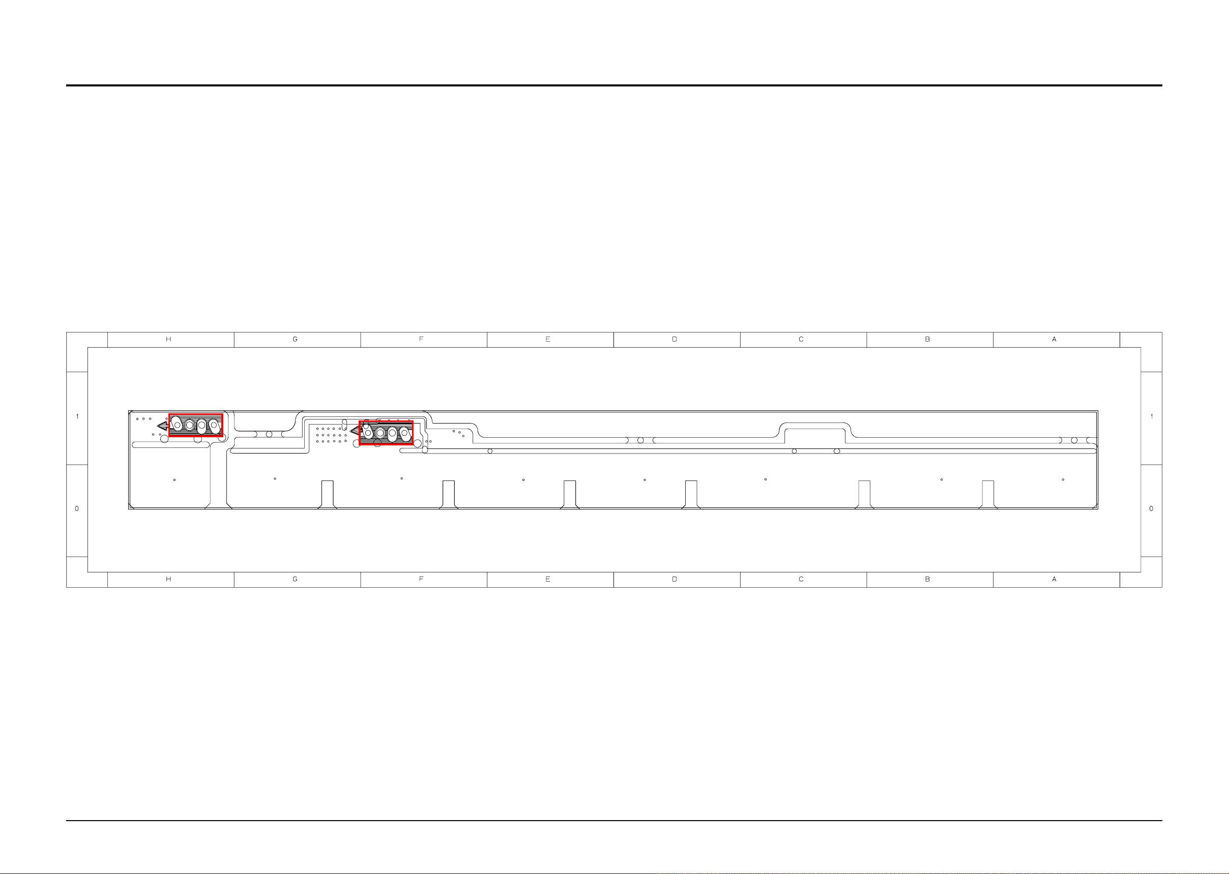
6-18 Samsung Electronics
PCB Diagram
6-13 KEY PCB Bottom
FCN1
FWN1
Page 81

Samsung Electronics 6-19
PCB Diagram
6-14 MAIN PCB Top
TP5
TP9
TP8
TP1
TP3
TP2
RIC4
RIC1
CIC1
UIC1
HIC1
MIC1
U1
XIC1
DIC1
DIC2
HCN1
CN09
CN6
Page 82

6-20 Samsung Electronics
PCB Diagram
6-14-1 Test Point Wave Form
TP1
TP9
TP2
TP3
TP5
TP8
Page 83

Samsung Electronics 6-21
PCB Diagram
6-15 MAIN PCB Bottom
TP4
1
2
3
4
5
6
TP10
TP11
MIC2
JIC01
ACN10
CN8
CN9
CN1
CN7
CN11
RCN3
RCN2
CN5
CN3
RCN1
CN2
JCN01
MIC3
MIC5
HPIC1
MIC6
MIC10
CIC2
AIC1
Page 84

6-22 Samsung Electronics
PCB Diagram
6-15-1 Pin Connection
1 ACN10
AMP Signal Connector
Pin No. Signal
1 P_FAN
2 FAN_SENSE
3 TI_RESET
4 TI_SD
5 GND
6 RR+
7 RR-
8 GND
9 RL+
10 RL-
11 GND
12 FR+
13 FR-
14 GND
15 FL+
16 FL-
17 GND
18 C+
19 C-
20 GND
21 SW+
22 SW-
23 GND
3 CN2
Power Line Connector
Pin No. Signal
1 GND
2 U+5.6V
3 GND
4 +DC
5 -DC
6 VH(42V)
7 -12V
8 GND
9 GND
10 +12V
11 12V
12 D5V
13 D5V
14 D5V(8V)
15 GND
16 GND
17 GND
18 GND
19 D3.3V
20 D3.3V
21 D3.3V
22 P_ON
23 P_SENSE
4 CN3
VFD Control Signal
Pin No. Signal
1 GND
2 VH(42V)
3 VH(42V)
4 -VP
5 -VP
6 +VP
7 +VP
8 GND
9 CE
10 DATA
11 CLK
12 RESET
13 GND
14 BUZZER
15 BT_RESET
16 UART_RX
17 UART_TX
18 VDD_5V
19 REMOCON
20 LED_ON
2 JCN01
Wireless signal Connector
Pin No. Signal
1 GND
2 CVBS
3 GND
4 V_T/G
5 GND
6 V_U/B
7 GND
8 V_V/R
9 GND
10 AUX_L
11 GND
12 AUX_R
13 GND
14 SCL
15 SDA
16 BCLK
17 LRCK
18 TSD1_WL
19 W_RST
20 W_ID
21 W_EINT
22 GND
23 VDD
24 GND
25 SPDIF_IN
26 GND
27 D5V
28 GND
5 CN5
USB Signal Connector
Pin No. Signal
1 +5V
2 USB_D-
3 USB_D+
4 GND
6 CN11
Aux1 Signal Connector
Pin No. Signal
1 GND
2 GND
3 LINE-R
4 GND
5 LINE-L
6 GND
7 HP-R
8 GND
9 HP-L
10 HP-SENSE
11 GND
12 L_IN_SEN
13 M_SEN_A
14 MIC-IN
15 +12V
Page 85

Samsung Electronics 6-23
PCB Diagram
6-15-2 Test Point Wave Form
TP4
TP10
TP11
Page 86

6-24 Samsung Electronics
PCB Diagram
6-16 BLUETOOTH PCB Top 6-17 BLUETOOTH PCB Bottom
CON1
IC1
Page 87

Samsung Electronics 6-25
PCB Diagram
6-18 POWER PCB Top 6-19 POWER PCB Bottom
FCN3
Page 88

6-26 Samsung Electronics
PCB Diagram
6-20 SMPS PCB Top
CN2
CN3
ICMI
Page 89

Samsung Electronics 7-1
Schematic Diagram
This Document can not be used without Samsung’s authorization.
7. Schematic Diagram
7-1 Overall Block Diagram ..................................................................................... 7-2
7-2 AMP_USB ......................................................................................................... 7-3
7-3 AMP_VIDEO JACK ...........................................................................................
7-4
7-4 AMP_SPK .......................................................................................................... 7-5
7-5 AMP_VFD .......................................................................................................... 7-6
7-6 AMP_POWER ................................................................................................... 7-7
7-7 KEY_FUNC ........................................................................................................ 7-8
7-8 KEY_POWER .................................................................................................... 7-9
7-9 MAIN_MICOM ................................................................................................... 7-10
7-10 MAIN_HDMI ....................................................................................................... 7-11
7-11 MAIN_DSP ......................................................................................................... 7-12
7-12 MAIN_PWM ....................................................................................................... 7-13
7-13 MAIN_VIDEO ..................................................................................................... 7-14
7-14 MAIN_MPEG ..................................................................................................... 7-15
7-15 SMPS ................................................................................................................. 7-16
Page 90
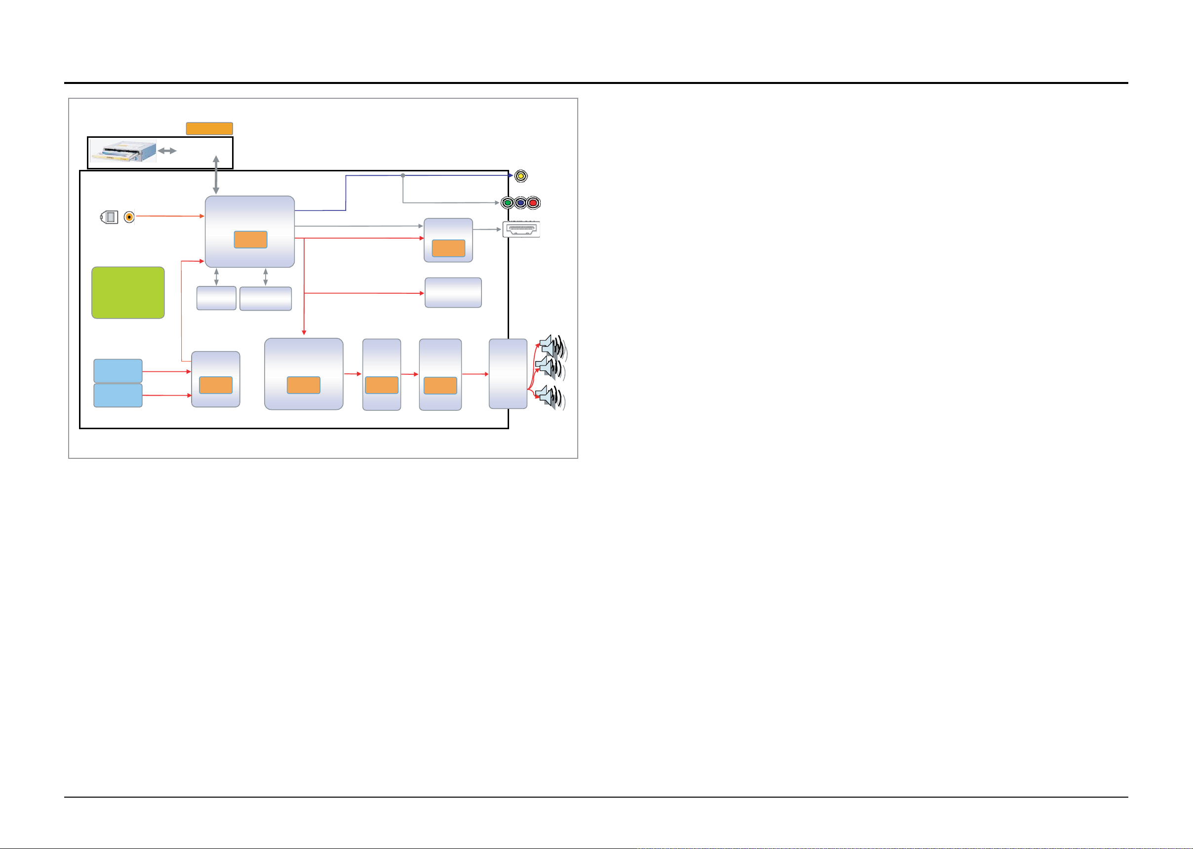
7-2 Samsung Electronics
Schematic Diagram
This Document can not be used without Samsung’s authorization.
7-1 Overall Block Diagram
LOADER
DVD Engine
128MB
DDR2
SATAI I/F
Digital Audio (I2S)
CVBS
Y Pb Pr
Digital Video
HDMI TX
SPDIF
I2S/SPDIF
Analog Video
Program
PWM
PS9829B
Digital
Amp
SYSTEM
MICOM
SPK
Optic IN
A/DC
Wireless
-Ready
MPEG
AUDIO DSP
TAS5142
ES7108
Tuner
AUX1/2
64MB
NOR Flash
CS5345 CS48540
ES8391
In terms of AUDIO.
In Digital In mode, SPDIF signal goes into MPEG (ES8391).
In AUX ½, TUNER mode, Analog Audio signal goes into A/DC (CS5345) and converted I2S signal and goes to
MPEG (ES8391).
MPEG (ES8391) outputs I2S and it goes into DSP (CS48540) and Equalized and it goes into PWM (PS9829B).
The output signal of PWM (PS9829B) goes into AMP (TAS5142) and it is SPEAKER Output.
In terms of VIDEO.
DVD Loader outputs RF signal and MPEG (ES8391) get RF signal and Decoded.
MPEG (ES8391) outputs Analog Video signal (Composite, Component Video) and outputs 32bits Digital Video signal to
HDMI TX (ES7108) and it converted TMDS signal and it is HDMI video Output.
Page 91

Samsung Electronics 7-3
Schematic Diagram
This Document can not be used without Samsung’s authorization.
7-2 AMP_USB
AUDIO SIGNAL
Page 92

7-4 Samsung Electronics
Schematic Diagram
This Document can not be used without Samsung’s authorization.
7-3 AMP_VIDEO JACK
AUDIO SIGNAL
AUDIO CLOCK
VIDEO SIGNAL
Page 93
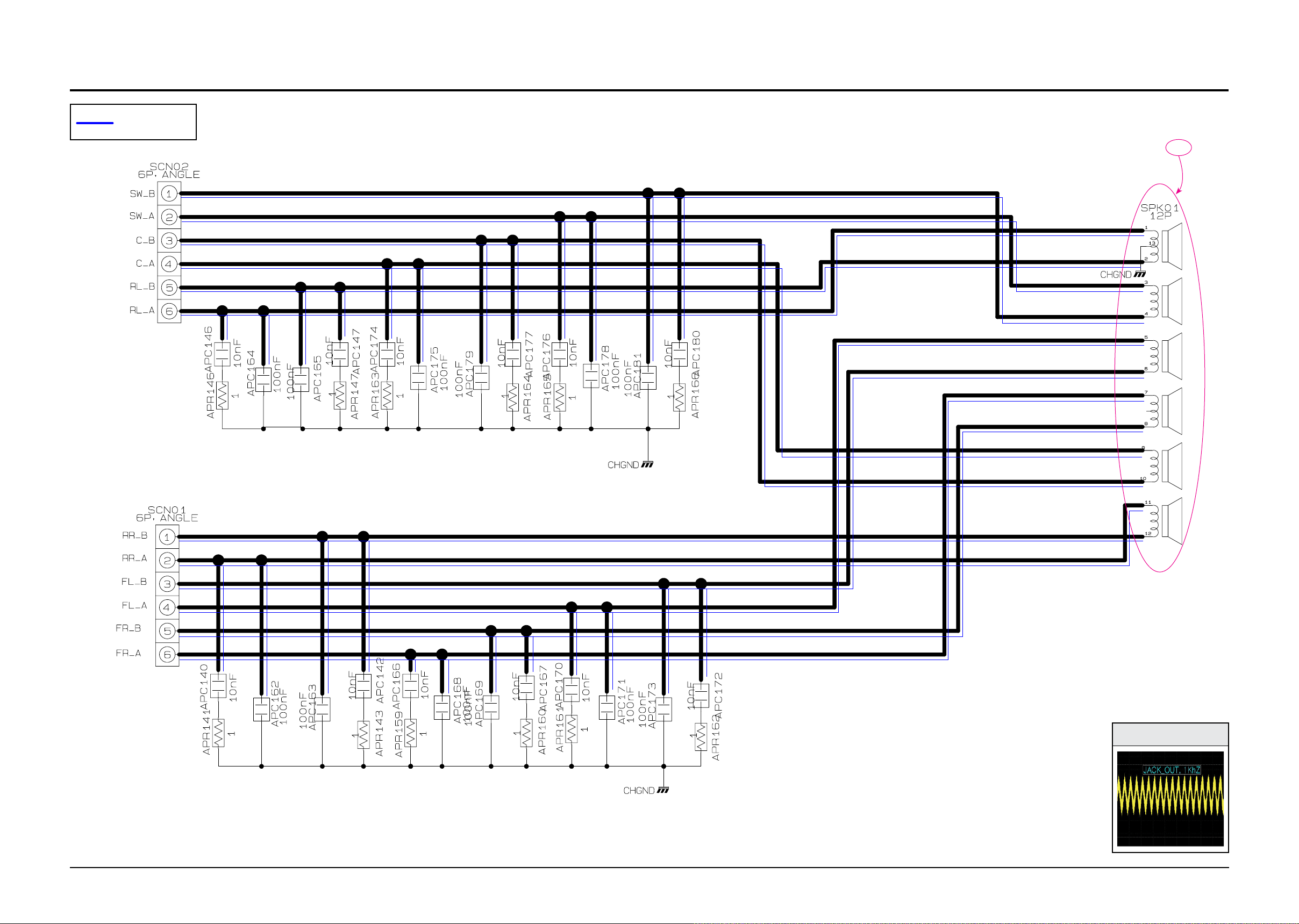
Samsung Electronics 7-5
Schematic Diagram
This Document can not be used without Samsung’s authorization.
7-4 AMP_SPK
TP7
AUDIO SIGNAL
TP7
Page 94

7-6 Samsung Electronics
Schematic Diagram
This Document can not be used without Samsung’s authorization.
7-5 AMP_VFD
BUZZER SIGNAL
VFD CONTROL SIGNAL
Page 95
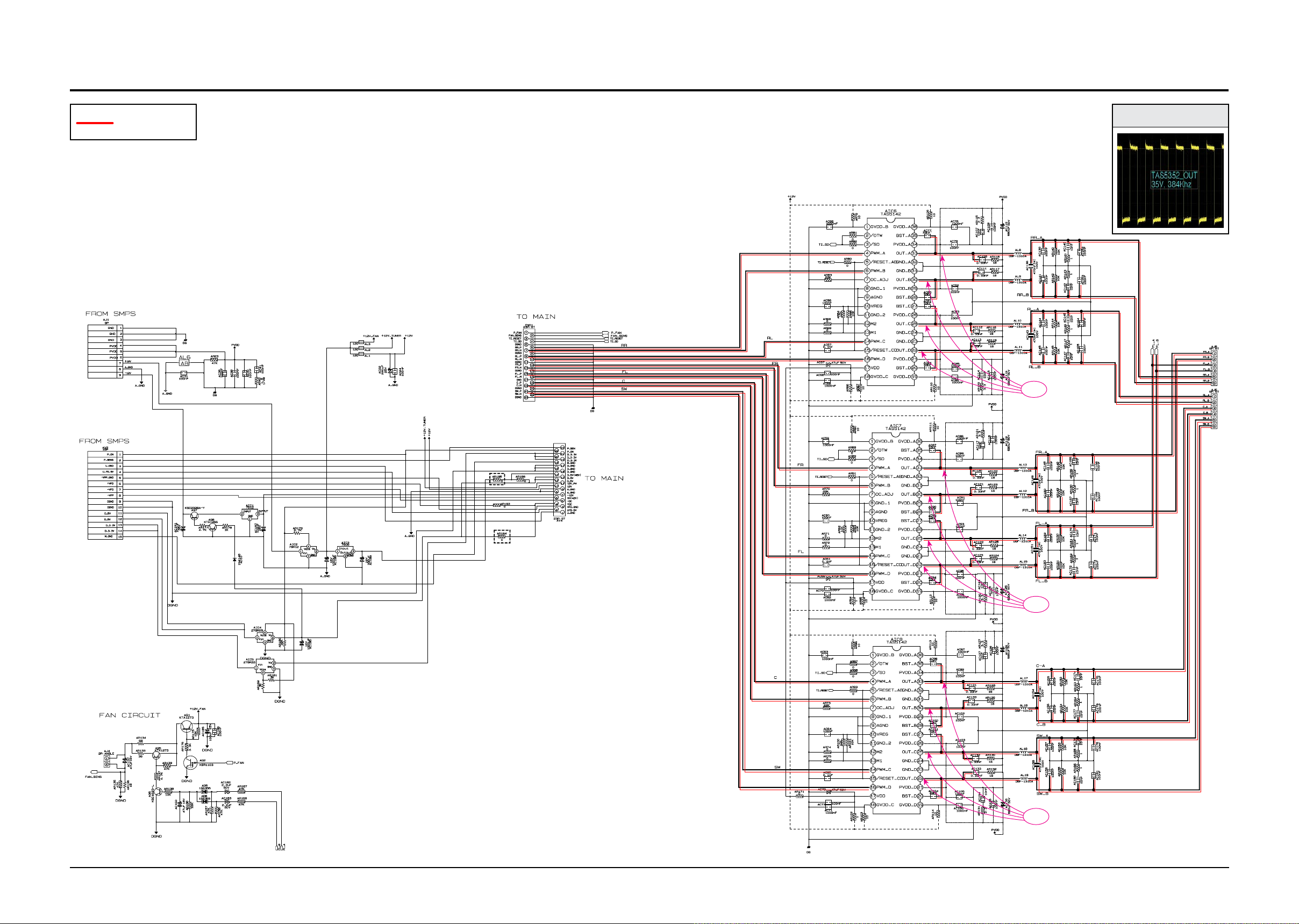
Samsung Electronics 7-7
Schematic Diagram
This Document can not be used without Samsung’s authorization.
7-6 AMP_POWER
AUDIO SIGNAL
TP6
TP6
TP6
TP6
Page 96

7-8 Samsung Electronics
Schematic Diagram
This Document can not be used without Samsung’s authorization.
7-7 KEY_FUNC
KEY SIGNAL
Page 97

Samsung Electronics 7-9
Schematic Diagram
This Document can not be used without Samsung’s authorization.
7-8 KEY_POWER
POWER KEY SIGNAL
Page 98

7-10 Samsung Electronics
Schematic Diagram
This Document can not be used without Samsung’s authorization.
7-9 MAIN_MICOM
AUDIO SIGNAL
MICOM +5V
Page 99

Samsung Electronics 7-11
Schematic Diagram
This Document can not be used without Samsung’s authorization.
7-10 MAIN_HDMI
AUDIO SIGNAL
TMDS DATA (HDMI)
AUDIO CLOCK
VIDEO SIGNAL
TP9
TP9
Page 100

7-12 Samsung Electronics
Schematic Diagram
This Document can not be used without Samsung’s authorization.
7-11 MAIN_DSP
AUDIO SIGNAL
AUDIO CLOCK
 Loading...