

Page 1
GSM TELEPHONE
GT-S5200
GSM TELEPHONE
CONTENTS
Safety Precautions
1.
Specification
2.
Product Function
3.
Array course control
4.
Exploded View and Parts list
5.
MAIN Electrical Parts List
6.
Disassembly and Assembly
7.
Instructions
Block Diagrams
8.
PCB Diagrams
9.
Chart of Troubleshooting
10.
Reference data
11.
Page 2

Safety Precautions
1.
Repair Precaution
1-1.
Repair in Shield Box, during detailed tuning.
●
Take specially care of tuning or test,
because specipicty of cellular phone is sensitive for surrounding interference(RF noise).
Be careful to useakind of magnetic object or tool,
●
because performance of parts is damaged by the influence of manetic force.
Surely useastandard screwdriver when you disassemble this product,
●
otherwise screw will be worn away.
Useathicken twisted wire when you measure level.
●
thicken twisted wire has low resistance, therefore error of measurement is few.
A
Repair after separate Test Pack and Set because for short danger(for example an
●
overcurrent and furious flames of parts etc) when you repair board in condition of
connecting Test Pack and tuning on.
Take specially care of soldering, because Land of PCB is small and weak in heat.
●
Surely tune on/off while using AC power plug, becausearepair of battery charger is
●
dangerous when tuning ON/OFF PBA and Connector after disassembing charger.
Don't use as you pleases after change other material than replacement registered on SEC
●
System.
Otherwise engineer in charge isn't charged with problem that you don't keep this rules.
1-1
SAMSUNG Proprietary-Contents may change without notice
This Document can not be used without Samsung's authorization
Page 3

Safety Precautions
ESD(Electrostatically Sensitive Devices) Precaution
1-2.
Several semiconductor may be damaged easilly by static electricity. Such parts are called by
ESD(Electrostatically Sensitive Devices), for example IC,BGA chip etc. Read Precaution below.
You can prevent from ESD damage by static electricity.
Remove static electricity remained your body before you touch semiconductor or parts with
●
semiconductor. There are ways that you touch an earthed place or wear static electricity
prevention string on wrist.
Use earthed soldering steel when you connect or disconnect ESD.
●
Use soldering removing tool to break static electricity.,otherwise ESD will be damaged by
●
static electricity.
Don't unpack until you set up ESD on product. Because most of ESD are packed by box
●
and aluminum plate to have conductive power,they are prevented from static electricity.
You must maintain electric contact between ESD and place due to be set up until ESD is
●
connected completely to the proper place oracircuit board.
1-2
SAMSUNG Proprietary-Contents may change without notice
This Document can not be used without Samsung's authorization
Page 4
Specification
2.
GSM General Specification
2-1.
GSM850 EGSM900 DCS1800 PCS1900
Freq. Band[MHz]
Uplink/Downlink
ARFCN range 128-251
Tx/Rx spacing 45MHz 45MHz 95MHz 80 MHz
Mod. Bit rate
/BitPeriod
Time Slot Period
/ Frame Period
Modulation 0.3GMSK 0.3GMSK 0.3GMSK 0.3GMSK
824-849
869-894
270.833kbps
3.692us
576.9us
4.615ms
880~915
925~960
0~124 &
975~1023
270.833kbps
3.692us
576.9us
4.615ms
1710~1785
1805~1880
512~885 512~810
270.833kbps
3.692us
576.9us
4.615ms
1850~1910
1930~1990
270.833kbps
3.692 us
576.9 us
4.615 ms
MS Power 33dBm~5dBm 33dBm~5dBm 30dBm~0dBm 30dBm~0dBm
Power Class 5~19(
Sensitivity -102dBm -102dBm -100dBm -100dBm
TDMAMux8888
Cell Radius 35Km 35Km 2Km 2 Km
SAMSUNG Proprietary-Contents may change without notice
class
4) 5~19(
This Document can not be used without Samsung's authorization
2-1
class
4) 0~15(
class1)
0~15(
class1)
Page 5
Specification
GSM TX power class
2-2.
TX Power
control level
533±2
631±2
729±2
827±2
925±2
10 23±2
11 21±2
GSM850 GSM900
dBm
dBm
dBm
dBm
dBm
dBm
dBm
33±2
31±2
29±2
27±2
25±2
23±2
21±2
dBm
dBm
dBm
dBm
dBm
dBm
dBm
TX Power
control level
030±3
128±3
226±3
324±3
422±3
520±3
618±3
DCS1800 PCS1900
dBm
dBm
dBm
dBm
dBm
dBm
dBm
30±3
28±3
26±3
24±3
22±3
20±3
18±3
dBm
dBm
dBm
dBm
dBm
dBm
dBm
12 19±2
13 17±2
14 15±2
15 13±2
16 11±3
17 9±3
18 7±3
19 5±3
dBm
dBm
dBm
dBm
dBm
dBm
dBm
dBm
19±2
17±2
15±2
13±2
11±3
9±3
7±3
5±3
dBm
dBm
dBm
dBm
dBm
dBm
dBm
dBm
716±3
814±3
912±4
10 10±4
11 8±4
12 6±4
13 4±4
14 2±5
dBm
dBm
dBm
dBm
dBm
dBm
dBm
dBm
16±3
14±3
12±4
10±4
8±4
6±4
4±4
2±5
dBm
dBm
dBm
dBm
dBm
dBm
dBm
dBm
15 0±5
2-2
SAMSUNG Proprietary-Contents may change without notice
This Document can not be used without Samsung's authorization
dBm
0±5
dBm
Page 6

Operation Instruction and Installation
3.
Main Function
Quad Band(GSM850+EGSM900+DCS1800+PCS1900)
GPRS Rx/Tx, EDGE Rx/Tx
FM Radio
Bluetooth v2.1
TFT LCD
-
AF Camera
-3M
Music Player(MP3, AAC, AAC+, eAAC+)
MicroSD
-
2.2"
QVGA
262K
Color
3-1
SAMSUNG Proprietary-Contents may change without notice
This Document can not be used without Samsung's authorization
Page 7
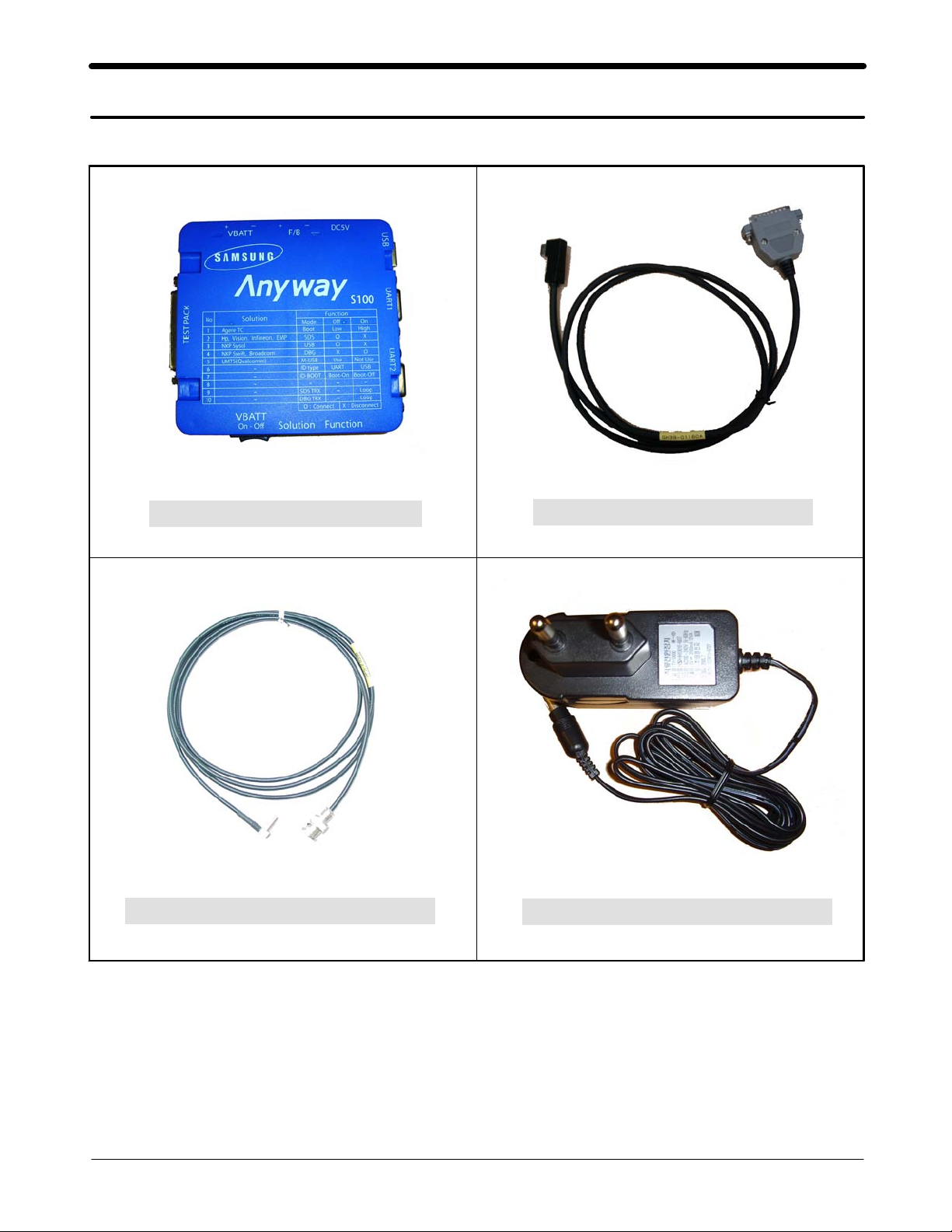
Array course control
4.
Software Adjustments
4-1.
Test Jig(GH99
RF Test Cable(GH
-36900
39-00985
A)
A)
Test Cable(GH
Adapter(GH
39-01160
99-38251
A)
A)
4-1
SAMSUNG Proprietary-Contents may change without notice
This Document can not be used without Samsung's authorization
Page 8

Array course control
Software Downloading
4-2.
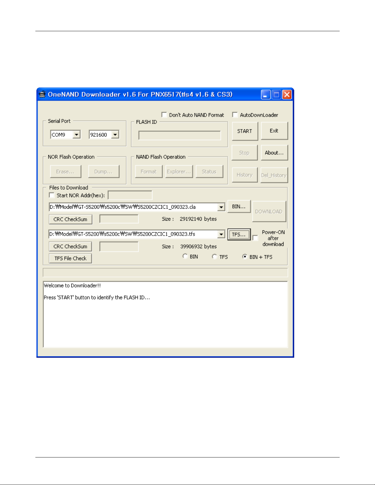
4-2-1
4-2-2.
Downloading Binary Files
binary files for downloading GT-S5200C
•2
S5200XIID3_CLA
S5200XIID3_TFS
-
Pre-request for Downloading
Downloader Program(OneNAND Downloader V1.2 Lite for PNX6517)
•
GT-S5200C Mobile Phone
•
JIG Box
•
Test Cable
•
Serial Cable
•
Binary file, TFS file
•
4-2
SAMSUNG Proprietary-Contents may change without notice
This Document can not be used without Samsung's authorization
Page 9
Array course control
4-2-3.
1
S/W Downloader Program
Load the binary download program by executing the OneNAND Downloader V1.
.
Lite for PNX6517
6
4-3
SAMSUNG Proprietary-Contents may change without notice
This Document can not be used without Samsung's authorization
Page 10
Array course control
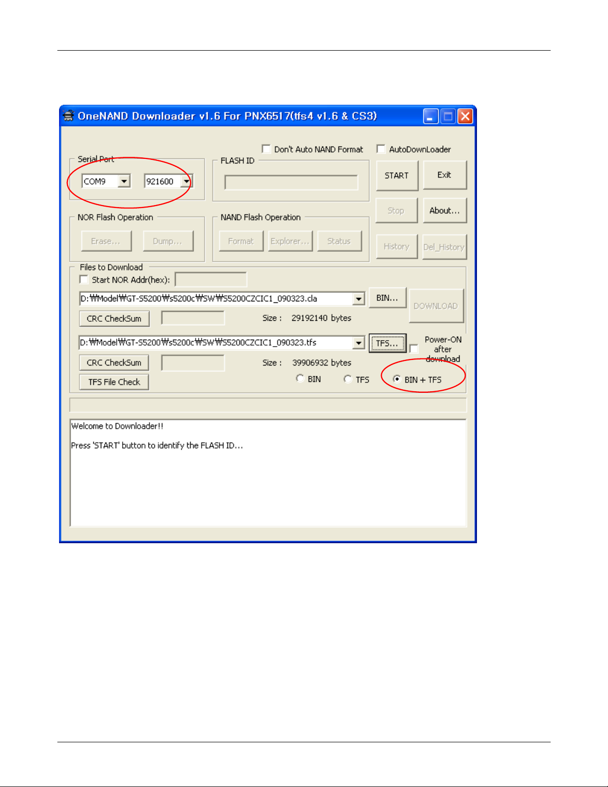
Select the Port, Baud Rate and Mode
.
2
4-4
SAMSUNG Proprietary-Contents may change without notice
This Document can not be used without Samsung's authorization
Page 11
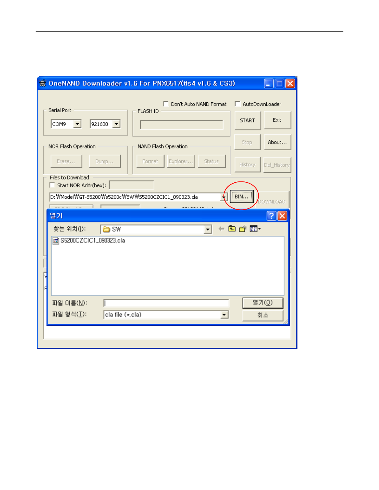
Select the file(s) what you want to download
.
3
Array course control
4-5
SAMSUNG Proprietary-Contents may change without notice
This Document can not be used without Samsung's authorization
Page 12
Array course control
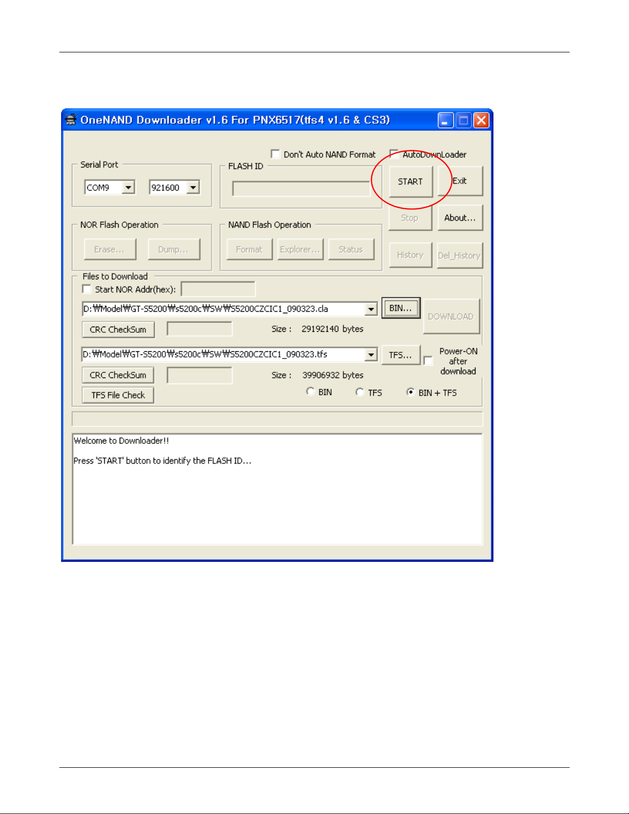
Press the"Start" button and connect the Handset
.
4
4-6
SAMSUNG Proprietary-Contents may change without notice
This Document can not be used without Samsung's authorization
Page 13
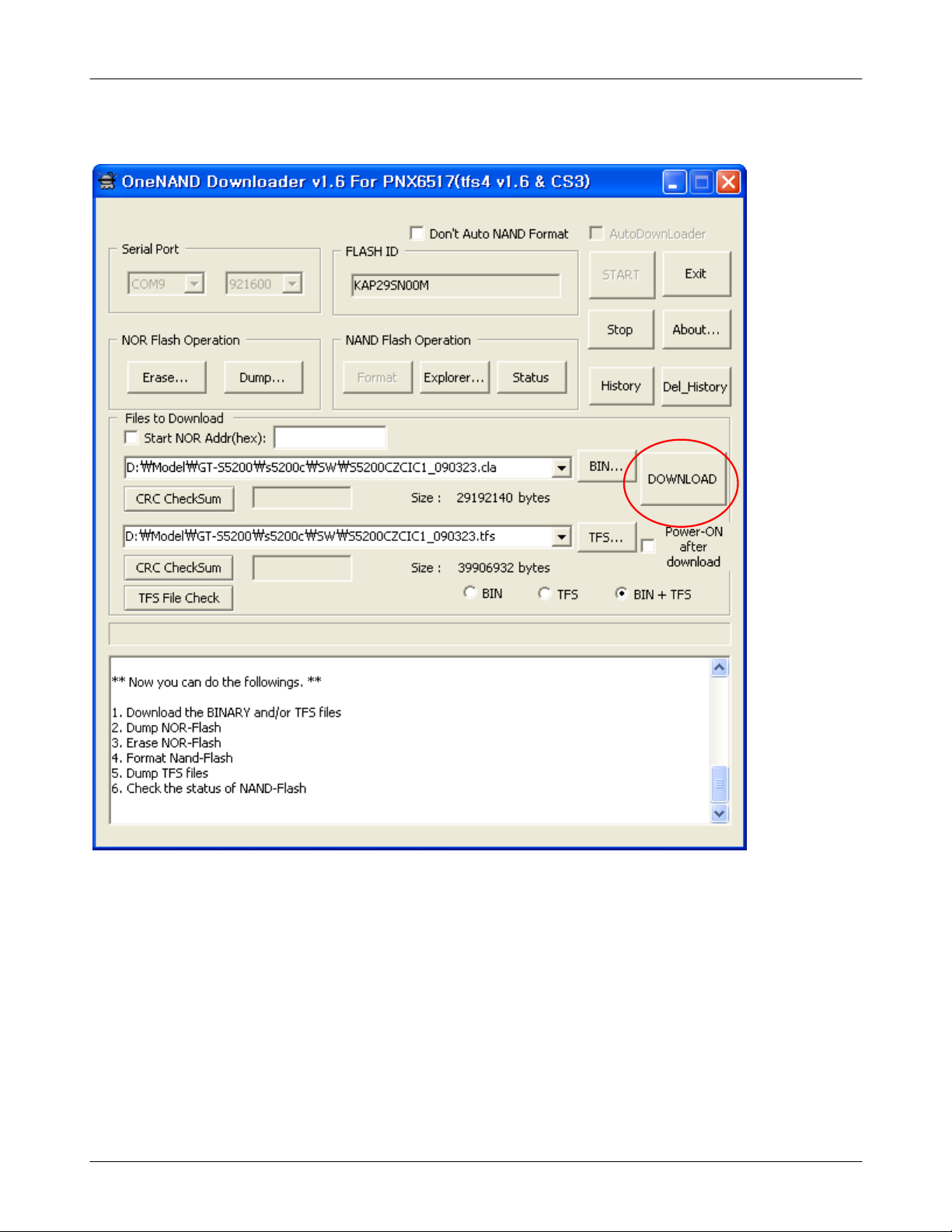
Press the"Download" button.
.
5
Array course control
4-7
SAMSUNG Proprietary-Contents may change without notice
This Document can not be used without Samsung's authorization
Page 14
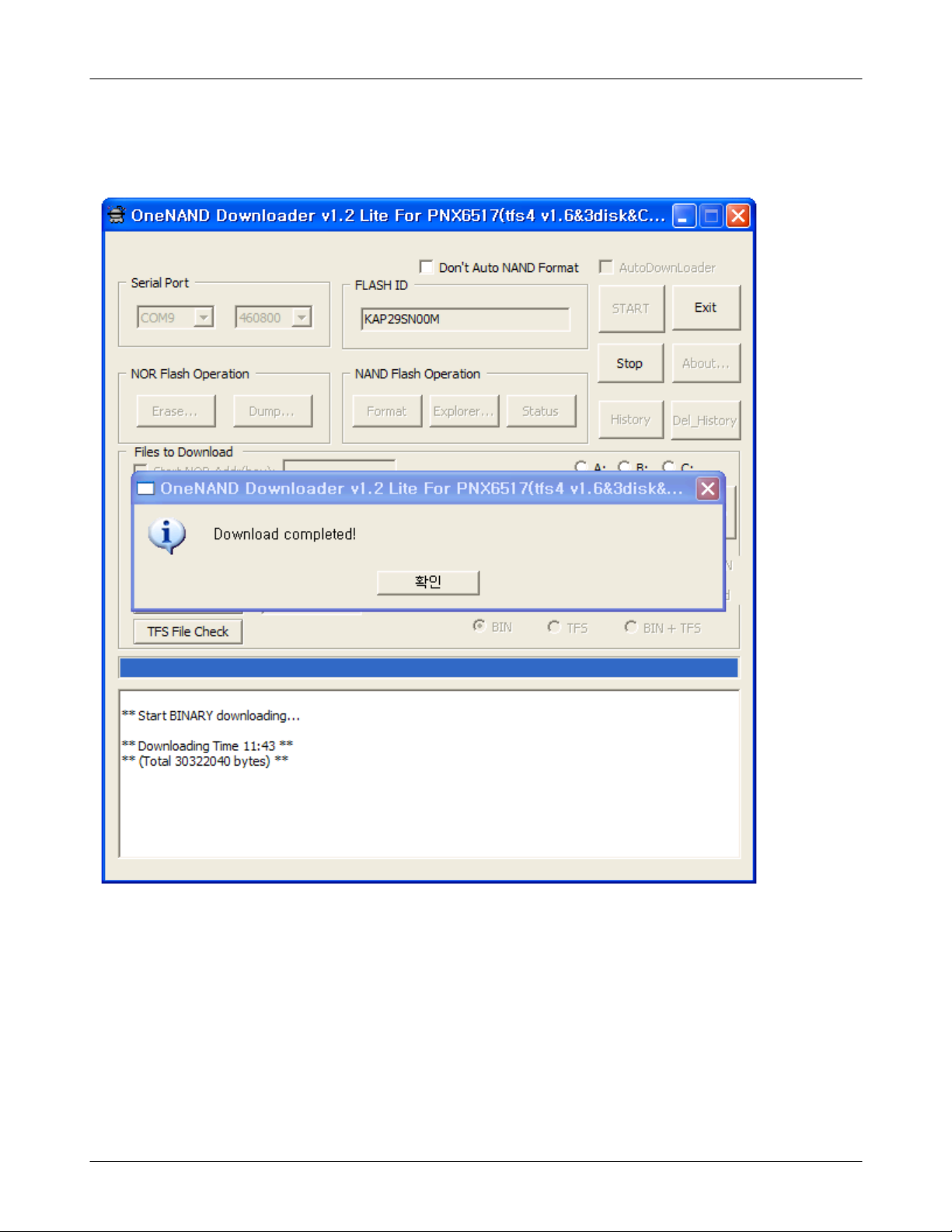
Array course control
When downloading is complete, automatically the small window was showed up.
.
6
4-8
SAMSUNG Proprietary-Contents may change without notice
This Document can not be used without Samsung's authorization
Page 15
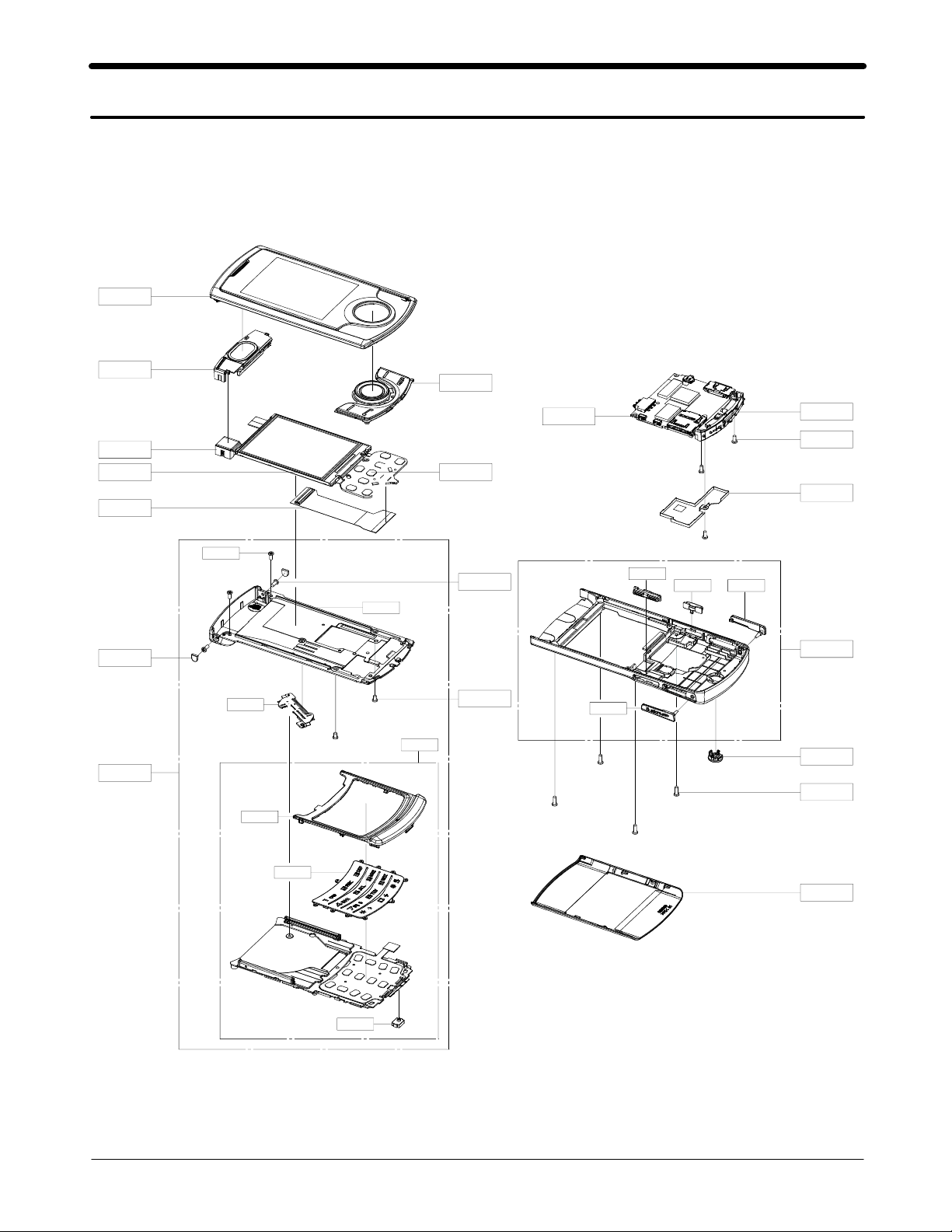
Exploded View and Parts List
5.
5-1.
QFU01
QSP01
QCA01
QLC01
QPC01
Cellular phone Exploded View
QKP02
QME02
QCR03
QCR03
QFL01
QMP01
QVO01
QAN02
QCR05
QSH01
QCK01 QIF01
QSC01
QFL00
QHI01
QFR04
QKP01
QMI03
QFR01
QCR47
QRE01
QSD01
QRF01
QCR60
QBA00
5-1
SAMSUNG Proprietary-Contents may change without notice
This Document can not be used without Samsung's authorization
Page 16
Exploded View and Parts List
5-2.
Cellular phone Parts list
Design LOC Discription SEC CODE
QCR03
QCR05
QCR47
QCR60
QFU01
QKP02
QLC01
QME02
QMP01
QPC01
QRF01
QSC01
QSH01
QSP01
SCREW-MACHINE
SCREW-MACHINE
SCREW-MACHINE
SCREW-MACHINE
ASSY CASE-UPPER GH98-12457A
ASSY KEYPAD-SUB(OPEN/BLU) GH98-12464A
LCD-2.2'' QVGA GH07-01436A
DOME SHEET-GT-S5200 SUB9KEY GH59-07099A
A/S ASSY-PBA MAIN,GT_S5200,CIT,EU(SVC) GH82-03780A
ASSY ETC-SLIDE FPCB(GT-S5200) GH59-07060A
PMO COVER-RF GH72-53104A
TAPE-SCREW CAP GH74-44383A
ICT SHIELD-CAN GH70-04940A
MODULE-SPK/MOT MODULE(GT-S5200) GH59-07093A
6001-001811
6001-001478
6001-001695
6001-002005
QRE01
QFL00
QIF01
QSD01
QCK01
QVO01
QHI01
QFL01
QFR01
ASSY CASE-REAR GH98-12456A
QMI03 ASSY RUBBER-MIC HOLDER GH98-13556A
QFR04 ASSY CASE-FRONT BUSH GH98-13691A
QKP01 ASSY KEYPAD-MAIN(OPEN/BLU) GH98-12463A
QCR03 SCREW-MACHINE
PMO COVER-IF GH72-53106A
PMO COVER-SD GH72-53107A
PMO KEY-CAMERA GH72-53112A
PMO KEY-VOLUME GH72-53113A
ASSY CASE-SLIDE GH98-12460A
ASSY HINGE-ACTUATOR GH98-12122A
ASSY CASE-LOWER GH98-12461A
ASSY CASE-FRONT GH98-12459A
6001-001811
5-1
This Document can not be used without Samsung's authorization
Page 17
MAIN Electrical Parts List
6.
SEC CODE Design LOD Discription
0202-001602
0202-001602
0202-001602
0202-001602
0202-001602
0403-001749
0403-001749
0406-001286
0406-001286
0406-001288
0406-001288
0406-001288
0406-001288
0406-001288
0406-001288
0406-001288
0406-001305
0406-001361
1009-001035
1108-000268
1201-002773
1203-004857
1203-005512
1203-005728
1204-003020
1205-003517
1205-003653
1205-003696
1404-001221
2007-000140
2007-000141
2007-000143
2007-000143
2007-000148
2007-000148
2007-000149
R100 SOLDER-CREAM
R300 SOLDER-CREAM
R313 SOLDER-CREAM
R400 SOLDER-CREAM
R408 SOLDER-CREAM
ZD500 DIODE-ZENER
ZD502 DIODE-ZENER
ZD400 DIODE-TVS
ZD501 DIODE-TVS
ZD200 DIODE-TVS
ZD201 DIODE-TVS
ZD404 DIODE-TVS
ZD405 DIODE-TVS
ZD503 DIODE-TVS
ZD504 DIODE-TVS
ZD505 DIODE-TVS
F401 DIODE-TVS
ZD402 DIODE-TVS
U302 IC-HALL EFFECT S/W
UME200 IC-MCP
PAM100 IC-POWER AMP
U500 IC-DC/DC CONVERTER
U301 IC-POSI.FIXED REG
U300 IC-POWER SUPERVISOR
U400 IC-DEMODULATOR
U101 IC-BLUETOOTH
UCP200 IC-MODEM
U100 IC-TRANSCEIVER
VR500 THERMISTOR-NTC
R207 R-CHIP
R309 R-CHIP
R401 R-CHIP
R409 R-CHIP
R310 R-CHIP
R500 R-CHIP
R206 R-CHIP
6-1
SAMSUNG Proprietary-Contents may change without notice
This Document can not be used without Samsung's authorization
Page 18

Main Electrical Parts List
SEC CODE Design LOD Discription
2007-000152
2007-000157
2007-000157
2007-000157
2007-000157
2007-000157
2007-000160
2007-000162
2007-000162
2007-000166
2007-000170
2007-000170
2007-000172
2007-000172
2007-000172
2007-000242
2007-000242
2007-000758
2007-001292
2007-001292
2007-001319
2007-001319
2007-001333
2007-001333
2007-001333
2007-002796
2007-003015
2007-007573
2007-007589
2007-007875
2007-007981
2007-008354
2007-008354
2203-000233
2203-000233
2203-000254
R501 R-CHIP
R402 R-CHIP
R403 R-CHIP
R404 R-CHIP
R405 R-CHIP
R406 R-CHIP
R107 R-CHIP
R502 R-CHIP
R503 R-CHIP
R413 R-CHIP
R414 R-CHIP
R415 R-CHIP
R103 R-CHIP
R311 R-CHIP
R312 R-CHIP
R416 R-CHIP
R420 R-CHIP
R504 R-CHIP
R307 R-CHIP
R308 R-CHIP
R201 R-CHIP
R202 R-CHIP
R317 R-CHIP
R318 R-CHIP
R411 R-CHIP
R417 R-CHIP
R105 R-CHIP
R303 R-CHIP
R505 R-CHIP
R316 R-CHIP
R315 R-CHIP
C504 R-CHIP
R304 R-CHIP
C106 C-CER,CHIP
C418 C-CER,CHIP
C135 C-CER,CHIP
6-2
SAMSUNG Proprietary-Contents may change without notice
This Document can not be used without Samsung's authorization
Page 19

Main Electrical Parts List
SEC CODE Design LOD Discription
2203-000278
2203-000311
2203-000311
2203-000386
2203-000438
2203-000438
2203-000438
2203-000466
2203-000627
2203-000627
2203-000627
2203-000812
2203-000995
2203-000995
2203-000995
2203-000995
2203-000995
2203-001221
2203-005050
2203-005050
2203-005050
2203-005050
2203-005052
2203-005053
2203-005057
2203-005281
2203-005281
2203-005395
2203-005444
2203-005481
2203-005481
2203-005482
2203-005482
2203-005482
2203-005483
2203-005552
C411 C-CER,CHIP
C336 C-CER,CHIP
C413 C-CER,CHIP
C127 C-CER,CHIP
C130 C-CER,CHIP
C401 C-CER,CHIP
C402 C-CER,CHIP
C101 C-CER,CHIP
C134 C-CER,CHIP
C328 C-CER,CHIP
C331 C-CER,CHIP
C114 C-CER,CHIP
C137 C-CER,CHIP
C316 C-CER,CHIP
C342 C-CER,CHIP
C407 C-CER,CHIP
C414 C-CER,CHIP
C124 C-CER,CHIP
C107 C-CER,CHIP
C108 C-CER,CHIP
C117 C-CER,CHIP
C118 C-CER,CHIP
C112 C-CER,CHIP
C146 C-CER,CHIP
C416 C-CER,CHIP
C139 C-CER,CHIP
C140 C-CER,CHIP
C122 C-CER,CHIP
C136 C-CER,CHIP
C409 C-CER,CHIP
C412 C-CER,CHIP
C207 C-CER,CHIP
C211 C-CER,CHIP
C312 C-CER,CHIP
C217 C-CER,CHIP
C110 C-CER,CHIP
6-3
SAMSUNG Proprietary-Contents may change without notice
This Document can not be used without Samsung's authorization
Page 20

Main Electrical Parts List
SEC CODE Design LOD Discription
2203-005552
2203-005552
2203-005552
2203-006048
2203-006048
2203-006048
2203-006048
2203-006048
2203-006048
2203-006048
2203-006048
2203-006048
2203-006048
2203-006048
2203-006048
2203-006048
2203-006048
2203-006048
2203-006048
2203-006137
2203-006137
2203-006201
2203-006208
2203-006208
2203-006208
2203-006208
2203-006257
2203-006257
2203-006260
2203-006260
2203-006260
2203-006260
2203-006324
2203-006348
2203-006399
2203-006399
C113 C-CER,CHIP
C119 C-CER,CHIP
C120 C-CER,CHIP
C138 C-CER,CHIP
C203 C-CER,CHIP
C205 C-CER,CHIP
C210 C-CER,CHIP
C213 C-CER,CHIP
C220 C-CER,CHIP
C315 C-CER,CHIP
C324 C-CER,CHIP
C329 C-CER,CHIP
C341 C-CER,CHIP
C343 C-CER,CHIP
C404 C-CER,CHIP
C408 C-CER,CHIP
C410 C-CER,CHIP
C415 C-CER,CHIP
C501 C-CER,CHIP
C123 C-CER,CHIP
C144 C-CER,CHIP
C301 C-CER,CHIP
C332 C-CER,CHIP
C333 C-CER,CHIP
C334 C-CER,CHIP
C335 C-CER,CHIP
C405 C-CER,CHIP
C406 C-CER,CHIP
C317 C-CER,CHIP
C318 C-CER,CHIP
C321 C-CER,CHIP
C322 C-CER,CHIP
C502 C-CER,CHIP
C337 C-CER,CHIP
C129 C-CER,CHIP
C132 C-CER,CHIP
6-4
SAMSUNG Proprietary-Contents may change without notice
This Document can not be used without Samsung's authorization
Page 21

Main Electrical Parts List
SEC CODE Design LOD Discription
2203-006399
2203-006399
2203-006399
2203-006399
2203-006399
2203-006399
2203-006399
2203-006399
2203-006399
2203-006399
2203-006399
2203-006399
2203-006399
2203-006399
2203-006399
2203-006399
2203-006399
2203-006399
2203-006399
2203-006399
2203-006399
2203-006399
2203-006399
2203-006399
2203-006562
2203-006562
2203-006562
2203-006562
2203-006824
2203-006872
2203-006872
2203-006890
2203-006890
2203-007279
2203-007279
2203-007279
C133 C-CER,CHIP
C200 C-CER,CHIP
C201 C-CER,CHIP
C214 C-CER,CHIP
C216 C-CER,CHIP
C218 C-CER,CHIP
C300 C-CER,CHIP
C302 C-CER,CHIP
C303 C-CER,CHIP
C304 C-CER,CHIP
C305 C-CER,CHIP
C306 C-CER,CHIP
C307 C-CER,CHIP
C308 C-CER,CHIP
C309 C-CER,CHIP
C310 C-CER,CHIP
C311 C-CER,CHIP
C314 C-CER,CHIP
C320 C-CER,CHIP
C325 C-CER,CHIP
C330 C-CER,CHIP
C339 C-CER,CHIP
C505 C-CER,CHIP
C506 C-CER,CHIP
C313 C-CER,CHIP
C323 C-CER,CHIP
C340 C-CER,CHIP
C510 C-CER,CHIP
C503 C-CER,CHIP
C126 C-CER,CHIP
C131 C-CER,CHIP
C326 C-CER,CHIP
C417 C-CER,CHIP
C100 C-CER,CHIP
C338 C-CER,CHIP
C403 C-CER,CHIP
6-5
SAMSUNG Proprietary-Contents may change without notice
This Document can not be used without Samsung's authorization
Page 22
Main Electrical Parts List
SEC CODE Design LOD Discription
2203-007279
2404-001381
2409-001172
2703-002200
2703-002200
2703-002200
2703-002208
2703-002267
2703-002267
2703-002313
2703-002314
2703-002367
2703-002369
2703-002586
2703-003260
2703-003476
2703-003486
2801-004373
2801-004787
2901-001424
2901-001424
2901-001424
2901-001424
2901-001424
2901-001469
2901-001469
2901-001469
2901-001516
2909-001283
2911-000076
3003-001136
3301-001812
3301-001885
3301-001885
3301-001912
3301-001912
C511 C-CER,CHIP
C500 C-TA,CHIP
BAT300 C-EDL
L104 INDUCTOR-SMD
L106 INDUCTOR-SMD
L111 INDUCTOR-SMD
C145 INDUCTOR-SMD
L105 INDUCTOR-SMD
L108 INDUCTOR-SMD
C400 INDUCTOR-SMD
L101 INDUCTOR-SMD
L112 INDUCTOR-SMD
L103 INDUCTOR-SMD
L107 INDUCTOR-SMD
L300 INDUCTOR-SMD
L400 INDUCTOR-SMD
L500 INDUCTOR-SMD
OSC300 CRYSTAL-SMD
OSC100 CRYSTAL-SMD
F500 FILTER-EMI/ESD
F501 FILTER-EMI/ESD
F502 FILTER-EMI/ESD
F503 FILTER-EMI/ESD
F504 FILTER-EMI/ESD
F505 FILTER-EMI/ESD
F506 FILTER-EMI/ESD
F507 FILTER-EMI/ESD
F400 FILTER-EMI/ESD
F101 FILTER-LC
F100 DUPLEXER-FEM
MIC400 MIC MEMS
L301 BEAD-SMD
L401 BEAD-SMD
L402 BEAD-SMD
R506 BEAD-SMD
R507 BEAD-SMD
6-6
SAMSUNG Proprietary-Contents may change without notice
This Document can not be used without Samsung's authorization
Page 23
Main Electrical Parts List
SEC CODE Design LOD Discription
3404-001303
3404-001303
3404-001378
3705-001503
3709-001447
3709-001575
3710-002568
3711-005578
3711-006217
3711-006580
4202-001172
TAC500 SWITCH-TACT
TAC501 SWITCH-TACT
SW500 SWITCH-TACT
RFS100 CONNECTOR-COAXIAL
SIM300 CONNECTOR-CARD EDGE
CN400 CONNECTOR-CARD EDGE
IFC400 SOCKET-INTERFACE
HDC500 HEADER-BOARD TO BOARD
BTC500 HEADER-BATTERY
HDC501 HEADER-BOARD TO BOARD
ANT102 ANTENNA-CHIP
GH70-03349A SC101 IPR SHIELD-CAN CLIP
GH70-03349A SC102 IPR SHIELD-CAN CLIP
GH70-03349A SC103 IPR SHIELD-CAN CLIP
GH70-03349A SC105 IPR SHIELD-CAN CLIP
GH70-03349A SC106 IPR SHIELD-CAN CLIP
GH70-03349A SC108 IPR SHIELD-CAN CLIP
GH70-03349A SC110 IPR SHIELD-CAN CLIP
Please consult the GSPN website(Samsung Portal) for the most recent version of the product's
part list.
6-7
SAMSUNG Proprietary-Contents may change without notice
This Document can not be used without Samsung's authorization
Page 24
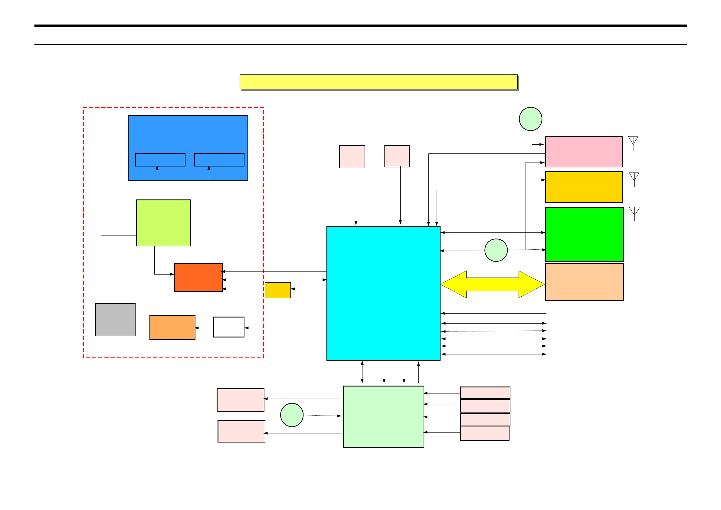
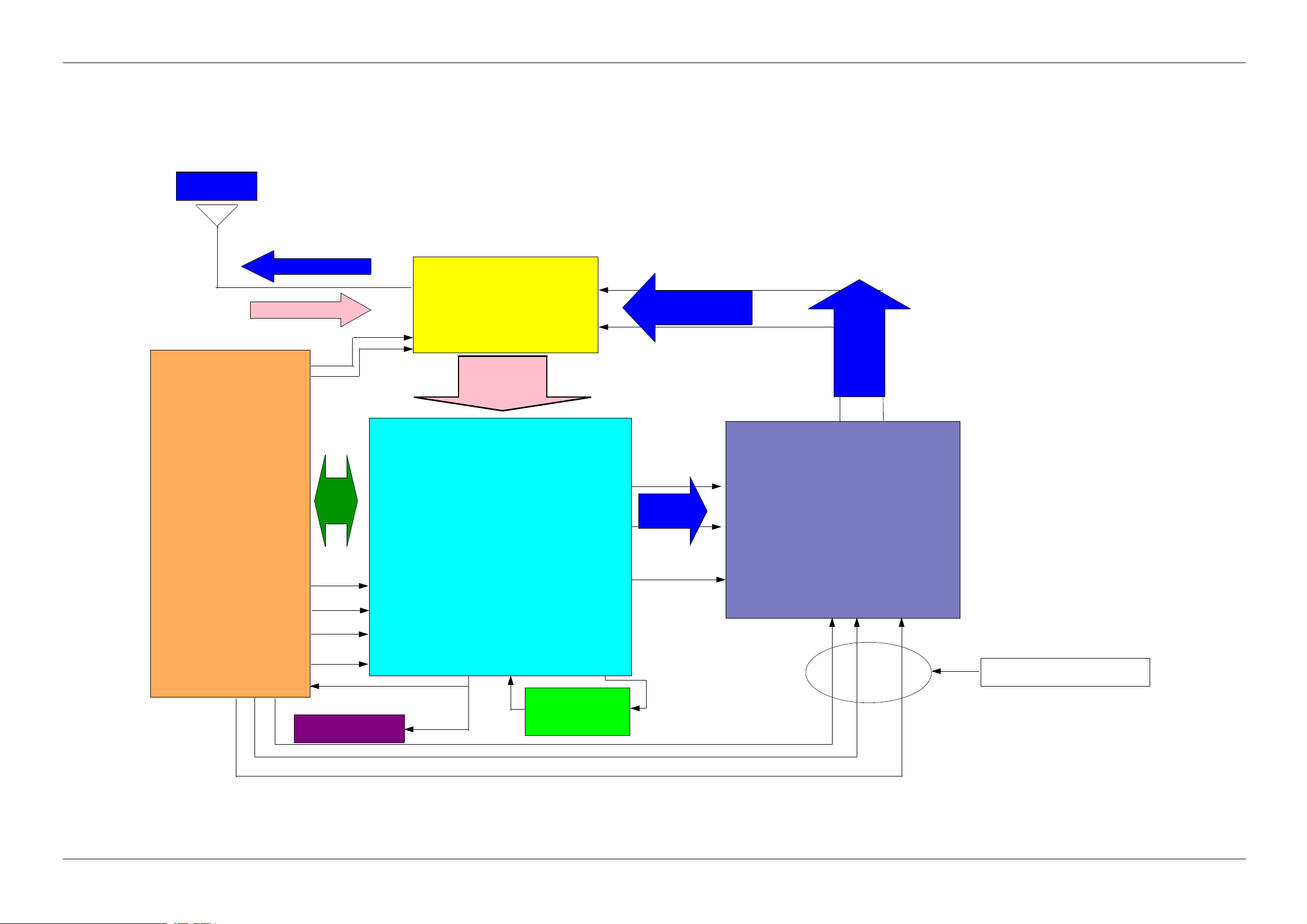
Block Diagrams
7.
7-1.
Block Diagram
LED+
Main TFT LCD
(2.2",
LED5EA
RN5T652
LED Driver IC,
(
DUAL LDO)
QVGA
)
LCD PartBLU
16
RGB I/F
bit
GT-S5200 Block Diagram
Ear
MIC
7
MIC_P
MIC_N
Main
MIC
/
EARMICP
EARMICN
PNX651
PCM/UART
IIC/ANL, ANR
TX_RX I/Q
MHz
26
KHz
32
BLUETOOTH
CM2070
(B
FM RADIO
TEA5990)
(
RF BLOCK
PAM(RF3159G)
Transceiver(QS1001
FEM(HWXR874-1)
)
VDD_CAM_CORE_1.8V
+
VDD_CAM_AF_3.0V
+
FLASH
LED
MOTOR
CAMERA
M,CMOS)
(3
VDD_CAM_IO_1.8V
LDO
Earphone
SPK/RCV
YUV,8bit
I2C
LDO
MOTOR_EN
EARSPK_R
EARSPK_L
32
KHz
SPK_P
SPK_N
CAM_EN
ARM946
GSM/GPRS/EDGE
BASEBAND Processor
Saturn DSP Core
I2C
EAR1
EAR2
HFR_P
HFR_N
MAX8699
LDO, DC/DC,Sim I/F
CHG IC, RTC, On_key,
OVP IC
PWR
BUS
Battery
SIM
Backup BAT
TA, USB
MEMORY
KAP29WN00C-AEEC
256M/1
KEY PBA
T-FLASH
ETM
JTAG
I/O con.
SIM
G/256M
7-1
SAMSUNG Proprietary-Contents may change without notice
This Document can not be used without Samsung's authorization
Page 25
Block Diagrams
TRANSCEIVER
QS1001
GSM/GPRS/EDGE
FEM
HWXR874
QUADBAND
RX LINE
PNX6517
ARM946
GSM/GPRS/EDGE
IQ
ANTENNA
RX LINE
VC1
VC2
IN
IP
QN
QP
I-
I+
Q-
Q+
RF_EN
RF_CLK
RF_DATA
PAM
SKY77344
GSM_IN
DCS_IN
DPCS_TX
GSM_TX
TX
LINE
TX LINE
TX LINE
26MHz
REF_CLK(26MHz)
RAMP
PON_PA(PAM_EN)
BAND_SEL
MODE_SEL
RAMP_OUT
BT_CLK(26MHz)
PAM CONTROL SIGNAL
REF_OUT
TX LINE
7-2.
RF Blcok Diagram
7-2
SAMSUNG Proprietary-Contents may change without notice
This Document can not be used without Samsung's authorization
Page 26
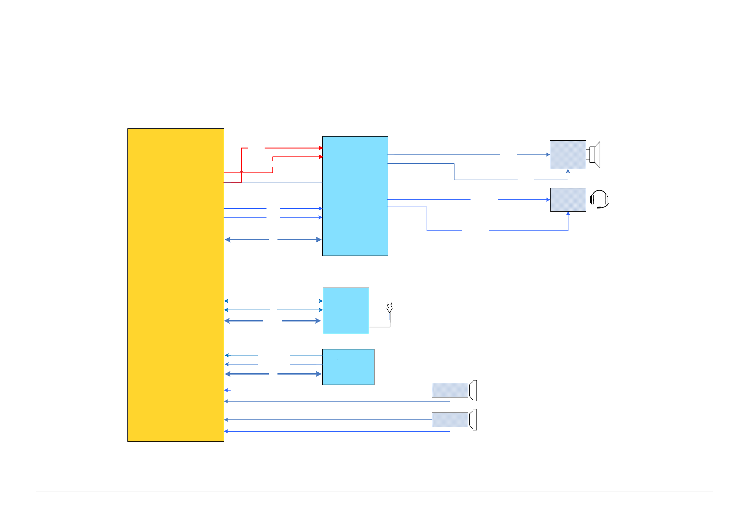
Block Diagrams
7-3.
Audio Block Diagram
HFR1
HFR2
EAR1
EAR2
HFR_N
SDA / SDL
HFR_P
EAR1
EAR2
I2C
RXINN
RXINP
INA1
INA2
INB1
INB2
MAX8699
OUTP
OUTN
HPR
HPL
EARSPK_R
EARSPK_L
SPK_P
2008.11.24 by ssimar
SPEAKER
SPK_N
EARPHONE
Main Chip
(PNX6517)
DU
DD
ANL
ANR
MICP
MICN
AUXMICP
AUXMICN
DU
DD
UART2
TXD2/RXD2
FM_RADIO_L
FM_RADIO_R
I2C
SDA / SDL
PCM_OUT
PCM_IN
BC6
AUDOL
AUDOR
TEA5991
BT_ANT
MAIN MIC
EAR MIC
7-3
SAMSUNG Proprietary-Contents may change without notice
This Document can not be used without Samsung's authorization
Page 27
PCB Diagrams
8.
Main top view]
[
TAC500 TAC501
ZD503
TP_HD_ZERO
ZD504
TP_TDI
CN200
R318
C334
R507
F500F501F502 F503F504
F505F506
R506
C216
C415
C410
C411
TP_PMU_INT
F401
C335
C403
L402
C401C402
L401
C325
L300
C338
C211
U302
BOTH_HOLE_201BOTH_HOLE_202
C341
L301
ZD502
C510
ZD505
C505
C340
R206
U301
R317
C339
C413
R416
C407
R409
C409
C414
C412
ZD403
R400
F400
R408
ZD400
C400
L400
SW500
C418
C417
R417R420
IFC400
C503
R503
TP_TCK
TP_TDO
L500
U500
C502
TP_BEn
TP_WEn
TP_EXT
C204
C201
ZD402
R402
R403
ZD405
R413
R404R405
ZD404
R401
BOTH_HOLE_200
C508
R502
R504
R411
R406
C416
C509
R309
C329
C324
C333
C302
C314
C309
C311
C307
C332
C308
C303
C315
C326
C306
C328
BTC500
TP_TRST
ZD201
TP_TMS
TP_CSn_RAM
TP_HA_ONE TP_HA_ZERO
BOTH_HOLE_203
TP_RTCK
C500
C511
TP_CS_NAND
TP_OEn
ZD500
R207
C200
TP_CS_FLASH
C202
TP_WAITn
UME200
CN400
C217
C337
OSC300
C506
UCP200
C318
U300
C331
C203
R311
TP_LD_ONE
HDC501
F507
C321
C322
R312
C317
R313
R300
C323
C330
R307
R308
R315
C336
R316
MIC400
8-1
SAMSUNG Proprietary-Contents may change without notice
This Document can not be used without Samsung's authorization
Page 28

PCB Diagrams
Main Bottom view]
[
ZD501
TP_RF_EN
TP_RF_DATA
TP_RF_CLK
SIM300
R500
C313
VR500
C504
R303
R304
C312
R501 R505
C501
BAT300
HDC500
F100
SC108
C132C133
C130
OSC100
U100
L104
L106
C107
C108
C110
C113
C117
C101
SC106
C139
L105
C114
C140
PAM100
C104
C103
C145
R103
C124
SC101
C100
SC103
L112
C111
C342
C316
C220
R310
C320
R415
R414
C404
C405
C406
C408
TP_DIGIT
SC105
R201
R202
C131
U400
C134
C141
C135
SC110
ANT102
C300
C146
C207
C213
C343
C304
C126
R107
U101
F101
L103
C310
R105
C144
C127
C136
C205
C214
ZD200
L111
C218
C210
TP_TXD_TWO
C305
C301
RFS100
C105
C109
C112
R100
C138
C137
C129
SC102
C122C123
TP_RAMP
L107L108
C118
C119
C120
C106
L101
ANT100 ANT101
8-2
SAMSUNG Proprietary-Contents may change without notice
This Document can not be used without Samsung's authorization
Page 29

9. Flow Chart of Troubleshooting
Power On
9-1.
Power On'does not work
'
Yes
Check the Battery Voltage
is more than
VISA
C326(
Check the Clock at
OSC300
C303(+VDD_IO_LOW)
VDD_IO_HIGH)="H"?
C308(+
3.4V
Yes
)=2.7
Yes
KHZ
=32
Yes
Yes
V?
No
No
No
&
No
Change the Battery
Check the PMU related to VINT
Resolder OSC
Check the related circuit
300
VDD_GSM_CORE_1V2)
C338(
V?
=1.2
Yes
Check for the clock at
MHz
=26
Yes
Check the initial operation
Yes
END
SAMSUNG Proprietary-Contents may change without notice
This Document can not be used without Samsung's authorization
C130
9-1
No
No
Check the+VDD_GSM_CORE circuit
Check the clock generation circuit
related to
(
U100)
Page 30

Flow Chart of Troubleshooting
V_EXT_CHARGE_5V0
C328
OSC300
C331
HFR_P
HFR_N
EAR1
EAR2
SPK_N
SPK_P
5
0
0
1
5
0
0
1
VDD_MAINKEY_3V3
VDD_SD_3V3
VDD_SLEEP_2V9
VDD_IO_HIGH_2V9
VDD_USB_3V3
AUX_ON
JACK_IN
R315
R316
3
4
3
C
VDD_AUDIO_2V6
VDD_IO_LOW_1V8
VDD_PLL_1V2VDD_SUB_KEY_3V3
VDD_BAI_2V6
VDD_SYN_2V8
VDD_RX_TX_2V8
5
0
0
1
L300
5
0
0
1
5
0
0
1
R307
1005
R308
1005
R309
1005
SIMOFFn
VDD_SIM_3V0
DETECT_VBUS
1
BAT300
2
C336
1005
C338
C300
C302
1005
C304
1005
C306
C308
0
C310
5
0
0
1
MES_BATT
C312
C317
1005
C321
1005
C322
1005
R313
SHORT
R300
1005
SHORT
REF_ON_PMU
PMU_PWREN2
R303
1005
5
0
0
1
R304
C318
1005
1005
C323
C337
VBAT
C313
1
1
9
8
2
1
2
1
1
E
D
B
D
C
E
C
T
D
D
D
S
B
T
T
D
T
D
D
A
T
T
V
V
V
B
3
A
2
1
A
M2
B
D
B
D
D
IN1
C3
IN2
B4
IN3
B10
IN4
B8
IN5
K6
IN6
K12
IN7
L5
IN8
M10
IN9
J5
INA1
H6
INA2
J7
INB1
H8
INB2
K8
C1N
L9
C1P
H12
OUTN
L11
OUTP
F12
CHGIN
F10
CHGINB
H2
XIN
J1
XOUT
C9
PWREN1
E5
PWREN2
G9
TEST1
J9
TEST2
D
N
G
A
1
6
1
M
3
2
3
3
C
5
4
3
3
3
3
3
3
C
C
C
G
V
5
_
S
U
B
V
2
1
1
5
5
7
9
3
6
1
1
E
A
A
A
A
C
B
A
D
2
D
D
D
D
D
S
D
D
D
D
D
D
D
D
D
U
D
D
D
D
V
V
V
V
V
B
V
V
V
1
6
5
V
4
V
P
C
C
G3
IO
F
F
D
L
D
D
L
H
REC1B
R
R
G7
REC2B
M4
HPL
L3
HPR
F2
MICBIAS
R311
H10
RXINN
K10
RXINP
R312
F4
SIMOFFB
C7
SIMVCC
B12
USBLDO
U300
2
1
D
D
D
N
N
N
G
G
P
P
G
1
8
2
1
K
M
J
D10
VL
C325
K4
1005
VBIAS
G1
VISA
E3
VSAVE
H4
CLK32K
D4
IRQB
E7
SCL
D6
SDA
L1
LX
J3
FB
C329
F8
REFBP
F6
1005
ONKEYB
G5
RESETB
3
D
N
S
C
C
S
G
N
N
V
P
7
2
1
L
5
0
C330
0
1
C301
C303
C305
C307
C309
5
0
0
1
C311
C315
1005
HFR_N
1005
HFR_P
1005
C324
1005
C326
TP_PMU_INT
INT_PMU
SCL
ONKEY_N
RST_BB
C314
1005
32KHz_DIGIT
SDA
RX_TX_QN
RX_TX_QP
RX_TX_IN
RX_TX_IP
REF_ON_PMU
REF_CLK
BT_CLK
1005
L108
C120
1005
1005
1005
C130
0
1
9
2
3
4
5
6
7
8
2
1
1
1
1
1
1
1
1
1
-
-
-
-
2
+
+
+
+
X
X
X
X
X
F
X
X
X
X
T
R
R
R
R
_
R
R
R
R
R
_
_
_
_
_
_
S
_
_
_
S
S
M
M
D
S
S
C
M
M
C
C
S
S
P
D
C
C
S
S
|
P
D
G
G
V
P
D
G
S
G
S
E
NC
21
TEST_A
22
TEST_B
23
NC
24
NC
25
VDD_BB
26
Q-
27
Q+
28
I-
29
I+
30
US|EGSM_TX
E
S
C
U
U
D
PA_VCTRL
TX_VCTRL
VDD_RF
U100
VDD_LO
VCO_SYN_REG
VDD_SYN
VDD_IO
DATA
G
E
B
R
G
T
O
CLK
3
_
E
X
U
T
|1
G
-
+
R
C
I
U
O
N
6
_
_
D
D
O
2
IN
IN
E
O
_
P
_
_
_
_
_
_
D
X
F
F
F
F
D
D
K
M
N
E
L
E
C
E
E
D
D
E
E
L
R
C
V
G
R
T
D
R
R
V
1
0
3
1
7
6
5
4
2
8
9
4
4
3
3
3
3
3
3
3
3
3
5
0
0
1
C123
10
9
8
7
6
5
4
3
TP_RF_DATA
2
TP_RF_CLK
1
5
0
0
1
C129
TP_RF_EN
RF_EN
VDD_SYN_2V8
OSC100
5
0
0
1
5
0
43
1
C133
0
1
C132
2
TP_RAMP
RF_DATA
RF_CLK
5
0
0
1
C122
VDD_IO_LOW_1V8
5
0
0
1
C137
VDD_IO_HIGH_2V9
5
0
0
1
C138
R103
RAMP_OUT
5
RAMP
0
0
1
C124
9-2
SAMSUNG Proprietary-Contents may change without notice
This Document can not be used without Samsung's authorization
Page 31

Flow Chart of Troubleshooting
9-3
SAMSUNG Proprietary-Contents may change without notice
This Document can not be used without Samsung's authorization
Page 32

Flow Chart of Troubleshooting
Initial
9-2.
Initial Failure
CP200 RSTON
U
TP_RSTON) is"High"?
(
Yes
CP200RSTEXTn
U
TP_EXT) is"High"?
(
Yes
Check the16bit data signal
memory CE
&
END
Yes
No
No
Check the circuit related to reset
CheckUCP
or change the PBA
200
9-4
SAMSUNG Proprietary-Contents may change without notice
This Document can not be used without Samsung's authorization
Page 33

Flow Chart of Troubleshooting
9-5
SAMSUNG Proprietary-Contents may change without notice
This Document can not be used without Samsung's authorization
Page 34

Flow Chart of Troubleshooting
Charging Part
9-3.
Abnormal charging part
Yes
Check the C337
>4.9V
Yes
TP_AUX_ON
Low"?
="
Yes
END
No
No
Check the circuit related to
V_EXT_CHARGE
Check the circuit related to
AUX_ON signal
9-6
SAMSUNG Proprietary-Contents may change without notice
This Document can not be used without Samsung's authorization
Page 35

Flow Chart of Troubleshooting
V_EXT_CHARGE_5V0
C328
OSC300
C331
HFR_P
HFR_N
EAR1
EAR2
SPK_N
SPK_P
5
0
0
1
5
0
0
1
VDD_MAINKEY_3V3
VDD_SD_3V3
VDD_SLEEP_2V9
VDD_IO_HIGH_2V9
VDD_USB_3V3
AUX_ON
JACK_IN
R315
R316
3
4
3
C
VDD_AUDIO_2V6
VDD_IO_LOW_1V8
VDD_PLL_1V2VDD_SUB_KEY_3V3
VDD_BAI_2V6
VDD_SYN_2V8
VDD_RX_TX_2V8
5
0
0
1
L300
5
0
0
1
5
0
0
1
R307
1005
R308
1005
R309
1005
SIMOFFn
VDD_SIM_3V0
DETECT_VBUS
1
BAT300
2
C336
1005
C338
C300
C302
1005
C304
1005
C306
C308
0
C310
5
0
0
1
MES_BATT
C312
C317
1005
C321
1005
C322
1005
R313
SHORT
R300
1005
SHORT
REF_ON_PMU
PMU_PWREN2
R303
1005
5
0
0
1
R304
C318
1005
1005
C323
C337
VBAT
C313
1
1
9
8
2
1
2
1
1
E
D
B
D
C
E
C
T
D
D
D
S
B
T
T
D
T
D
D
A
T
T
V
V
V
B
3
A
2
1
A
M2
B
D
B
D
D
IN1
C3
IN2
B4
IN3
B10
IN4
B8
IN5
K6
IN6
K12
IN7
L5
IN8
M10
IN9
J5
INA1
H6
INA2
J7
INB1
H8
INB2
K8
C1N
L9
C1P
H12
OUTN
L11
OUTP
F12
CHGIN
F10
CHGINB
H2
XIN
J1
XOUT
C9
PWREN1
E5
PWREN2
G9
TEST1
J9
TEST2
D
N
G
A
1
6
1
M
3
2
3
3
C
5
4
3
3
3
3
3
3
C
C
C
G
V
5
_
S
U
B
V
2
1
1
5
5
7
9
3
6
1
1
E
A
A
A
A
C
B
A
D
2
D
D
D
D
D
S
D
D
D
D
D
D
D
D
D
U
D
D
D
D
V
V
V
V
V
B
V
V
V
1
6
5
V
4
V
P
C
C
G3
IO
F
F
D
L
D
D
L
H
REC1B
R
R
G7
REC2B
M4
HPL
L3
HPR
F2
MICBIAS
R311
H10
RXINN
K10
RXINP
R312
F4
SIMOFFB
C7
SIMVCC
B12
USBLDO
U300
2
1
D
D
D
N
N
N
G
G
P
P
G
1
8
2
1
K
M
J
D10
VL
C325
K4
1005
VBIAS
G1
VISA
E3
VSAVE
H4
CLK32K
D4
IRQB
E7
SCL
D6
SDA
L1
LX
J3
FB
C329
F8
REFBP
F6
1005
ONKEYB
G5
RESETB
3
D
N
S
C
C
S
G
N
N
V
P
7
2
1
L
5
0
C330
0
1
C301
C303
C305
C307
C309
5
0
0
1
C311
C315
1005
HFR_N
1005
HFR_P
1005
C324
1005
C326
TP_PMU_INT
INT_PMU
SCL
ONKEY_N
RST_BB
C314
1005
32KHz_DIGIT
SDA
9-7
SAMSUNG Proprietary-Contents may change without notice
This Document can not be used without Samsung's authorization
Page 36

Flow Chart of Troubleshooting
Sim Part
9-4.
Phone can't access SIM Card
SIM
SIM
300
After SIM card inserted,
SIM
300
pin1is"High"?
300
pin3(SIMCLK)is working?
pin2(SIMRST) is"High"?
Check the SIM Card
Check the circuit related to SIM300
No
Check the UCP200 or Change the PBA
Yes
No
Check the UCP200 or Change the PBA
Yes
Yes
END
9-8
SAMSUNG Proprietary-Contents may change without notice
This Document can not be used without Samsung's authorization
Page 37

SIM_RST
C342
VDD_SIM_3V0
5
5
0
0
0
0
1
1
C320
SIM300
5000-6P-1.9S
11
22
6
5
33 4
7
7
8
8
9
9
G
16
11 11
10 10
14GG15
G
13
Flow Chart of Troubleshooting
5
0
0
1
R310
6
5
4
5
1212
0
0
C316
1
SIM_IOSIM_CLK
9-9
SAMSUNG Proprietary-Contents may change without notice
This Document can not be used without Samsung's authorization
Page 38

Flow Chart of Troubleshooting
Microphone Part
9-5.
Microphone does not work
Check the MIC connection
Yes
No
Resolder MIC
Yes
Check the circuit
fromUCP
Check F400 PIN4(JACK_IN)
is'High'
MIC is working?
200
END
to MIC
Yes
?
Yes
Yes
No
No
No
Resolder the C410, C413, C415
Check the JACK_INsignal
Replace the MIC
9-10
SAMSUNG Proprietary-Contents may change without notice
This Document can not be used without Samsung's authorization
Page 39

MIC_P
MIC_N
C415
M_GND
1005
C410
1005
C413
MIC_BIAS_2V15
5
0
0
1
Flow Chart of Troubleshooting
M_GND M_GND
MIC400
1
POWER
POWER
GND2GND1
3
GND
GND2
4
OUT
OUT
MIC Closed
9-11
SAMSUNG Proprietary-Contents may change without notice
This Document can not be used without Samsung's authorization
Page 40

Flow Chart of Troubleshooting
Speaker Part(Melody)
9-6.
Speaker does not work
R313, R300 are short?
Check the HDC501pin3,
pin4?
Yes
No
Resolder R313 and R300
Yes
No
Resolder HDC501
Yes
Speaker is working?
Yes
END
No
Change the Speaker
9-12
SAMSUNG Proprietary-Contents may change without notice
This Document can not be used without Samsung's authorization
Page 41

Flow Chart of Troubleshooting
V_EXT_CHARGE_5V0
C328
OSC300
C331
HFR_P
HFR_N
EAR1
EAR2
SPK_N
SPK_P
5
0
0
1
5
0
0
1
VDD_MAINKEY_3V3
VDD_SD_3V3
VDD_SLEEP_2V9
VDD_IO_HIGH_2V9
VDD_USB_3V3
AUX_ON
JACK_IN
R315
R316
3
4
3
C
VDD_AUDIO_2V6
VDD_IO_LOW_1V8
VDD_PLL_1V2VDD_SUB_KEY_3V3
VDD_BAI_2V6
VDD_SYN_2V8
VDD_RX_TX_2V8
5
0
0
1
L300
5
0
0
1
5
0
0
1
R307
1005
R308
1005
R309
1005
SIMOFFn
VDD_SIM_3V0
DETECT_VBUS
1
BAT300
2
C336
1005
C338
C300
C302
1005
C304
1005
C306
C308
0
C310
5
0
0
1
MES_BATT
C312
C317
1005
C321
1005
C322
1005
R313
SHORT
R300
1005
SHORT
REF_ON_PMU
PMU_PWREN2
R303
1005
5
0
0
1
R304
C318
1005
1005
C323
C337
VBAT
C313
1
1
9
8
2
1
2
1
1
E
D
B
D
C
E
C
T
D
D
D
S
B
T
T
D
T
D
D
A
T
T
V
V
V
B
3
A
2
1
A
M2
B
D
B
D
D
IN1
C3
IN2
B4
IN3
B10
IN4
B8
IN5
K6
IN6
K12
IN7
L5
IN8
M10
IN9
J5
INA1
H6
INA2
J7
INB1
H8
INB2
K8
C1N
L9
C1P
H12
OUTN
L11
OUTP
F12
CHGIN
F10
CHGINB
H2
XIN
J1
XOUT
C9
PWREN1
E5
PWREN2
G9
TEST1
J9
TEST2
D
N
G
A
1
6
1
M
3
2
3
3
C
5
4
3
3
3
3
3
3
C
C
C
G
V
5
_
S
U
B
V
2
1
1
5
5
7
9
3
6
1
1
E
A
A
A
A
C
B
A
D
2
D
D
D
D
D
S
D
D
D
D
D
D
D
D
D
U
D
D
D
D
V
V
V
V
V
B
V
V
V
1
6
5
V
4
V
P
C
C
G3
IO
F
F
D
L
D
D
L
H
REC1B
R
R
G7
REC2B
M4
HPL
L3
HPR
F2
MICBIAS
R311
H10
RXINN
K10
RXINP
R312
F4
SIMOFFB
C7
SIMVCC
B12
USBLDO
U300
2
1
D
D
D
N
N
N
G
G
P
P
G
1
8
2
1
K
M
J
D10
VL
C325
K4
1005
VBIAS
G1
VISA
E3
VSAVE
H4
CLK32K
D4
IRQB
E7
SCL
D6
SDA
L1
LX
J3
FB
C329
F8
REFBP
F6
1005
ONKEYB
G5
RESETB
3
D
N
S
C
C
S
G
N
N
V
P
7
2
1
L
5
0
C330
0
1
C301
C303
C305
C307
C309
5
0
0
1
C311
C315
1005
HFR_N
1005
HFR_P
1005
C324
1005
C326
TP_PMU_INT
INT_PMU
SCL
ONKEY_N
RST_BB
C314
1005
32KHz_DIGIT
SDA
RST_LCD
EN_CAM_PWR
LD_SUB(0)
LD_SUB(2)
LD_SUB(4)
LD_SUB(6)
LD_SUB(8)
LD_SUB(10)
LD_SUB(12)
LD_SUB(14)
LD_SUB(7)
LD_SUB(5)
LD_SUB(3)
LD_SUB(1)
LD_SUB(15)
LD_SUB(13)
LD_SUB(11)
LD_SUB(9)
LCD_RS_SUB
LCD_CS_SUB
LCD_WR_SUB
FLM_SUB
FLASH_M
KEY_COL(2)
KEY_COL(4)
KEY_ROW(4)
KEY_ROW(3)
KEY_ROW(2)
TP_LD_ONE
VDD_VIB_3V3
VDD_IO_HIGH_2V9
60
54
50
40
38
36
34
32
30
24
22
20
18
16
14
12
10
8
6
4
2
HDC501
VDD_SUB_KEY_3V3
63
64
6162
C
C
C
C
N
N
N
N
60
59
59
57
58
5758
55
56
5556
54
53
53
51
52
5152
49
50
49
47
48
4748
45
46
4546
43
44
4344
41
42
4142
40
39
39
3738
37
3536
35
3334
33
32
31
31
29
30
29
27
28
2728
25
26
2526
2324
23
2122
21
19
20
19
17
18
17
1516
15
1314
13
1112
11
9
10
9
78
7
6
5
5
4
3
3
1
2
1
5
0
0
1
C505
C506
BLM15BA220SN1DR506
BLM15BA220SN1DR507
5
0
0
1
5
0
C508
5
D
Z
EN_CAM_AF_3V0
LCD_RD_SUB
Y_SUB(0)
Y_SUB(1)
Y_SUB(2)
Y_SUB(3)
Y_SUB(4)
Y_SUB(5)
Y_SUB(6)
Y_SUB(7)
CAM_PCLK_IN
CAM_MCLK_OUT
HSYNC_SUB
VSYNC_SUB
RST_CAM
FLASH_P
EN_LCD_BL
ONKEY_N
CAM_SDA_SUB
CAM_SCL_SUB
KEY_COL(3)
SPK_P
SPK_N
5
0
0
1
C509
VBAT
C510
9-13
SAMSUNG Proprietary-Contents may change without notice
This Document can not be used without Samsung's authorization
Page 42

Flow Chart of Troubleshooting
9-14
SAMSUNG Proprietary-Contents may change without notice
This Document can not be used without Samsung's authorization
Page 43

Key Data Input
9-7.
Check Initial Operation
Yes
When one of the keys is
pressed,
is it displayed on LCD?
Yes
No
Flow Chart of Troubleshooting
Check the Dome sheet or
the KeyPBA connection with HDC50
0
When one of the keys is
pressed,
KBIO signal is OK?
Yes
END
No
Replace the PBA
9-15
SAMSUNG Proprietary-Contents may change without notice
This Document can not be used without Samsung's authorization
Page 44

Flow Chart of Troubleshooting
KEY_ROW(0)
KEY_ROW(1)
KEY_ROW(2)
KEY_ROW(3)
KEY_ROW(4)
VDD_MAINKEY_3V3
123456
13
HDC500
11
3344
5566
7788
99
1111
131414
151516
22
KEY_COL(4)
1010
1212
16
KEY_COL(3)
KEY_COL(2)
KEY_COL(1)
KEY_COL(0)
ZD501
PESD5V0L5UV
9-16
SAMSUNG Proprietary-Contents may change without notice
This Document can not be used without Samsung's authorization
Page 45

Back Light(for Color Main LCD)
9-8.
Backlight does not work
Yes
Is LCD Contrast set on high
level in the Menu?
Yes
The HDC501 connected
correctly?
Flow Chart of Troubleshooting
No
Set LCD Contrast on high level
No
Reconnet correctly
HDC501 PIN
High
'
Is Backlight working
END
55,
Yes
'?
Yes
Yes
PIN57is
?
No
No
Change the main PBA
Change the LCD
9-17
SAMSUNG Proprietary-Contents may change without notice
This Document can not be used without Samsung's authorization
Page 46

Flow Chart of Troubleshooting
VDD_VIB_3V3
VDD_IO_HIGH_2V9
RST_LCD
EN_CAM_PWR
LD_SUB(0)
LD_SUB(2)
LD_SUB(4)
LD_SUB(6)
LD_SUB(8)
LD_SUB(10)
LD_SUB(12)
LD_SUB(14)
LD_SUB(7)
LD_SUB(5)
LD_SUB(3)
LD_SUB(1)
LD_SUB(15)
LD_SUB(13)
LD_SUB(11)
LD_SUB(9)
LCD_RS_SUB
LCD_CS_SUB
LCD_WR_SUB
FLM_SUB
FLASH_M
KEY_COL(2)
KEY_COL(4)
KEY_ROW(4)
KEY_ROW(3)
KEY_ROW(2)
TP_LD_ONE
60
54
50
40
38
36
34
32
30
24
22
20
18
16
14
12
10
8
6
4
2
HDC501
VDD_SUB_KEY_3V3
63
64
6162
C
C
C
C
N
N
N
N
59
60
59
57
58
5758
55
56
5556
54
53
53
51
52
5152
49
50
49
47
48
4748
45
46
4546
43
44
4344
41
42
4142
40
39
39
3738
37
3536
35
3334
33
32
31
31
29
30
29
27
28
2728
25
26
2526
2324
23
2122
21
19
20
19
17
18
17
1516
15
1314
13
1112
11
9
10
9
78
7
5
6
5
4
3
3
1
2
1
C505
5
0
0
1
C506
BLM15BA220SN1DR506
BLM15BA220SN1DR507
5
0
0
1
C508
5
0
0
1
5
0
5
D
Z
C509
EN_CAM_AF_3V0
LCD_RD_SUB
Y_SUB(0)
Y_SUB(1)
Y_SUB(2)
Y_SUB(3)
Y_SUB(4)
Y_SUB(5)
Y_SUB(6)
Y_SUB(7)
CAM_PCLK_IN
CAM_MCLK_OUT
HSYNC_SUB
VSYNC_SUB
RST_CAM
FLASH_P
EN_LCD_BL
ONKEY_N
CAM_SDA_SUB
CAM_SCL_SUB
KEY_COL(3)
SPK_P
SPK_N
VBAT
C510
9-18
SAMSUNG Proprietary-Contents may change without notice
This Document can not be used without Samsung's authorization
Page 47

Key Back Light
9-9.
Flow Chart of Troubleshooting
Main Key LED does not work
Yes
HDC500 pin7is"High"?
Yes
C300
=3.3V?
Yes
Is KeyPBA working
Yes
END
No
No
No
?
Check the
U300
Resolder or Change
Change the keyPBA
related to"VDD_KEY"
U300
9-19
SAMSUNG Proprietary-Contents may change without notice
This Document can not be used without Samsung's authorization
Page 48

Flow Chart of Troubleshooting
V_EXT_CHARGE_5V0
C328
OSC300
C331
VDD_MAINKEY_3V3
HFR_P
HFR_N
EAR1
EAR2
SPK_N
SPK_P
5
0
0
1
5
0
0
1
VDD_SD_3V3
VDD_SLEEP_2V9
VDD_IO_HIGH_2V9
VDD_USB_3V3
AUX_ON
JACK_IN
R315
R316
3
4
3
C
VDD_AUDIO_2V6
VDD_IO_LOW_1V8
VDD_PLL_1V2VDD_SUB_KEY_3V3
VDD_BAI_2V6
VDD_SYN_2V8
VDD_RX_TX_2V8
5
0
0
1
L300
5
0
0
1
5
0
0
1
R307
1005
R308
1005
R309
1005
SIMOFFn
VDD_SIM_3V0
DETECT_VBUS
1
BAT300
2
C336
1005
C338
C300
C302
1005
C304
1005
C306
C308
0
C310
5
0
0
1
MES_BATT
C312
C317
1005
C321
1005
C322
1005
R313
SHORT
R300
1005
SHORT
REF_ON_PMU
PMU_PWREN2
R303
1005
5
0
0
1
R304
C318
1005
1005
C323
C337
VBAT
C313
1
1
9
8
2
1
2
1
1
E
D
D
C
B
E
C
T
D
D
D
D
S
B
T
T
T
D
D
D
D
A
T
T
V
V
V
V
B
A
3
2
1
4
A
M2
B
D
B
D
D
D
IN1
C3
IN2
B4
IN3
B10
IN4
B8
IN5
K6
IN6
K12
IN7
L5
IN8
M10
IN9
J5
INA1
H6
INA2
J7
INB1
H8
INB2
K8
C1N
L9
C1P
H12
OUTN
L11
OUTP
F12
CHGIN
F10
CHGINB
H2
XIN
J1
XOUT
C9
PWREN1
E5
PWREN2
G9
TEST1
J9
TEST2
D
D
N
N
G
A
G
1
6
1
M
3
2
3
3
C
5
4
3
3
3
3
3
3
C
C
C
G
V
5
_
S
U
B
V
2
1
1
5
5
7
9
3
6
1
1
E
A
A
A
A
C
B
D
A
2
D
D
D
S
D
D
D
D
D
D
D
U
D
D
D
D
D
D
V
V
V
B
V
V
V
V
1
6
V
5
V
P
C
C
G3
IO
F
F
D
L
D
L
H
REC1B
R
R
G7
REC2B
M4
HPL
L3
HPR
F2
MICBIAS
R311
H10
RXINN
K10
RXINP
R312
F4
SIMOFFB
C7
SIMVCC
B12
USBLDO
U300
2
1
D
D
N
N
G
G
P
P
1
8
2
1
K
M
J
D10
VL
C325
K4
1005
VBIAS
G1
VISA
E3
VSAVE
H4
CLK32K
D4
IRQB
E7
SCL
D6
SDA
L1
LX
J3
FB
C329
F8
REFBP
F6
RESETB
1005
G5
ONKEYB
3
D
N
S
C
C
S
G
V
P
N
N
7
2
1
L
5
0
C330
0
1
C301
C303
C305
C307
C309
5
0
0
1
C311
C315
1005
HFR_N
1005
HFR_P
1005
C324
1005
C326
TP_PMU_INT
INT_PMU
SCL
ONKEY_N
RST_BB
C314
1005
32KHz_DIGIT
SDA
VDD_MAINKEY_3V3
HDC500
22
11
3344
13
5566
7788
99
1111
131414
151516
1010
1212
16
KEY_ROW(0)
KEY_ROW(1)
KEY_ROW(2)
KEY_ROW(3)
KEY_ROW(4)
123456
ZD501
PESD5V0L5UV
9-20
SAMSUNG Proprietary-Contents may change without notice
This Document can not be used without Samsung's authorization
KEY_COL(4)
KEY_COL(3)
KEY_COL(2)
KEY_COL(1)
KEY_COL(0)
Page 49

Flow Chart of Troubleshooting
9-21
SAMSUNG Proprietary-Contents may change without notice
This Document can not be used without Samsung's authorization
Page 50

Flow Chart of Troubleshooting
9-10.
Camera part
Camera" function does not work
"
Camera connected with
LCD module correctly?
Is the Camera working?
When camera Preview
mode operates, HDC501
PIN
54is'
Yes
Yes
Yes
High
No
No
No
'?
Reconnect the camera module
Change the camera module
Change the main PBA
Yes
Replace the LCD module
END
9-22
SAMSUNG Proprietary-Contents may change without notice
This Document can not be used without Samsung's authorization
Page 51

RST_LCD
EN_CAM_PWR
LD_SUB(0)
LD_SUB(2)
LD_SUB(4)
LD_SUB(6)
LD_SUB(8)
LD_SUB(10)
LD_SUB(12)
LD_SUB(14)
LD_SUB(7)
LD_SUB(5)
LD_SUB(3)
LD_SUB(1)
LD_SUB(15)
LD_SUB(13)
LD_SUB(11)
LD_SUB(9)
LCD_RS_SUB
LCD_CS_SUB
LCD_WR_SUB
FLM_SUB
FLASH_M
KEY_COL(2)
KEY_COL(4)
KEY_ROW(4)
KEY_ROW(3)
KEY_ROW(2)
TP_LD_ONE
60
54
50
40
38
36
34
32
30
24
22
20
18
16
14
12
10
8
6
4
2
HDC501
Flow Chart of Troubleshooting
VDD_VIB_3V3
VDD_IO_HIGH_2V9
VDD_SUB_KEY_3V3
63
64
6162
C
C
C
C
N
N
N
N
59
60
59
57
58
5758
55
56
5556
54
53
53
51
52
5152
49
50
49
47
48
4748
45
46
4546
43
44
4344
41
42
4142
39
40
39
3738
37
3536
35
3334
33
31
32
31
30
29
29
27
28
2728
25
26
2526
2324
23
2122
21
19
20
19
18
17
17
1516
15
1314
13
1112
11
10
9
9
78
7
6
5
5
3
4
3
2
1
1
5
0
0
1
C505
C506
BLM15BA220SN1DR506
BLM15BA220SN1DR507
5
0
0
1
C508
5
0
0
1
5
0
5
D
Z
EN_CAM_AF_3V0
LCD_RD_SUB
Y_SUB(0)
Y_SUB(1)
Y_SUB(2)
Y_SUB(3)
Y_SUB(4)
Y_SUB(5)
Y_SUB(6)
Y_SUB(7)
CAM_PCLK_IN
CAM_MCLK_OUT
HSYNC_SUB
VSYNC_SUB
RST_CAM
FLASH_P
EN_LCD_BL
ONKEY_N
CAM_SDA_SUB
CAM_SCL_SUB
KEY_COL(3)
SPK_P
SPK_N
C509
VBAT
C510
9-23
SAMSUNG Proprietary-Contents may change without notice
This Document can not be used without Samsung's authorization
Page 52

Flow Chart of Troubleshooting
9-11.
GSM850 Receiver
RF input:CH center freq
Cell Power
pin
pin
RX ON
:-60
Yes
F100 Pin11
dBm
-65
≥
Yes
U100
19≥-70
20≥-70
Yes
dBm
dBm
dBm
: +67.7
kHz
No
No
Resolder RFS100,C106,L10
Resolder F100, C1
07,C108,
1
L104
U100 pin
0.2
≥
Check UCP200
END
26,27,28,29
Vp_p
No
Yes
U100
pin5,10,11,25,32,34,
36≥2.8V
pin4
1.8V
≥
Yes
No
Check&Resolder
C1
32,C123,C122
and PMU Part
Resolder
U100
9-24
SAMSUNG Proprietary-Contents may change without notice
This Document can not be used without Samsung's authorization
Page 53

RFS100
C
2
1
Flow Chart of Troubleshooting
G
G
A
4
3
C105
C109
ANT100
1005
R100
C112
T
R
O
H
S
DPCS_TX
GSM_TX
ANT101
11
ANT
14
VC1
VC2
VC1
10
VC2
15
DCS|PCS-TX
17
EGSM|GSM850-TX
GG
9
12 13GG16
C106
GSM850-RX1
GSM850-RX2
18G19GG20
L101
F100
EGSM-RX1
EGSM-RX2
DCS-RX1
DCS-RX2
PCS-RX1
PCS-RX2
C107
1005
C108
L104
1005
1005
C110
1
2
3
4
5
6
7
8
C113
C117
C118
1005
L106
1005
1005
L107
1005
C119
RX_TX_QN
RX_TX_QP
RX_TX_IN
RX_TX_IP
REF_ON_PMU
1005
C120
1005
C107
1005
L104
C108
1005
1005
C110
1005
L106
C113
1005
C117
1005
L107
C118
1005
C119
1005
L108
C120
1005
1005
NC
21
TEST_A
22
TEST_B
23
NC
24
NC
25
VDD_BB
26
Q-
27
Q+
28
I-
29
I+
30
L108
1005
L105
1005
DPCS_IN
5
5
0
0
0
0
1
1
C123
5
0
0
1
C129
C114
TP_RF_DATA
TP_RF_CLK
C140
VDD_RX_TX_2V8
5
0
0
1
GSM_IN
TP_RAMP
RF_DATA
RF_CLK
5
0
0
1
C122
VDD_IO_LOW_1V8
5
0
0
1
C137
VDD_RX_TX_2V8
RAMP
R103
RAMP_OUT
5
0
0
1
C124
C139
8
7
6
5
4
3
9
0
2
1
1
1
1
1
1
1
1
2
1
1
-
-
-
-
+
+
2
+
+
X
R
_
M
S
G
S
U
N
E
_
K
L
C
1
3
X
X
X
X
X
F
X
X
X
T
R
R
R
R
_
R
R
R
R
_
_
_
_
_
_
_
_
S
S
S
M
M
D
S
S
C
M
C
C
S
S
D
P
C
C
S
|
P
D
G
G
V
P
D
G
S
E
S
US|EGSM_TX
E
C
U
D
10
PA_VCTRL
9
TX_VCTRL
8
VDD_RF
U100
B
O
3
X
T
|1
-
+
C
U
6
D
IN
2
IN
O
_
_
_
_
_
F
F
F
F
D
E
E
E
E
D
R
R
R
R
V
2
5
4
3
3
3
3
3
7
VDD_LO
6
VCO_SYN_REG
5
VDD_SYN
4
VDD_IO
3
DATA
G
E
2
R
T
G
CLK
_
E
U
1
R
IG
O
_
_
D
_
P
O
D
X
D
M
N
C
D
E
E
V
T
D
G
L
9
8
7
6
0
1
3
3
3
3
4
4
REF_CLK
1005
BT_CLK
C130
OSC100
43
1
5
0
0
1
C133
2
VDD_SYN_2V8
C132
TP_RF_EN
RF_EN
5
0
0
1
9-25
SAMSUNG Proprietary-Contents may change without notice
This Document can not be used without Samsung's authorization
VDD_IO_HIGH_2V9
5
0
0
1
C138
Page 54

Flow Chart of Troubleshooting
9-26
SAMSUNG Proprietary-Contents may change without notice
This Document can not be used without Samsung's authorization
Page 55

Flow Chart of Troubleshooting
9-12.
GSM850 Transmitter
TX ON(5Level)
Yes
F100 Pin11
dBm
30
≥
No
Check F100
pin14=H, pin10=L
Yes
PAM100 pin1
≥
30
dBm
No
3
Yes
Resolder RFS100,C106,L10
No
Check control circuit and
Resolder F100
Yes
Resolder C1
1
45,C103
Check pam100 pin
1,2,3,17,18,20
Yes
U100 pin
26,27,28,29
Vp_p
0.2
≥
No
Check UCP200
END
OK?
No
Resolder or Change PAM100
Check VBAT or PAM control signal
Yes
pin5,10,11,25,32,34,
pin4
U100
36≥2.8V
1.8V
≥
Yes
No
Check&Resolder
C1
32,C123,C122
and PMU Part
Resolder
U100
9-27
SAMSUNG Proprietary-Contents may change without notice
This Document can not be used without Samsung's authorization
Page 56

Flow Chart of Troubleshooting
RFS100
C
2
1
G
G
A
4
3
C105
C109
ANT100
ANT101
L101
T
R
O
H
S
R100
1005
C106
C112
GG
9
12 13GG16
GSM850-RX1
GSM850-RX2
18G19GG20
F100
EGSM-RX1
EGSM-RX2
DCS-RX1
DCS-RX2
PCS-RX1
PCS-RX2
1
2
3
4
5
6
7
8
DPCS_TX
GSM_TX
11
ANT
14
VC1
VC2
VC1
10
VC2
15
DCS|PCS-TX
17
EGSM|GSM850-TX
C107
C108
C110
C113
C117
C118
1005
L104
1005
1005
1005
L106
1005
1005
L107
1005
C119
RX_TX_QN
RX_TX_QP
RX_TX_IN
RX_TX_IP
REF_ON_PMU
REF_CLK
BT_CLK
1005
C120
1005
C107
1005
L104
C108
1005
1005
C110
1005
L106
C113
1005
C117
1005
L107
C118
1005
L105
1005
DPCS_IN
5
5
0
0
0
0
1
1
C140
C139
C114
GSM_IN
VDD_RX_TX_2V8
C119
1005
L108
C120
1005
1005
1005
C130
9
8
7
4
1
5
2
6
3
0
1
1
1
1
1
1
1
1
1
2
-
-
-
-
+
2
+
+
+
X
R
_
M
S
G
NC
S
U
21
TEST_A
22
TEST_B
23
NC
24
NC
25
VDD_BB
26
Q-
27
Q+
28
I-
29
I+
30
N
E
_
K
L
C
X
X
X
X
X
F
X
X
X
T
R
R
R
R
_
R
R
R
R
_
_
_
_
_
S
_
_
_
S
S
M
M
D
S
S
C
M
C
C
S
S
C
D
C
S
|P
P
D
G
V
P
G
D
G
S
S
E
US|EGSM_TX
E
C
U
D
PA_VCTRL
TX_VCTRL
VDD_RF
U100
VDD_LO
VCO_SYN_REG
VDD_SYN
VDD_IO
DATA
G
E
B
R
T
G
O
3
T
|1
U
6
2
O
_
_
F
F
E
E
R
R
2
1
3
3
3
3
CLK
_
E
U
X
G
-
+
R
I
C
O
_
_
D
D
IN
IN
P
O
_
_
_
_
D
X
D
F
F
D
M
N
C
E
E
D
D
E
E
D
V
T
R
G
R
V
L
8
7
6
9
5
1
0
4
3
3
3
3
3
4
4
3
5
0
0
1
C123
10
9
8
7
6
5
4
3
TP_RF_DATA
2
TP_RF_CLK
1
5
0
0
1
C129
TP_RF_EN
RF_EN
TP_RAMP
RF_DATA
RF_CLK
VDD_IO_LOW_1V8
VDD_IO_HIGH_2V9
VDD_SYN_2V8
L108
1005
VDD_RX_TX_2V8
5
0
0
1
C122
R103
RAMP_OUT
5
RAMP
0
0
1
C124
5
0
0
1
C137
5
0
0
1
C138
OSC100
43
1
5
0
0
1
5
0
C133
0
1
2
C132
9-28
SAMSUNG Proprietary-Contents may change without notice
This Document can not be used without Samsung's authorization
Page 57

RAMP_OUT
MODE_SEL
GSM_TX
DPCS_TX
1005
C101
1005
C104
C145
L112
Flow Chart of Troubleshooting
VBAT
C100
1005
C103
1005
13
1005
C111
1005
15
3
19
20
GSM_OUT
VRAMP
VDET
MODE
7
8
1
1
1
2
T
T
T
T
A
A
B
B
V
V
PAM100
D
D
D
D
D
D
N
N
N
N
N
N
G
G
G
G
G
G
1
2
6
4
1
1
1
1
1
2
5
GSM_IN
4
DCS|PCS_INDCS|PCS_OUT
1
BS
2
EN
D
D
D
D
N
N
N
N
G
G
G
G
9
6
0
7
8
1
GSM_IN
DPCS_IN
BAND_SEL
PON_PA
9-29
SAMSUNG Proprietary-Contents may change without notice
This Document can not be used without Samsung's authorization
Page 58

Flow Chart of Troubleshooting
9-13.
GSM900 Receiver
RF input:CH center freq
Cell Power
pin14=L, pin10=L
pin
pin
RX ON
:-60
Yes
F100 Pin11
dBm
-65
≥
Yes
Check F100
Yes
U100
17≥-70
18≥-70
Yes
dBm
dBm
dBm
: +67.7
kHz
No
No
Resolder RFS100,C106,L10
No
Check control circuit and
Resolder F100
Resolder F100, C1
10,C113,
1
L10
6
U100 pin
0.2
≥
Check UCP200
END
26,27,28,29
Vp_p
No
Yes
U100
pin5,10,11,25,32,34,
36≥2.8V
pin4
1.8V
≥
Yes
No
Check&Resolder
C1
32,C123,C122
and PMU Part
Resolder
U100
9-30
SAMSUNG Proprietary-Contents may change without notice
This Document can not be used without Samsung's authorization
Page 59

RFS100
C
1
Flow Chart of Troubleshooting
A
G
G
2
4
3
ANT100
C105
1005
C109
ANT101
T
R
O
H
S
R100
C112
14
VC1
10
VC2
15
DCS|PCS-TX
17
EGSM|GSM850-TX
DPCS_TX
GSM_TX
VC1
VC2
11
ANT
GG
9
12 13GG16
C106
18G19GG20
L101
F100
GSM850-RX1
GSM850-RX2
EGSM-RX1
EGSM-RX2
DCS-RX1
DCS-RX2
PCS-RX1
PCS-RX2
C107
1005
L104
C108
1005
1005
C110
1
2
3
4
5
6
7
8
1005
C113
L106
1005
C117
1005
C118
L107
1005
C119
1005
C120
L108
1005
1005
C107
1005
L104
C108
1005
1005
C110
1005
C113
L106
1005
C117
1005
L107
C118
1005
L105
1005
DPCS_IN
5
5
0
0
0
0
1
1
C114
C140
VDD_RX_TX_2V8
GSM_IN
VDD_RX_TX_2V8
C139
C119
RX_TX_QN
RX_TX_QP
RX_TX_IN
RX_TX_IP
1005
L108
C120
1005
1005
8
7
6
5
4
9
3
0
2
-
+
X
X
R
R
_
_
M
M
S
S
G
G
S
NC
S
U
U
21
TEST_A
22
TEST_B
23
NC
24
NC
25
VDD_BB
26
Q-
27
Q+
28
I-
29
B
I+
3
|1
30
N
6
2
E
_
_
F
K
E
L
R
C
1
3
1
2
1
1
1
1
1
1
1
1
1
-
-
-
2
+
+
+
X
X
X
X
F
X
X
X
T
R
R
R
_
R
R
R
R
_
_
_
_
_
_
S
_
S
S
M
D
S
S
C
M
C
C
S
C
D
C
P
S
|
P
D
G
V
P
D
G
S
E
US|EGSM_TX
E
C
D
PA_VCTRL
TX_VCTRL
VDD_RF
U100
VDD_LO
VCO_SYN_REG
VDD_SYN
VDD_IO
DATA
G
E
R
T
G
O
CLK
_
E
U
X
T
G
-
+
R
I
C
O
U
_
_
D
D
IN
IN
O
_
P
O
_
_
_
_
D
X
D
F
F
F
D
M
N
C
E
E
E
D
D
E
E
V
T
D
R
R
G
L
R
V
9
8
7
2
6
5
4
0
3
1
3
3
3
3
3
3
3
4
3
4
5
0
0
1
C123
10
9
8
7
6
5
4
3
TP_RF_DATA
2
TP_RF_CLK
1
5
0
0
1
C129
TP_RAMP
RF_DATA
RF_CLK
5
0
0
1
C122
VDD_IO_LOW_1V8
5
0
0
1
C137
R103
RAMP_OUT
5
RAMP
0
0
1
C124
REF_ON_PMU
REF_CLK
1005
BT_CLK
C130
OSC100
43
1
5
0
0
1
C133
2
VDD_SYN_2V8
C132
TP_RF_EN
RF_EN
5
0
0
1
9-31
SAMSUNG Proprietary-Contents may change without notice
This Document can not be used without Samsung's authorization
VDD_IO_HIGH_2V9
5
0
0
1
C138
Page 60

Flow Chart of Troubleshooting
9-32
SAMSUNG Proprietary-Contents may change without notice
This Document can not be used without Samsung's authorization
Page 61

Flow Chart of Troubleshooting
9-14.
GSM900 Transmitter
TX ON(5Level)
Yes
F100 Pin11
dBm
30
≥
No
Check F100
pin14=H, pin10=L
Yes
PAM100 pin12
dBm
30
≥
No
Yes
Resolder RFS100,C106,L10
No
Check control circuit and
Resolder F100
Yes
Resolder C1
1
45,C103
Check pam100 pin
1,2,3,17,18,20
Yes
U100 pin
26,27,28,29
Vp_p
0.2
≥
No
Check UCP200
END
OK?
No
Resolder or Change PAM100
Check VBAT or PAM control signal
Yes
pin5,10,11,25,32,34,
pin4
U100
36≥2.8V
1.8V
≥
Yes
No
Check&Resolder
C1
32,C123,C122
and PMU Part
Resolder
U100
9-33
SAMSUNG Proprietary-Contents may change without notice
This Document can not be used without Samsung's authorization
Page 62

Flow Chart of Troubleshooting
RFS100
C
1
A
G
G
2
4
3
C105
C109
ANT100
1005
R100
C112
T
R
O
H
S
DPCS_TX
GSM_TX
ANT101
11
ANT
14
VC1
VC2
VC1
10
VC2
15
DCS|PCS-TX
17
EGSM|GSM850-TX
GG
9
12 13GG16
C106
18G19GG20
L101
F100
GSM850-RX1
GSM850-RX2
EGSM-RX1
EGSM-RX2
DCS-RX1
DCS-RX2
PCS-RX1
PCS-RX2
C107
1005
C108
L104
1005
1005
C110
1
2
3
4
5
6
7
8
C113
C117
C118
1005
L106
1005
1005
L107
1005
C119
RX_TX_QN
RX_TX_QP
RX_TX_IN
RX_TX_IP
REF_ON_PMU
1005
C120
1005
C107
1005
L104
C108
1005
1005
C110
1005
C113
L106
1005
C117
1005
L107
C118
1005
L105
1005
5
5
0
0
0
0
1
1
C139
C140
C114
VDD_RX_TX_2V8
C119
1005
L108
C120
1005
1005
0
2
-
+
X
X
R
R
_
_
M
M
S
S
G
G
S
NC
S
U
U
21
TEST_A
22
TEST_B
23
NC
24
NC
25
VDD_BB
26
Q-
27
Q+
28
I-
29
B
I+
3
|1
30
N
6
2
E
_
_
F
K
E
L
R
C
1
3
1
2
6
3
9
4
5
7
8
1
1
1
1
1
1
1
1
1
-
-
-
2
+
+
+
X
X
X
X
F
X
X
X
T
R
R
R
_
R
R
R
R
_
_
_
_
S
_
_
_
S
S
M
D
S
S
C
M
C
C
S
D
C
C
S
|P
P
D
G
V
P
D
G
S
E
US|EGSM_TX
E
C
D
10
PA_VCTRL
TX_VCTRL
VDD_RF
U100
VDD_LO
VCO_SYN_REG
VDD_SYN
VDD_IO
DATA
G
E
R
G
T
O
X
T
C
U
D
O
_
_
F
D
E
D
R
V
3
2
3
3
CLK
_
E
U
G
+
-
R
I
O
_
_
D
IN
IN
O
P
_
_
_
D
X
F
F
D
M
N
E
E
C
D
E
E
G
L
R
R
T
D
V
1
0
4
5
7
6
8
9
4
4
3
3
3
3
3
3
5
0
0
1
C123
9
8
7
6
5
4
3
TP_RF_DATA
2
TP_RF_CLK
1
5
0
0
1
C129
DPCS_IN
GSM_IN
TP_RAMP
1005
RF_DATA
RF_CLK
L108
5
0
0
1
C122
VDD_IO_LOW_1V8
5
0
0
1
C137
VDD_RX_TX_2V8
RAMP
R103
RAMP_OUT
5
0
0
1
C124
REF_CLK
BT_CLK
1005
C130
TP_RF_EN
RF_EN
VDD_SYN_2V8
OSC100
43
1
5
0
0
1
5
0
C133
0
1
2
C132
VDD_IO_HIGH_2V9
5
0
0
1
C138
9-34
SAMSUNG Proprietary-Contents may change without notice
This Document can not be used without Samsung's authorization
Page 63

RAMP_OUT
MODE_SEL
GSM_TX
DPCS_TX
C101
1005
Flow Chart of Troubleshooting
VBAT
C100
1005
C145
L112
C104
1005
C103
1005
13
1005
C111
1005
GSM_OUT
15
3
VRAMP
19
VDET
20
MODE
D
N
G
7
8
1
1
1
2
T
T
T
T
A
A
B
B
V
V
PAM100
D
D
D
D
D
N
N
N
N
N
G
G
G
G
G
4
6
1
1
2
1
1
2
1
1
5
GSM_IN
4
DCS|PCS_INDCS|PCS_OUT
1
BS
2
EN
D
D
D
D
N
N
N
N
G
G
G
G
7
8
9
6
0
1
GSM_IN
DPCS_IN
BAND_SEL
PON_PA
9-35
SAMSUNG Proprietary-Contents may change without notice
This Document can not be used without Samsung's authorization
Page 64

Flow Chart of Troubleshooting
9-15.
DCS Receiver
RF input:CH center freq
Cell Power
pin14=L, pin10=L
pin
pin
RX ON
:-60
Yes
F100 Pin11
dBm
-65
≥
Yes
Check F100
Yes
U100
15≥-70
16≥-70
Yes
dBm
dBm
dBm
: +67.7
kHz
No
No
Resolder RFS100,C106,L10
No
Check control circuit and
Resolder F100
Resolder F100, C117,C1
18,
1
L10
7
U100 pin
0.2
≥
Check UCP200
END
26,27,28,29
Vp_p
No
Yes
U100
pin5,10,11,25,32,34,
36≥2.8V
pin4
1.8V
≥
Yes
No
Check&Resolder
C1
32,C123,C122
and PMU Part
Resolder
U100
9-36
SAMSUNG Proprietary-Contents may change without notice
This Document can not be used without Samsung's authorization
Page 65

RFS100
C
1
Flow Chart of Troubleshooting
G
G
A
4
3
2
C105
C109
RX_TX_QN
RX_TX_QP
RX_TX_IN
RX_TX_IP
REF_ON_PMU
ANT100
1005
ANT101
T
R
O
H
S
R100
C112
11
ANT
14
VC1
10
VC2
15
DCS|PCS-TX
17
EGSM|GSM850-TX
DPCS_TX
GSM_TX
VC1
VC2
GG
9
12 13GG16
C106
GSM850-RX1
GSM850-RX2
18G19GG20
L101
F100
EGSM-RX1
EGSM-RX2
DCS-RX1
DCS-RX2
PCS-RX1
PCS-RX2
C107
1005
L104
C108
1005
1005
C110
1
2
3
4
5
6
7
8
1005
C113
L106
1005
C117
1005
C118
L107
1005
C119
1005
C120
L108
1005
1005
C107
1005
L104
C108
1005
1005
C110
1005
C113
L106
1005
C117
1005
L107
C118
1005
L105
1005
5
0
0
1
C139
C114
C140
VDD_RX_TX_2V8
DPCS_IN
5
0
0
1
GSM_IN
VDD_RX_TX_2V8
C119
1005
L108
C120
1005
1005
9
0
1
2
-
+
X
X
R
R
_
_
M
M
S
S
G
G
S
NC
S
U
U
21
TEST_A
22
TEST_B
23
NC
24
NC
25
VDD_BB
26
Q-
27
Q+
28
I-
29
B
I+
3
|1
30
N
6
2
E
_
_
F
K
E
L
R
C
2
1
3
3
8
1
+
X
R
_
M
S
G
E
T
U
O
_
F
E
R
3
3
7
1
-
X
X
R
R
_
_
S
M
C
S
D
G
E
U100
O
X
+
C
D
IN
_
_
D
F
E
D
V
R
4
3
1
2
3
4
5
6
1
1
1
1
1
1
-
2
+
+
X
X
F
X
X
T
R
_
R
R
R
_
_
S
_
_
S
D
S
S
C
C
D
C
C
|P
P
V
P
D
S
US|EGSM_TX
C
D
10
PA_VCTRL
9
TX_VCTRL
8
VDD_RF
7
VDD_LO
6
VCO_SYN_REG
5
VDD_SYN
4
VDD_IO
3
DATA
G
E
2
R
T
G
CLK
_
E
U
G
IN
_
F
E
R
6
5
3
3
1
R
I
O
_
_
D
P
O
_
D
X
D
M
N
C
D
E
E
D
V
G
T
L
0
1
8
7
9
4
4
3
3
3
C123
5
0
0
1
C129
5
0
0
1
TP_RF_DATA
TP_RF_CLK
TP_RAMP
RF_DATA
RF_CLK
5
0
0
1
C122
VDD_IO_LOW_1V8
5
0
0
1
C137
RAMP
R103
RAMP_OUT
5
0
0
1
C124
REF_CLK
BT_CLK
1005
C130
TP_RF_EN
RF_EN
VDD_SYN_2V8
OSC100
43
1
5
0
0
1
5
0
C133
0
1
2
C132
VDD_IO_HIGH_2V9
5
0
0
1
C138
9-37
SAMSUNG Proprietary-Contents may change without notice
This Document can not be used without Samsung's authorization
Page 66

Flow Chart of Troubleshooting
9-38
SAMSUNG Proprietary-Contents may change without notice
This Document can not be used without Samsung's authorization
Page 67

Flow Chart of Troubleshooting
9-16.
DCS Transmitter
TX ON(5Level)
Yes
F100 Pin11
dBm
25
≥
No
Check F100
pin14=L, pin10=H
Yes
PAM100 pin
≥
25
dBm
No
15
Yes
Resolder RFS100,C106,L10
No
Check control circuit and
Resolder F100
Yes
Resolder C1
11,
L11
1
2
Check pam100 pin
1,2,3,17,18,20
Yes
U100 pin
26,27,28,29
Vp_p
0.2
≥
No
Check UCP200
END
OK?
No
Resolder or Change PAM100
Check VBAT or PAM control signal
Yes
pin5,10,11,25,32,34,
pin4
U100
36≥2.8V
1.8V
≥
Yes
No
Check&Resolder
C1
32,C123,C122
and PMU Part
Resolder
U100
9-39
SAMSUNG Proprietary-Contents may change without notice
This Document can not be used without Samsung's authorization
Page 68

Flow Chart of Troubleshooting
RFS100
C
1
A
G
G
2
4
3
RX_TX_QN
RX_TX_QP
RX_TX_IN
RX_TX_IP
REF_ON_PMU
ANT100
C105
1005
C109
ANT101
T
R
O
H
S
R100
C112
14
10
15
17
VC1
VC2
DCS|PCS-TX
EGSM|GSM850-TX
DPCS_TX
GSM_TX
VC1
VC2
L101
C106
F100
11
ANT
GG
9
18G19GG20
12 13GG16
GSM850-RX1
GSM850-RX2
EGSM-RX1
EGSM-RX2
DCS-RX1
DCS-RX2
PCS-RX1
PCS-RX2
1
2
3
4
5
6
7
8
C107
1005
L104
C108
1005
1005
C110
1005
C113
L106
1005
C117
1005
C118
L107
1005
C119
1005
C120
1005
L108
1005
C107
1005
L104
C108
1005
1005
C110
1005
C113
L106
1005
C117
1005
L107
C118
1005
L105
1005
C140
VDD_RX_TX_2V8
DPCS_IN
5
0
0
1
GSM_IN
VDD_RX_TX_2V8
5
0
0
1
C139
C114
C119
1005
L108
C120
1005
1005
0
2
+
X
R
_
M
S
G
NC
S
U
21
TEST_A
22
TEST_B
23
NC
24
NC
25
VDD_BB
26
Q-
27
Q+
28
I-
29
I+
30
N
E
_
K
L
C
1
3
1
2
3
4
5
6
7
9
8
1
1
1
1
1
1
1
1
1
-
-
-
-
2
+
+
+
X
X
X
X
X
F
X
X
X
T
R
R
R
R
_
R
R
R
R
_
_
_
_
_
S
_
_
_
S
S
M
M
D
S
S
C
M
C
C
S
S
P
D
C
C
S
|
P
D
V
G
G
P
D
G
S
S
E
US|EGSM_TX
E
C
U
D
PA_VCTRL
TX_VCTRL
VDD_RF
U100
VDD_LO
VCO_SYN_REG
VDD_SYN
VDD_IO
DATA
G
E
B
R
T
G
O
3
T
|1
U
6
O
2
_
_
F
F
E
E
R
R
3
2
3
3
CLK
_
E
X
U
G
+
-
R
C
I
O
_
_
D
D
IN
IN
_
O
_
P
_
_
D
X
D
F
F
D
M
N
E
E
C
D
D
E
E
R
V
L
R
G
D
V
T
4
5
0
6
1
8
7
9
3
3
4
3
4
3
3
3
5
0
0
1
C123
10
9
8
7
6
5
4
3
TP_RF_DATA
2
TP_RF_CLK
1
5
0
0
1
C129
TP_RAMP
RF_DATA
RF_CLK
5
0
0
1
C122
VDD_IO_LOW_1V8
5
0
0
1
C137
R103
RAMP_OUT
5
RAMP
0
0
1
C124
REF_CLK
BT_CLK
1005
C130
TP_RF_EN
RF_EN
VDD_SYN_2V8
OSC100
43
1
5
0
0
1
5
0
C133
0
1
2
C132
VDD_IO_HIGH_2V9
5
0
0
1
C138
9-40
SAMSUNG Proprietary-Contents may change without notice
This Document can not be used without Samsung's authorization
Page 69

Flow Chart of Troubleshooting
VBAT
RAMP_OUT
MODE_SEL
GSM_TX
DPCS_TX
1005
C101
1005
C104
C145
L112
1005
C103
1005
13
1005
C111
1005
GSM_OUT
15
3
VRAMP
19
VDET
20
MODE
7
8
1
1
1
2
T
T
T
T
A
A
B
V
PAM100
D
D
D
D
D
N
N
N
N
N
G
G
G
G
G
1
1
2
4
6
2
1
1
1
1
5
B
V
GSM_IN
4
DCS|PCS_INDCS|PCS_OUT
1
BS
2
EN
D
D
D
D
D
N
N
N
N
N
G
G
G
G
G
9
6
0
7
8
1
C100
GSM_IN
DPCS_IN
BAND_SEL
PON_PA
9-41
SAMSUNG Proprietary-Contents may change without notice
This Document can not be used without Samsung's authorization
Page 70

Flow Chart of Troubleshooting
9-17.
PCS Receiver
RF input:CH center freq
Cell Power
pin14=L, pin10=L
pin
pin
RX ON
:-60
Yes
F100 Pin11
dBm
-65
≥
Yes
Check F100
Yes
U100
13≥-70
14≥-70
Yes
dBm
dBm
dBm
: +67.7
kHz
No
No
Resolder RFS100,C106,L10
No
Check control circuit and
Resolder F100
Resolder F100, C119,C1
20,
1
L10
8
U100 pin
0.2
≥
Check UCP200
END
26,27,28,29
Vp_p
No
Yes
U100
pin5,10,11,25,32,34,
36≥2.8V
pin4
1.8V
≥
Yes
No
Check&Resolder
C1
32,C123,C122
and PMU Part
Resolder
U100
9-42
SAMSUNG Proprietary-Contents may change without notice
This Document can not be used without Samsung's authorization
Page 71

RFS100
C
1
Flow Chart of Troubleshooting
G
G
A
4
3
2
C105
1005
C109
RX_TX_QN
RX_TX_QP
RX_TX_IN
RX_TX_IP
REF_ON_PMU
ANT100
ANT101
T
R
O
H
S
R100
C112
14
VC1
10
VC2
15
DCS|PCS-TX
17
EGSM|GSM850-TX
DPCS_TX
GSM_TX
VC1
VC2
L101
C106
F100
11
ANT
GG
9
18G19GG20
12 13GG16
GSM850-RX1
GSM850-RX2
EGSM-RX1
EGSM-RX2
DCS-RX1
DCS-RX2
PCS-RX1
PCS-RX2
1
2
3
4
5
6
7
8
C107
1005
L104
C108
1005
1005
C110
1005
C113
L106
1005
C117
1005
C118
L107
1005
C119
1005
C120
L108
1005
1005
C107
1005
L104
C108
1005
1005
C110
1005
L106
C113
1005
C117
1005
L107
C118
1005
L105
1005
C140
VDD_RX_TX_2V8
DPCS_IN
5
0
0
1
GSM_IN
VDD_RX_TX_2V8
5
0
0
1
C139
C114
C119
1005
L108
C120
1005
1005
8
7
6
5
4
9
3
2
1
2
3
1
+
X
R
_
M
S
G
E
T
U
O
_
F
E
R
3
3
1
-
-
X
X
R
R
_
_
S
M
C
S
D
G
E
U100
O
X
+
C
D
IN
_
_
F
D
E
D
R
V
4
3
1
1
1
1
1
1
1
-
2
+
+
X
X
F
X
X
T
R
_
R
R
R
_
_
S
_
_
S
D
S
S
C
C
D
C
C
|P
P
P
V
D
S
US|EGSM_TX
C
D
PA_VCTRL
TX_VCTRL
VDD_RF
VDD_LO
VCO_SYN_REG
VDD_SYN
VDD_IO
DATA
G
E
R
T
G
CLK
_
E
U
-
R
IG
O
_
_
D
IN
_
P
O
_
D
X
D
F
M
N
C
E
D
E
E
V
T
D
R
G
L
9
8
7
6
5
1
0
3
3
3
3
3
4
4
0
2
-
+
X
X
R
R
_
_
M
M
S
S
G
G
S
NC
S
U
U
21
TEST_A
22
TEST_B
23
NC
24
NC
25
VDD_BB
26
Q-
27
Q+
28
I-
29
B
I+
3
|1
30
N
6
2
E
_
_
F
K
E
L
R
C
1
3
5
0
0
1
C123
10
9
8
7
6
5
4
3
TP_RF_DATA
2
TP_RF_CLK
1
5
0
0
1
C129
TP_RAMP
RF_DATA
RF_CLK
5
0
0
1
C122
VDD_IO_LOW_1V8
5
0
0
1
C137
R103
RAMP_OUT
5
RAMP
0
0
1
C124
REF_CLK
BT_CLK
1005
C130
TP_RF_EN
RF_EN
VDD_SYN_2V8
OSC100
43
1
5
0
0
1
5
0
C133
0
1
2
C132
VDD_IO_HIGH_2V9
C138
9-43
SAMSUNG Proprietary-Contents may change without notice
This Document can not be used without Samsung's authorization
5
0
0
1
Page 72

Flow Chart of Troubleshooting
9-44
SAMSUNG Proprietary-Contents may change without notice
This Document can not be used without Samsung's authorization
Page 73

Flow Chart of Troubleshooting
9-18.
PCS Transmitter
TX ON(5Level)
Yes
F100 Pin11
dBm
25
≥
No
Check F100
pin14=L, pin10=H
Yes
PAM100 pin1
≥
25
dBm
5
Yes
Resolder RFS100,C106,L10
No
Check control circuit and
Resolder F100
Yes
Resolder C1
11,
L11
1
2
No
Check pam100 pin
1,2,3,17,18,20
Yes
U100 pin
26,27,28,29
Vp_p
0.2
≥
No
Check UCP200
END
OK?
No
Resolder or Change PAM100
Check VBAT or PAM control signal
Yes
pin5,10,11,25,32,34,
pin4
U100
36≥2.8V
1.8V
≥
Yes
No
Check&Resolder
C1
32,C123,C122
and PMU Part
Resolder
U100
9-45
SAMSUNG Proprietary-Contents may change without notice
This Document can not be used without Samsung's authorization
Page 74

Flow Chart of Troubleshooting
RFS100
C
1
A
G
G
2
4
3
C105
1005
C109
REF_ON_PMU
ANT100
RX_TX_QN
RX_TX_QP
RX_TX_IN
RX_TX_IP
ANT101
T
R
O
H
S
R100
C112
14
VC1
10
VC2
15
DCS|PCS-TX
17
EGSM|GSM850-TX
DPCS_TX
GSM_TX
VC1
VC2
11
ANT
GG
9
12 13GG16
C106
18G19GG20
L101
F100
GSM850-RX1
GSM850-RX2
EGSM-RX1
EGSM-RX2
DCS-RX1
DCS-RX2
PCS-RX1
PCS-RX2
C107
1005
L104
C108
1005
1005
C110
1
2
3
4
5
6
7
8
1005
C113
L106
1005
C117
1005
C118
L107
1005
C119
1005
C120
L108
1005
1005
C107
1005
L104
C108
1005
1005
C110
1005
C113
L106
1005
C117
1005
L107
C118
1005
L105
1005
5
0
0
1
C139
C114
C140
VDD_RX_TX_2V8
DPCS_IN
5
0
0
1
GSM_IN
VDD_RX_TX_2V8
C119
1005
L108
C120
1005
1005
9
5
0
2
+
X
R
_
M
S
G
NC
S
U
21
TEST_A
22
TEST_B
23
NC
24
NC
25
VDD_BB
26
Q-
27
Q+
28
I-
29
I+
30
N
E
_
K
L
C
1
3
2
6
3
7
4
1
8
1
1
1
1
1
1
1
1
1
-
-
-
-
+
2
+
+
X
X
X
X
X
F
X
X
X
T
R
R
R
R
_
R
R
R
R
_
_
_
_
_
_
_
S
_
S
S
M
M
S
S
D
C
M
C
C
S
S
P
D
C
C
S
|
P
D
G
G
V
P
D
G
S
S
E
US|EGSM_TX
E
C
U
D
10
PA_VCTRL
TX_VCTRL
VDD_RF
U100
VDD_LO
VCO_SYN_REG
VDD_SYN
VDD_IO
DATA
G
E
B
R
G
T
O
3
X
T
|1
C
U
6
D
2
O
_
_
_
D
F
F
E
E
D
V
R
R
2
3
3
3
CLK
_
E
U
G
-
+
R
I
O
_
_
D
IN
IN
P
O
_
_
_
D
X
F
D
F
M
N
C
E
E
D
E
E
T
D
R
V
R
G
L
7
6
9
5
8
1
4
0
3
3
3
3
3
4
3
4
5
0
0
1
C123
9
8
7
6
5
4
3
TP_RF_DATA
2
TP_RF_CLK
1
5
0
0
1
C129
TP_RAMP
RF_DATA
RF_CLK
5
0
0
1
C122
VDD_IO_LOW_1V8
5
0
0
1
C137
RAMP
R103
RAMP_OUT
5
0
0
1
C124
REF_CLK
1005
BT_CLK
C130
OSC100
43
1
5
0
0
1
C133
2
VDD_SYN_2V8
C132
5
0
0
1
TP_RF_EN
RF_EN
9-46
SAMSUNG Proprietary-Contents may change without notice
This Document can not be used without Samsung's authorization
VDD_IO_HIGH_2V9
5
0
0
1
C138
Page 75

Flow Chart of Troubleshooting
VBAT
RAMP_OUT
MODE_SEL
GSM_TX
DPCS_TX
1005
C101
1005
C104
C145
L112
1005
C103
1005
13
1005
C111
1005
GSM_OUT
15
3
VRAMP
19
VDET
20
MODE
7
8
1
1
1
2
T
T
T
T
A
A
B
V
PAM100
D
D
D
D
D
N
N
N
N
N
G
G
G
G
G
6
1
4
1
2
1
2
1
1
1
5
B
V
GSM_IN
4
DCS|PCS_INDCS|PCS_OUT
1
BS
2
EN
D
D
D
D
D
N
N
N
N
N
G
G
G
G
G
7
8
9
6
0
1
C100
GSM_IN
DPCS_IN
BAND_SEL
PON_PA
9-47
SAMSUNG Proprietary-Contents may change without notice
This Document can not be used without Samsung's authorization
Page 76

Flow Chart of Troubleshooting
9-19.
Bluetooth part
Bluetooth does not work
Yes
F101 pin3>
dBm
3
No
R107,C131
C127,L111
Check C134
(26
Mhz)
>1.8V
>1.5V
Yes
Yes
Yes
No
No
Resolder ANT102, C146
L111,C136,R107,R105,C126,C127,C131 or
Check and Resolder C134, and U100 pin32
Check and Resolder
PMU part
Check UCP200
END
9-48
SAMSUNG Proprietary-Contents may change without notice
This Document can not be used without Samsung's authorization
Page 77

32KHz_DIGIT
REF_ON_PMU
REF_ON
DD
DU
DCL
FSC
INT_BT
RXD2
CTS2
TXD2
RTS2
VDD_IO_LOW_1V8
R107
1005
BT_LDO_1V5
R105
1005
B4
AIO0
C4
PIO0
B5
PIO1
C5
PIO2
C6
PIO3
E7
PIO4
B7
PIO5
D5
PIO7
C7
PIO9
G4
PCM_IN
H2
PCM_OUT
H3
PCM_CLK
H4
PCM_SYNC
G7
SDIO_DATA0|CSPI_MISO|UART_TX
F6
SDIO_DATA1|CSPI_INT|UART_RTS
F7
SDIO_DATA2|UART_RX
G6
SDIO_DATA3|CSPI_CS#|UART_CTS
H7
SDIO_CLKCSPI_CLK
D6
SDIO_CMDCSPI_MOSI
E5
SDIO_SD_CS#
E6
CLK_32K
VDD_IO_LOW_1V8
C126
1005
7
7
1
A
D
A
E
A
R
N
A
O
_
C
_
D
D
D
V
D
V
U101
A
G
G
I
I
N
D
D
A
_
_
_
S
S
S
S
S
S
V
V
V
3
5
1
6
C
H
B
C
Flow Chart of Troubleshooting
ANT102
12
C146
1005
VDD_IO_LOW_1V8
C144
C127
1005
1005
1
6
H
G
S
S
O
I
D
D
D
A
A
A
P
P
R
_
_
_
D
D
H1
D
D
D
D
SPI_CLK
V
V
V
E4
SPI_CS#
F4
SPI_MISO
G2
SPI_MOSI
A5
VREGIN_H
B2
VREGIN_L
A4
VREGOUT_H
A6
VREGENABLE
E2
RF_N
F2
RF_P
A3
XTAL_IN
A2
XTAL_OUT
G3
RST#
B3
LO_REF
G5
TEST_EN
C2
N|CS
D2
N|CS
D4
N|CS
F5
N|CS
1
NC
N
2
E
O
NC
E
I
R
D
A
C
O
S
L
R
_
_
_
S
S
S
S
S
S
V
V
V
1
3
F
E
C135
1005
C131
1005
1005
BT_CLK
C134
C141
1005
L103
1005
F101
5
BAL
3
UNBAL
BAL
7
C
C
G
N
N
12
4GG68
BT_LDO_1V5
L111
C136
1005
1005
RST_BT
9-49
SAMSUNG Proprietary-Contents may change without notice
This Document can not be used without Samsung's authorization
Page 78

Flow Chart of Troubleshooting
9-20.
Radio part
Radio does not work
Yes
Check FM Signal
from L411 to L400
Yes
C408
>1.8V
C404
>2.8V
Yes
Resolder U400 and Check
UCP200
END
No
No
Resolder C400,L400
Resolder C408,C404 and check PMU part
9-50
SAMSUNG Proprietary-Contents may change without notice
This Document can not be used without Samsung's authorization
Page 79

VDD_IO_LOW_1V8
Flow Chart of Troubleshooting
VDD_IO_HIGH_2V9
C404
FM_ANT
FM_ANT
C408
32KHz_DIGIT
C400
IFC400
1
1
2
2
3
3
4
4
5
5
6
6
7
7
8
8
9
9
10
10
11
11
12
12
13
13
14
14
15
15
16
16
17
17
18
18
19
19
20
20
21
21
22
22
23
23
24
24
25
25
26
26
U400
E6
VCC
VDD
VREFDIG
SCL
SDA
SEN
T_EN
FREF
INTX
RFI
RST
ZD403
AUDOL
AUDOR
BUSSEL1 C1
BUSSEL2 A1
GPIO1
GPIO2
AGND
DGND
RFGND
NC
NC
D6
F3
F5
F1
C6
D1
1
2
F6
B6
A6
SCL
SDA
TP_DIGIT
1005
VBAT
V_EXT_CHARGE_5V0
L400
5
0
0
1
A3
A4
B1
F2
A5
F4
E1
A2
R400
5
T
0
R
0
O
1
H
S
C406
C405
1005
1005
FM_L
FM_R
C403
9-51
SAMSUNG Proprietary-Contents may change without notice
This Document can not be used without Samsung's authorization
Page 80

Flow Chart of Troubleshooting
9-52
SAMSUNG Proprietary-Contents may change without notice
This Document can not be used without Samsung's authorization
Page 81

10.
Reference data
Reference Abbreviate
Advanced Audio Coding.
AAC:
―
AVC :
―
BER :
―
BPSK:
―
CA :
―
CDM :
―
C/I :
―
DMB :
―
EN
―
ES
―
ETSI:
―
MPEG:
―
PN :
―
PS :
―
QPSK:
―
RS :
―
SI :
―
TDM :
―
TS
―
Advanced Video Coding.
Bit Error Rate
Binary Phase Shift Keying
Conditional Access
Code Division Multiplexing
Carrier to Interference
Digital Multimedia Broadcasting
European Standard
:
Elementary Stream
:
European Telecommunications Standards Institute
Moving Picture Experts Group
Pseudo-random Noise
Pilot Symbol
Quadrature Phase Shift Keying
Reed-Solomon
Service Information
Time Division Multiplexing
Transport Stream
:
10-1
SAMSUNG Proprietary-Contents may change without notice
This Document can not be used without Samsung's authorization
Page 82

Disassembly and Assembly Instructions
11.
11-1.
1)
damaged.
Disassembly
1
Handle with care not to have scratches and not to be
Put out BATTERY COVER and BATTERY
1)
From the phone.
2
Please be careful not to scratch and to be damaged
1)
of the phone.
Handle with care not to damage REAR when
2)
dissembling.
Unscrew at4points.
1)
Separate the REAR from the top.
2)
3
Handle with care the LCD F-PCB not to be torn or
1)
damaged.
Detach the key connector from PBA.
2)
Detach main board from slide ass'y.
2)
Unscrew at3points.
1)
After sliding up, Unscrew at2points.
4
1)
Please not to be damaged and scratched to phone
1)
and slide ASS'Y.
11-1
SAMSUNG Proprietary-Contents may change without notice
This Document can not be used without Samsung's authorization
Page 83

Exploded View and Parts List
5
Detach the screw caps.
1)
Unscrew at2points.
2)
Take out LOWER.
1)
6
①
Please be careful not to scratch and to be damaged
1)
of the phone
Handle with care not to damage LOWER and F-PCB
2)
when dissembling.
7 8
Detach the insulate tape.
1)
Put out Main F-PCB/ CAMERA F-PCB
2)
from LCD ASS'Y.
②
Please be careful not to scratch and to be damaged
1)
of the phone
Handle with care not to damage LOWER and F-PCB
2)
when dissembling.
Take out CAMERA/SPK ASS'Y MODULE
1)
Threr is two hooks in right and left.
.
①
Put out main F-PCB using smooth tweezers.
1)
Please be careful not to scratch and to be damaged
2)
of the phone
②
Put out main F-PCB using smooth tweezers.
1)
Please be careful not to scratch and to be damaged
2)
of the phone
11-2
SAMSUNG Proprietary-Contents may change without notice
This Document can not be used without Samsung's authorization
Page 84

Exploded View and Parts List
9
Please be careful not to scratch and to be damaged
1)
Detach LCD from UPPER.
1)
of LCD F-PCB and SUB PBA.
Separate Key Pad from SUB Key PAD.
1)
10
Be careful not to be damaged SUB PBA when
1)
separating.
Please be careful not to scratch and to be damaged
2)
11-3
SAMSUNG Proprietary-Contents may change without notice
This Document can not be used without Samsung's authorization
Page 85

Exploded View and Parts List
11-2.
1)
PBA and not to scratch the slide upper/ SUB PBA
when assembling.
Assembly
1 2
Please not to be damaged components of SUB
Attach the Key Pad into SLIDE UPPER.
1)
Threre is two guide holes.
.
Attach the sub domesheet on SUB PCB
1)
of the LCD MODULE.
There is two guide holes.
-
Please not to be damaged components of LCD
1)
Careful not to scratch SLIDE UPPER/ SUB PBA.
2)
LCD is inserted correct as marked
3)
3 4
Be careful not to be damaged and scratched.
1)
Handle with care the F-PCB not to be torn or
2)
damaged.
Insert the slide F-PCB and camera F-PCB.
1)
Attach isolate tape as marked.
1)
①
Be careful not to be damaged and scratched.
1)
Handle with care the F-PCB not to be torn or
2)
damaged.
②
11-4
SAMSUNG Proprietary-Contents may change without notice
This Document can not be used without Samsung's authorization
Page 86

Exploded View and Parts List
7 8
①
Be careful not to be damaged and scratched.
1)
Handle with care the F-PCB not to be torn or
2)
damaged.
Put on the LCD Module on the UPPER.
1)
Push the camera module, so lock the
2)
hooks
There is two locker.
.
②
Put slide F-PCB into the front's hole.
1)
Be careful not to be damaged and scratched.
1)
Handle with care the F-PCB not to be torn or
3)
damaged.
7 8
Screw2Points as marked.
1)
. 1.4 * 3 (6001-001811)
. 1.25~ 1.35
Attach the screw cap both sides.
2)
Kgf·cm
①
Be careful not to be damaged and scratched.
1)
Screw2Points as marked.
1)
.1.4*2
. 1.25~ 1.35
SCREW
Kgf·cm
(6001-002261)
①
Be careful not to be damaged and scratched.
1)
②
11-5
SAMSUNG Proprietary-Contents may change without notice
This Document can not be used without Samsung's authorization
Page 87

Exploded View and Parts List
Sliding up,F-PCB is connected with
1)
Main PBA.
Put F-PCB into the FRONT'S hole.
2)
Handle with care the F-PCB not to be torn or
1)
damaged.
Check the gap between the intenna and front.
2)
1091)
Key F-PCB is connected with the main
PBA.
Screw2Points as marked.
1)
.1.4*3
. 1.25~ 1.35
SCREW
Kgf·cm
②
①
Be careful not to be damaged and scratched.
1)
③
11 12
Be careful not to be damaged and scratched.
1)
Handle with care the F-PCB not to be torn or
2)
damaged.
Assemble REAR.
1)
Screw4Points as marked.
2)
. 1.25 ~ 1.35
. 1.4*4 (6001-002005,
Kgf·cm
SILVER)
Put the RF cover into the hole.
1)
Check the appearance and its function.
2)
Please final check exterior view and performance of
1)
phone.
11-6
SAMSUNG Proprietary-Contents may change without notice
This Document can not be used without Samsung's authorization
Page 88

GSPN(Global Service Partner Network)
Country Web Site
North America service.samsungportal.com
Latin America latin.samsungportal.com
CIS cis.samsungportal.com
Europe europe.samsungportal.com
China china.samsungportal.com
Asia asia.samsungportal.com
Mideast
This Service Manual isaproperty of Samsung Electronics Co.,Ltd.
Any unauthorized use of Manual can be punished under applicable
International and/or domestic law.
Africa mea.samsungportal.com
&
Samsung Electronics Co.,Ltd.
ⓒ
2009. 04.
Rev.1.0
 Loading...