

Page 1
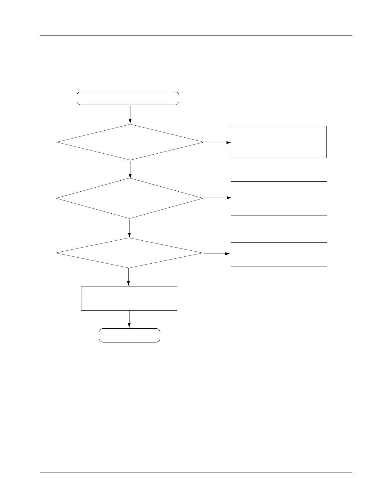
9. Flow C hart of Troubleshooting
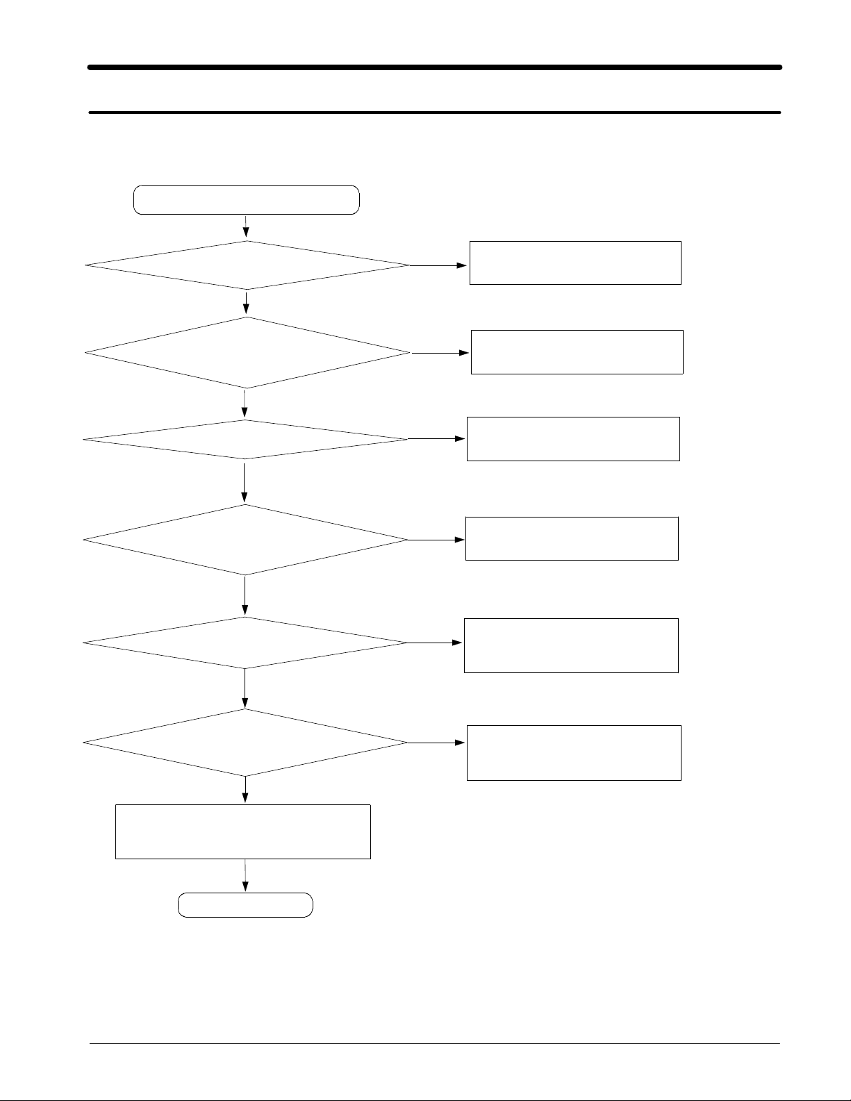
9-1.
9-1-1.
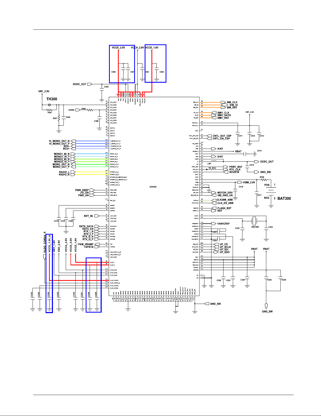
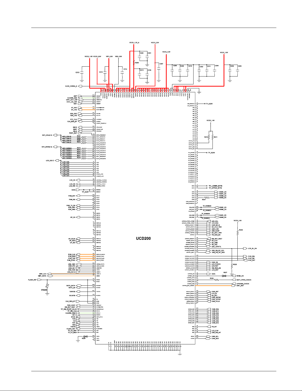
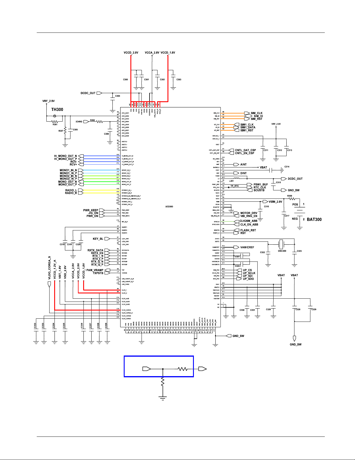
BASEBAND
Power On
Power On'does not work
'
Check the Voltage of Battery
more than
Check the current consumption
more than
Voltage of TA500=VBAT
Check the VCCD_1.8V,
VCCD_2.9V and
VCCD_1.2V_A of UCD200
Yes
No
Yes
Yes
3.3V
100
mA
Yes
No
No
?
No
Change the Battery
Download again
Check the related circuit
Check the related circuit
Yes
Check VRF_2.9V of RFT100
Yes
Check CLK26M_DBB on C117
Freq
Check the initial operation
=26
END
MHz
Yes
Yes
No
Check the UCD300 and C312, C313,
C103, C104, C105, C107
No
Check OSC100 and RFT100
9-1
SAMSUNG Proprietary-Contents may change without notice
This Document can not be used without Samsung's authorization
Page 2
Flow Chart of Troubleshooting
9-2
SAMSUNG Proprietary-Contents may change without notice
This Document can not be used without Samsung's authorization
Page 3
Flow Chart of Troubleshooting
9-3
SAMSUNG Proprietary-Contents may change without notice
This Document can not be used without Samsung's authorization
Page 4
Flow Chart of Troubleshooting
9-4
SAMSUNG Proprietary-Contents may change without notice
This Document can not be used without Samsung's authorization
Page 5
Flow Chart of Troubleshooting
9-5
SAMSUNG Proprietary-Contents may change without notice
This Document can not be used without Samsung's authorization
Page 6
Flow Chart of Troubleshooting
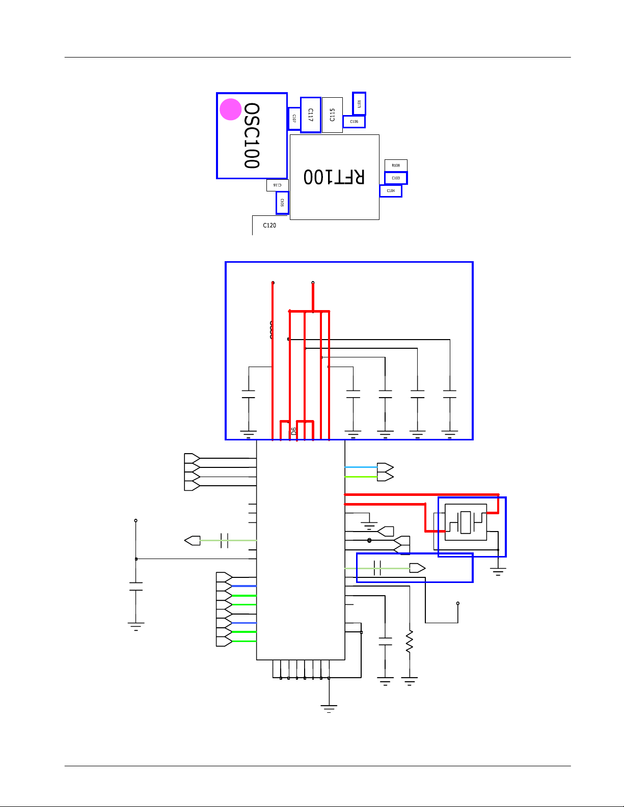
VRF_2.9V
C116
RTX_I_P
RTX_I_N
RTX_Q_P
RTX_Q_N
C115
GSM850_LNA_IN_P
GSM900_LNA_IN_P
DCS_LNA_IN_P
PCS_LNA_IN_P
GSM850_LNA_IN_N
GSM900_LNA_IN_N
DCS_LNA_IN_N
PCS_LNA_IN_N
VCCD_2.9V
L101
C106
A1
B2
B1
C2
E5
F5
G5
E2
E3
E4
A7
B7
E7
F7
A6
C7
D7
G7
1
C
IG
D
A
D
D
AX
V
B
BX
FE1
FE2
FE3
FSYS2
FSYS3
FSYSEN
RX1
RX2
RX3
RX4
RX1X
RX2X
RX3X
RX4X
D
N
G
6
B
4
6
3
F
D
G
2
L
L
S
P
M
D
D
D
D
V
V
RFT100
D
D
N
N
G
G
4
4
1
C
D
D
VRF_2.9V
5
1
5
3
F
C
A
B
X
X
R
D
D
V
D
N
G
O
G
T
C
E
D
V
R
D
D
X
V
D
R
V
T
D
D
V
XOMODE
CTRLCLK
CTRLDA
CTRLEN
SYSCLK
SYSCLKEN
REFR
REGC
VBIAS
D
D
D
N
N
N
G
G
G
5
6
2
6
F
F
E
D
O
X
D
D
V
TX1
TX2
XT
XO
NC
NC
D
N
G
A3
A2
G1
G2
F4
D2
D3
C3
E1
G3
A4
C6
G6
1
2
C107
C117
TP_SBDT
C120
C103
GSM_PAM_IN
DPCS_PAM_IN
SBCK
SBDT26MHZ_BT
SBLE
R108
C104
OSC100
2
CLK26M_DBB
VRF_2.9V
C105
1
43
9-6
SAMSUNG Proprietary-Contents may change without notice
This Document can not be used without Samsung's authorization
Page 7
Flow Chart of Troubleshooting
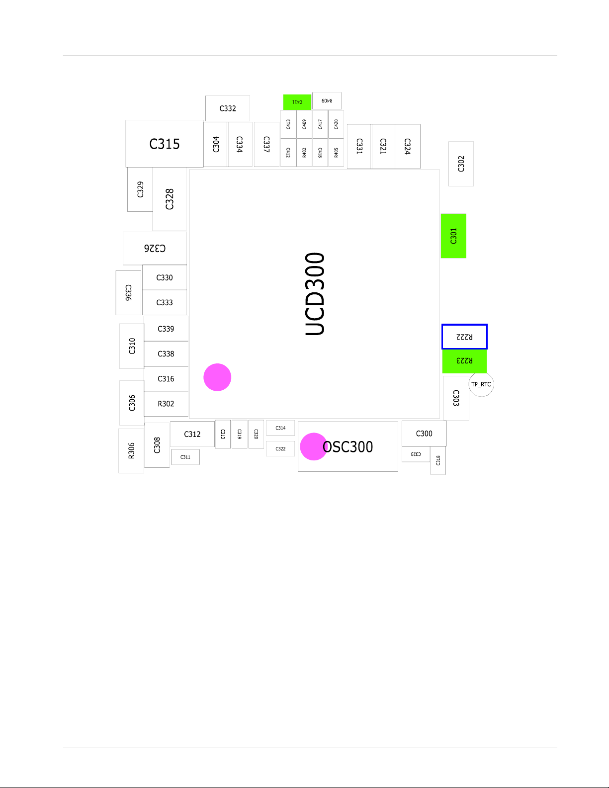
9-1-2.
Initial
Initial Failure
Yes
RST
check the R222)
(
="H
END
igh
Yes
"?
No
Check the circuit related to reset
9-7
SAMSUNG Proprietary-Contents may change without notice
This Document can not be used without Samsung's authorization
Page 8
Flow Chart of Troubleshooting
9-8
SAMSUNG Proprietary-Contents may change without notice
This Document can not be used without Samsung's authorization
Page 9
Flow Chart of Troubleshooting
R222
R223
NTSRTTSR
9-9
SAMSUNG Proprietary-Contents may change without notice
This Document can not be used without Samsung's authorization
Page 10
Flow Chart of Troubleshooting
9-10
SAMSUNG Proprietary-Contents may change without notice
This Document can not be used without Samsung's authorization
Page 11
Flow Chart of Troubleshooting
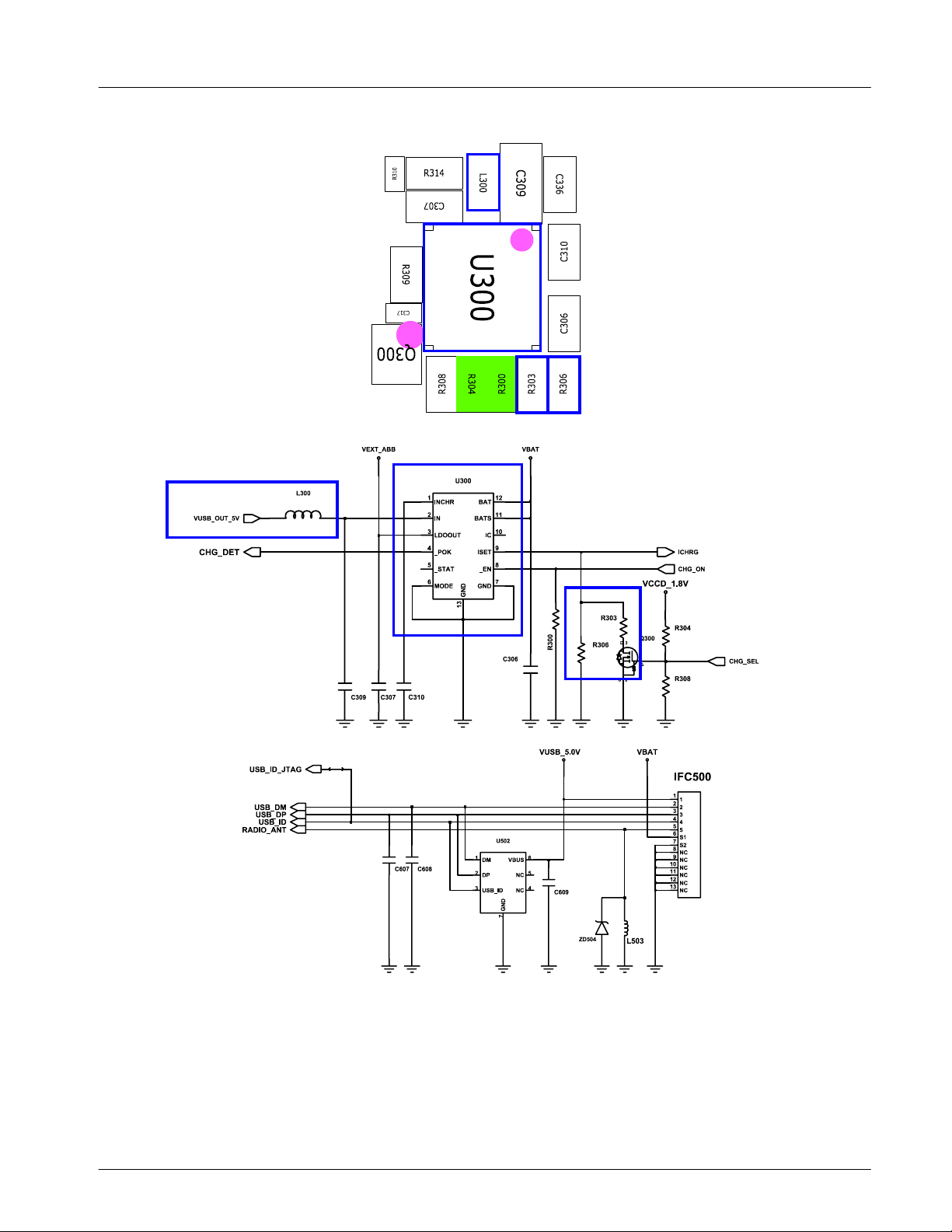
9-1-3.
Charging Part
Abnormal charging part
Check the Voltage Of L300.
Check the U300 pin
under
under
5.0V?
0.4
Yes
Yes
V?
Yes
No
4.
No
Check the circuit related to
VUSB_OUT_5V
Check the circuit related
Check the R306
R303
&
=4.3
Replace U300
END
=16
Kohm?
Yes
Kohm?
No
Replace R306, R303
9-11
SAMSUNG Proprietary-Contents may change without notice
This Document can not be used without Samsung's authorization
Page 12
Flow Chart of Troubleshooting
9-12
SAMSUNG Proprietary-Contents may change without notice
This Document can not be used without Samsung's authorization
Page 13
Flow Chart of Troubleshooting
9-13
SAMSUNG Proprietary-Contents may change without notice
This Document can not be used without Samsung's authorization
Page 14

Flow Chart of Troubleshooting
9-1-4.
Sim Part
Phone can't access SIM Card
Check the VSIM_2.9V of SIM500
Check the circuit around SIM500
Yes
2.9V ?
C504, C507)
(
Yes
input circuitry
Yes
END
No
Check the circuit related
No
Check the related circuit of SIM500
9-14
SAMSUNG Proprietary-Contents may change without notice
This Document can not be used without Samsung's authorization
Page 15

Flow Chart of Troubleshooting
9-15
SAMSUNG Proprietary-Contents may change without notice
This Document can not be used without Samsung's authorization
Page 16

Flow Chart of Troubleshooting
9-1-5.
Microphone Part
Microphone does not work
Yes
Check the connection
from MIC
Yes
Check the circuit
from UCD3
VAMICREF
00 to
Yes
On booting,
≒
2.5V ?
MIC
No
No
No
Resolder MIC
Check the path from Main IC to MIC
Check UCD300
Yes
Check the MIC
Yes
END
No
Replace the MIC
9-16
SAMSUNG Proprietary-Contents may change without notice
This Document can not be used without Samsung's authorization
Page 17

Flow Chart of Troubleshooting
9-17
SAMSUNG Proprietary-Contents may change without notice
This Document can not be used without Samsung's authorization
Page 18

Flow Chart of Troubleshooting
9-18
SAMSUNG Proprietary-Contents may change without notice
This Document can not be used without Samsung's authorization
Page 19

Flow Chart of Troubleshooting
9-1-6.
Receiver Part
There is no sound from the Receiver
Is the terminal of Receiver
Is there any signals at the
C400 and C401 of UCD3
O.K
END
Yes
?
Yes
Yes
00?
No
Replace the Receiver
No
CheckUCD300,C400, C401
9-19
SAMSUNG Proprietary-Contents may change without notice
This Document can not be used without Samsung's authorization
Page 20

Flow Chart of Troubleshooting
9-20
SAMSUNG Proprietary-Contents may change without notice
This Document can not be used without Samsung's authorization
Page 21

Flow Chart of Troubleshooting
9-1-7.
Speaker Part
Speaker does not work
Is the terminal of speake
SPK+&SPK
OK?
Check the
HIGH"
"
Yes
Yes
r
-
No
check the speaker
No
Resolder SPK+(L401)
SPK-(L402)
Check HI_MONO_OUT_P,N check the element related
Yes
Change speaker
Is it works?
Yes
END
No
No
Resolder of replace U400
9-21
SAMSUNG Proprietary-Contents may change without notice
This Document can not be used without Samsung's authorization
Page 22

Flow Chart of Troubleshooting
9-22
SAMSUNG Proprietary-Contents may change without notice
This Document can not be used without Samsung's authorization
Page 23

Flow Chart of Troubleshooting
9-1-8.
Camera part
Camera" function does not work
"
Is the Camera connected
Is the Camera working?
CAM_2.8V_A
Check C113, C100)
(
CAM_2.8V
with SUB PBA
Yes
Yes
=2.8
Check C101)
(
CAM_1.8V
Check C102)
(
Yes
=2.8
=1.8?
V?
V?
No
No
No
Reconnect the camera module
Change the camera module
Change SUB PBA
Yes
Reconnect Main Connector
HEA600
Yes
END
9-23
SAMSUNG Proprietary-Contents may change without notice
This Document can not be used without Samsung's authorization
Page 24

Flow Chart of Troubleshooting
9-24
SAMSUNG Proprietary-Contents may change without notice
This Document can not be used without Samsung's authorization
Page 25

Flow Chart of Troubleshooting
9-25
SAMSUNG Proprietary-Contents may change without notice
This Document can not be used without Samsung's authorization
Page 26

Flow Chart of Troubleshooting
9-1-9.
Radio part
Radio does not work
check VCCD_1.8V on
check VCCD_2.9V on
Resolder the U401
Yes
R502, R503
L405, C425
Is it
Is it
1.8
2.9
V?
Yes
V?
Yes
Resolder or Replace R502, R503
No
Resolder L405, C425
END
9-26
SAMSUNG Proprietary-Contents may change without notice
This Document can not be used without Samsung's authorization
Page 27

Flow Chart of Troubleshooting
9-27
SAMSUNG Proprietary-Contents may change without notice
This Document can not be used without Samsung's authorization
Page 28

Flow Chart of Troubleshooting
9-2.
9-2-1.
RF
EGSM RX
NORMAL CONDITION
catch the channel?
YES
FEM100CHECK
pin
11≥-65
FEM100CHECK
pin
3, 4≥-65
RFT100 CHECK
C114, C119
dBm
dBm
YES
-65
≥
YES
YES
dBm
NO
L150, L100, C101, L102, C100, R100, L106
NO
?
NO
?
NO
?
FEM1
resolder or change
resolder or change
resolder or change
00,
FEM1
RFT100
RFS
CHECK soldered
100
00
CONTINUOUS RX ON
RF INPUT
AMP
:-50
:62
dBm
CH
RFT100
VCCD_2.9V, VRF_2.9V
2.9V ?
YES
OSC100 CHECK
pin
1, 3
freq
MHz
:26
: 380
O.K?
END
mV?
YES
YES
?
Vp-p
GSM Receiver is
NO
:
NO
NO
CHECK soldered C106, C101, C107, C103, C104, C105
OSC
change or resolder
100
GSM RX path component
resolder or change
or
Change MAIN PBA
9-28
SAMSUNG Proprietary-Contents may change without notice
This Document can not be used without Samsung's authorization
Page 29

Flow Chart of Troubleshooting
9-2-2.
DCS RX
NORMAL CONDITION
catch the channel?
YES
FEM100CHECK
pin
11≥-65
FEM100CHECK
pin
5, 6≥-65
RFT100 CHECK
L112, L115
VCCD_2.9V, VRF_2.9V
≥
RFT100
2.9V ?
dBm
dBm
YES
-65
YES
YES
dBm
NO
L150, L100, C101, L102, C100, R100, L106
NO
?
NO
?
NO
?
NO
:
FEM1
resolder or change
resolder or change
resolder or change
CHECK soldered C106, C101, C107, C103, C104, C105
00,
FEM1
RFT100
RFS
CHECK soldered
100
00
Change MAIN PBA
CONTINUOUS RX ON
RF INPUT
AMP
or
:-50
: 698
dBm
CH
YES
OSC100 CHECK
pin
1, 3
freq
MHz
:26
: 380
O.K?
END
mV?
YES
YES
?
Vp-p
GSM Receiver is
NO
change or resolder
NO
OSC
100
DCS RX path component
resolder or change
9-29
SAMSUNG Proprietary-Contents may change without notice
This Document can not be used without Samsung's authorization
Page 30

Flow Chart of Troubleshooting
9-2-3. P
CS RX
NORMAL CONDITION
catch the channel?
YES
FEM100CHECK
pin
11≥-65
FEM100CHECK
pin
7, 8≥-65
RFT100 CHECK
L116, L119
dBm
dBm
YES
-65
≥
YES
YES
dBm
NO
L150, L100, C101, L102, C100, R100, L106
NO
?
NO
?
NO
?
FEM1
resolder or change
resolder or change
resolder or change
00,
FEM1
RFT100
RFS
CHECK soldered
100
00
CONTINUOUS RX ON
RF INPUT
AMP
:-50
: 661
dBm
CH
RFT100
VCCD_2.9V, VRF_2.9V
2.9V ?
YES
OSC100 CHECK
pin
1, 3
freq
MHz
:26
: 380
O.K?
END
mV?
YES
YES
?
Vp-p
GSM Receiver is
NO
:
NO
NO
CHECK soldered C106, C101, C107, C103, C104, C105
OSC
change or resolder
100
PCS RX path component
resolder or change
or
Change MAIN PBA
9-30
SAMSUNG Proprietary-Contents may change without notice
This Document can not be used without Samsung's authorization
Page 31

Flow Chart of Troubleshooting
9-2-4.
EGSM TX
FEM100 pin
11
about
dBm?
2~3
YES
RFS
L150,L100,C101,
100,
L102,C100,R100,L106
check&change
NO
:
PAM
pin
17,18 : 3.3~4.
V?
2
PAM
pin
3 : 1.2V ?
FEM100pin
about
:-5
PAM
pin
2:2.8
100
100
100
YES
YES
dBm
YES
NO
11
?
V?
NO
NO
NO
PAM
pin
2:2.8
check&change
100
V?
YES
BATTERY
Check R107
NO
CD300
U
check&change
CONTINOUS TX ON CONDITION
TX POWER DAC:
REF LEV.
RBW
VBW
SPAN
ATT.
CH
600
:62
: 100
:100
:10
:20
CODE APPLIED
KHz
KHz
MHz
dBm
:10
dB
CD300
U
C106,L101,C107
C103,C104,C105
,
change orresolder
YES
PAM
100
change or resolder
NO
CP200
U
check
RFT100
VCCD_2.9V, VRF_2.9V
:2.9V?
YES
pin
Vp-p
change or resolder
OSC100
1,3 : 26
:380
RFT100
Is it work?
END
MHz
YES
YES
mV?
NO
?
OSC
change or resolder
NO
UCD300
change or resolder
100
9-31
SAMSUNG Proprietary-Contents may change without notice
This Document can not be used without Samsung's authorization
Page 32

Flow Chart of Troubleshooting
9-2-5.
DCS TX
FEM100 pin
about
RFS
L150,L100,C101,
100,
L102,C100,R100,L106
check&change
NO
2~3
YES
11
dBm?
pin
:
PAM
100
17,18 : 3.3~4.
V?
2
PAM
pin
3 : 1.2V ?
FEM100pin
about
:-5
PAM
pin
2:2.8
100
100
YES
YES
dBm
YES
NO
11
?
V?
NO
NO
NO
PAM
100
pin
2:2.8
YES
BATTERY
check&change
Check R107
V?
NO
CD300
U
check&change
CONTINOUS TX ON CONDITION
TX POWER DAC:
CH
RBW
VBW
SPAN
REF LEV.
ATT.
CODE APPLIED
520
:
698
KHz
: 100
KHz
:100
MHz
:10
dBm
:10
dB
:20
CD300
U
C106,L101,C107
C103,C104,C105
,
change orresolder
YES
PAM
100
change or resolder
NO
CP200
U
check
RFT100
VCCD_2.9V, VRF_2.9V
:2.9V?
YES
pin
Vp-p
change or resolder
OSC100
1,3 : 26
:380
RFT100
Is it work?
END
MHz
YES
YES
mV?
?
NO
OSC
change or resolder
NO
UCD300
change or resolder
100
9-32
SAMSUNG Proprietary-Contents may change without notice
This Document can not be used without Samsung's authorization
Page 33

Flow Chart of Troubleshooting
9-2-6. P
CS TX
FEM100 pin
about
RFS
L150,L100,C101,
100,
L102,C100,R100,L106
check&change
NO
2~3
YES
11
dBm?
pin
:
PAM
100
17,18 : 3.3~4.
V?
2
PAM
pin
3 : 1.2V ?
FEM100pin
about
:-5
PAM
pin
2:2.8
100
100
YES
YES
dBm
YES
NO
11
?
V?
NO
NO
NO
PAM
100
pin
2:2.8
YES
BATTERY
check&change
Check R107
V?
NO
CD300
U
check&change
CONTINOUS TX ON CONDITION
TX POWER DAC:
REF LEV.
RBW
VBW
SPAN
ATT.
520
CH
:
: 100
:100
:10
:20
CODE APPLIED
661
KHz
KHz
MHz
dBm
:10
dB
CD300
U
C106,L101,C107
C103,C104,C105
,
change orresolder
YES
PAM
100
change or resolder
NO
CP200
U
check
RFT100
VCCD_2.9V, VRF_2.9V
:2.9V?
YES
pin
Vp-p
change or resolder
OSC100
1,3 : 26
:380
RFT100
Is it work?
END
MHz
YES
YES
mV?
?
NO
OSC
change or resolder
NO
UCD300
change or resolder
100
9-33
SAMSUNG Proprietary-Contents may change without notice
This Document can not be used without Samsung's authorization
Page 34

Flow Chart of Troubleshooting
9-34
SAMSUNG Proprietary-Contents may change without notice
This Document can not be used without Samsung's authorization
Page 35

Flow Chart of Troubleshooting
VRF_2.9V
C116
RTX_I_P
RTX_I_N
RTX_Q_P
RTX_Q_N
GSM850_LNA_IN_P
GSM900_LNA_IN_P
DCS_LNA_IN_P
PCS_LNA_IN_P
GSM850_LNA_IN_N
GSM900_LNA_IN_N
DCS_LNA_IN_N
PCS_LNA_IN_N
C115
VCCD_2.9V
C106
A1
B2
B1
C2
E5
F5
G5
E2
E3
E4
A7
B7
E7
F7
A6
C7
D7
G7
L101
A
AX
B
BX
FE1
FE2
FE3
FSYS2
FSYS3
FSYSEN
RX1
RX2
RX3
RX4
RX1X
RX2X
RX3X
RX4X
1
C
6
B
4
G
G
I
D
D
D
V
D
N
G
4
C
6
3
F
D
2
L
L
S
P
M
D
D
D
D
V
V
RFT100
D
D
N
N
G
G
4
1
D
D
VRF_2.9V
5
5
3
C
A
B
X
X
G
O
T
R
E
C
D
D
R
V
D
X
D
D
V
V
R
D
T
V
D
D
V
XOMODE
CTRLCLK
CTRLDA
CTRLEN
SYSCLK
SYSCLKEN
REFR
REGC
VBIAS
D
D
D
D
N
N
N
N
G
G
G
G
5
6
2
F
E
D
C107
C103
1
F
O
X
D
D
A3
V
TX1
A2
TX2
G1
XT
G2
XO
F4
D2
D3
C3
TP_SBDT
C117
E1
G3
A4
C6
G6
1
NC
2
NC
D
N
G
6
F
C120
GSM_PAM_IN
DPCS_PAM_IN
SBCK
SBDT26MHZ_BT
SBLE
R108
C104
2
CLK26M_DBB
VRF_2.9V
C105
OSC100
1
43
9-35
SAMSUNG Proprietary-Contents may change without notice
This Document can not be used without Samsung's authorization
Page 36

Flow Chart of Troubleshooting
9-2-7.
Bluetooth part
Bluetooth connection disable
Check BT function ON
Check power of U100,
VBT_1.8V
VBT_1.5V
Check pin A3 of
(26
≒
≒
MHz)
Yes
1.8
1.5
Yes
Yes
V,
V?
U100
No
Enable BT function
No
Resolder U100
No
Resolder C115
Yes
Check the assembled
status of F100, L120, L121,
C136, C130, C131, C134
Yes
Check the assembled status
of ANT101
Yes
END
No
No
Resolder error parts
Resolder ANT101
9-36
SAMSUNG Proprietary-Contents may change without notice
This Document can not be used without Samsung's authorization
Page 37

Flow Chart of Troubleshooting
9-37
SAMSUNG Proprietary-Contents may change without notice
This Document can not be used without Samsung's authorization
Page 38

Flow Chart of Troubleshooting
VRF_2.9V
C116
RTX_I_P
RTX_I_N
RTX_Q_P
RTX_Q_N
GSM850_LNA_IN_P
GSM900_LNA_IN_P
DCS_LNA_IN_P
PCS_LNA_IN_P
GSM850_LNA_IN_N
GSM900_LNA_IN_N
DCS_LNA_IN_N
PCS_LNA_IN_N
C115
VCCD_2.9V
C106
A1
B2
B1
C2
E5
F5
G5
E2
E3
E4
A7
B7
E7
F7
A6
C7
D7
G7
L101
A
AX
B
BX
FE1
FE2
FE3
FSYS2
FSYS3
FSYSEN
RX1
RX2
RX3
RX4
RX1X
RX2X
RX3X
RX4X
1
C
G
I
D
D
D
V
D
N
G
6
B
4
3
F
G
2
L
S
L
P
M
D
D
D
D
V
V
RFT100
D
D
N
N
G
G
4
1
C
D
VRF_2.9V
6
5
3
C
D
B
X
X
G
T
R
E
D
D
R
D
X
D
V
V
R
T
D
D
V
XOMODE
CTRLCLK
CTRLDA
CTRLEN
SYSCLK
SYSCLKEN
D
D
D
N
N
N
G
G
G
5
4
6
E
D
D
5
A
O
C
V
D
D
V
REFR
REGC
VBIAS
D
N
G
2
F
C107
1
F
O
X
D
D
A3
V
TX1
A2
TX2
G1
XT
G2
XO
F4
D2
D3
C3
E1
G3
A4
C6
G6
1
NC
2
NC
D
N
G
6
F
TP_SBDT
C117
C120
C103
GSM_PAM_IN
DPCS_PAM_IN
SBCK
R108
SBDT26MHZ_BT
SBLE
C104
CLK26M_DBB
VRF_2.9V
C105
OSC100
2
1
43
9-38
SAMSUNG Proprietary-Contents may change without notice
This Document can not be used without Samsung's authorization
Page 39

Block Diagrams
7.
7-1.
Block Diagram
7-1
SAMSUNG Proprietary-Contents may change without notice
This Document can not be used without Samsung's authorization
Page 40

Block Diagrams
7-2.
RF Blcok Diagram
7-2
SAMSUNG Proprietary-Contents may change without notice
This Document can not be used without Samsung's authorization
Page 41

Block Diagrams
7-3.
Audio Block Diagram
7-3
SAMSUNG Proprietary-Contents may change without notice
This Document can not be used without Samsung's authorization
Page 42

PCB Diagrams
8.
Main top view]
[
8-1
SAMSUNG Proprietary-Contents may change without notice
This Document can not be used without Samsung's authorization
Page 43

PCB Diagrams
Main Bottom view]
[
8-2
SAMSUNG Proprietary-Contents may change without notice
This Document can not be used without Samsung's authorization
 Loading...