

Page 1
GSM TELEPHONE
GT-S3600L
GSM TELEPHONE
CONTENTS
Safety Precautions
1.
Specification
2.
Product Function
3.
Array course control
4.
Exploded View and Parts list
5.
MAIN Electrical Parts List
6.
Block Diagrams
7.
PCB Diagrams
8.
Chart of Troubleshooting
9.
Reference data
10.
Disassembly and Assembly
11.
Instructions
Page 2
GSPN(Global Service Partner Network)
Country Web Site
North America service.samsungportal.com
Latin America latin.samsungportal.com
CIS cis.samsungportal.com
Europe europe.samsungportal.com
China china.samsungportal.com
Asia asia.samsungportal.com
Mideast
This Service Manual isaproperty of Samsung Electronics Co.,Ltd.
Any unauthorized use of Manual can be punished under applicable
International and/or domestic law.
Africa mea.samsungportal.com
&
Samsung Electronics Co.,Ltd.
ⓒ
2009. 01.
Rev.1.0
Page 3
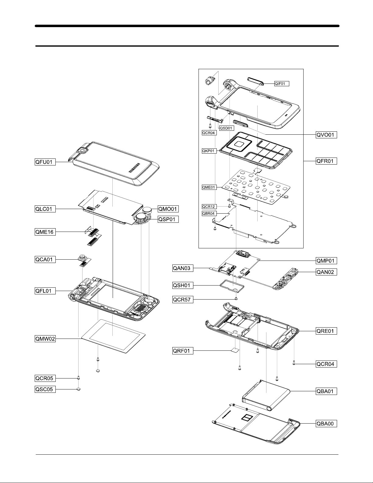
Exploded View and Parts List
5.
5-1.
Cellular phone Exploded View
5-1
SAMSUNG Proprietary-Contents may change without notice
This Document can not be used without Samsung's authorization
Page 4
- This Document can not be used without Samsung's authorization -
5-2. Cellular phone Parts list : GT-S3600RKAXEB
Design LOC
QAN01
QAN03
QBA00
QBA01
QBR04
QCA01
QCR04
QCR04
QCR05
QCR12
QCR57
QFL01
QFU01
QIF01
QKP01
QME01
QME16
QMO01
QMW02
QRE01
QRF01
QSC05
QSD01
QSH01
QSP01
QVO01
INNER BATTERY PACK-880MAH,BLK,UNI,MAIN
ASSY CAMERA-GT_S3600(1.3M)
ASSY KEYPAD-MAIN(OPEN/BLK)
KEY FPCB-MAIN KEY PBA(GT-S3600)
UNIT-CON TO CON(GT_S3600)
RMO RUBBER-SCREW FOLDER
Description
INTENNA-GT_S3600
INTENNA-BT(GT_S3600)
PMO COVER-BATTERY
ASSY BRACKET-KEYPAD
SCREW-MACHINE
SCREW-MACHINE
SCREW-MACHINE
SCREW-MACHINE
SCREW-MACHINE
ASSY CASE-FOLDER LOWER
ASSY CASE-FOLDER UPPER
PMO COVER-IF
MOTOR DC-SPHV8400
PCT WINDOW-MAIN
ASSY CASE-REAR
TAPE-RF SHEET
PMO COVER-SD
ICT SHIELD-TOP
SPEAKER
PMO KEY-VOLUME
SEC CODE
GH42-01768A
GH42-01770A
GH72-49614B
GH43-03248A
GH98-10170A
GH96-03404A
6001-001479
6001-001479
6001-001478
6001-001530
6001-002001
GH98-10165A
GH98-10164B
GH72-49615A
GH98-10168A
GH59-06323A
GH59-06297A
GH31-00187A
GH72-50148A
GH98-10167B
GH74-41040B
GH73-12196A
GH72-49616A
GH70-04188A
3001-002430
GH72-49624A
Page 5
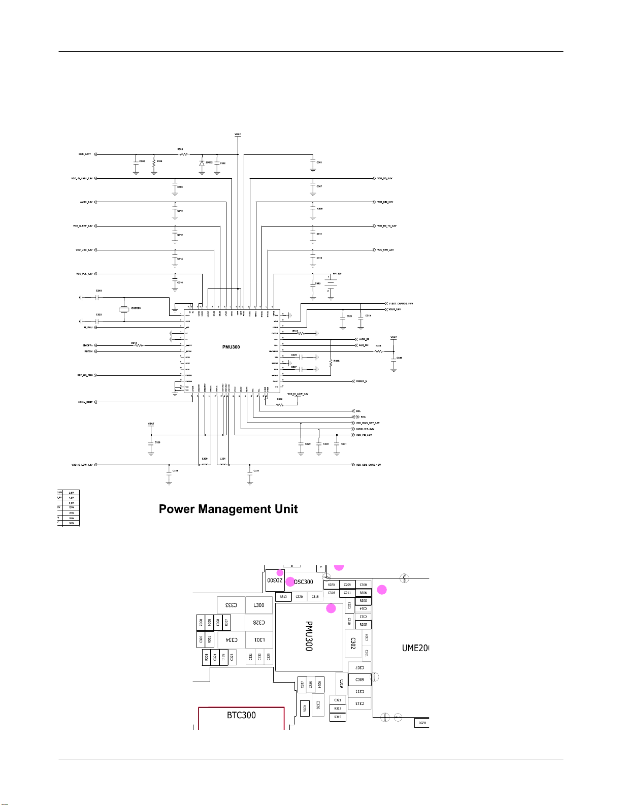
MAIN Electrical Parts List
6.
Design LOC SEC CODE Discription
ZD302
D100
ZD300,ZD303,ZD400
ZD406
ZD401,ZD402
U201
U402
UME200
PAM100
U400
U300
PMU300
U103
U100
UCP200
U102
VR300
R103,R105,R209,R303
R313
R107
R102,R106,R200,R201
R202,R208,R406,R422
R207
R312
R300
R304
R205,R301,R302,R308
R315
R311,R407
R314
R430,R431
R420,R423
R203,R204,R212,R434
R435
R403,R404,R413,R414
R307,R316,R421
R405,R408,R409,R410
R411
R210,R211
R317,R400,R401,R432
R402
R206,R412
0403-001547
0404-001317
0406-001306
0406-001306
0406-001319
0801-003022
0801-003024
1108-000187
1201-002742
1201-002764
1203-004883
1203-005467
1204-002906
1205-003283
1205-003336
1205-003604
1404-001221
2007-000140
2007-000141
2007-000143
2007-000148
2007-000148
2007-000149
2007-000151
2007-000157
2007-000159
2007-000162
2007-000162
2007-000165
2007-000166
2007-000170
2007-000171
2007-000172
2007-000172
2007-000242
2007-000758
2007-001291
2007-001291
2007-001319
2007-001333
2007-001339
2007-002796
DIODE-ZENER
DIODE-SCHOTTKY
DIODE-TVS
DIODE-TVS
DIODE-TVS
IC
IC
MEMORY
IC
IC
IC
IC
IC
IC
IC
IC
THERMISTOR
R-CHIP
R-CHIP
R-CHIP
R-CHIP
R-CHIP
R-CHIP
R-CHIP
R-CHIP
R-CHIP
R-CHIP
R-CHIP
R-CHIP
R-CHIP
R-CHIP
R-CHIP
R-CHIP
R-CHIP
R-CHIP
R-CHIP
R-CHIP
R-CHIP
R-CHIP
R-CHIP
R-CHIP
R-CHIP
6-1
SAMSUNG Proprietary-Contents may change without notice
This Document can not be used without Samsung's authorization
Page 6
Main Electrical Parts List
Design LOC SEC CODE Discription
R424,R425
R305
R309
R416
R306,R310
R433
C107,C114,C131,C315
C121,C122,C135,C137
C417,C419,C427
C110,C130
C323
C318
C320
C204,C205,C212
C111,C123,C423,C424
C335,C400,C403,C405
C134
C407,C408
C432,C433,C434,C435
C436,C437,C438,C439
C143
C115,C119
C213
C402,C411
C128,C129
C108,C112,C116,C118
C144
C124,C127
C203,C211
C100,C101,C102,C103
C104,C105,C106,C120
C132,C133,C140,C200
C201,C202,C206,C207
C208,C209,C210,C214
C215,C322,C324,C327
C332,C401,C404,C409
C412,C414,C415,C416
C307,C311,C313
C136,C138,C301,C308
C310,C312,C314,C316
C325,C329,C330,C331
C139,C141,C300,C418
2007-003006
2007-007573
2007-007589
2007-007875
2007-008354
2007-008531
2203-000233
2203-000254
2203-000254
2203-000278
2203-000311
2203-000425
2203-000550
2203-000679
2203-000812
2203-000854
2203-000995
2203-001153
2203-001259
2203-001259
2203-002668
2203-005050
2203-005055
2203-005057
2203-005234
2203-005281
2203-005288
2203-005446
2203-005450
2203-006048
2203-006048
2203-006048
2203-006048
2203-006048
2203-006048
2203-006048
2203-006048
2203-006208
2203-006257
2203-006257
2203-006257
2203-006260
C-CERAMIC,CHIP
C-CERAMIC,CHIP
C-CERAMIC,CHIP
C-CERAMIC,CHIP
C-CERAMIC,CHIP
C-CERAMIC,CHIP
C-CERAMIC,CHIP
C-CERAMIC,CHIP
C-CERAMIC,CHIP
C-CERAMIC,CHIP
C-CERAMIC,CHIP
C-CERAMIC,CHIP
C-CERAMIC,CHIP
C-CERAMIC,CHIP
C-CERAMIC,CHIP
C-CERAMIC,CHIP
C-CERAMIC,CHIP
C-CERAMIC,CHIP
C-CERAMIC,CHIP
C-CERAMIC,CHIP
C-CERAMIC,CHIP
C-CERAMIC,CHIP
C-CERAMIC,CHIP
C-CERAMIC,CHIP
C-CERAMIC,CHIP
C-CERAMIC,CHIP
C-CERAMIC,CHIP
C-CERAMIC,CHIP
C-CERAMIC,CHIP
C-CERAMIC,CHIP
C-CERAMIC,CHIP
C-CERAMIC,CHIP
C-CERAMIC,CHIP
C-CERAMIC,CHIP
C-CERAMIC,CHIP
C-CERAMIC,CHIP
R-CHIP
R-CHIP
R-CHIP
R-CHIP
R-CHIP
R-CHIP
6-2
SAMSUNG Proprietary-Contents may change without notice
This Document can not be used without Samsung's authorization
Page 7
Main Electrical Parts List
Design LOC SEC CODE Discription
C421
C326
C319
C302,C328
C216,C304,C305,C306
C426,C428,C429,C431
C333,C334
C303,C420,C430
C217
C309
C321
TA401
TA100,TA300,TA400
L110
L116
L101
L109
C145
C117
L104,L111
L113,L114
L106
L115
R104
L300,L301
OSC300
OSC100
F400,F401,F402,F403
F404
F100
U101
L400,L401,L402,L403
L100
L404,L405
RFS101
RFS100
SIM300
CD300
IFC400
HDC300
BTC300
HDC400
BAT300
Please consult the GSPN website (Samsung Portal) for the most recent version of the product's part list.
2203-006260
2203-006324
2203-006348
2203-006361
2203-006399
2203-006399
2203-006474
2203-006562
2203-006824
2203-006825
2203-006841
2404-001377
2404-001381
2703-001748
2703-001750
2703-002155
2703-002170
2703-002176
2703-002207
2703-002558
2703-002608
2703-003064
2703-003121
2703-002367
2703-003498
2801-004466
2801-004787
2901-001498
2901-001498
2909-001307
2911-000116
3301-001729
3301-001756
3301-001812
3705-001448
3705-001503
3709-001391
3709-001464
3710-002568
3711-005962
3711-006256
3711-006483
4302-001177
C-CERAMIC,CHIP
C-CERAMIC,CHIP
C-CERAMIC,CHIP
C-CERAMIC,CHIP
C-CERAMIC,CHIP
C-CERAMIC,CHIP
C-CERAMIC,CHIP
C-CERAMIC,CHIP
C-CERAMIC,CHIP
C-CERAMIC,CHIP
C-CERAMIC,CHIP
C-TA,CHIP
C-TA,CHIP
INDUCTOR-SMD
INDUCTOR-SMD
INDUCTOR-SMD
INDUCTOR-SMD
INDUCTOR-SMD
INDUCTOR-SMD
INDUCTOR-SMD
INDUCTOR-SMD
INDUCTOR-SMD
INDUCTOR-SMD
INDUCTOR-SMD
INDUCTOR-SMD
CRYSTAL-UNIT
CRYSTAL-UNIT
FILTER-EMI SMD
FILTER-EMI SMD
FILTER-DUPLEXER
FILTER
CORE-FERRITE BEAD
CORE-FERRITE BEAD
CORE-FERRITE BEAD
CONNECTOR-COAXIAL
CONNECTOR-COAXIAL
CONNECTOR-CARD EDGE
CONNECTOR-CARD EDGE
CONNECTOR-SOCKET
CONNECTOR-HEADER
CONNECTOR-HEADER
CONNECTOR-HEADER
BATTERY
6-3
SAMSUNG Proprietary-Contents may change without notice
This Document can not be used without Samsung's authorization
Page 8
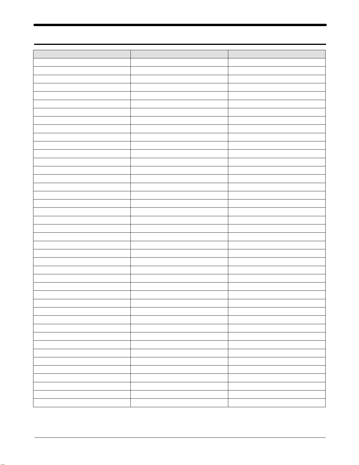
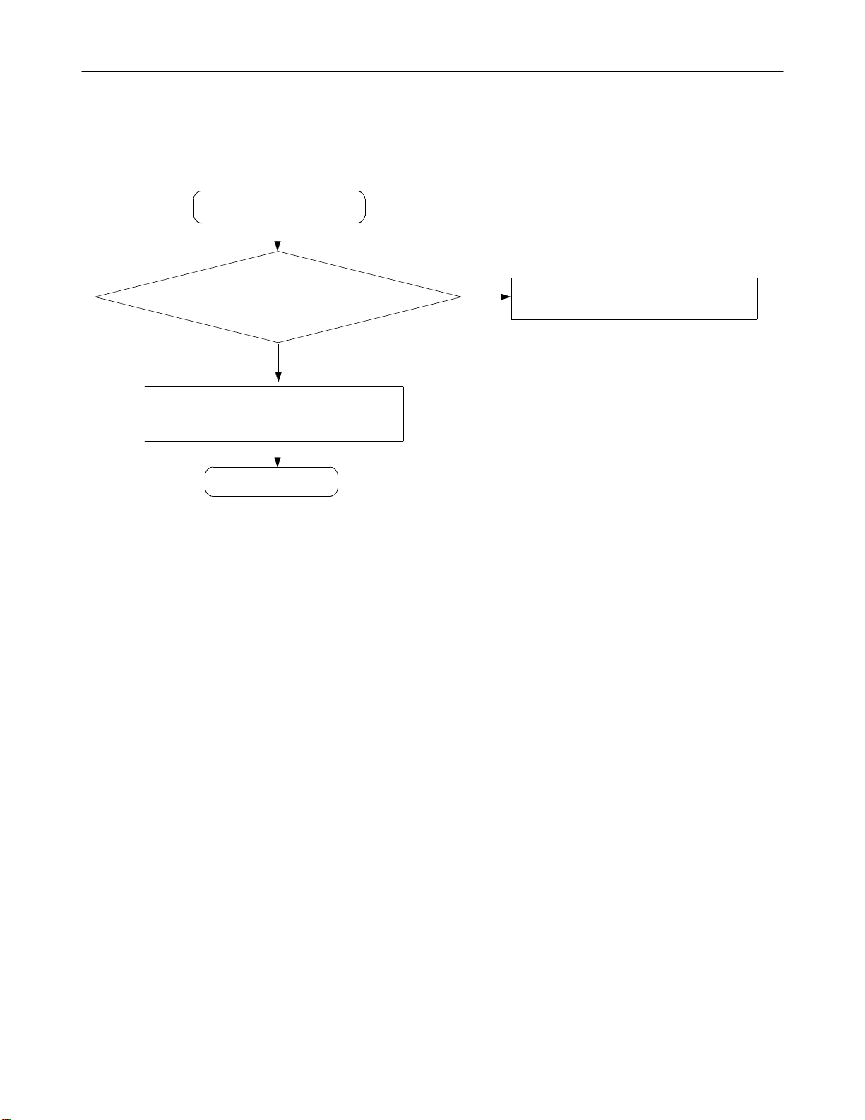
9. Поиск и устранение неполадок
9-1.
Power On
Power On'does not work
'
Yes
Check the Battery Voltage
is more than
VISA
C325(
Check the Clock at
C318
Yes
)=2.7
Yes
KHZ
=32
Yes
3.4V
V?
No
No
No
Change the Battery
Check the PMU related to VISA
Resolder OSC
300
VDD_IO_LOW)
C333(+
VDD_IO_HIGH)="H"?
C308(+
Yes
VDD_GSM_CORE)
C334(+
V?
=1.9
Yes
Check for the clock at C141
MHz
=26
Yes
Check the initial operation
Yes
&
No
No
No
Check the related circuit
Check the+VDD_GSM_CORE circuit
Check the clock generation circuit
related to
(
OSC100
)
END
9-1
SAMSUNG Proprietary-Contents may change without notice
This Document can not be used without Samsung's authorization
Page 9
Flow Chart of Troubleshooting
9-2
SAMSUNG Proprietary-Contents may change without notice
This Document can not be used without Samsung's authorization
Page 10
Flow Chart of Troubleshooting
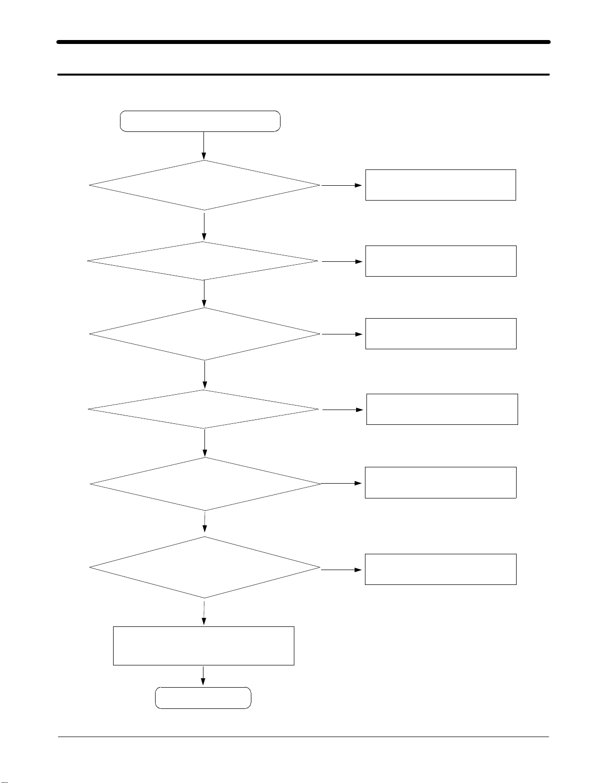
9-2.
Initial
Initial Failure
Yes
PMU300 pin7(RSTON)="H"?
Yes
Check the16bit data signal
memory CE
&
END
Yes
No
Check the circuit related to reset
9-3
SAMSUNG Proprietary-Contents may change without notice
This Document can not be used without Samsung's authorization
Page 11

Flow Chart of Troubleshooting
9-4
SAMSUNG Proprietary-Contents may change without notice
This Document can not be used without Samsung's authorization
Page 12

Flow Chart of Troubleshooting
9-3.
Charging Part
Abnormal charging part
Abnormal charging part
Check the PMU300 pin
PMU300 pin
>4.9V
34 = "
Yes
Yes
Yes
Yes
Yes
Yes
L"?
Check the circuit related to
No
1
No
No
No
Check the circuit related to
V_EXT_CHARGE
V_EXT_CHARGE
Check the circuit related to
AUX_ON signal
Check the PMU300 pin
4.2V
≒
Yes
Yes
END
46
No
No
Check the circuit related to
MES_BATT signal
9-5
SAMSUNG Proprietary-Contents may change without notice
This Document can not be used without Samsung's authorization
Page 13

Flow Chart of Troubleshooting
9-6
SAMSUNG Proprietary-Contents may change without notice
This Document can not be used without Samsung's authorization
Page 14

Flow Chart of Troubleshooting
9-4.
Sim Part
pin3 of
Phone can't access SIM Card
Yes
SIM
Check SIMCLK Signal on
pin
400
After Power ON,
SIM
1,5 = "
300ina
Yes
few second
Yes
H"?
No
Check the sim charge pump
No
Check the Clock
After SIM card insert,
SIM300pin
2="
Check the SIM Card
H(SIM_RST)"?
Yes
Yes
END
No
Replace PBA
9-7
SAMSUNG Proprietary-Contents may change without notice
This Document can not be used without Samsung's authorization
Page 15

Flow Chart of Troubleshooting
9-8
SAMSUNG Proprietary-Contents may change without notice
This Document can not be used without Samsung's authorization
Page 16

Flow Chart of Troubleshooting
9-5.
Microphone Part
Microphone does not work
Check the connection
from MIC
R315
=2.15
Yes
Yes
V?
No
Resolder MIC
No
Check the path around MIC bias circuit
Check the circuit
from
UCP20
0
Check the MIC
END
Yes
to
Yes
MIC
No
Check the path from MainIC to MIC
Replace the MIC
9-9
SAMSUNG Proprietary-Contents may change without notice
This Document can not be used without Samsung's authorization
Page 17

Flow Chart of Troubleshooting
9-10
SAMSUNG Proprietary-Contents may change without notice
This Document can not be used without Samsung's authorization
Page 18

Flow Chart of Troubleshooting
9-6.
Speaker Part(Melody)
Speaker does not work
Yes
check the signal at Pin
A4,B4 of U400>1.3V
Yes
Check the signal at
Pin
E4,E5 of U400
Yes
Is Speaker working?
No
Resolder or replace C417,C419
No
Resolder or replace U400
No
Change the Speaker
END
Yes
9-11
SAMSUNG Proprietary-Contents may change without notice
This Document can not be used without Samsung's authorization
Page 19

Flow Chart of Troubleshooting
9-12
SAMSUNG Proprietary-Contents may change without notice
This Document can not be used without Samsung's authorization
Page 20

Flow Chart of Troubleshooting
9-7.
Key Data Input
Check Initial Operation
When one of the keys is
pushed,
is it displayed on LCD?
When one of the keys is
pushed,
KBIO signal is OK?
Yes
No
Check the Dome sheet&Key Pad
Yes
No
Replace the PBA
END
Yes
9-13
SAMSUNG Proprietary-Contents may change without notice
This Document can not be used without Samsung's authorization
Page 21

Flow Chart of Troubleshooting
9-8.
Receiver Part
Receiver does not work
Is Receiver working?
Is Receiver working?
Yes
No
Resolder UCP200or change PBA
Yes
No
Replace the Receiver
Yes
END
9-14
SAMSUNG Proprietary-Contents may change without notice
This Document can not be used without Samsung's authorization
Page 22

Flow Chart of Troubleshooting
9-9.
Back Light(for Color Main LCD)
Backlight does not work
Yes
Is LCD Contrast set on high
level in the Menu?
Yes
Replace the LCD Module
END
No
Set LCD Contrast on high level
9-15
SAMSUNG Proprietary-Contents may change without notice
This Document can not be used without Samsung's authorization
Page 23

Flow Chart of Troubleshooting
9-10.
Key Back Light
Main key LED does not work
PMU300 pin23(D6VDD)C329
H?
END
Yes
Yes
=
No
Check the VDD_MAIN_KEY_3.3V line
9-16
SAMSUNG Proprietary-Contents may change without notice
This Document can not be used without Samsung's authorization
Page 24

Flow Chart of Troubleshooting
9-12.
GSM
TX ON(5Level)
Transmitter
850
CheckUCP
PAM
100
>= 1V
PAM
100
>= 20
pin1
dBm
pin
Yes
200
7
No
Resolder or Change C111
0
No
Resolder or Change PAM100
U101 pin1
dBm
>= 20
U101 pin
dBm
>= 20
RFS
100
dBm
>= 20
Ant100 Pin
dBm
>= 20
END
Yes
Yes
Yes
Pin
Yes
17
17
No
No
No
No
Resolder L110, C119,C143
Check U101
pin
10=L
pin
H(2.6V)
15=
Yes
Resolder L101, C107
Resolder L103, R104
No
Change or Resolder U101
Check ANT Switch
control circuit
Check U200
4
1
9-17
SAMSUNG Proprietary-Contents may change without notice
This Document can not be used without Samsung's authorization
Page 25

Flow Chart of Troubleshooting
9-13.
GSM
900
RX ON
RF input
Amp
U101 Pin
>= -65
U101 pin3,4
>= -68
pin
25 >= -70
pin
24 >= -70
Receiver
CH
:62
dBm
:-50
Yes
17
dBm
Yes
dBm
Yes
U10
0
dBm
dBm
No
No
Resolder L101, C107
Check U101
pin
pin1
10,
5=L
Resolder C116,C118,L111
ow
Yes
NoNo
Check ANT Switch
control circuit
Resolder U101
U100pin
>= 1V
CheckUCP
END
Yes
4,5,6,7
Yes Yes
200
No
U100pin
11,12,32,33
>=2.8V
No
Check
U101,OSC100
RF26MHz, RF PSU Part
Resolder U10
0
9-18
SAMSUNG Proprietary-Contents may change without notice
This Document can not be used without Samsung's authorization
Page 26

Flow Chart of Troubleshooting
9-14.
GSM
TX ON(5Level)
Transmitter
900
CheckUCP
PAM
100
>= 1V
PAM
100
>= 20
pin1
dBm
pin
Yes
200
7
No
Resolder or Change C111
0
No
Resolder or Change PAM100
U101 pin1
dBm
>= 20
U101 pin
dBm
>= 20
RFS
100
dBm
>= 20
Ant100 Pin
dBm
>= 20
END
Yes
Yes
Yes
Pin
Yes
17
17
No
No
No
No
Resolder L110, C119,C143
Check U101
pin
10=L
pin
H(2.6V)
15=
Yes
Resolder L101, C107
Resolder L103, R104
No
Change or Resolder U101
Check ANT Switch
control circuit
Check U200
4
1
9-19
SAMSUNG Proprietary-Contents may change without notice
This Document can not be used without Samsung's authorization
Page 27

Flow Chart of Troubleshooting
9-15.
DCS Receiver
RX ON
RF input
pin
pin
: 698
Amp
U101 Pin
U101 pin5,6
dBm
:-50
Yes
dBm
>= -65
Yes
dBm
>= -68
Yes
U10
0
23 >= -70
22 >= -70
17
CH
dBm
dBm
No
No
Resolder L101, C107
Check U101
pin
pin1
10,
5=L
Resolder C124,C127,L113
ow
Yes
NoNo
Check ANT Switch
control circuit
Resolder U101
U100pin
>= 1V
CheckUCP
END
Yes
4,5,6,7
Yes Yes
200
No
U100pin
11,12,32,33
>=2.8V
No
Check
U101,OSC100
RF26MHz, RF PSU Part
Resolder U10
0
9-20
SAMSUNG Proprietary-Contents may change without notice
This Document can not be used without Samsung's authorization
Page 28

Flow Chart of Troubleshooting
9-16.
DCS Transmitter
TX ON(0Level)
CheckUCP
PAM
PAM
>= 20
100
>= 1V
100
dBm
pin
Yes
pin1
200
1
2
No
Resolder or Change C110
No
Resolder or Change PAM100
U101 pin1
dBm
>= 20
U101 pin
dBm
>= 20
RFS
100
dBm
>= 20
Ant100 Pin
dBm
>= 20
END
Yes
Yes
Yes
Pin
Yes
17
17
No
No
No
No
Resolder L116, C144
Check U101
pin
1=L
pin
H(2.6V)
15=
Yes
Resolder L101, C107
Resolder L103, R104
No
Change or Resolder U101
Check ANT Switch
control circuit
Check U200
2
1
9-21
SAMSUNG Proprietary-Contents may change without notice
This Document can not be used without Samsung's authorization
Page 29

Flow Chart of Troubleshooting
9-17.
PCS Receiver
RX ON
RF input
pin
pin
: 661
Amp
U101 Pin
U101 pin7,8
dBm
:-50
Yes
dBm
>= -65
Yes
dBm
>= -68
Yes
U10
0
21 >= -70
20 >= -70
17
CH
dBm
dBm
No
No
Resolder L101, C107
Check U101
pin
pin1
10,
5=L
Resolder C128,C129,L114
ow
Yes
NoNo
Check ANT Switch
control circuit
Resolder U101
U100pin
>= 1V
CheckUCP
END
Yes
4,5,6,7
Yes Yes
200
No
U100pin
11,12,32,33
>=2.8V
No
Check
U101,OSC100
RF26MHz, RF PSU Part
Resolder U10
0
9-22
SAMSUNG Proprietary-Contents may change without notice
This Document can not be used without Samsung's authorization
Page 30

Flow Chart of Troubleshooting
9-18.
PCS Transmitter
TX ON(0Level)
CheckUCP
PAM
PAM
>= 20
100
>= 1V
100
dBm
pin
Yes
pin1
200
1
2
No
Resolder or Change C110
No
Resolder or Change PAM100
U101 pin1
dBm
>= 20
U101 pin
dBm
>= 20
RFS
100
dBm
>= 20
Ant100 Pin
dBm
>= 20
END
Yes
Yes
Yes
Pin
Yes
17
17
No
No
No
No
Resolder L116, C144
Check U101
pin
1=L
pin
H(2.6V)
15=
Yes
Resolder L101, C107
Resolder L103, R104
No
Change or Resolder U101
Check ANT Switch
control circuit
Check U200
2
1
9-23
SAMSUNG Proprietary-Contents may change without notice
This Document can not be used without Samsung's authorization
Page 31

Flow Chart of Troubleshooting
9-24
SAMSUNG Proprietary-Contents may change without notice
This Document can not be used without Samsung's authorization
Page 32

Flow Chart of Troubleshooting
9-25
SAMSUNG Proprietary-Contents may change without notice
This Document can not be used without Samsung's authorization
 Loading...