Samsung GT-I9100, GT-I9100p, GT-I9100g Servis Manual
GSM TELEPHONE
GT-i9100
GSM TELEPHONE
CONTENTS
Safety Precautions
1.
Specification
2.
Product Function
3.
Exploded View and Parts list
4.
MAIN Electrical Parts List
5.
Level1Repair
6.
Level2Repair
7.
Level3Repair
8.
Reference data
9.
Notice
All functionality, features, specifications and other
product information provided in this document inclu
ding, but not limited to, the benefits, design, pricing,
components, performance, availability, and capabiliti
es of the product are subject to change without
-
notice or obligation. Samsung reserves the right to
make changes to this document and the product
described herein, at anytime, without obligation on
Samsung to provide notification of such change.
:
This Service Manual isaproperty of Samsung Electronics Co.,Ltd.
Any unauthorized use of Manual can be punished under applicable
International and/or domestic law.
Samsung Electronics Co.,Ltd.
ⓒ
2011. 04.
Rev.1.0

Specification
2.
GSM General Specification
2-1.
Freq.
Band[MHz]
Uplink/
Downlink
ARFCN
range
Tx/Rx
spacing
Mod. Bit
rate/
Bit Period
Time Slot
Period/
Frame
Period
GSM850 EGSM 900 DCS1800 PCS1900
824~849
869~894
128~251
45MHz 45MHz 95MHz 80MHz 190MHz 80MHz 45MHz 45MHz
270.833kbp
s
3.692us
576.9us
4.615ms
880~915
925~960
0~124 &
975~1023
270.833kbp
s
3.692us
576.9us
4.615ms
1710~1785
1805~1880
512~885 512~810
270.833kbp
s
3.692us
576.9us
4.615ms
1850~1910
1930~1990
270.833kbp
s
3.692us
576.9us
4.615ms
WCDMA
2100
1922~1977
2112~2167
UL:
9612~9888
DL:
10562~1083
8
3.84Mcps 3.84Mcps 3.84Mcps 3.84Mcps
FrameLengt
h:
10ms
Slotlength:
0.667ms
WCDMA
1900
1852~1907
1932~1987
UL:
9262~9538
DL:
9662~9938
FrameLengt
h:
10ms
Slotlength:
0.667ms
WCDMA
900
880~915
925~960
UL:
2712~2863
DL:
2937~3088
FrameLengt
h:
10ms
Slotlength:
0.667ms
WCMDA
824~849
869~894
4132~4233
4357~4458
FrameLengt
Slotlength:
0.667ms
850
UL:
DL:
h:
10ms
Modulation 0.3GMSK 0.3GMSK 0.3GMSK 0.3GMSK
MS
Power
Power
Class
Sensitivity -102dBm -102dBm -100dBm -100dBm -106.7dBm -106.7dBm -106.7dBm -106.7dBm
TDMA Mux 8 8 8 8
Cell Radius 35Km 35Km 2Km 2Km 2Km 2Km 2Km 2Km
33dBm~5dBm33dBm~5dBm30dBm~0dBm30dBm~0dBm24dBm~
5pcl ~
19pcl
pcl
5
~19
pcl0pcl
~15
pcl0pcl
~15
QPSKHQPSKQPSKHQPSKQPSKHQPS
pcl
-50dBm
max+24dB
3(
m)
8
24dBm~
-50dBm
max+24dB
3(
m)
888
24dBm~
-50dBm
max+24dB
3(
K
m)
QPSKHQPS
K
24dBm~
-50dBm
max+24dB
3(
m)
2-1
Confidential and proprietary-the contents in this service guide subject to change without prior notice.
Distribution, transmission, or infringement of any content or data from this document without Samsung’swritten authorization is strictly prohibited.

Specification
GSM Tx Power Class
2-2.
TX Power
control
level
533±2
631±2
729±2
827±2
925±2
10 23±2
11 21±2
12 19±2
GSM850
dBm
dBm
dBm
dBm
dBm
dBm
dBm
dBm
TX Power
control
EGSM900
level
533±2
631±2
729±2
827±2
925±2
10 23±2
11 21±2
12 19±2
dBm
dBm
dBm
dBm
dBm
dBm
dBm
dBm
TX Power
control
DCS1800
level
030±3
128±3
226±3
324±3
422±3
520±3
618±3
716±3
dBm
dBm
dBm
dBm
dBm
dBm
dBm
dBm
TX Power
control
PCS1900
level
030±3
128±3
226±3
324±3
422±3
520±3
618±3
716±3
dBm
dBm
dBm
dBm
dBm
dBm
dBm
dBm
13 17±2
14 15±2
15 13±2
16 11±3
17 9±3
18 7±3
19 5±3
dBm
dBm
dBm
dBm
dBm
dBm
dBm
13 17±2
14 15±2
15 13±2
16 11±3
17 9±3
18 7±3
19 5±3
dBm
dBm
dBm
dBm
dBm
dBm
dBm
814±3
912±4
10 10±4
11 8±4
12 6±4
13 4±4
14 2±5
15 0±5
dBm
dBm
dBm
dBm
dBm
dBm
dBm
dBm
814±3
912±4
10 10±4
11 8±4
12 6±4
13 4±4
14 2±5
15 0±5
dBm
dBm
dBm
dBm
dBm
dBm
dBm
dBm
2-2
Confidential and proprietary-the contents in this service guide subject to change without prior notice.
Distribution, transmission, or infringement of any content or data from this document without Samsung’swritten authorization is strictly prohibited.

Operation Instruction and Installation
3.
Main Function
Android OS: Gingerbread
•
HSPA+21Mbps/HSUPA
•
MP AF with LED Flash
•8
•4.27
•
•
•
•
-1.2
-
-
WVGA Super AMOLED Plus(C-Type)
A-GPS/BT v3.0 USB v2.0/WiFi
Recording definition
Sensors: Accelerometer
Additional
GHz Dual Core CPU
Application store/Precise Motion UI
Seamless Sharing Experience.
:
: 1080p /
,E
Mbps
5.7
Playback at
lectromagnetic, Gyro,Light,Proximity
(802.11
a/b/g/n)/OTG
1080p r
esolution
3-1
Confidential and proprietary-the contents in this service guide subject to change without prior notice.
Distribution, transmission, or infringement of any content or data from this document without Samsung’swritten authorization is strictly prohibited.
Level
6.
S/W installation
6-1.
Repair
6
6-1-1.
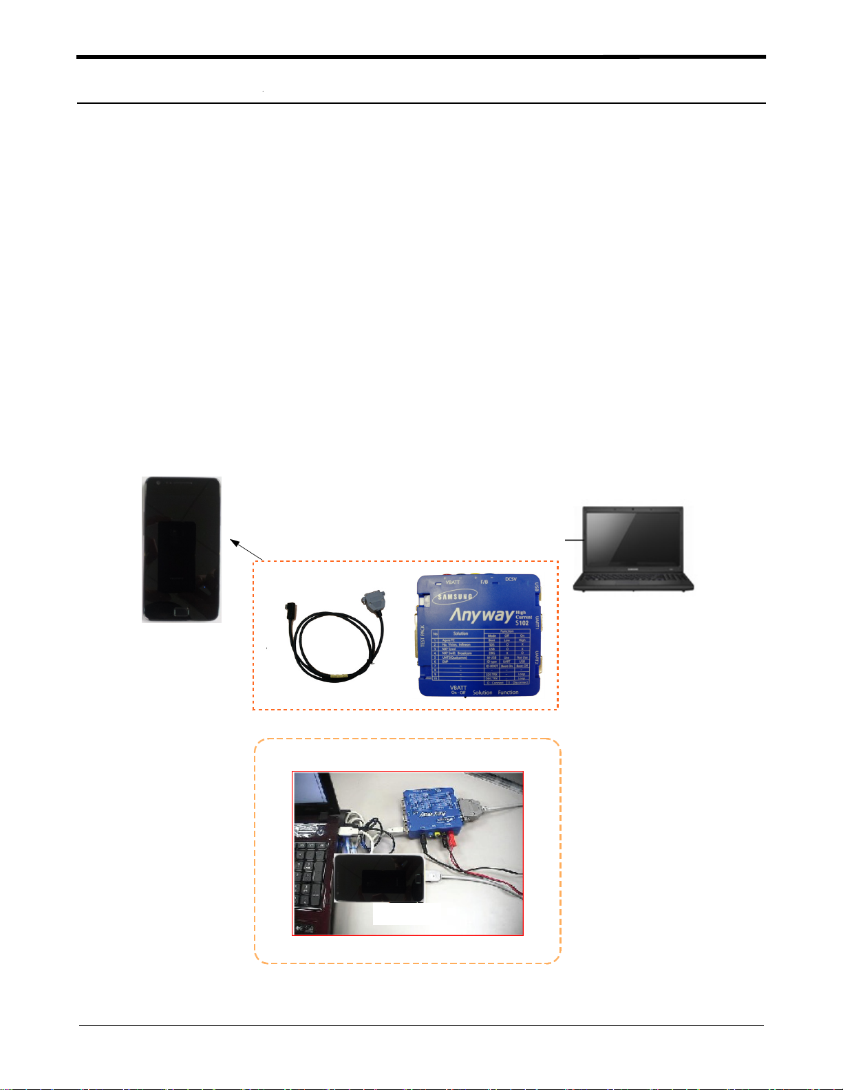
Required items in order to install S/W
Installation program: Downloader Program
GT-I9100 Mobile Phone
Data Cable
JIG BOX(GH99-36900B)
JIG Cable(GH39-01339A)
•
Adapter(GH99-38251A)
•
Serial Cable
•
Mobile device specific S/W: Binary files
Settings
※
Connect ANYWAY JIG BOX
with JIG CABLE(Phone to JIG)
or PC to Phone Using Data Cable
(Odin3 v1.83.exe)
6-5
Confidential and proprietary-the contents in this service guide subject to change without prior notice.
Distribution, transmission, or infringement of any content or data from this document without Samsung’swritten authorization is strictly prohibited.

Level6Repair
6-1-2.
S/W Installation Program(Downloader program)
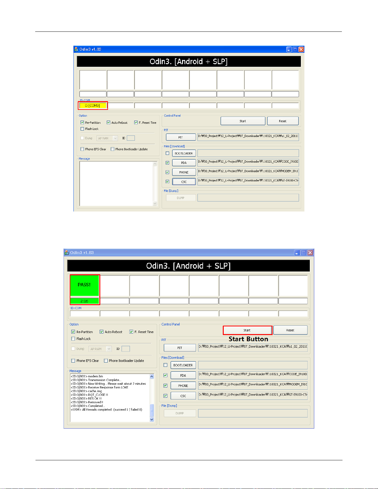
Open up the S/W Installation Program by executing the
Odin3 v1.83.exe"
"
Enable the check mark by click on the following options,
.
1
Check Re-Partition, Auto Reboot, and F. Reset Time
-
Check PIT
-
Check PDA, PHONE, and CSC Files
-
6-2
Confidential and proprietary-the contents in this service guide subject to change without prior notice.
Distribution, transmission, or infringement of any content or data from this document without Samsung’swritten authorization is strictly prohibited.
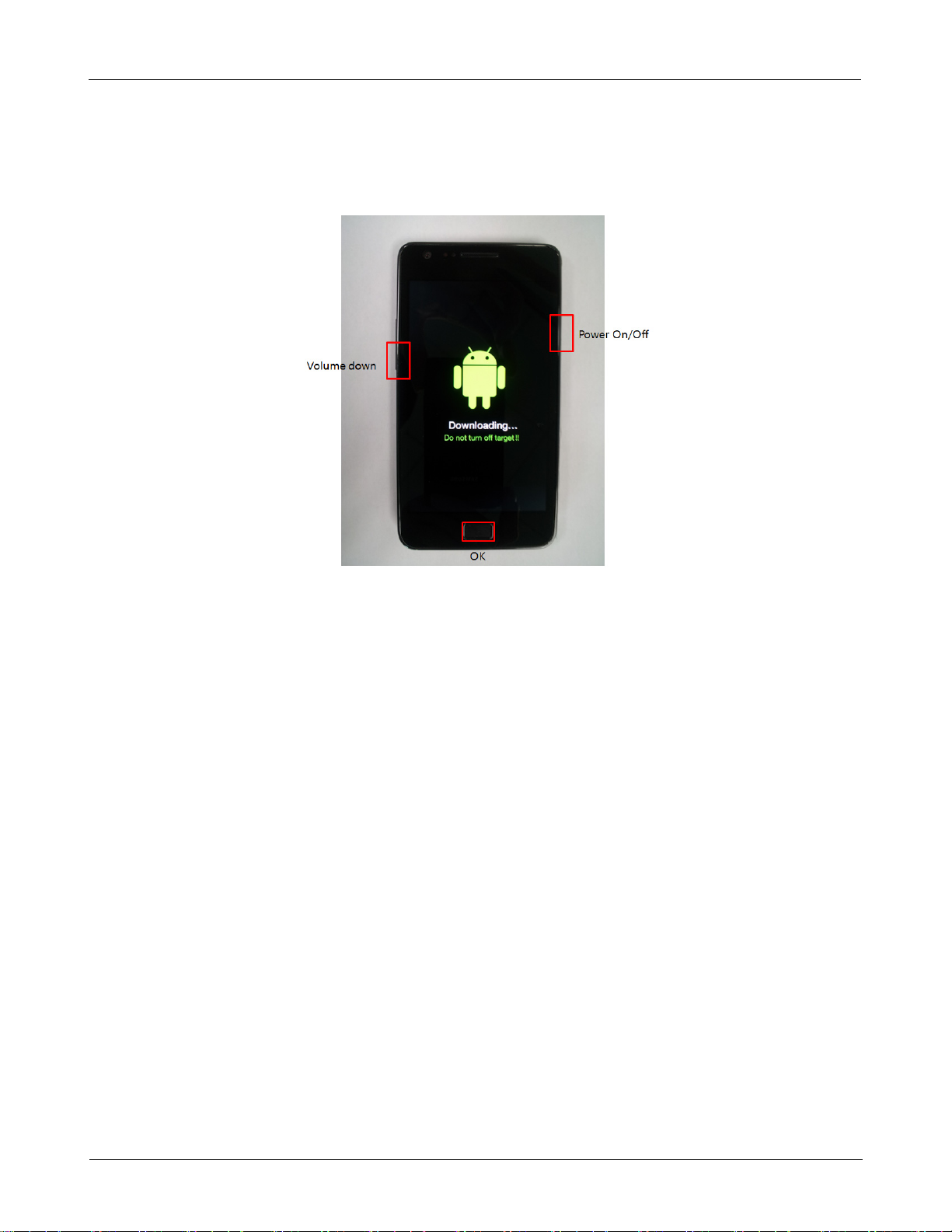
Enter into Download Mode
.
2
Enter into Download Mode by pressing Volume Down button, OK button, and
ON/OFF Button simultaneously.
Level6Repair
Connect the device to PC via Data Cable.
.
3
Make sure that the one of communication port[ID:COM] box is highlighted in
yellow. The device is now connected with the PC and ready to download the
binary file into the device.
6-3
Confidential and proprietary-the contents in this service guide subject to change without prior notice.
Distribution, transmission, or infringement of any content or data from this document without Samsung’swritten authorization is strictly prohibited.
Level6Repair
Start downloading binary file into the device by clicking Start Button on the screen.
.
4
the green colored"PASS!" sign will appear on the upper-left box if the binary file
has been successfully downloaded into the device.
6-4
Confidential and proprietary-the contents in this service guide subject to change without prior notice.
Distribution, transmission, or infringement of any content or data from this document without Samsung’swritten authorization is strictly prohibited.

Level6Repair
Disconnect the device from the Data cable.
5.
Once the device boots up, you can check the version of the binary file or name
.
6
by pressing the following code in sequence;
*#1234#
You can performfullreset by pressing the following code in sequence;
*2767*3855#
6-5
Confidential and proprietary-the contents in this service guide subject to change without prior notice.
Distribution, transmission, or infringement of any content or data from this document without Samsung’swritten authorization is strictly prohibited.

Reference Abbreviate
9.
Reference Abbreviate
AAC: AdvancedAudioCoding.
―
AVC: AdvancedVideoCoding.
―
BER: BitErrorRate
―
BPSK: BinaryPhaseShiftKeying
―
CA: ConditionalAccess
―
CDM: CodeDivisionMultiplexing
―
C/I: CarriertoInterference
―
DMB: DigitalMultimediaBroadcasting
―
EuropeanStandard
―두:
ES: ElementaryStream
―
ETSI: EuropeanTelecommunicationsStandardsInstitute
―
MPEG: MovingPictureExpertsGroup
―
PN: Pseudo-randomNoise
―
PS: PilotSymbol
―
QPSK: QuadraturePhaseShiftKeying
―
RS: Reed-Solomon
―
SI: ServiceInformation
―
TDM: TimeDivisionMultiplexing
―
TS: TransportStream
―
9-1
Confidential and proprietary-the contents in this service guide subject to change without prior notice.
Distribution, transmission, or infringement of any content or data from this document without Samsung’swritten authorization is strictly prohibited.

Safety Precautions
1.
1-1.
Repair Precaution
Before attempting any repair or detailed tuning, shield the device from RF noise or static
electricity discharges.
Use only demagnetized tools that are specifically designed for small electronic repairs,
as most electronic parts are sensitive to electromagnetic forces.
Use only high quality screwdrivers when servicing products. Low quality screwdrivers can
easily damage the heads of screws.
Use only conductor wire of the properly gauge and insulation for low resistance, because of
the low margin of error of most testing equipment.
We recommend
Hand-soldering is not recommended, because printed circuit boards(PCBs) can be easily
damaged, even with relatively low heat. Never useasoldering iron withapower rating of
more than 100 watts and use only lead-free solder with a melting point below 250°C (482°F).
gauge twisted copper wire.
22-
Prior to disassembling the battery charger for repair, ensure that the AC power is disconnected.
Always use the replacement parts that are registered in the SEC system. Third-party replac
ement parts may not function properly.
1-1
Confidential and proprietary-the contents in this service guide subject to change without prior notice.
Distribution, transmission, or infringement of any content or data from this document without Samsung’swritten authorization is strictly prohibited.

Safety Precautions
1-2.
ESD(Electrostatically Sensitive Devices) Precaution
Many semiconductors and ESDs in electronic devices are particularly sensitive to static discha
rge and can be easily damaged by it. We recommend protecting these components with cond
uctive anti-static bags when you store or transport them.
Always use an anti-static strap or wristband and remove electrostatic buildup or dissipate
static electricity from your body before repairing ESDs.
Ensure that soldering irons have AC adapter with ground wires and that the ground wires are
properly connected.
Use only desoldering tools with plastic tips to prevent static discharge.
Properly shield the work environment from accidental electrostatic discharge before opening
packages containing ESDs.
The potential for static electricity discharge may be increased in low humidity environments,
such as air-conditioned rooms. Increase the airflow to the working area to decrease the
chance of accidental static electricity discharges.
1-2
Confidential and proprietary-the contents in this service guide subject to change without prior notice.
Distribution, transmission, or infringement of any content or data from this document without Samsung’swritten authorization is strictly prohibited.
Exploded View and Parts List
4.
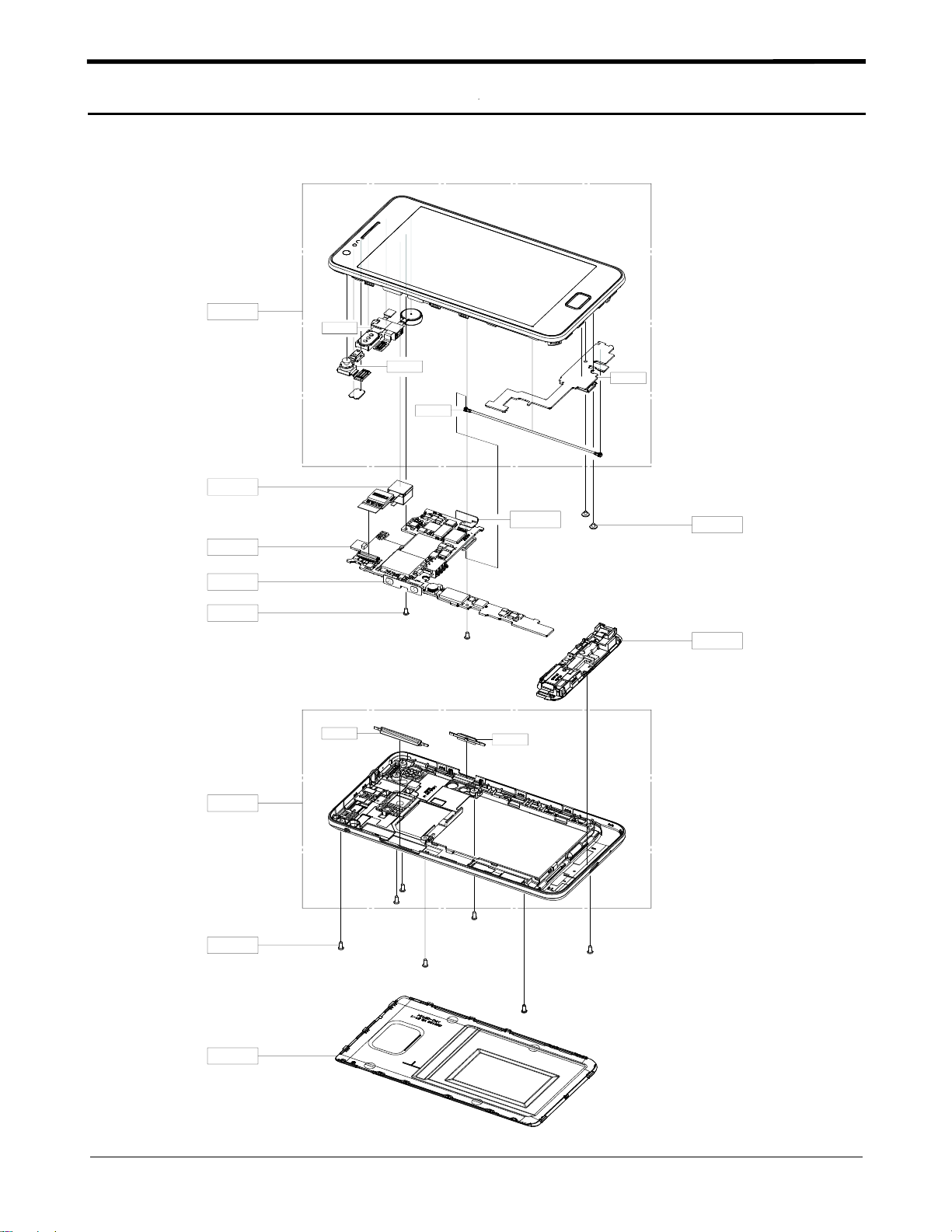
Cellular phone Exploded View
4-1.
QFR01
QCA01
QMP01
QVK01
QCR12
QAR01
QVO01
QCA02
QCB01
QCK01
QVK02
QME02
QCR96
QSP01
QRE01
QCR03
QBC00
4-1
Confidential and proprietary-the contents in this service guide subject to change without prior notice.
Distribution, transmission, or infringement of any content or data from this document without Samsung’swritten authorization is strictly prohibited.

Exploded View and Parts List
Cellular phone Parts list
4-2.
Design LOC Description SEC CODE
QCR12 SCREW-MACHINE
QCR03 SCREW-MACHINE
QCR96 SCREW-MACHINE
6001-001530
6001-001811
6001-002259
QVK02 KEY FPCB-POWER KEY(GT_9100) GH59-10916A
QSP01 MODULE-SPK+INT(GT_I9100) GH59-10917A
QVK01 KEY FPCB-VOLUME KEY(GT_9100) GH59-10921A
QMP01 A/S ASSY-PBA MAIN(COMM)GT_I9100 GH82-05732A
QCA01 ASSY CAMERA-MODULE,8M(GT_I9100) GH96-05139A
QBC00 ASSY COVER-BATT GH98-19595A
QFR01 MEA FRONT-OCTA LCD ASSY(OPEN) GH97-12175A
QCB01 CBF COAXIAL CABLE-75.5MM(GT_I9100) GH39-01475A
QAR01 MODULE-RCV+MOT+MIC+E/JACK FPCB(GT_I9100) GH59-10935A
QME02 ASSY ETC-SUB FPCB(GT_I9100) GH59-10949A
QCA02 CAMERA MODULE-GT-I9100_2M CAM GH59-10986A
QRE01 ASSY CASE-REAR GH98-19594A
QVO01 ASSY KEY-VOL GH98-19806A
QCK01 ASSY KEY-PWR GH98-19807A
4-2
Confidential and proprietary-the contents in this service guide subject to change without prior notice.
Distribution, transmission, or infringement of any content or data from this document without Samsung’swritten authorization is strictly prohibited.

MAIN Electrical Parts List
5.
SEC CODE Design LOC Description
0403-001688
0404-001245
0406-001446
0407-001002
0505-002388
0601-003079
0801-003024
0801-003031
0908-002766
1001-001481
1001-001635
1001-001699
1003-002100
1108-000424
1201-003139
1201-003217
1202-001068
1202-001118
1203-004339
1203-004802
1203-004819
1203-004819
1203-005044
1203-005244
1203-005574
1203-005580
1203-006651
1203-006794
1203-006801
1203-006802
1203-006847
1203-006851
1203-006884
1204-003167
1204-003171
1204-003176
D500 DIODE-ZENER
D501 DIODE-SCHOTTKY
ZD700,ZD701 DIODE-TVS
D502 DIODE-ARRAY
Q500 FET-SILICON
LED500 LED
U300 IC
U400 IC
UCP400 IC
U502 IC
U600 IC
U709 IC
U203 IC
UME300 IC
PAM200 IC
PAM100 IC
U706 IC
U603 IC
U704 IC
U707 IC
U609,U610,U611,U703 IC
U711,U720 IC
U702 IC
U710 IC
U701 IC
U206 IC
U718 IC
U503 IC
U104 IC
U103 IC
U303 IC
U501 IC
U504 IC
U601 IC
U202 IC
U205 IC
5-1
Confidential and proprietary-the contents in this service guide subject to change without prior notice.
Distribution, transmission, or infringement of any content or data from this document without Samsung’swritten authorization is strictly prohibited.

Main Electrical Parts List
SEC CODE Design LOC Description
1205-004174
1205-004195
1205-004213
1205-004233
1209-001997
1209-002041
1209-002045
1404-001221
1405-001183
1405-001183
2007-000143
2007-007107
2007-007133
2007-007137
2007-007312
2007-007468
2007-007488
2007-007517
2007-007741
2007-007942
2007-008040
2007-008045
2007-008048
2007-008052
2007-008052
2007-008052
2007-008055
2007-008055
2007-008055
2007-008055
2007-008055
2007-008296
2007-008312
2007-008391
2007-008403
2007-008419
U602 IC
U100 IC
UCP300 IC
U708 IC
U607 IC
U608 IC
U606 IC
TH300,TH400,TH401 THERMISTOR
VR600,VR602,VR603 VARISTOR
VR604,VR605,VR607 VARISTOR
R421,R422 R-CHIP
R322 R-CHIP
R529,R531 R-CHIP
R446 R-CHIP
R474,R475 R-CHIP
R527 R-CHIP
R525 R-CHIP
R425,R428,R472,R473 R-CHIP
R515,R516 R-CHIP
R625 R-CHIP
R603,R604 R-CHIP
R704 R-CHIP
R730,R731 R-CHIP
R312,R408,R409,R410 R-CHIP
R411,R464,R468,R469 R-CHIP
R517,R722 R-CHIP
R341,R429,R431,R432 R-CHIP
R434,R438,R456,R457 R-CHIP
R459,R460,R461,R501 R-CHIP
R528,R530,R546,R605,R619 R-CHIP
R711 R-CHIP
R524 R-CHIP
R348,R626 R-CHIP
R532 R-CHIP
R514 R-CHIP
R216,R308,R309,R423 R-CHIP
5-2
Confidential and proprietary-the contents in this service guide subject to change without prior notice.
Distribution, transmission, or infringement of any content or data from this document without Samsung’swritten authorization is strictly prohibited.

Main Electrical Parts List
SEC CODE Design LOC Description
2007-008419
2007-008419
2007-008419
2007-008419
2007-008420
2007-008420
2007-008420
2007-008465
2007-008483
2007-008483
2007-008486
2007-008502
2007-008516
2007-008516
2007-008516
2007-008516
2007-008516
2007-008516
2007-008516
2007-008516
2007-008531
2007-008531
2007-008579
2007-008588
2007-008588
2007-008800
2007-009084
2007-009111
2007-009155
2007-009157
2007-009157
2007-009158
2007-009171
2007-009171
2007-009212
2007-009315
R424,R426,R427,R454 R-CHIP
R455,R466,R467,R477 R-CHIP
R478,R609,R611,R615 R-CHIP
R616 R-CHIP
R214,R215,R351,R479 R-CHIP
R480,R523,R600,R623 R-CHIP
R734,R735,R737 R-CHIP
R533 R-CHIP
R300,R301,R302,R303 R-CHIP
R305 R-CHIP
R710 R-CHIP
R526 R-CHIP
R203,R210,R211,R232 R-CHIP
R304,R323,R325,R404 R-CHIP
R405,R406,R448,R449 R-CHIP
R450,R463,R465,R508 R-CHIP
R509,R510,R511,R513 R-CHIP
R617,R618,R628,R702 R-CHIP
R715,R721,R725,R729 R-CHIP
R732 R-CHIP
R201,R420,R629,R630 R-CHIP
R703 R-CHIP
R208 R-CHIP
R337,R338,R339,R470 R-CHIP
R471 R-CHIP
R433,R440 R-CHIP
R602,R709,R712,R713 R-CHIP
R346,R633,R634 R-CHIP
R350 R-CHIP
R349,R402,R403,R441 R-CHIP
R481,R482 R-CHIP
R727,R728 R-CHIP
R313,R314,R315,R316 R-CHIP
R317,R318,R319,R320 R-CHIP
R622 R-CHIP
R344 R-CHIP
5-3
Confidential and proprietary-the contents in this service guide subject to change without prior notice.
Distribution, transmission, or infringement of any content or data from this document without Samsung’swritten authorization is strictly prohibited.

Main Electrical Parts List
SEC CODE Design LOC Description
2007-009408
2007-009801
2007-009964
2007-009969
2007-010029
2007-010202
2007-010233
2203-000233
2203-000725
2203-005138
2203-005281
2203-005446
2203-005682
2203-005682
2203-005682
2203-005717
2203-005725
2203-005726
2203-005729
2203-005729
2203-005731
2203-005734
2203-005736
2203-005779
2203-005789
2203-005806
2203-006048
2203-006194
2203-006208
2203-006260
2203-006305
2203-006324
2203-006348
2203-006379
2203-006399
2203-006423
R414,R415,R701 R-CHIP
R101,R102 R-CHIP
R442,R444 R-CHIP
R624 R-CHIP
R418 R-CHIP
R204,R205,R206,R207 R-CHIP
R330 R-CHIP
C219 C-CERAMIC,CHIP
C557 C-CERAMIC,CHIP
C441,C447 C-CERAMIC,CHIP
C223 C-CERAMIC,CHIP
C201 C-CERAMIC,CHIP
C107,C124,C125,C126 C-CERAMIC,CHIP
C181,C346,C347,C348 C-CERAMIC,CHIP
L102 C-CERAMIC,CHIP
C102,C752,C758,C759 C-CERAMIC,CHIP
C439,C440 C-CERAMIC,CHIP
C100,C101,C129 C-CERAMIC,CHIP
C355,C520,C529,C613 C-CERAMIC,CHIP
C614,C639 C-CERAMIC,CHIP
C354 C-CERAMIC,CHIP
C637,C640 C-CERAMIC,CHIP
C220,C265 C-CERAMIC,CHIP
C217,C218 C-CERAMIC,CHIP
L106 C-CERAMIC,CHIP
C113 C-CERAMIC,CHIP
C448,C644 C-CERAMIC,CHIP
C121,C302,C305,C641 C-CERAMIC,CHIP
C531,C533,C534,C535 C-CERAMIC,CHIP
C162 C-CERAMIC,CHIP
C442 C-CERAMIC,CHIP
C567 C-CERAMIC,CHIP
C504,C566 C-CERAMIC,CHIP
C109 C-CERAMIC,CHIP
C656 C-CERAMIC,CHIP
C136,C137,C140,C141 C-CERAMIC,CHIP
5-4
Confidential and proprietary-the contents in this service guide subject to change without prior notice.
Distribution, transmission, or infringement of any content or data from this document without Samsung’swritten authorization is strictly prohibited.

Main Electrical Parts List
SEC CODE Design LOC Description
2203-006423
2203-006423
2203-006423
2203-006423
2203-006423
2203-006423
2203-006423
2203-006423
2203-006423
2203-006423
2203-006423
2203-006423
2203-006423
2203-006423
2203-006474
2203-006556
2203-006562
2203-006562
2203-006562
2203-006562
2203-006562
2203-006611
2203-006642
2203-006647
2203-006647
2203-006648
2203-006668
2203-006707
2203-006815
2203-006824
2203-006839
2203-006839
2203-006839
2203-006839
2203-006841
2203-006872
C142,C144,C145,C146 C-CERAMIC,CHIP
C147,C148,C163,C215 C-CERAMIC,CHIP
C216,C300,C303,C306 C-CERAMIC,CHIP
C307,C313,C314,C326 C-CERAMIC,CHIP
C328,C329,C330,C331 C-CERAMIC,CHIP
C334,C335,C337,C338 C-CERAMIC,CHIP
C339,C342,C343,C344 C-CERAMIC,CHIP
C359,C405,C409,C412 C-CERAMIC,CHIP
C414,C416,C419,C424 C-CERAMIC,CHIP
C443,C445,C446,C540 C-CERAMIC,CHIP
C559,C607,C610,C643 C-CERAMIC,CHIP
C647,C715,C716,C727 C-CERAMIC,CHIP
C728,C731,C734,C737 C-CERAMIC,CHIP
C741 C-CERAMIC,CHIP
C351,C353 C-CERAMIC,CHIP
C760,C761 C-CERAMIC,CHIP
C135,C173,C211,C213 C-CERAMIC,CHIP
C254,C356,C357,C358 C-CERAMIC,CHIP
C501,C502,C516,C518 C-CERAMIC,CHIP
C713,C723,C746,C757 C-CERAMIC,CHIP
C764 C-CERAMIC,CHIP
C120 C-CERAMIC,CHIP
C404,C407 C-CERAMIC,CHIP
C143,C149,C150,C151 C-CERAMIC,CHIP
C166,C624,C626 C-CERAMIC,CHIP
C122,C621,C622 C-CERAMIC,CHIP
C410,C411,C611,C612 C-CERAMIC,CHIP
C127 C-CERAMIC,CHIP
C112,C114 C-CERAMIC,CHIP
C179,C180 C-CERAMIC,CHIP
C117,C138,C157,C158 C-CERAMIC,CHIP
C208,C253,C255,C517 C-CERAMIC,CHIP
C519,C562,C605,C655 C-CERAMIC,CHIP
C657,C659 C-CERAMIC,CHIP
C571 C-CERAMIC,CHIP
C139,C159,C160,C175 C-CERAMIC,CHIP
5-5
Confidential and proprietary-the contents in this service guide subject to change without prior notice.
Distribution, transmission, or infringement of any content or data from this document without Samsung’swritten authorization is strictly prohibited.

Main Electrical Parts List
SEC CODE Design LOC Description
2203-006872
2203-006872
2203-006872
2203-006872
2203-006872
2203-006872
2203-006890
2203-006979
2203-006979
2203-007133
2203-007194
2203-007210
2203-007210
2203-007210
2203-007210
2203-007210
2203-007270
2203-007270
2203-007271
2203-007271
2203-007271
2203-007279
2203-007317
2203-007317
2203-007391
2203-007393
2203-007393
2203-007393
2203-007393
2203-007393
2203-007449
2203-007449
2203-007449
2203-007449
2203-007449
2203-007449
C202,C209,C210,C266 C-CERAMIC,CHIP
C301,C308,C542,C545 C-CERAMIC,CHIP
C547,C548,C551,C552 C-CERAMIC,CHIP
C553,C623,C704,C718 C-CERAMIC,CHIP
C719,C726,C730,C733 C-CERAMIC,CHIP
C736 C-CERAMIC,CHIP
C530,C645,C646 C-CERAMIC,CHIP
C103,C116,C214,C318 C-CERAMIC,CHIP
C558,C627,C630 C-CERAMIC,CHIP
C720,C753,C754 C-CERAMIC,CHIP
C241 C-CERAMIC,CHIP
C164,C176,C304,C310 C-CERAMIC,CHIP
C315,C319,C324,C327 C-CERAMIC,CHIP
C332,C336,C340,C341 C-CERAMIC,CHIP
C345,C360,C511,C632 C-CERAMIC,CHIP
C633 C-CERAMIC,CHIP
C155,C156,C262,C724 C-CERAMIC,CHIP
C725 C-CERAMIC,CHIP
C167,C408,C413,C415 C-CERAMIC,CHIP
C418,C430,C438,C601 C-CERAMIC,CHIP
C706,C707,C708,C717 C-CERAMIC,CHIP
C309,C320,C539 C-CERAMIC,CHIP
C172,C178,C417,C420 C-CERAMIC,CHIP
C425,C427,C435 C-CERAMIC,CHIP
C573,C642 C-CERAMIC,CHIP
C134,C169,C506,C507 C-CERAMIC,CHIP
C508,C509,C510,C521 C-CERAMIC,CHIP
C522,C523,C524,C525 C-CERAMIC,CHIP
C526,C527,C537,C701 C-CERAMIC,CHIP
C762 C-CERAMIC,CHIP
C174,C321,C322,C323 C-CERAMIC,CHIP
C325,C333,C349,C350 C-CERAMIC,CHIP
C400,C401,C402,C403 C-CERAMIC,CHIP
C406,C421,C422,C423 C-CERAMIC,CHIP
C426,C428,C429,C432 C-CERAMIC,CHIP
C433,C436,C437,C500 C-CERAMIC,CHIP
5-6
Confidential and proprietary-the contents in this service guide subject to change without prior notice.
Distribution, transmission, or infringement of any content or data from this document without Samsung’swritten authorization is strictly prohibited.

Main Electrical Parts List
SEC CODE Design LOC Description
2203-007449
2203-007449
2203-007449
2203-007449
2203-007449
2203-007449
2203-007449
2203-007449
2203-007449
2203-007449
2203-007449
2203-007701
2203-007701
2203-007781
2203-007840
2404-001496
2404-001506
2409-001127
2409-001166
2703-000213
2703-001231
2703-001285
2703-001750
2703-002199
2703-002313
2703-002596
2703-002901
2703-002907
2703-002955
2703-002958
2703-002961
2703-003004
2703-003476
2703-003545
2703-003686
2703-003755
C541,C543,C544,C546 C-CERAMIC,CHIP
C549,C550,C554,C555 C-CERAMIC,CHIP
C556,C572,C600,C602 C-CERAMIC,CHIP
C603,C604,C606,C608 C-CERAMIC,CHIP
C609,C615,C617,C618 C-CERAMIC,CHIP
C625,C628,C629,C631 C-CERAMIC,CHIP
C658,C660,C703,C705 C-CERAMIC,CHIP
C709,C710,C711,C712 C-CERAMIC,CHIP
C714,C739,C742,C744 C-CERAMIC,CHIP
C747,C748,C755,C756 C-CERAMIC,CHIP
C763,C765 C-CERAMIC,CHIP
C171,C311,C312,C431 C-CERAMIC,CHIP
C505,C532,C538 C-CERAMIC,CHIP
C564,C565 C-CERAMIC,CHIP
C206 C-CERAMIC,CHIP
TA600 C-TA,CHIP
TA501,TA502,TA503 C-TA,CHIP
C168 C-POLYMER,CHIP
BAT500 C-EDL
L201 INDUCTOR-SMD
L509 INDUCTOR-SMD
L606 INDUCTOR-SMD
C104 INDUCTOR-SMD
L206 INDUCTOR-SMD
C203 INDUCTOR-SMD
L120,L127 INDUCTOR-SMD
C132 INDUCTOR-SMD
L114 INDUCTOR-SMD
C118 INDUCTOR-SMD
C130,C133,L113 INDUCTOR-SMD
L200,L205 INDUCTOR-SMD
L207 INDUCTOR-SMD
L211 INDUCTOR-SMD
L202 INDUCTOR-SMD
L503 INDUCTOR-SMD
L119,L121,L122 INDUCTOR-SMD
5-7
Confidential and proprietary-the contents in this service guide subject to change without prior notice.
Distribution, transmission, or infringement of any content or data from this document without Samsung’swritten authorization is strictly prohibited.

Main Electrical Parts List
SEC CODE Design LOC Description
2703-003770
2703-003869
2703-003892
2703-003897
2703-003909
2703-003911
2703-004000
2703-004012
2703-004034
2703-004035
2703-004038
2703-004039
2703-004052
2801-004339
2801-004458
2801-005051
2809-001348
2809-001369
2901-001413
2901-001413
2901-001625
2901-001647
2910-000125
2911-000166
3301-001729
3301-001876
3301-001885
3301-001912
3301-001929
3301-001956
3301-002062
3301-002065
3301-002065
3301-002066
3301-002078
3705-001448
L703 INDUCTOR-SMD
L302,L303 INDUCTOR-SMD
L504 INDUCTOR-SMD
L704 INDUCTOR-SMD
L501,L502,L506 INDUCTOR-SMD
L118,L500,L508 INDUCTOR-SMD
L107 INDUCTOR-SMD
C128,L110 INDUCTOR-SMD
L103,L104 INDUCTOR-SMD
L109 INDUCTOR-SMD
C111 INDUCTOR-SMD
L117 INDUCTOR-SMD
L507 INDUCTOR-SMD
OSC300,OSC500 CRYSTAL-SMD
OSC400 CRYSTAL-SMD
OSC201 CRYSTAL-SMD
OSC200 OSCILLATOR-VCTCXO
OSC100 OSCILLATOR-VCTCXO
F700,F701,F702,F704 FILTER-EMI SMD
F707,F709 FILTER-EMI SMD
F706 FILTER-EMI SMD
F703,F705 FILTER-EMI SMD
F100 DUPLEXER-SAW
U101 DUPLEXER-SAW
L705,L706,L707,L708 BEAD-SMD
L209,L210 BEAD-SMD
L213 BEAD-SMD
L212 BEAD-SMD
L601 BEAD-SMD
L300,L301 BEAD-SMD
L116 BEAD-SMD
L204,L600,L607,L608 BEAD-SMD
L609,L614 BEAD-SMD
L700,L701,L702 BEAD-SMD
L602,L604 BEAD-SMD
ANT100 CONNECTOR-COAXIAL
5-8
Confidential and proprietary-the contents in this service guide subject to change without prior notice.
Distribution, transmission, or infringement of any content or data from this document without Samsung’swritten authorization is strictly prohibited.

Main Electrical Parts List
SEC CODE Design LOC Description
3705-001731
3708-002162
3709-001575
3709-001626
3711-006483
3711-006925
3711-007173
3711-007295
3711-007806
3711-007810
3712-001348
4709-001987
RFS100 CONNECTOR-COAXIAL
HDC700 CONNECTOR-FPC
CD300 CONNECTOR-CARD EDGE
SIM300 CONNECTOR-CARD EDGE
HDC701 HEADER-BOARD TO BOARD
HDC704 HEADER-BOARD TO BOARD
HDC702 HEADER-BOARD TO BOARD
HDC703 HEADER-BOARD TO BOARD
BTC500 HEADER-BATTERY
HDC600 HEADER-BOARD TO BOARD
ANT200,ANT201 CONNECTOR-TERMINAL
MOD201 IC
GH62-00015A PORON202 PAD GAP-PCB GASKET
GH70-0
GH70-0
GH70-0
GH70-0
GH70-0
GH70-0
GH70-0
7467A
7467A
7467A
7467A
7467A
7467A
7467A
SC100,SC101,SC102 ICT SHIELD-CAN CLIP
SC103,SC104,SC105 ICT SHIELD-CAN CLIP
SC107,SC109,SC110 ICT SHIELD-CAN CLIP
SC111,SC112,SC113 ICT SHIELD-CAN CLIP
SC114,SC115,SC116 ICT SHIELD-CAN CLIP
SC117,SC118,SC119 ICT SHIELD-CAN CLIP
SC120,SC121,SC122 ICT SHIELD-CAN CLIP
GH80-03320A R353 Solder Bridge PAD
GH80-03321A C651,R
GH80-03321A
R329,R331,R719,R720
212,R310,R328
Solder Bridge PAD
Solder Bridge PAD
GH80-03321A R741 Solder Bridge PAD
5-9
Confidential and proprietary-the contents in this service guide subject to change without prior notice.
Distribution, transmission, or infringement of any content or data from this document without Samsung’swritten authorization is strictly prohibited.
7.
7-1.
Level
2
Disassembly
Repair
1
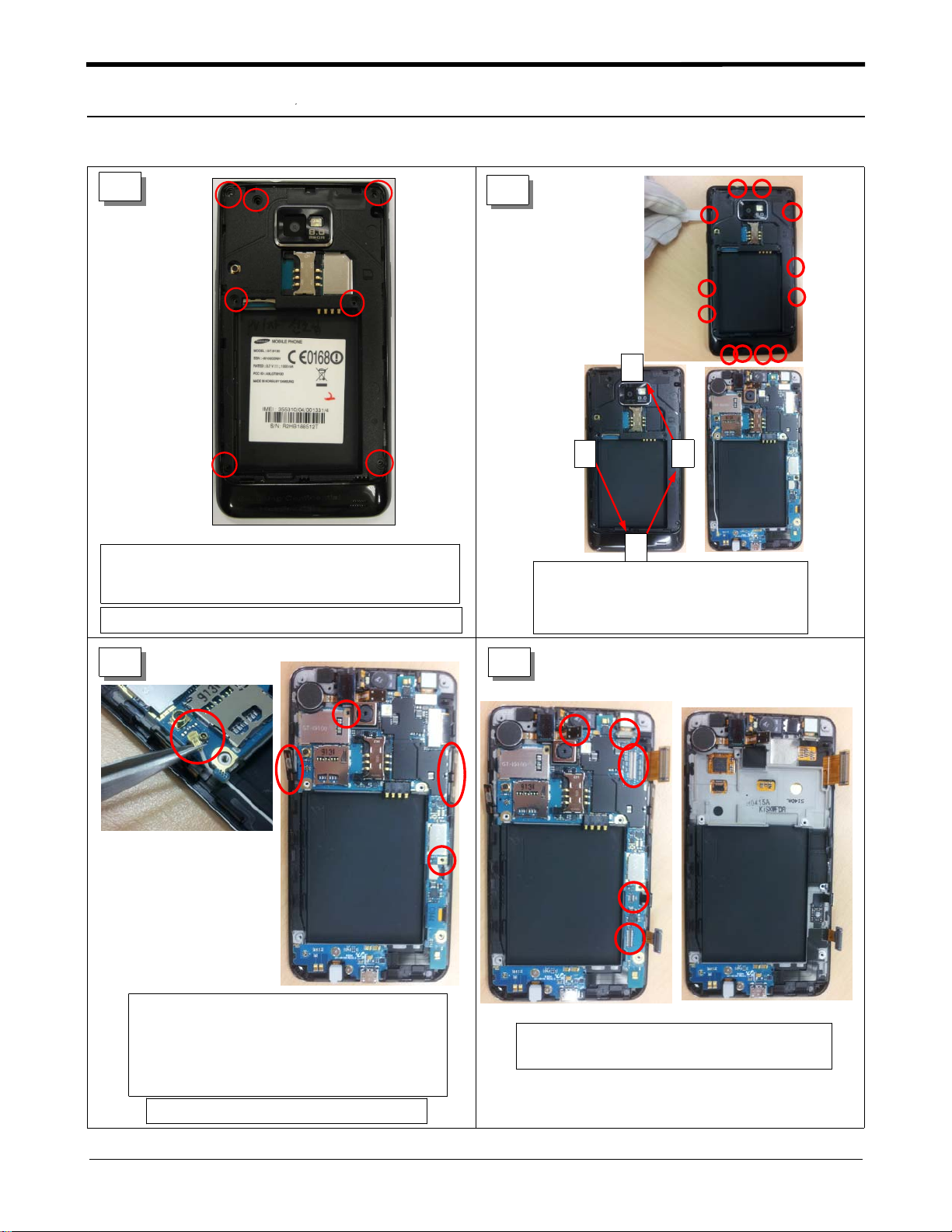
Carefully release the screws at7different locations
from the rear cover.
Torque:
(
1.1±0.1
Be careful not to scratch rear cover.
kgf.cm)(Size: M1.4*L3)
2
4
1
3
2
Disengage the rear cover from
the front cover by using the hook
at12points that colored in red
Follow the numbered sequence
(
when you disjoint)
3
Separate the coaxial cable of antenna
assembly from the PBA.
Release the screw at2points(Size: M1.4*L3)
Torque:
(
Detach the side FPCBs from the Bracket.
1.1±0.1
Be careful not to damage the FPCBs.
kgf.cm)
4
Separate all connector ribbons from the PBA.
Separate the PBA from the Front.
7-1
Confidential and proprietary-the contents in this service guide subject to change without prior notice.
Distribution, transmission, or infringement of any content or data from this document without Samsung’swritten authorization is strictly prohibited.
Level2Repair
7.
5 6
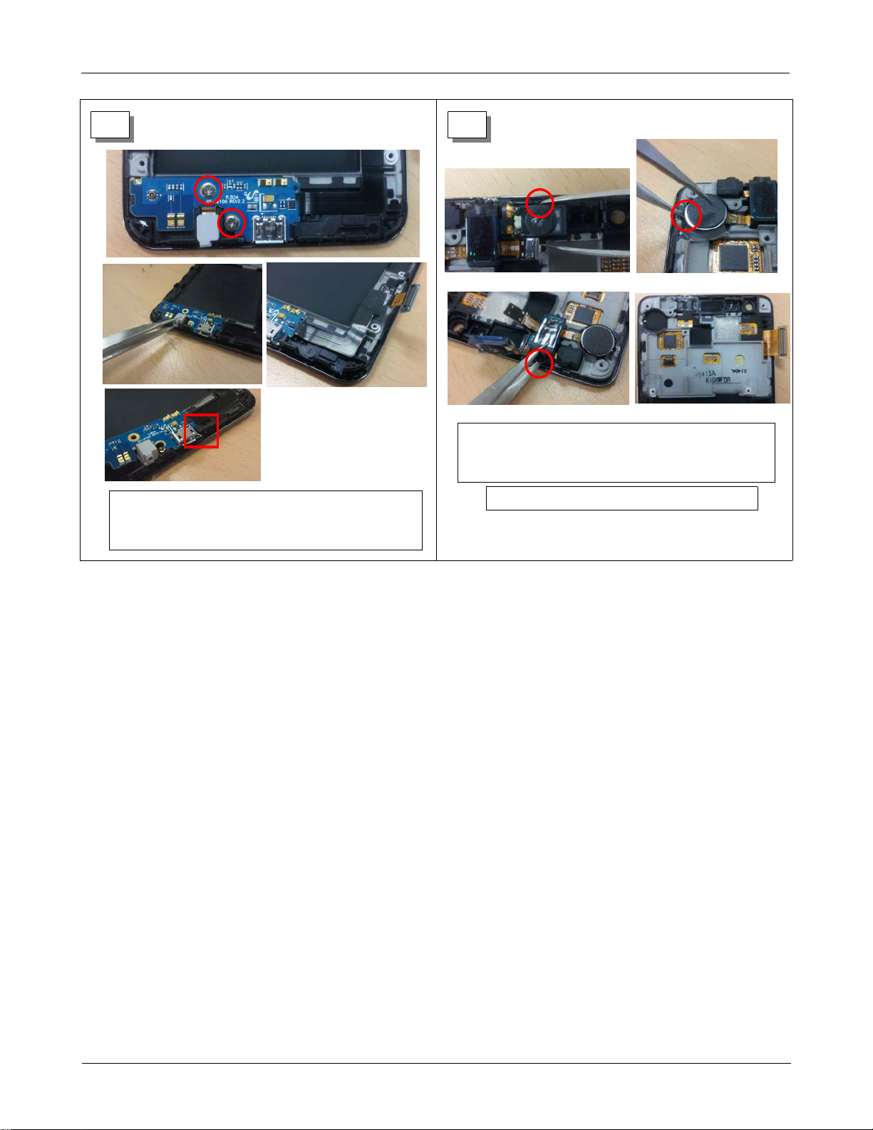
Separate the Receiver assembly from the Front.
Insertalong nose tweezer into the holes for
(
easy separation.
)
Release the screw at2point
Torque:
(
1.1±0.1
kgf.cm)
Size: M1.4*L2)
s (
Separate the sub PBA from the PBA.
Be careful not to damage the FPCBs.
7-2
Confidential and proprietary-the contents in this service guide subject to change without prior notice.
Distribution, transmission, or infringement of any content or data from this document without Samsung’swritten authorization is strictly prohibited.
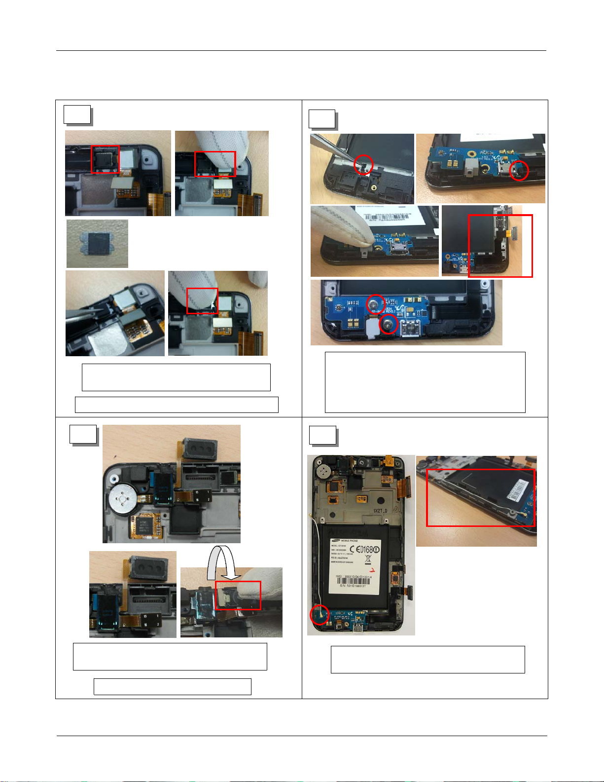
7-2.
Assembly
Level2Repair
7.
1
Insert the VGA Ass'y in the Front.
Put the chassis on the sensor.
Be careful not to damage the camera FPCB.
2
Attach the FPCB on the Front.
Insert the sub PBA in the hook.
Attach the FPCB on the Front.
Screw2points.(Size: M1.4*L2)
Torque:
(
1.1±0.1
kgf.cm)
3
Put the Receiver Ass'y on the Front.
Furl the Receiver and put it on the Front.
Be careful to damage the FPCB.
4
Connect the cable on the sub PBA.
Organize the cable on the Front
7-3
Confidential and proprietary-the contents in this service guide subject to change without prior notice.
Distribution, transmission, or infringement of any content or data from this document without Samsung’swritten authorization is strictly prohibited.
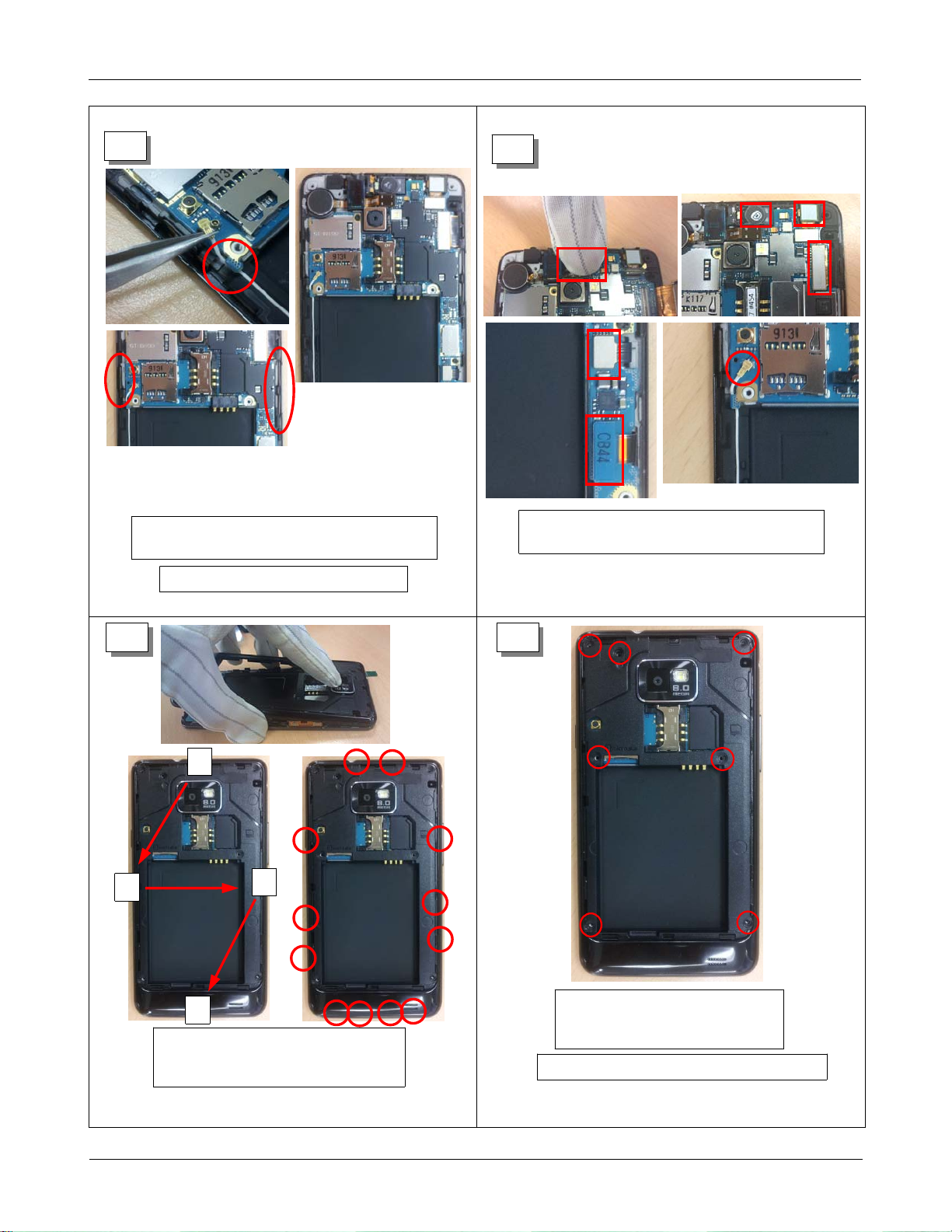
Level2Repair
7.
5
Put the PBA on the Front.
Attach the side FPCBs on the Bracket.
Be careful to damage the cable.
6
Connect all the connector on the PBA.
Connect the cable on the PBA.
7
1
2
3
4
Assemble the Rear and the Front.
Follow the order)
(
Hook at the12points.
8
Screw at7points.
Torque:
(
Size: M1.4*L3)
(
Be careful not to scratch rear cover.
1.1±0.1
kgf.cm)
7-4
Confidential and proprietary-the contents in this service guide subject to change without prior notice.
Distribution, transmission, or infringement of any content or data from this document without Samsung’swritten authorization is strictly prohibited.
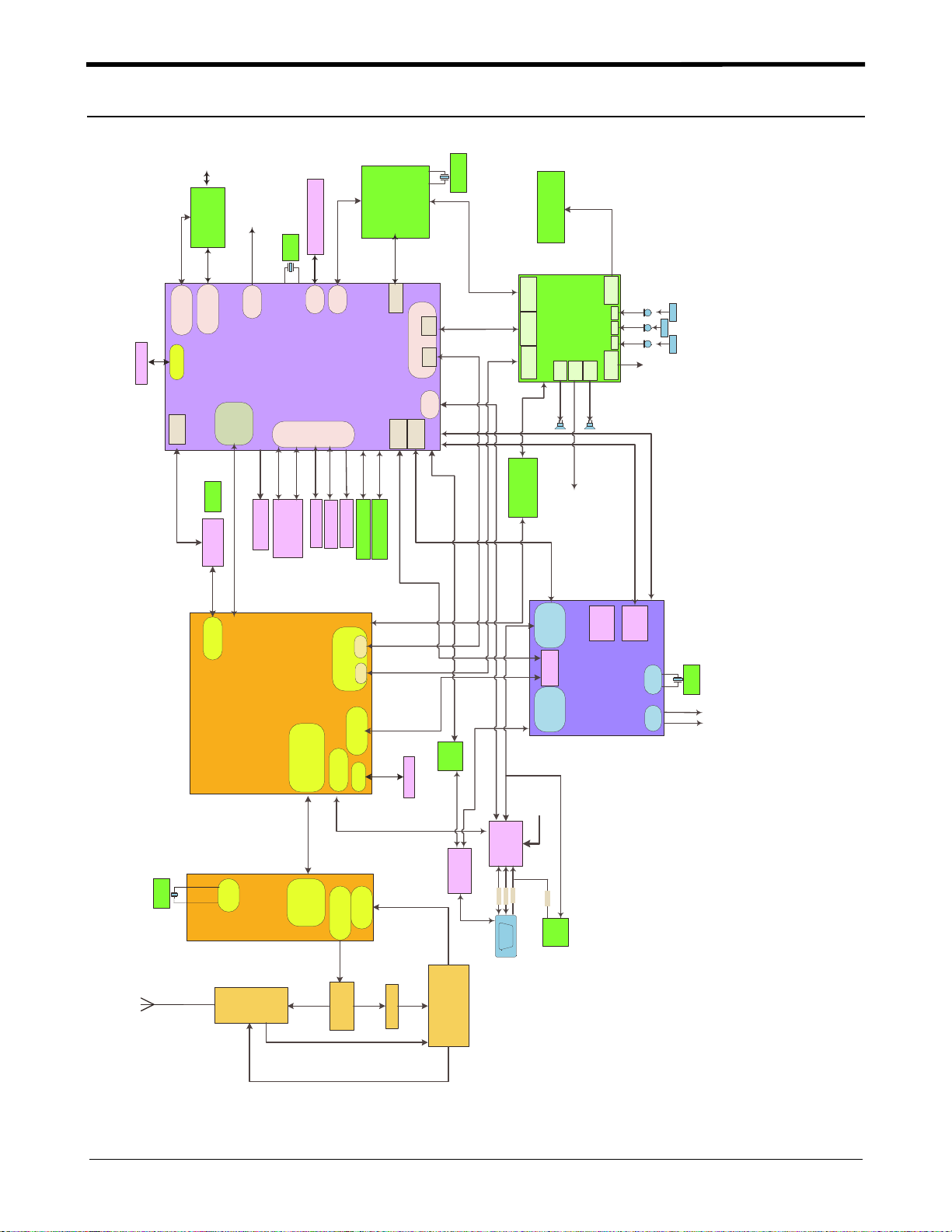
Level
8.
Block Diagram
8-1.
H
S
A
L
F
T
Repair
3
z
M
8
i
f
e
i
2
S
2
I
1
S
2
I
T
R
A
U
M
I
S
x
R
G
3
/
G
2
3G_LB
3G_HB
C
I
r
e
g
r
a
h
C
l
u
W
d
/
o
T
B
M
D
S
D
T
X
X
T
C
R
_
_
_
T
T
T
R
R
R
A
A
A
U
U
U
_
_
_
T
T
T
B
B
B
0
T
R
A
U
3
T
R
A
U
G
T
O
_
B
V
V
8
8
.
.
S
2
2
_
_
D
D
U
X
X
T
R
_
_
M
M
L
L
F
F
_
_
P
P
A
A
REC_PCM_CLK
REC_PCM_IN
REC_PCM_OUT
REC_PCM_SYNC
SPEECH_PCM_CLK
SPEECH_PCM_IN
SPEECH_PCM_OUT
SPEECH_PCM_SYNC
+
W
/
S
3G_TX
D
N
A
B
S
T
R
_
T
R
A
U
_
T
B
D
D
X
X
T
R
_
_
P
P
C
C
_
D
_
D
d
n
a
n
i
V
8
.
2
_
L
C
S
_
M
A
C
_
T
V
V
8
.
2
_
A
D
S
_
M
A
C
_
T
V
R
E
V
I
E
C
S
N
A
R
T
z
O
H
X
M
C
4
T
2
y
r
o
m
e
M
+
V
V
8
8
.
.
2
2
_
_
L
A
C
D
S
S
_
_
S
S
L
L
A
A
_
_
S
S
P
P
r
o
A
s
n
R
e
E
s
M
Y
A
X
C
O
T
R
V
P
/
C
I
M
P
P
C
+
P
C
2G_TX_LB
2G_TX_HB
v
o
M
/
i
G
V
6
8
.
1
2
i
F
i
W
)
V
8
.
2
(
3
C
1
C
/
M
M
0
M
M
)
P
O
P
(
O
I
P
G
V
V
V
V
8
8
.
.
8
8
.
.
2
2
2
2
_
_
_
_
L
A
L
A
C
D
C
D
S
S
S
S
_
_
_
_
H
H
E
E
C
C
S
S
U
U
N
N
O
O
E
E
T
T
S
S
R
Y
O
E
R
S
K
O
O
N
H
R
S
E
Y
C
N
S
U
E
G
C
S
O
C
T
A
O
I
D
U
A
e
c
a
f
r
e
t
n
i
F
R
B
l
S
a
t
U
i
g
i
D
F
R
l
x
a
T
t
i
g
G
i
3
D
/
G
2
H
L
_
_
M
M
P
P
M
A
P
G
3
/
G
2
P
S
V
V
I
8
8
.
.
2
2
_
_
L
A
C
D
S
S
_
_
M
M
A
A
C
C
_
_
A
A
G
G
E
E
M
M
I
O
P
I
I
P
M
G
H
S
A
L
F
T
1
T
R
A
U
D
S
S
D
T
T
X
X
T
R
C
R
_
_
_
_
T
T
T
T
R
R
R
R
A
A
A
A
U
U
U
U
_
_
_
_
S
S
S
S
P
P
P
P
G
G
G
G
z
H
M
6
2
)
V
8
.
1
(
F
T
I
I
B
B
4
G
2
R
F
I
D
C
L
r
o
s
s
e
c
o
r
P
n
o
i
t
a
c
i
l
p
)
p
Y
G
1
R
/
P
P
A
O
G
C
O
M
4
P
/
M
E
G
M
4
(
z
H
M
6
2
C
F
I
I
R
T
T
O
I
E
B
r
e
v
e
i
c
e
r
S
P
G
e
c
S
a
f
P
r
e
G
t
n
i
S
-
N
6
N
1
G
E
Y
A
R
S
O
M
M
E
M
l
o
r
C
t
S
n
o
O
c
M
S
A
H
L
A
M
T
4
-
.
7
X
3
T
C
U
N
K
N
L
I
O
Y
C
D
D
S
_
_
_
_
M
M
M
M
C
C
C
C
P
P
P
P
_
_
_
_
T
T
T
T
B
B
B
B
M
I
M
_
2
O
S
D
0
S
2
I
O
I
D
U
A
1
S
2
I
B
S
U
2
T
R
A
U
D
D
X
X
T
R
_
_
M
M
L
L
F
F
_
_
P
P
A
A
D
R
A
C
M
I
S
P
C
P
C
_
M
I
M
_
2
I
S
D
_
_
M
I
M
2
S
S
_
C
Y
N
L
M
K
C
I
_
M
_
2
S
C
2
I
_
L
H
M
_
R
O
S
N
E
S
M
/
C
2
I
_
L
H
M
V
V
8
8
.
.
1
1
_
_
D
D
X
X
T
R
_
_
P
P
C
C
-
/
+
L
D
H
_
M
M
P
D
/
A
P
D
_
C
I
M
P
D
I
/
P
D
/
M
D
_
L
H
M
C
I
h
c
t
i
w
S
P
D
_
B
S
U
M
D
/
P
D
_
B
S
U
X
R
K
N
A
B
W
A
S
/
P
U
D
o
i
d
a
R
M
F
S
3
2
t
I
r
/
o
P
M
C
F
I
P
S
1
2
t
I
r
/
o
P
M
C
F
I
P
S
2
2
t
I
r
/
o
P
M
P
K
C
F
I
P
M
P
S
A
_
T
U
P
N
O
_
_
/
T
T
N
I
U
U
_
O
O
M
_
_
C
K
K
P
P
P
_
S
S
H
C
C
E
E
D
E
O
P
S
C
p
i
h
C
C
I
M
2
D
D
X
X
T
R
T
_
_
U
P
P
P
O
C
A
/
A
_
N
I
V
_
8
.
M
1
C
_
P
C
_
2
I
H
_
C
C
I
E
M
E
2
P
S
1
S
/
A
R
E
.
T
V
F
I
L
H
S
2
D
X
R
_
F
I
O
R
C
I
M
D
X
S
T
/
_
A
F
I
P
N
_
_
S
S
P
P
D
D
V
V
X
X
T
R
_
_
G
G
A
A
C
I
W
/
S
B
S
U
M
D
I
D
_
_
B
B
S
S
U
U
T
T
J
J
D
I
_
B
S
U
B
S
G
G
U
A
O
T
O
F
J
R
C
I
M
R
L
_
_
O
O
I
I
D
D
A
A
R
R
1
E
R
/
N
L
I
L
c
e
d
o
C
o
i
d
u
A
P
R
A
M
E
A
R
L
_
_
R
R
A
A
E
E
C
I
M
P
P
A
_
P
E
c
N
/
a
i
r
m
C
I
M
S
r
A
I
a
3
C
I
M
2
C
I
M
P
N
/
1
C
I
M
N
/
2
E
R
/
N
P
V
L
I
C
L
M
R
A
P
N
_
_
T
T
U
U
O
O
_
_
V
V
C
C
R
R
ø
R
5
A
.
3
E
T
E
C
S
I
E
R
O
B
E
D
i
C
L
I
h
p
M
5
.
3
S
A
I
O
B
D
C
L
C
I
I
M
S
u
b
_
m
i
c
M
b
u
S
S
C
I
A
I
O
M
B
D
n
i
C
L
I
a
c
i
i
M
n
_
a
m
P
V
M
8
M
.
2
_
O
D
L
_
P
S
V
N
_
S
A
I
V
P
S
P
_
B
C
I
M
L
A
C
C
D
2
I
S
S
_
_
_
C
C
L
I
I
M
M
E
P
P
U
_
_
P
F
P
A
A
E
L
G
E
U
U
A
F
G
8
z
6
C
7
T
H
.
R
K
2
3
B
S
_
U
V
B
U
S
_
P
A
_
5
V
P
V
O
U
S
B
_
S
V
P
_
U
B
_
C
5
V
2G/3G_RX
3G_TX
8-1
Confidential and proprietary-the contents in this service guide subject to change without prior notice.
Distribution, transmission, or infringement of any content or data from this document without Samsung’swritten authorization is strictly prohibited.
Level3Repair
8M_AP_2.8V_EN
ANT100
ANT200
ANT201
AP_JTAG_EXTRST
AP_PMIC_EN
AP_PS_HOLD
BH300
BH301
BH302
BH303
C104
C105
C106
C201
C202
C203
C204
C209 C210
C211
C212
C213
C214
C215
C216
C219
C220C222
C223
C227
C229
C231
C232
C233
C234
C235
C236 C237
C239
C240
C242
C243
C245
C246
C248
C249
C251
C252
C256
C257
C258
C259
C261
C262
C265
C266
C300
C304
C309
C310
C311C312
C313
C315
C319
C320
C321
C322
C323
C324
C326
C327
C328
C329
C330
C331
C332
C333
C334
C335
C336
C337
C338
C339
C340
C341
C342
C343
C344
C345
C346
C347
C348
C349
C350
C351C353
C354
C355
C356
C358
C359
C360
C403
C405
C406
C407
C413
C414
C415
C416
C427
C428
C429
C430
C431
C432
C433
C501
C502
C504
C505
C506
C507
C508
C509
C510
C516
C517
C518
C519
C520
C521
C522
C523
C524
C525
C526
C527
C529
C530
C531
C532
C533
C534
C535
C537
C538
C539
C540
C541
C542
C543
C544
C546
C547
C548
C549
C550
C551
C552
C553
C554
C555
C556
C557
C558
C560
C562
C564
C565
C573
C600
C601
C602 C603
C604
C605
C606
C607
C608C609
C610
C615
C617
C618
C621
C622
C623
C624
C625
C626
C627
C628
C629
C630
C631
C632
C633
C637
C638
C651
C655
C656
C657
C658
C659
C660
C700
C703
C704
C706
C707
C708
C720
C723
C724
C725
C726
C727
C728
C730
C731
C733
C734
C736
C737
C739
C741
C742
C744
C746
C747
C748
C752
C753
C754
C755
C756
C757
C758
C759
C760
C761
C762
C763
C764
CD300
D501
F700
F701
F702
F704
F705
F707
F709
GND
GPS_nRST
HDC600
HDC701
HDC702
HDC703
HDC704
L200
L201
L204
L205
L206
L207
L213
L300
L301
L302L303
L500
L501
L502
L503
L504
L506
L507
L508
L600
L601
L606
L607
L614
L702
L703
L704
L705
L706
L707
L708
LED500
OSC200
OSC300
OSC500
PAM200
PHONE_ACTIVE
Q200
Q500
R101
R103R104
R106
R201
R210
R211
R212
R214
R215
R217
R218
R219
R223
R225
R226
R227
R228
R229
R232
R233
R234
R235
R305
R308
R309
R310
R311
R312
R322
R328
R329
R330
R331
R337
R338
R339
R340
R344
R348
R349
R350
R351
R352
R353
R354
R408
R409
R410
R411
R412
R413
R414
R415
R416
R417
R426
R427
R468
R469
R470
R471
R479
R480
R481
R482
R501
R508
R511
R514
R515
R516
R517
R523
R524
R525
R526
R527
R546
R600
R602
R605
R609
R611
R615
R616
R617
R618
R619
R622
R623
R624
R625
R626
R629
R630
R701
R702
R703
R704
R713
R715
R719
R720
R721
R722
R725
R727
R728
R729
R730
R731
R732
R734
R735
RESET_ALL
RESET_PWRDWN_N
RESET_REQ_N
RESET300
RFS100
SC100
SC101
SC107
SC109
SC110
SC111
SC113
SC114
SC115
SC116
SC117
SC118
SC119
SC120
SC121
SC122
SIM300
TA502
TA503
TA600
TH300
TH401
TP_eMMC_EN
TP_IF
TP_NFC_IRQ
TP_PDA_ACTIVE
TP_U_RXD
TP_U_TXD
TP_USB_OTG_EN
TP101
TP212
TP214
TP218
TP303
TP305
TP306
TP309
TP310
TP311
TP312
TP313
TP315
TP316
TP317
TP318
TP319
TP320
TP321 TP322
TP600
TP601
TP607
TP609TP610
TP611
TP612
TP613
TP614
TP700
TP701
TP702
TP703
TP705
TP710
TP713
TP714
TP715
TP716
U201
U202
U203
U204
U206
U300
U303
U400
U501
U502
U503
U600
U601
U602
U603
U609
U610
U611
U707
U708
U709
U710
U711
U718
U720
UCP300
VIBTONE_PWM
VR607
XTAL_400
ZD700
ZD701
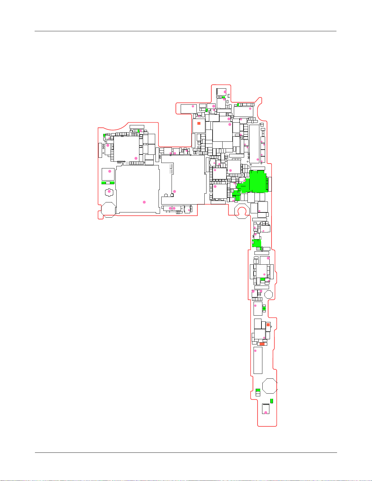
PCB Diagrams
8-2.
8-2-1.
Top
8-2
Confidential and proprietary-the contents in this service guide subject to change without prior notice.
Distribution, transmission, or infringement of any content or data from this document without Samsung’swritten authorization is strictly prohibited.
 Loading...