

Samsung SM-R765A, Gear S3 Frontier 4G LTE Schematics TSHOO
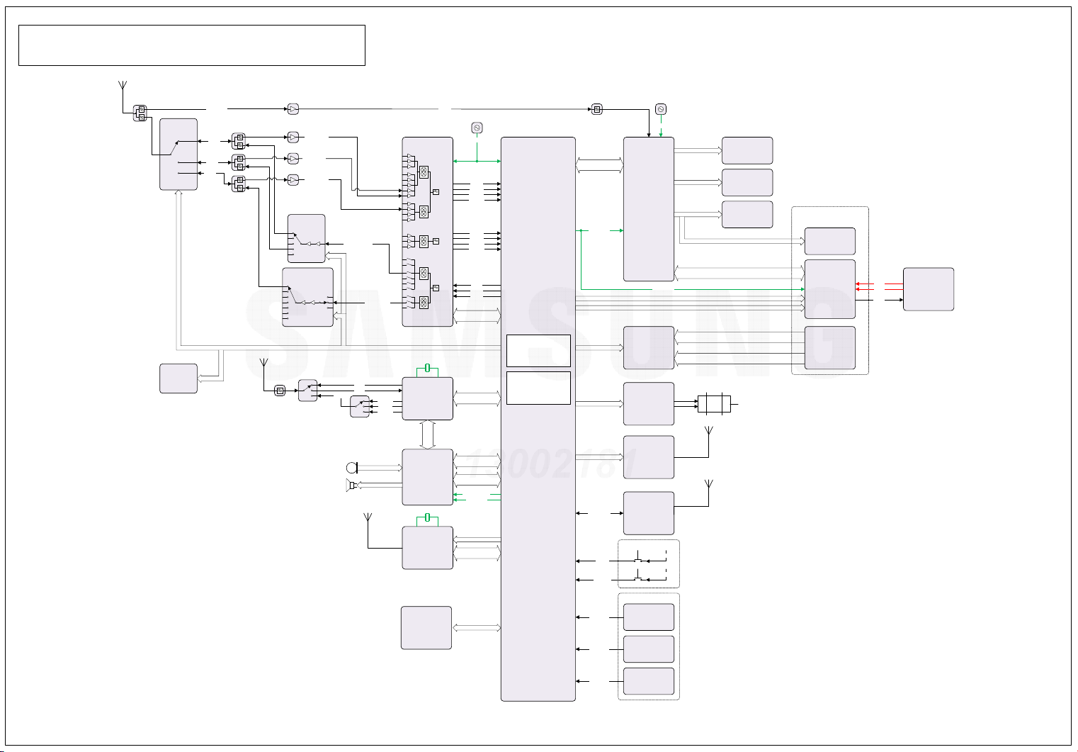
SOLIS SIGNAL BLOCK DIAGRAM
(VIETMOBILE.VN)
SP4T
BGSA14GN10-1
DC-DC
SKY87006
GPS_ANT_IN
TRX_B2
TRX_B4
TRX_B5
PRX_TR_IN_B2
PRX_TR_IN_B4
PRX_TR_IN_B5
MMMB
SKY77652
MMMB
SKY77651
RFFE0
BT_TX
SPEAKER
TX_TR_OUT_B2_4
2G_TX
2G_RX
MIC
TX_TR_OUT_B5
BT_TX_14
BT_TX_4
BT_TX_20
MAIN_MIC
SPK_OUT
TRANCEIVER
S5M910DX01
HB
MB
LB
HB
MB
LB
37.4MHz
BT/WLAN
BCM43012B0
BT_PCM
CODEC
WM1831
27.12MHz
NFC
PN67T
Factory POGO
GSP_RF
MAIN_TCXO_26M_IN
PRX_I_P
PRX_I_N
PRX_Q_P
PRX_Q_N
DRX_I_P
DRX_I_N
DRX_Q_P
DRX_Q_N
TX_I_N
TX_Q_P
TX_Q_N
XCP_RFIC0_SPI
WLAN_SDIO
MM_I2S
CODEC_SPI
CDEOC_26M_AP
32KHZ_PMIC
NFC_I2C
ESE_SPI
USB_DP/DM
AP+CP+PMIC
Exynos7270
(JAVA-W)
ePOP Memory
6Gb LPDDR3
32Gb eMMC
PMIC
S2MPW01
SHUB_SPI
32KHZ_PMIC
TPS_I2C
MOT_I2C
WPC_I2C
MST_DATA_A
ON_SW
BACK_KEY
HALL_INT_1
HALL_INT_2
26MHz
SENSOR HUB
+ GPS
BCM4774
32KHZ_PMIC
TSP
TMA525A
MOTOR DRIVER
ZH915
WIRLESS
CHARGER
P9220S-0AHGI8
MST
ISP7022
KEY FPCB
VREG_L3_1P8
HALL IC FPCB
HALL SENSOR
S-5712CCDL1
HALL SENSOR
S-5712CCDL1
V_BATT
BARO_I2C
HRM_I2C
SENSOR_I2C
DISP_MIPI_D0
DISP_MIPI_CLK
MOTOR
BAROMETER
LPS22HB
HRM SENSOR
PPSD400
6-Axis SENSOR
LSM6DSL
OPR_SDIO
X[0:7]
Y[0:7]
1.3"
DISPLAY MODULE
ILLUMINATION
SENSOR
TSL2584TSV
DDI
TOUCH
PANEL
TX_I_P
TX_I_P
EL_ON
DC-DC
STOD32WB
HALL_INT_3
HALL SENSOR
S-5712CCDL1
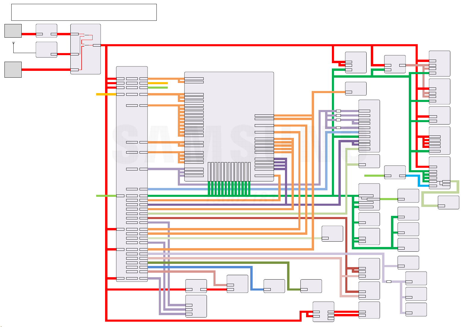
SOLIS POWER BLOCK DIAGRAM
Factory
POGO
V_BUS_5V_IF
OVP
KTS1681
IN OUT V_BUS_5V
CHGIN
PMIC
S2MPW01
(VIETMOBILE.VN)
BATTERY
380mAh
WIRELESS
CHARGER
P9220S-0AHGI8
V_BATTERY
VSYS
VDD_WLCHG
OUT
WCIN
VBATT
V_BATT VDD_BUCK1_0P8
VDD_BUCK3_1P35
VDD_BUCK4_2P0
V_BATT
V_BATT
PMIC
S2MPW01
VINB1 BUCK1/2 SW1
VINB3 BUCK3 SW3
VINB4 BUCK4 SW4
VINL3 LDO1
LDO2
LDO7
LDO22
LDO4
LDO5
VINL4 LDO3
LDO8
LDO10
LDO15
LDO21 VLDO21 VREG_L21_1P8
LDO17
LDO13
VINL1 LDO6
LDO9
LDO11
LDO12
VINL2
LDO23
LDO14
LDO16
LDO18
LDO19
LDO20
VINB BOOST SWBV_BATT VDD_HRM_5P0
VLDO1
VLDO2
VLDO7
VLDO22
VLDO4
VLDO5
VLDO3
VLDO8
VLDO10
VLDO15
VLDO17
VLDO13
VLDO6
VLDO9
VLDO11
VLDO12
VLDO23
VLDO14
VLDO16
VLDO18
VLDO19
VLDO20
VDD_BUCK3_1P35
VDD_BUCK4_2P0
VREG_L1_0P8
VREG_L2_0P9
VREG_L7_1P2
VREG_L22_1P2
VREG_L4_1P2
VREG_L5_1P0
VREG_L3_1P8
VREG_L8_1P8
VREG_L10_1P8
VREG_L15_1P8
VREG_L17_1P8
VREG_L13_1P8
VREG_L6_3P0
VREG_L9_3P0
VREG_L11_3P0
VREG_L12_3P3
VREG_L23_1P8
VREG_L14_2P8
VREG_L16_3P3
VREG_L18_3P0
VREG_L19_2P8
VREG_L20_3P0
VDD_CORE
VDD_CP
VDD_CORE_M
VDD_CP_M
VDD09_ALIVE
AVDD09_USB20
AVDD09_MIPI_DPHY
AVDD09_DAC0_CP
AVDD09_WLBT_WPLL
VDD09_PLL_CPU
VDD09D_PLL_MIPI
VDD09_PLL_AUD
VDD09D_PLL_AUD
VDD09_PLL_SHARED
AVDD09_MPLL_CP
VDD2_MEM
VDDQ12_DRAM0_CKE
AVDD_12_MIPI_DPHY
VDDQ_MEM
VDDQ12_DRAM0
VDDQ12_DRAM0_CLK
AVDD12_ADC0_CP
AVDD12_WLBT_WPLL
AVDD12_MPLL_CP
LOAD SWITCH
FPF2495BUCX
V_BATT
VIN VOUT VBAT_MST
PPSD400
IO_SUP
VREG_L13_1P8
RX_SUP
VREG_L12_3P3
TX_SUP
VDD_HRM_5P0
HRM
V_BATT
AP+CP
Exynos7270
VDD18_RTC
AVDD18_ADC
AVDD18_TCXO
VDDQ18_ALIVE
VREG_L20_3P0
VDDQ18_AUD
VDDQ18_EXT0
VDDQ18_RFIO_CP
VDDP18_USIM01_CP
AVDD18_VCTCXO_CP
MST
ISP7022
VCC
VM
V_BATT
V_BATT
VREG_L3_1P8
V_BATT
VREG_L3_1P8
V_BATT
VREG_L3_1P8
V_BATT
VREG_L3_1P8
V_BATT
VREG_L3_1P8
VBATT
VCC1
VCC2
VIO
VBATT
VCC1
VCC2
VIO
VBAT
VDD_PAD
TX_VDD_V5P0
VDD_V5P0
SR_VDDBAT5
LDO_VDDBAT5
VDD_1P8
SPKVDD
CPVDD
AVDD
DBVDD
MICVDD
DCVDD
VDD_MICBIAS_1P8
MMMB PAM
SKY77912-21
MMMB PAM
SKY77651-21
NFC
PN67T
BT/WLAN
BCM43012B0
CODEC
WM1831
SD18OB216-018
VCC
MICBIAS1
MICBIAS2
MIC
FEM
SKY77912-21
V_BATT
VBATT
VCC
VIO
eSIM
O1090845
VCCVREG_L23_1P8
BEAD
SENSOR
TSL2584TSV
VO2
VO3
VDD_RF_RXLO_1P2
BEAD
VDD_RF_TXLO_1P2
BEAD
VDD_RF_RX_1P2
BEAD
VDD_RF_TX_1P2
VREG_L10_1P8
VREG_L21_1P2
VREG_L17_1P8
VREG_L16_3P3
VDD_UB_ELVSS_-4P0
VREG_L5_1P0
VREG_L3_1P8
VREG_L4_1P2
VCC_MEM
AVDD33_USB20
AVDD18_USB20
AVDD18_PLL_CPU
AVDD18_PLL_AUD
AVDD18_ADC0_CP
AVDD18_DAC0_CP
AVDD18_MPLL_CP
VCCQ_MEM
VREG_L23_1P8
VREG_L9_3P0
VREG_L6_3P0
VREG_L15_1P8
VREG_L10_1P8
VDDQ1830_USIM0_CP
VDDQ1830_USIM1_CP
AVDD18_MIPI_DPHY
AVDD18_PLL_SHARED
AVDD18_WLBT_WPLL
VDD1_MEM
VDDP18_MMCCARD
VDDQ18_MMCEMBD
VDDQ1833_MMCCARD
ILLUMINATION
VDD
GPS LNA
BGU8309
VCC VREG_L18_3P0
MOTOR DRIVER
DRV2624
VDDVREG_L13_1P8
DC-DC
STOD32WB
VINA VO1
V_BATT VDD_UB_ELVDD_4P6
VINP
VREG_L3_1P8
TRANCEIVER
S5M910DX01-
L030
VDD12_RXLO
VDD12_TXLO
VDD12_PRX
VDD12_DRX
VDD12_TX
DVDD10
DVDD18
VDD18_RX
VDD18_TX
VDD18_TXLO
TCXO
KT1612A26000
VDDVREG_L21_1P2
VDD_BUCK4_2P0 VDD_CODEC_1P2
SENSOR HUB
+ GPS
BCM4774
VDD_PMU_IN
VDD1P8_AUX VDD18_TCXO_HUB
VDD_PMU_IN_AON
VDD_IO
6-Axis SENSOR
LSM6DSL
VDD
BAROMETER
LPS22HB
VDD
VDD_IO
TSP
TMA525A
VCCD
VDDD
VDDA
1.3" UB DDI
VDD3
VCI
1.3" UB PANEL
ELVDD
ELVSS
V_BATT
DC-DC
SKY87006
IN OUT
VIOVREG_L3_1P8
LDO
RP103K121D-TR
VDD VOUT
VDD
VDD
VDD
VDDVREG_L3_1P8
BGSA14GN10-1
VDDVREG_L14_2P8
BEAD
VDD_LNA_2P8
TCXO
KT1612A26000
HALL SENSOR
S-5712CCDL1
HALL SENSOR
S-5712CCDL1
HALL SENSOR
S-5712CCDL1
ANT SWITCH
SFMLB2RB002
VDD
SFMLB2RB002
VDD
SFMLB2RB002
VDD
VPA_APT1
RF LNA
RF LNA
RF LNA

SPK401
SPK400
ANT100
MOT500
L159
C101
V101
L168
SUS102
C106
ANT104
MOT501
L103
TP424
TP423
TP422
TP421
CN402 CN403 CN404 CN405
L500
L503
TP608
TP606
TP609
TP425
TP602
TP603 TP604TP605
TP426
TP610
TP607
L404
L405
BOTHHOLE101
ZD400
ZD401
ANT101
ZD407
ZD408
C544
BAT400
BAT401
C169
V300
C367
R312
U503
U101
L112
L111
C121
TP601
C522
L605
L606
C638
(VIETMOBILE.VN)
TP223
TP401
TP403
TP400
OSC500
TP402
ANT600
L611
BOTHHOLE100
TP409
TP405
TP404
TP407
TP406
TP100 TP101
R416
C122
C123
C120
C162
C163
L109
C109
TP229
TP230
TP228
TP410
JTAG306
C543
SUS101
R342
R344
TP_UB
R339
C620
C617
L600
C605 C606
L609
C610
C615
C618
C621
C637
L604
L608
L603
F600
C614
C635
C607
C627
C644
U603
U601
C641
C368
R313
C632 C633
V301
OSC600
TP416
R357
TP600
R358
TP300
C438
C437
TP301
TP419TP420
TP417 TP418
OSC400
R305
R301
C348
C359
C339
C332
C362
C319
C363
C316
C357
C318
C355
C317
C354
C410 C411
C356
C323
R302
C320
C358
C458
C364
C442
C351
C412
C344
R404
MIC400
ZD404
POGO404
C626
C628
C307
C346
C313
C337
C315
C331
C333
R300
C300
C365
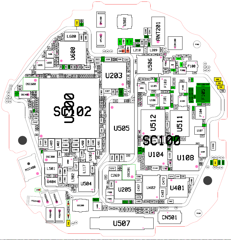
SC102
U300
C407
C444
L403
L402
C366
L300
R315
C441
OSC300
L505
L501
C485
L504
C503 C504
U404
C477
POGO401
POGO400
POGO402
POGO403
L601
C624
C301
C309
C403
C406
C488
C439
C500C501
C513
U600
L602
C622
C608
C306
C336
C352
C400
C416
C402
C418
C414
C401
C413
C424
C433
C420
U500
C127
C415
L502
C514
R516
C516
C517
R332
R331
TP520
R506
R507
ZD405
R409
R406
ZD406
TP518
R418
L610
C310
C124
U504
SOC200
TP519
C602
C616
C325
L400
C408
R341
C611
C328
C417
L117
R412
C601
C619
C338
C604
C603
C609
C600
C305
C311
C404
C487
U103
C330
C405
C128
C515
C613
C612
TP302
C254
C350
C308
L401
C419
C126
C428
R417
U405
WPC400WPC401
TP220
TP222
C491
C239
C489
C490
R413
C455
C456
C255
C252
C251
U203
R205
C345
C327
C303
C312
C314
C329
C347
C324
C349
C335
C321
C322
R306
C334
C432
C342
C426
C343
C431
C340
C421
C341
C353
C434
R307
C422 C423
C425
C427
C245
R214
C482
F500
F501
R419
R420
C467
C468
TP221
ZD403
R329
C545
C519
R330
C302
C326
C304
C535
U505
C409
C486
C534
C266
C272
C267
C269
C246
U205
R351R352
R309
U507
U502
C243
R213
C459
C460
C463
C248
C242
R209
ZD402
C244
TP231
R510
R337
OSC201
R323
R326
C361
C532
C524
C249
C253
R204
R511
R403
TP224
C523
C525
R319
C520
R318
C235
U501
TP225
C511
R349
R350
TP501
R113
L139
TP513
C533
R338
L142
L140
V100
C156
R103
L133
C148
C149
SC100
L158
L156
L157
L148
L149
C270
C174
L125
L124
C132
L128
L129
C139
C466
C471
C457
R402
R410
C470
C452
C465
R325
R321
R322
R324
C506
C510
C502
C505
C360
R308
R310
R311
C509
R501
C240
C241
C238
ANT201
R212
C236
R206
TP226
L209L210
TP227
C528
C530
C527
U506
C531
C546
U105
C166
U106
C165
U512
C131
L121
C135
C146
C147
C151
U104
C143
C144
C142
L134
U402
C451
C453
C537
C539
C507
C536
C538
C508
L507
C237
TP527
L511
C526
C529
F502
L508
L137
L138
F103
L135L136
F101
C133 C134
L123
L131
C150
C145
L132
C473
C483
C454
R316
R317
R411
TP415
CN501
CON100
TP505
TP503
C227
U202
L208
C229
C540
C137
C140C141
L127
L120
C129 C130
C117
C104
C194
C196
U511
R105
R104
R106
C108
C157
C159
C161
C155
C160
C154
C153
C152
U108
L130
C107
C158
C474
U401
C462
TP427TP428
TP102
C100
C102
L102
L160
C112
L203
C232
L211
C271
F100
L207
F200
C228
C138
R112
L126
F102
C105
L101
U102
C164
L143
L110
C110
C111
L106
C118
C448
C447
TP516
TP511
TP515
TP506
TP512
L100
L155
F105
L145
L146
L147
C175
C198
U109
R114
C197
R327
R328
R353
R354
R355
R356
C446
TP500
TP502
TP504
TP514
R345
R346
R347
R348
TP508
TP509
TP507
TP510
L105
C103
C177 C178
L154
C176
L152
L161
L150 L151
C180
L153
C172 C173
L141
C170C171
L144
F104
U107
R111
C450
C461
C449
TP408
TP103
8. Level 3 Repair
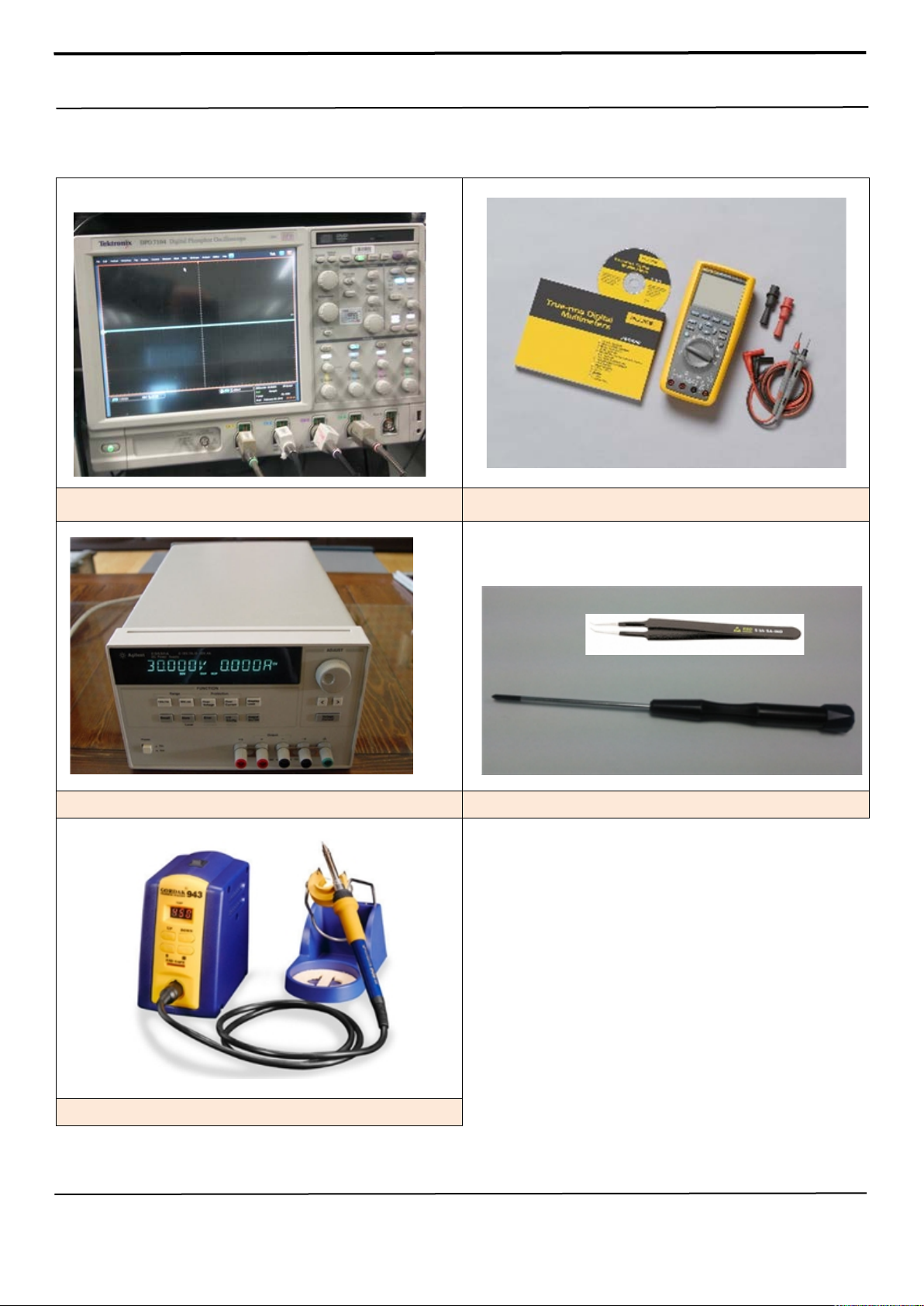
Power Supply
Y/+ driver, ESD Safe Tweezer
Soldering iron
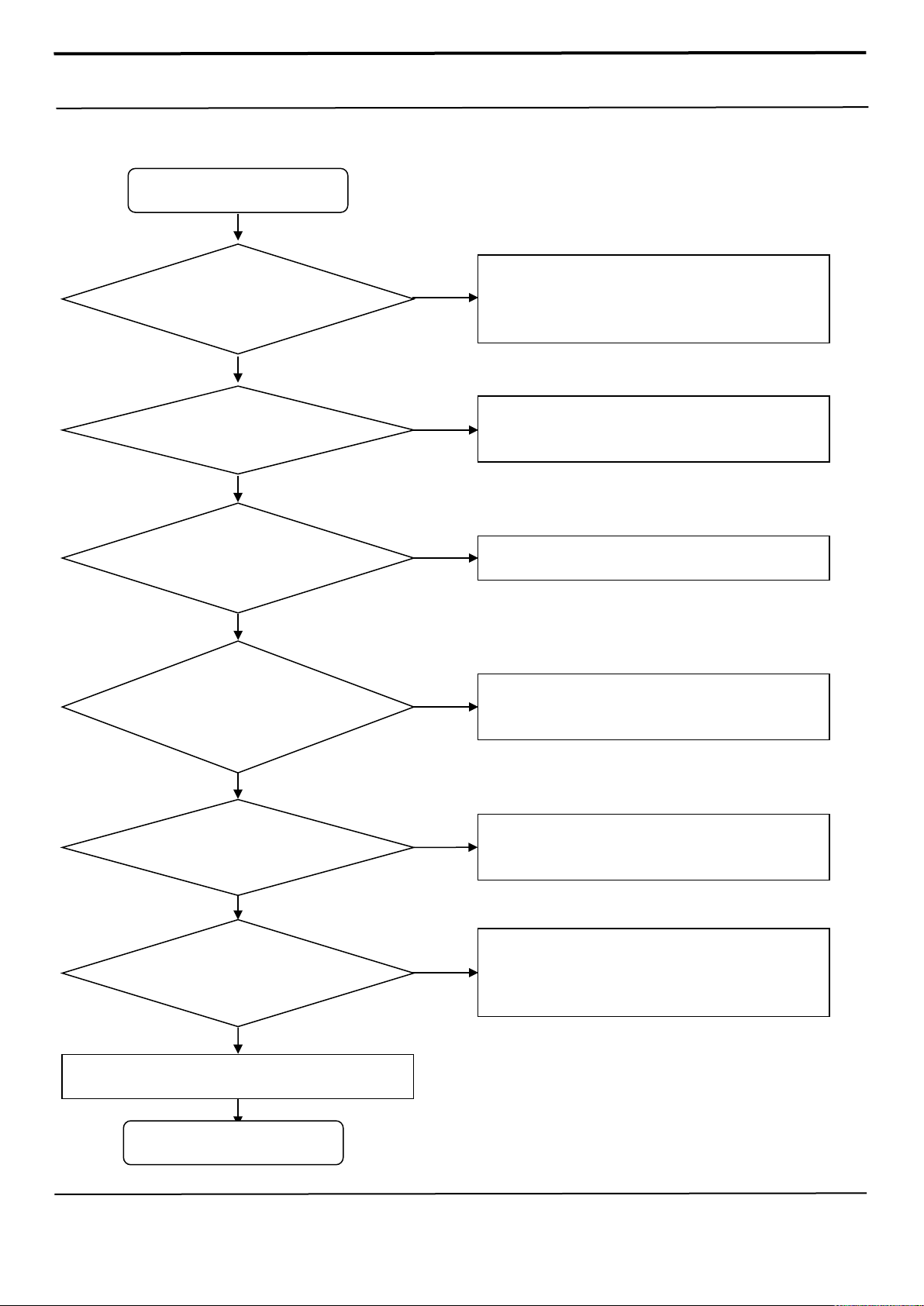
8-3. Flow chart of Trouble shooting.
Oscilloscope
Digital Multimeter
Confidential and pr oprietary-the c ontents in this ser vice guide subject to change wi thout prior noti ce
Distribution, transmi ssion, or infringement of any content or data from this document without Samsung’s written authorization is strictly prohibited.
8. Level 3 Repair
Yes
Yes
Yes
No
Abnormal
No
No
Yes
No
Yes
No
Check the Internal Battery
Is it more than 3.4V?
Check the key-FPCB
(open, etc)
Power-on the Watch and
Sound or vibration is ok?
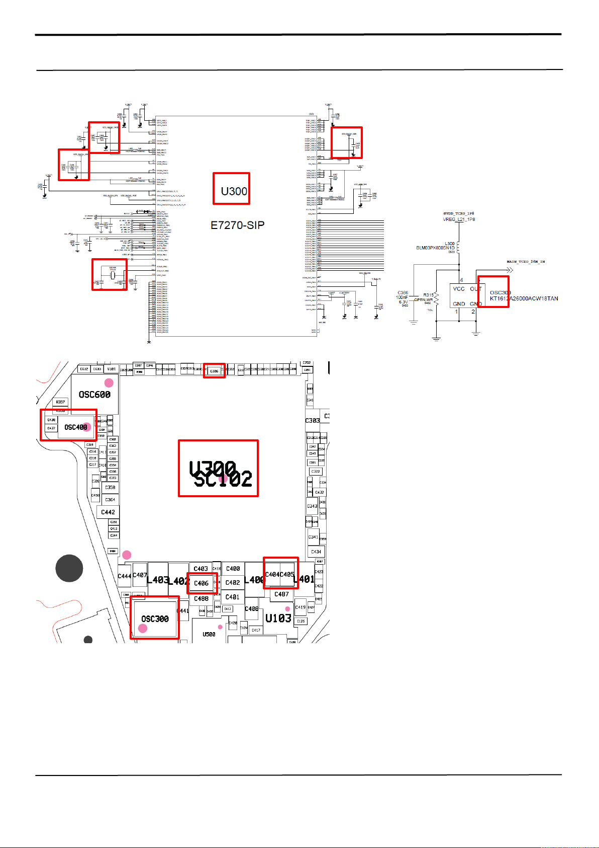
Check the U300 output
Check the OSC400 output
(C437,C438)
Check the
8-4-1. Power On
Watch does not power on.
check the power-on sound
(C405 = 0.8V, C404 =
Clock OSC300(C306)
check the initial operation
Voltage.
voltage
clock
END
Charging the battery by TA.
If its voltage level is extremely low(under 3.0V),
Change the battery.
Change the key-FPCB
And retry to the power-on operation.
Yes
Change the OCTA LCD ASSY
Replace the U300
Replace the C306 or OSC300
Replace the OSC400.
※ Test condition (Oscilloscope setting)
: 20.0us.div (time division)
Confidential and pr oprietary-the c ontents in this ser vice guide subject to change wi thout prior noti ce
Distribution, transmi ssion, or infringement of any content or data from this document without Samsung’s written authorization is strictly prohibited.
8. Level 3 Repair
Confidential and pr oprietary-the c ontents in this ser vice guide subject to change wi thout prior noti ce
Distribution, transmi ssion, or infringement of any content or data from this document without Samsung’s written authorization is strictly prohibited.
8. Level 3 Repair
Yes
Abnormal
No
Normal
Abnormal
Re-download the latest
S/W on the Watch.
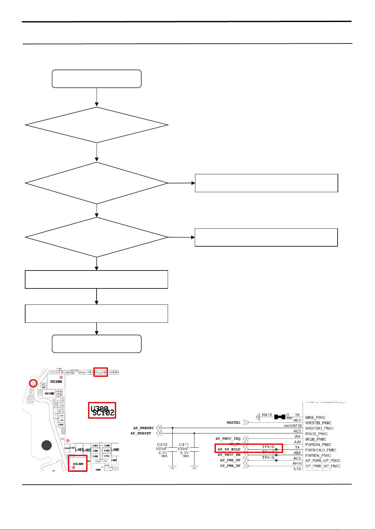
Check the
Check the
Is that frequency 26Mhz?
Yes
Abnormal
8-4-2. Initial (Lock up)
Initial (Lock up)
PMIC_PS_HOLD
Clock OSC300(C306)
Replace the U300
Replace the PBA
END
Replace the U300 (Crack, Open, etc.)
Replace the C306 or OSC300
Confidential and pr oprietary-the c ontents in this ser vice guide subject to change wi thout prior noti ce
Distribution, transmi ssion, or infringement of any content or data from this document without Samsung’s written authorization is strictly prohibited.
8. Level 3 Repair
No
Yes
Yes
Charging Sequence Start
Yes
Yes
8-4-3. Charging Part
Insert Charging Dock
TA / USB Insert
Check the lighting LED
indicator on the Cradle
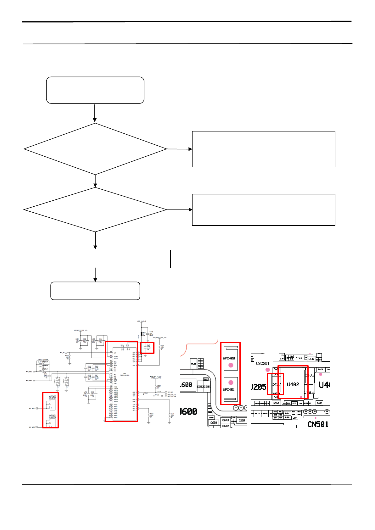
Check the voltage on the
C457=4.6V
Replace the U300
END
Check may not connected TA or
Replace the Cradle or
Check the WPC RX coil
No
Check SMD condition of WPC400, WPC401, C459, C465,
C466, C470, C471.
If they are alright, replace the U402
Confidential and pr oprietary-the c ontents in this ser vice guide subject to change wi thout prior noti ce
Distribution, transmi ssion, or infringement of any content or data from this document without Samsung’s written authorization is strictly prohibited.
 Loading...