

Samsung Galaxy S4, GT-I9295 Troubleshooting
Level
8.
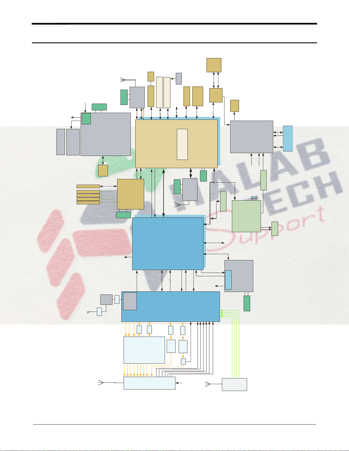
Block Diagram
8-1.
P
A
k
c
u
b
Repair
3
z
H
1
9
M
s
k
c
u
b
2
s
o
r
r
o
x
I
T
C
R
E
T
s
M
M
A
3
1
C
D
E
L
C
.
M
r
D
I
5
z
F
3
le
I
H
3
C
S
z
H
X-TAL
M
9
32768Hz
1
r
e
K
f
f
L
u
C
B
s
k
c
u
b
8
D
E
L
R
I
B
e
n
G
S
R
I
T
N
e
s
t
G
u
r
e
/
p
E
E
x
ic
I
T
N
N
G
A
M
I
T
N
M
O
R
A
B
I
T
N
6
A
I
T
N
W
A
S
T
N
A
N
I
A
M
O
r
e
f
t
f
e
u
s
s
b
e
O
r
O
I
l
k
D
c
P
a
L
u
lo
G
6
n
c
3
a
C
M
T
R
I
,
2
C
I
,
2
C
C
I
,
2
I
,
2
C
I
,
2
C
z
6
8
H
L
A
T
L
E
S
_
W
S
_
T
N
A
A
W
A
N
S
L
)
0
2
/
)
8
8
/
/
7
5
/
/
5
2
d
/
/
a
3
1
/
u
B
1
(
Q
B
d
(
:
a
a
t
u
G
n
2
Q
e
:
P
:
G
3
E
T
L
x
T
M
S
G
u
M
4
d
W
4
/
.
o
M
7
T
C
m
3
B
B
O
I
T
D
R
S
A
_
U
N
_
A
T
L
B
W
C
2
T
I
N
I
R
U
b
U
-
u
R
H
A
H
r
5
o
L
8
s
2
n
1
e
C
U
S
T
A
3
2
7
-
X
Q
I
S
P
G
S
P
G
)
/2
)
1
8
/
B
B
B
L
M
S
G
5
(
B
H
(
B
W
B
H
M
A
L
S
G
S
G
3
G
3
8
/
5
/
D
4
N
/
3
A
/
B
2
/
1
x
T
x
x
x
x
x
S
T
T
T
T
T
C
5
3
1
2
8
P
B
B
B
B
B
D
M
D
e
E
L
G
e
6
ic
1
v
r
e
S
M
C
C
P
8
2
I
_
T
B
T
T
S
IN
R
C
I
S
H
2
3
B
W
E
A
T
S
L
D
A
A
P
8
U
8
3
B
Q
7
F
M
R
M
M
S
M
G
x
x
T
T
0
2
7
B
B
H
)
H
a
T
t
C
id
A
n
T
M
I
e
P
E
P
W
F
(
F
S
R
C
D
C
D
D
C
L
e
n
la
4
I
P
I
M
r
o
s
s
e
c
o
r
P
ll
a
C
3
I
B
S
S
R
E
V
I
E
C
S
N
A
R
T
M
A
P
M
A
C
T
V
e
n
la
C
2
4
2
I
I
P
I
M
3
R
4
6
D
0
D
8
P
Q
L
P
B
A
G
2
C
2
I
)
4
z
L
9
H
A
7
T
M
C
0
-
7
X
2
F
2
N
M
C
B
(
M
5
1
2
9
M
D
M
IQ
X
N
R
O
Q
D
I
F
/
X
R
/
T
IQ
A
X
X
T
R
R
A
P
D
P
G
L
5
0
6
1
R
T
W
W
A
S
E
T
L
x
R
W
A
7
B
S
E
T
L
0
7
2
D
M
E
D
N
T
A
N
L
A
P
A
B
B
x
X
T
P
7
D
B
L
E
S
_
W
S
_
T
N
A
e
n
la
I
P
4
I
S
P
I
M
0
4
L
H
M
e
n
la
4
I
M
D
H
x
x
R
R
3
1
B
/B
2
B
P
2
S
I
8
I
I
S
e
n
la
4
I
C
P
2
I
I
M
z
L
H
A
T
M
-
7
X
2
S
U
B
M
I
L
S
I
S
M
I
F
I
B
S
S
N
0
_
E
D
L
_
_
C
1
K
9
.
M
2
M
z
I
P
A
M
P
C
X
x
X
x
R
R
R
R
S
8
0
5
C
2
B
B
/
P
B
/
/
0
M
S
5
S
C
8
G
D
M
E
S
G
T
N
A
y
it
s
r
e
iv
D
h
s
la
t
F
e
S
h
s
la
F
3
0
8
7
7
X
A
M
Detect
EAR Rx/Tx
S
U
B
M
I
L
S
S
N
ic
m
2
C
I
8
D
M
H
1
M
9
s
1
k
M
c
0
u
8
P
r
b
M
e
f
P
6
f
P
u
C
B
X
x
X
R
R
x
R
D
D
R
D
3
0
/
D
/8
2
1
7
5
B
B
B
B
H
H
)
T
C
b
M
A
T
u
I
E
P
s
F
W
(
F
S
R
r
r
O
e
h
e
e
g
r
P
a
V
h
c
O
W
S
P
/
D
M
X
_
R
/
D
T
_
B
P
S
C
U
0
1
3
9
D
C
W
r
e
s
f
f
O
u
D
b
L
K
4
L
1
C
z
H
O
M
X
2
C
.
T
9
1
g
G
D
s
iv
u
L
T
r
la
C
a
t
I
d
O
F
u
G
M
r
B
o
l
M
o
U
t
e
e
S
f
A
o
u
U
a
C
F
M
S
D
+
L
X
/
D
/
-
R
R
/
D
T
S
P
P
P
V
A
A
P
P
A
C
h
c
it
w
s
1
2
ic
ic
M
M
V
C
R
s
C
D
A
V
e
5
c
r
a
f
o
r
t
e
c
t
e
M
in
n
D
_
n
in
C
o
I
p
c
U
1
M
1
IO
K
P
P
D
M
S
U
A
A
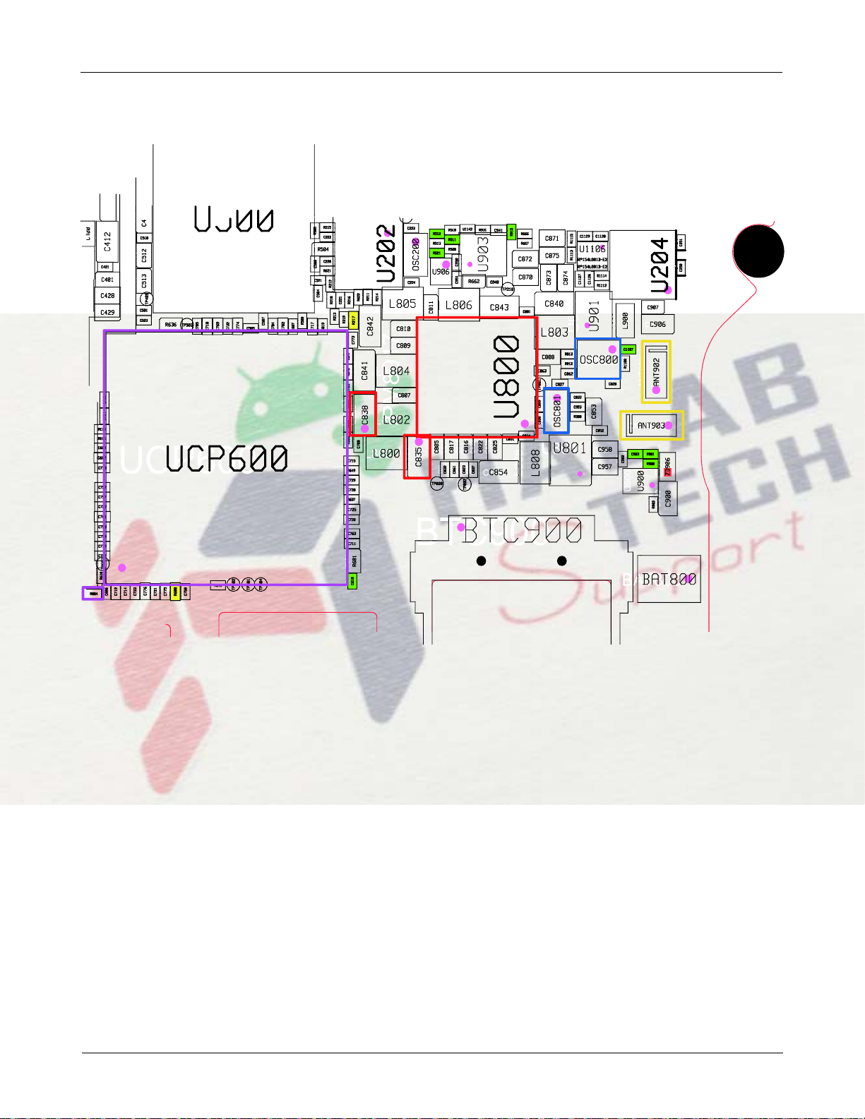
8-1
Confidential and proprietary-the contents in this service guide subject to change without prior notice.
Distribution, transmission, or infringement of any content or data from this document without Samsung’swritten authorization is strictly prohibited.
Level3Repair
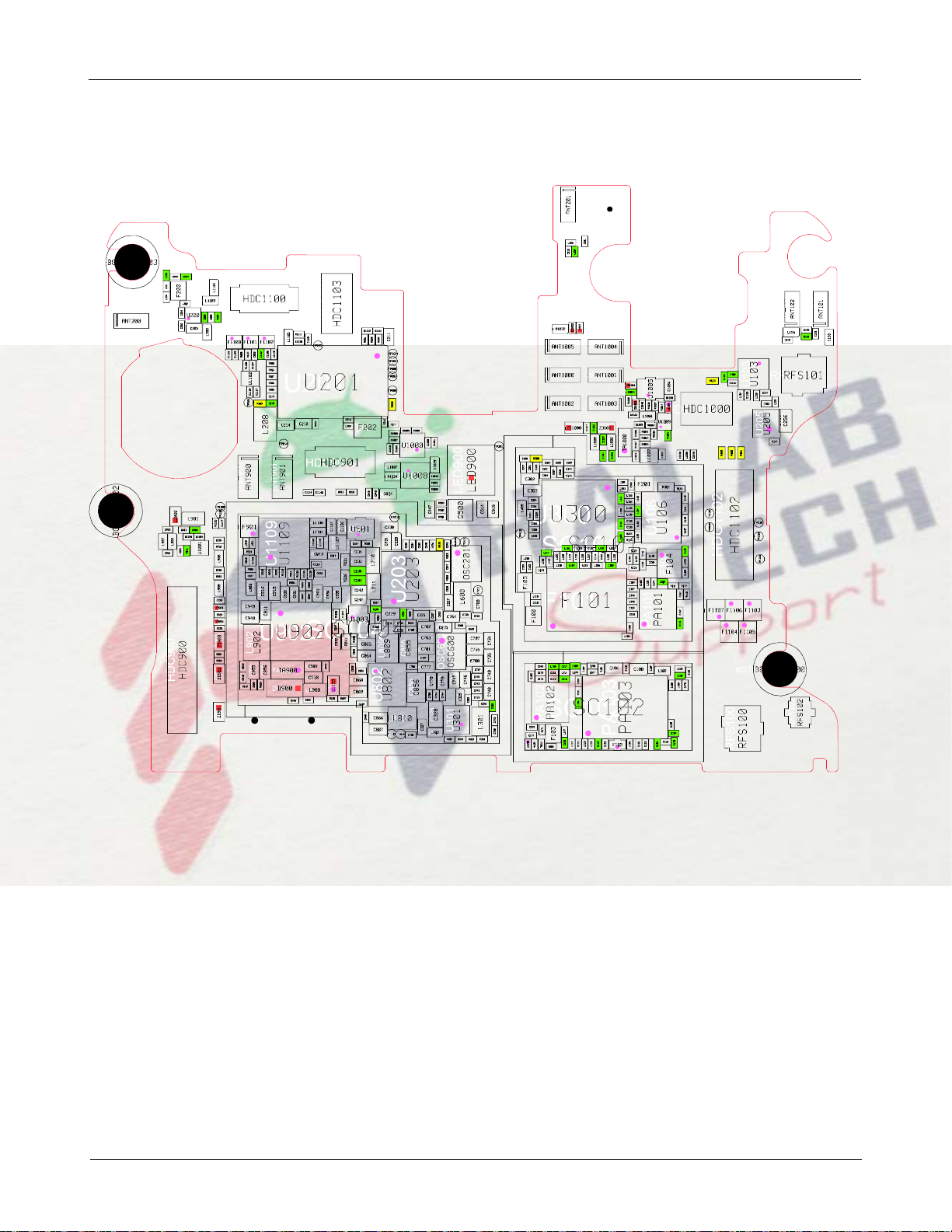
PCB Diagrams
8-2.
8-2-1.
Main PCB Top
8-2
Confidential and proprietary-the contents in this service guide subject to change without prior notice.
Distribution, transmission, or infringement of any content or data from this document without Samsung’swritten authorization is strictly prohibited.

Level3Repair
8-2-2.
Bottom
8-3
Confidential and proprietary-the contents in this service guide subject to change without prior notice.
Distribution, transmission, or infringement of any content or data from this document without Samsung’swritten authorization is strictly prohibited.
Level3Repair
8-2-3.
Sub PCB Top
8-4
Confidential and proprietary-the contents in this service guide subject to change without prior notice.
Distribution, transmission, or infringement of any content or data from this document without Samsung’swritten authorization is strictly prohibited.
Level3Repair
8-2-4.
Sub PCB Bottom
8-5
Confidential and proprietary-the contents in this service guide subject to change without prior notice.
Distribution, transmission, or infringement of any content or data from this document without Samsung’swritten authorization is strictly prohibited.

Level3Repair
Flow Chart of Troubleshooting
8-3.
Equipments
Oscilloscope
Power Supply
á
Digital Multimeter
á
driver, ESD Safe Tweezer
á+
8960 &
Confidential and proprietary-the contents in this service guide subject to change without prior notice.
Distribution, transmission, or infringement of any content or data from this document without Samsung’swritten authorization is strictly prohibited.
Spectrum Analyzer
8-6
Soldering iron
á
Level3Repair
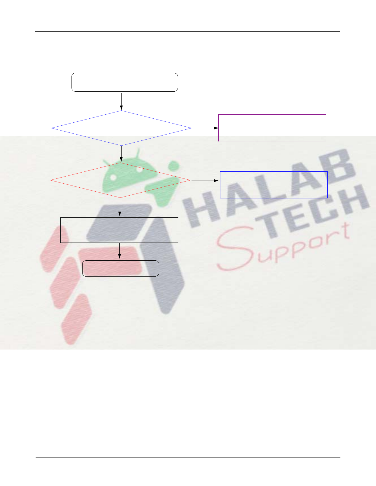
8-3-1.
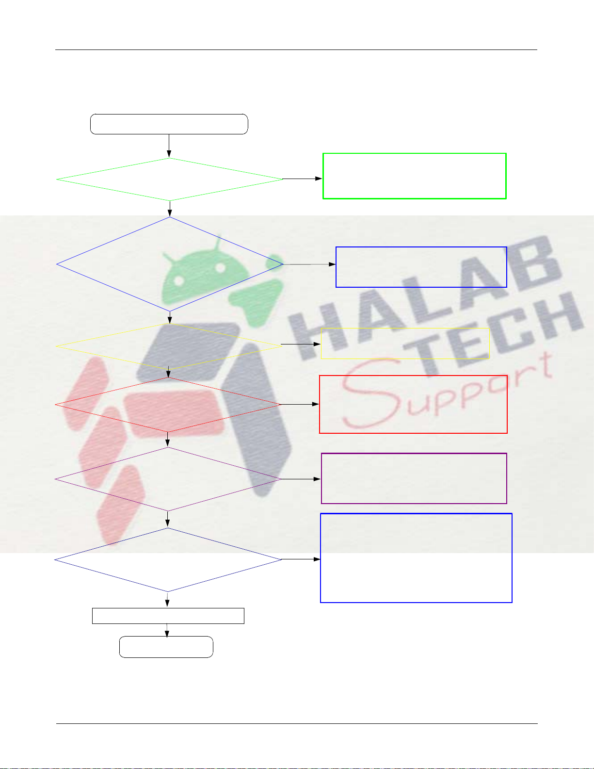
Power On
Cell-phone can`t power on.
Check the Battery Voltage
Battery >
Power-on the phone and check
the power-on sound
or motor vibration.
Sound or vibration ok
Check the ANT902/ANT903
Are power-key clips damaged
Yes
No
3.4
V?
.
?
?
No
Yes
Abnormal
Connect TA to charge the battery.
Change the LCD ASSY
Change thepower-key clips.
And retry to the power-on operation.
Yes
Check the U800 output voltage
C835=1.225V, C838=1.05V)
(
Yes
Check the U800 output signal
PM8917_PS_HOLD(R804)
(
Check the OSC801
Is it around32KHz?
check the initial operation
1.8
END
V)
Yes
Yes
Yes
No
=
No
No
If the output voltage is not satisfied with normal
condition, replace U800.
If the output voltage is not satisfied with normal.
condition, replace UCP600
Change the OSC801
If OSC800 still does not work, replace U800
Test condition(Oscilloscope setting)
※
us.div(time division)
:20.0
8-7
Confidential and proprietary-the contents in this service guide subject to change without prior notice.
Distribution, transmission, or infringement of any content or data from this document without Samsung’swritten authorization is strictly prohibited.
Level3Repair
8-8
Confidential and proprietary-the contents in this service guide subject to change without prior notice.
Distribution, transmission, or infringement of any content or data from this document without Samsung’swritten authorization is strictly prohibited.
Level3Repair
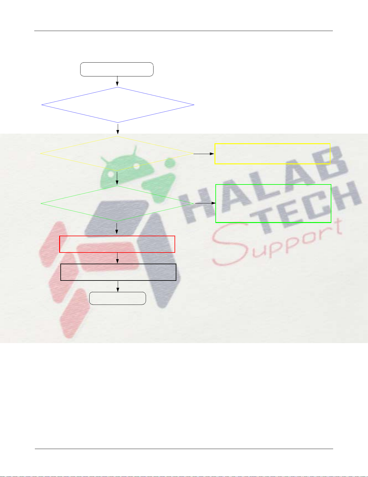
8-3-2.
Initial
Initial Failure
Yes
Re-download Software
Abnormal
Check the AP Reset
PM8917_PON_RESET_N(C933)
Check the oscillator clock
V(High)
1.8
waveforms.
Mhz:OSC800
19.2
Yes
Normal
=
No
Abnormal
Check the U800
Check the OSC800
Check the output clock waveforms and frequency.
Test condition(Oscilloscope setting)
※
us.div(time division)
:20.0
Change UCP600
Abnormal
Change PBA
END
8-9
Confidential and proprietary-the contents in this service guide subject to change without prior notice.
Distribution, transmission, or infringement of any content or data from this document without Samsung’swritten authorization is strictly prohibited.
Level3Repair
1
0
2
7
C225
C229
2
3
2
2
3
7
C323323C32432
4
3
2
5
2
5
C3263626
3
2
7
2
7
2
8
3
2
9
3
2
9
3
3
0
3
3
0
0
6
0
5
6088C60960
9
C700
C701
C702
C703
C706706
6
C707707
7
C709709
9
C713713
3
C737300C73373
7
3
4
3
4
7
3
5
3
5
C736
C737
C738
7
3
9
7
3
9
9
C740
7
C741
7
7
4
2
7
4
2
7
4
4
7
4
4
4
C745
7
7
4
6
4
6
7
4
7
4
4
7
7
4
8
4
8
7
4
9
4
9
7
5
4
7
5
5
4
C75755
5
C75756
6
7
5
8
7
5
5
8
C760
7
C764
C777
7
7
8
7
8
7
7
9
7
9
C815
4
8
C884
5
0
8
5
5
5
6
C8585
7
C864
C867
C868
C909
9
1
2
9
1
8
9
1
9
9
2
2
2
2
9
3
2
2
9
3
3
3
3
C93693
6
C93793
7
C948
9
5
5
5
9
5
6
6
3
0
1
0
L302
8
0
9
9
9
0
2
2
L908
S
C
6
0
0
0
1
0
0
2
1
0
0
5
R
2
2
0
2
2
5
2
2
5
R30233002
R30333003
R62566225
R627662272766228
9
0
9
9
9
1
0
9
1
1
R9129191
2
TA900
TP_SSBI_CLK
S
IIC
C
L
CLCL
L
TP803TP
3
1
1
3
3
3
3
0
1
3
0
1
3
0
1
M
3
2
6
2
T
M
X
3
3
M
222
6
T
M
T
T
X
8
0
2
2
8
8
0
2
8-10
Confidential and proprietary-the contents in this service guide subject to change without prior notice.
Distribution, transmission, or infringement of any content or data from this document without Samsung’swritten authorization is strictly prohibited.
Level3Repair
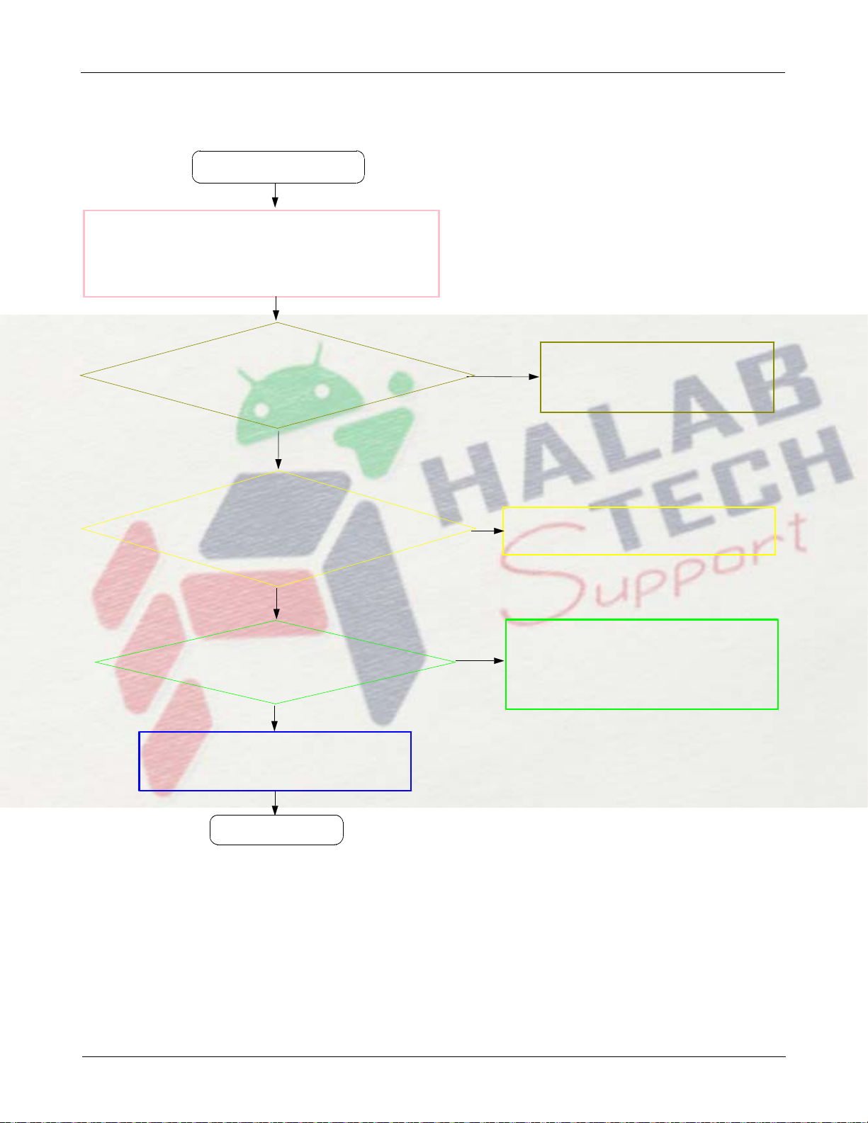
8-3-3.
No Service
No service
Yes
Check memu setting
Menu→applications→setting→wireless and network
mobile networks→network mode→setting is auto mode
Menu→Phone→Keypad
*#1234#
check Phone version
→
PHONE:I9295XXXX or
PHONE:unknown
PHONE:unknown
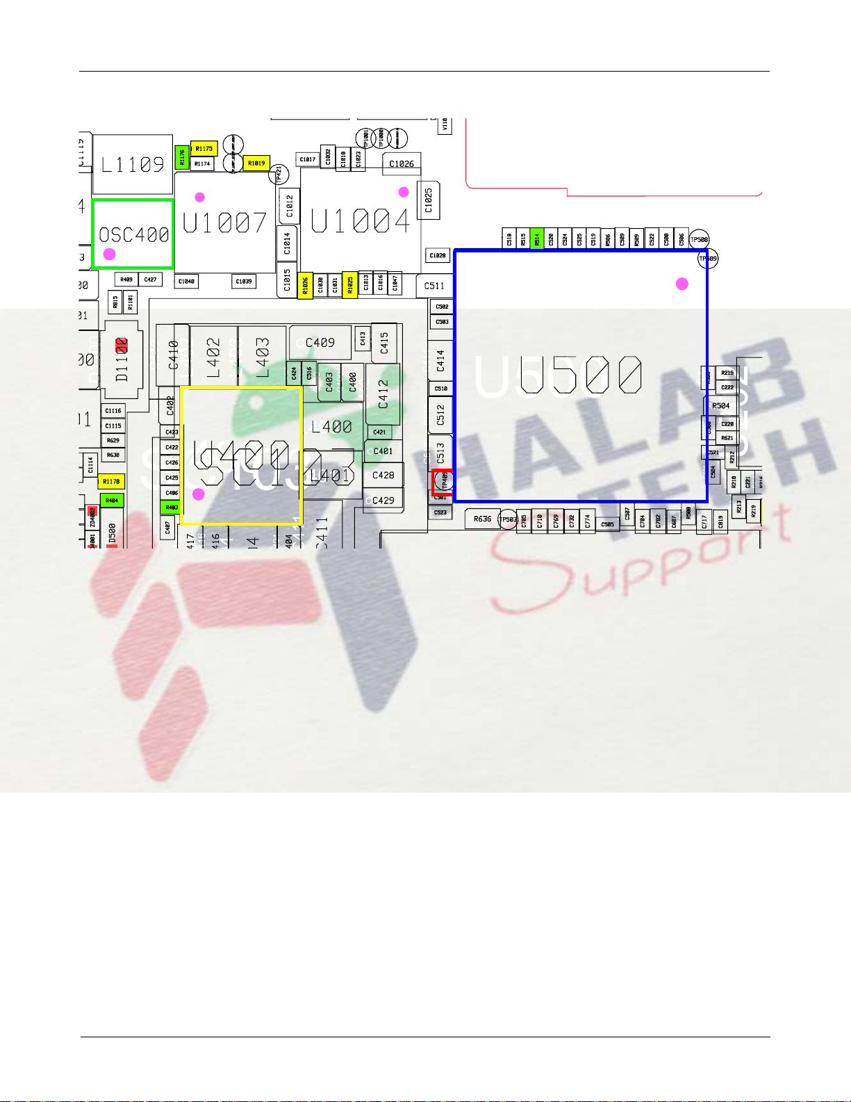
Check the voltage level
TP409=HIGH
(1.8
→
→
V)
→
?
PHONE:I9295XXXX
Check the connection of RF coaxial cable
No
Replace the U400
Check OSC400
Frequency
Replace U 500
END
Yes
= 19.2
Yes
Yes
MHz
No
Replace the OSC400
8-11
Confidential and proprietary-the contents in this service guide subject to change without prior notice.
Distribution, transmission, or infringement of any content or data from this document without Samsung’swritten authorization is strictly prohibited.
Level3Repair
8-12
Confidential and proprietary-the contents in this service guide subject to change without prior notice.
Distribution, transmission, or infringement of any content or data from this document without Samsung’swritten authorization is strictly prohibited.
Level3Repair
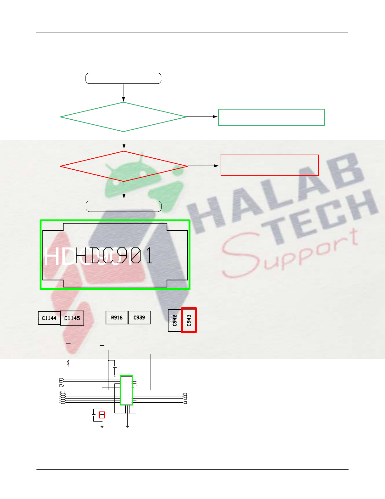
8-3-4.
Sim Part
Insert SIM card
Yes
Check the connection of
HDC901
Yes
Check the SIM Voltage.
C943
>= 1.8or3.0?
Yes
END
No
No
Connect SIM FPCB again
Replace the SIM FPCB
NFC_ANT_1
NFC_ANT_2
T_FLASH_CLK_2P9V
T_FLASH_DETECT
T_FLASH_D(3)_2P9V
T_FLASH_D(2)_2P9V
T_FLASH_D(1)_2P9V
T_FLASH_D(0)_2P9V
T_FLASH_CMD_2P9V
VREG_S4_1P8
R916
VREG_L6_2P9
NFC_SIMVCC
C943C942
C939
10
12
14 14
16
18
22
24
HDC901
2
2
4
4
66
8
8
10
12
16
18
2020
22
24
NC
NC
2728
VREG_L6
1
1
3
3
5
5
7
7
9
9
11
11
13
13
15
15
17
17
19
19
21
21
23
23
NCNC
25
26
SIM_IO
SIM_CLK
SIM_RST
NFC_SWP
8-13
Confidential and proprietary-the contents in this service guide subject to change without prior notice.
Distribution, transmission, or infringement of any content or data from this document without Samsung’swritten authorization is strictly prohibited.
Level3Repair
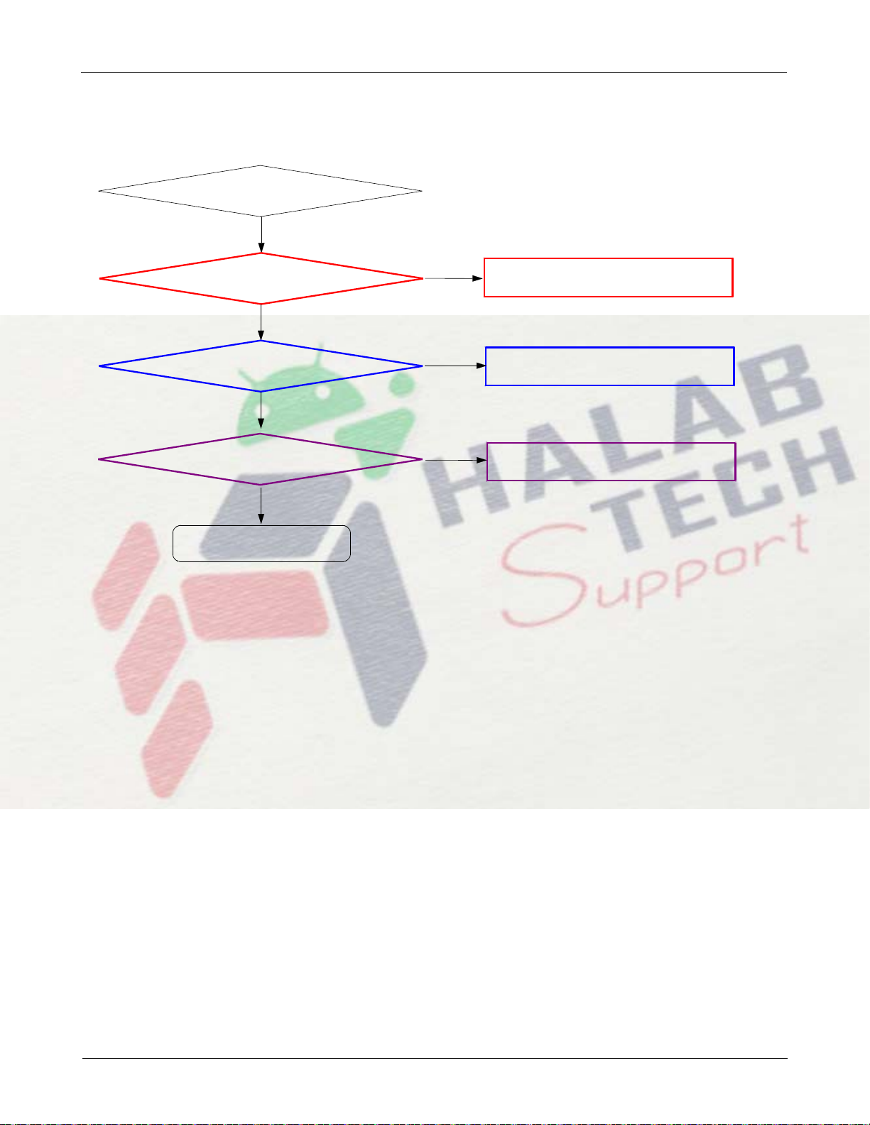
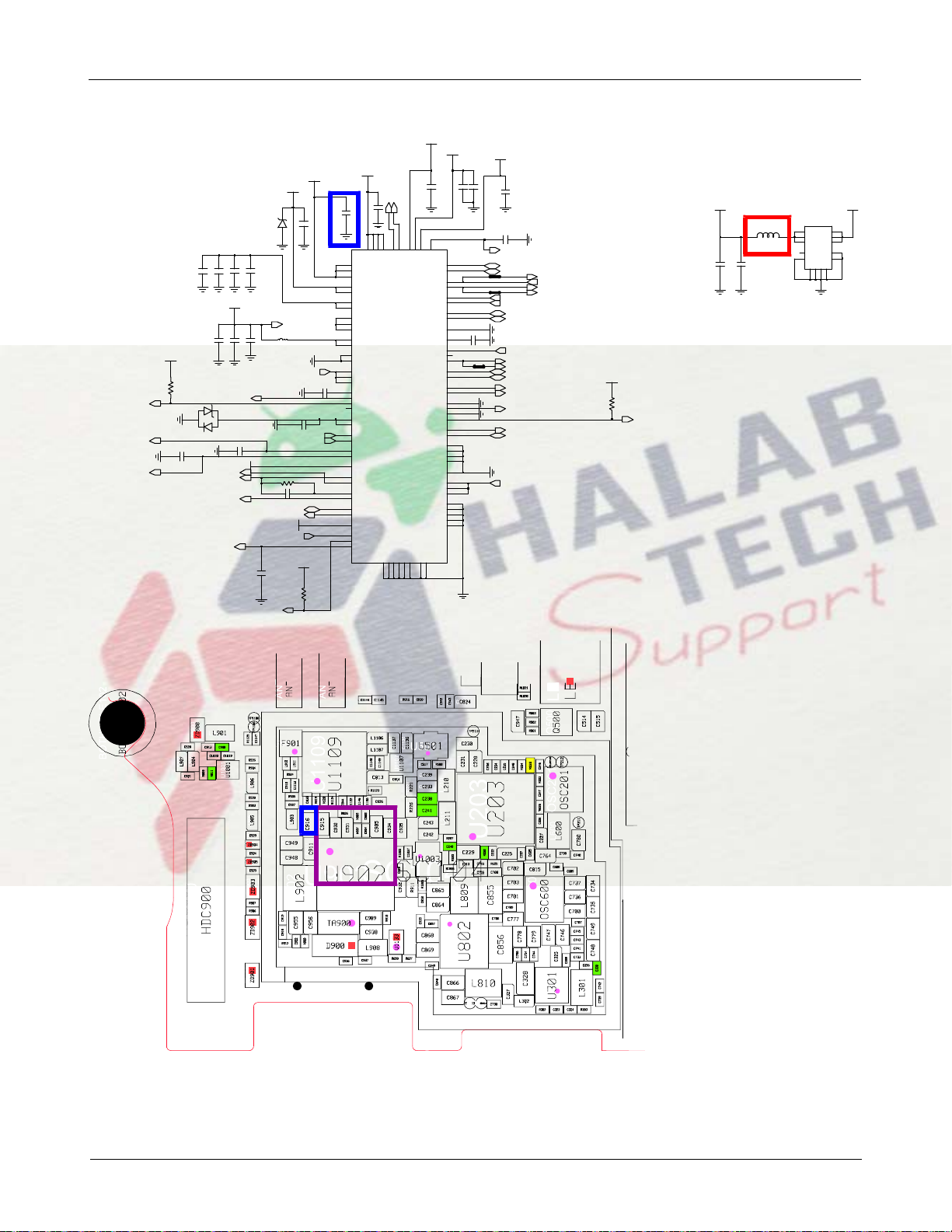
8-3-5.
Charging Part
Charging Sequence Start
Check the CHG_IN_5V(C911)=5V
Battery is Charging?
TA/USB Insert
Yes
VBUS_5V
=5V
Yes
Yes
Yes
No
No
No
Check L900=5V,
or may not connected TA/USB
Resolder and Replace U901
Resolder or Replace U902
END
8-14
Confidential and proprietary-the contents in this service guide subject to change without prior notice.
Distribution, transmission, or infringement of any content or data from this document without Samsung’swritten authorization is strictly prohibited.
CHG_DET
USB_VBUS_AP_4.9V
USB_VBUS_CP_4.9V
VPH_PWR
9
0
9
R
C931
PM8917_PON_RESET_N
8
4
9
C
C955 C956
VDD_VIB_3.0V
MOTOR_P
MOTOR_N
VIB_PWM
9
4
9
C
VF_DETB
VPH_PWR
C930
6
5
1
1
9
9
C
C
8
1
9
C
LED900
IF_PMIC_SDA_1.8V
IF_PMIC_SCL_1.8V
3
3
9
C
0
0
9
D
Z
L902
VREG_S4_1P8
PHONE_ON_N
MUSB_INT
CHG_IN_5V
WPC_5V
3
1
9
C
PM_SYS_PWR
PM_SYS_PWR
FLASH_SET
FLASH_EN
R911
C932
VREG_S4_1P8
2
1
9
R
Level3Repair
VREG_S4_1P8
CHG_IN_5V
E
S
E
N
S
V_BATTERY
E
N
S
E
_
S
Y
_
C910
R
D
E
N
T
G
T
T
A
A
B
B
_
V
V
9
0
9
1
1
C
9
C
3
9
8
2
5
6
H
H
T
T
A
B
C1
CHGIN
D1
CHGIN
D2
CHGIN
B1
WCIN
B2
WCIN
E1
BYP_C
E2
BYP_C
C2
BYP_W
C3
BYP_W
D3
BYP_W
F1
CHGLX
G1
CHGLX
H1
CHGPG
J2
CHGPG
H4
SYS
J3
SYS
J4
SYS
G2
C922
AVL
F3
DETBATB
F2
INOKB
E3
WCINOKB
A5
FLED1
A6
C947
FLED2
B5
TORCHEN
B6
FLASHEN
A2
SAFEOUT1
A3
SAFEOUT2
H9
IN_MOT
H10
MDN
J9
MDP
G9
MGAIN
G10
MPWM
G6
SDA
F9
SCL
F6
VIO
D5
MRST1B
D4
INTB
D6
RESETB
8
5
6
J
J
H
B
H
T
T
T
P
O
N
I
T
T
T
S
S
V
_
A
A
A
_
M
T
B
T
B
B
A
A
B
B
U902
G
A
Q
D
A
_
M
_
_
F
_
D
D
D
D
D
D
N
N
N
N
N
N
G
G
G
G
G
G
0
4
5
4
6
8
1
J
E
E
G
G
F
7
E
H
C
S
T
G
A
U
F
B
_
B
T
V
V
T
M
M
A
B
DN1
DP2
UT1
UR2
SL1
SR2
COMN1
COMP2
BC
MIC_USB
UID
IDB
JIG
ADN1
ADP2
AUT1
AUR2
QSTRT
VCELL
EO
ALRTB
SCLFG
SDAFG
TEST1
TEST2
TEST3
TEST4
VCC_TEST
SYS_A
SYS_A
SYS_Q
NC
NC
NC
NC
NC
C
C
N
N
1
2
VPH_PWR
5
4
0
0
2
9
9
1
C
C
9
C
C914
C919
V_BATTERY_SENSE
USB_HS_DM
USB_HS_DP
UART_TXD
UART_RXD
VPS_L_IF
VPS_R_IF
MUIC_DM
MUIC_DP
MUIC_ID
JIG_ON_N
JTAG_IF_CON_SENSE
USB_D_M
USB_D_P
CP_TXD_1.8V
CP_RXD_1.8V
V_BATTERY_SENSE
FUEL_SCL_1.8V
FUEL_SDA_1.8V
PM_SYS_PWR
JTAG_TXD
JTAG_RXD
VREG_S4_1P8
R910
FUEL_ALERT
A8
A9
E8
D8
E10
D10
B10
C10
C9
C8
B9
D9
C6
B7
A7
E7
D7
H7
G8
F8
J7
G7
F7
B3
C4
A4
B4
C5
F4
F5
E5
A1
A10
G3
J1
J10
VBUS_5V CHG_IN_5V
6
7
0
0
9
9
C
C
V
0
5
U901
L900
B3
A2
IN
OUT
C2
A3
IN
OUT
B2
C3
OUT
IN
B1
1
_ACOK
NC
C1
2
OVLO
NC
D
D
D
D
N
N
N
N
G
G
G
G
4
4
4
1
C
A
B
A
8-15
Confidential and proprietary-the contents in this service guide subject to change without prior notice.
Distribution, transmission, or infringement of any content or data from this document without Samsung’swritten authorization is strictly prohibited.
Level3Repair
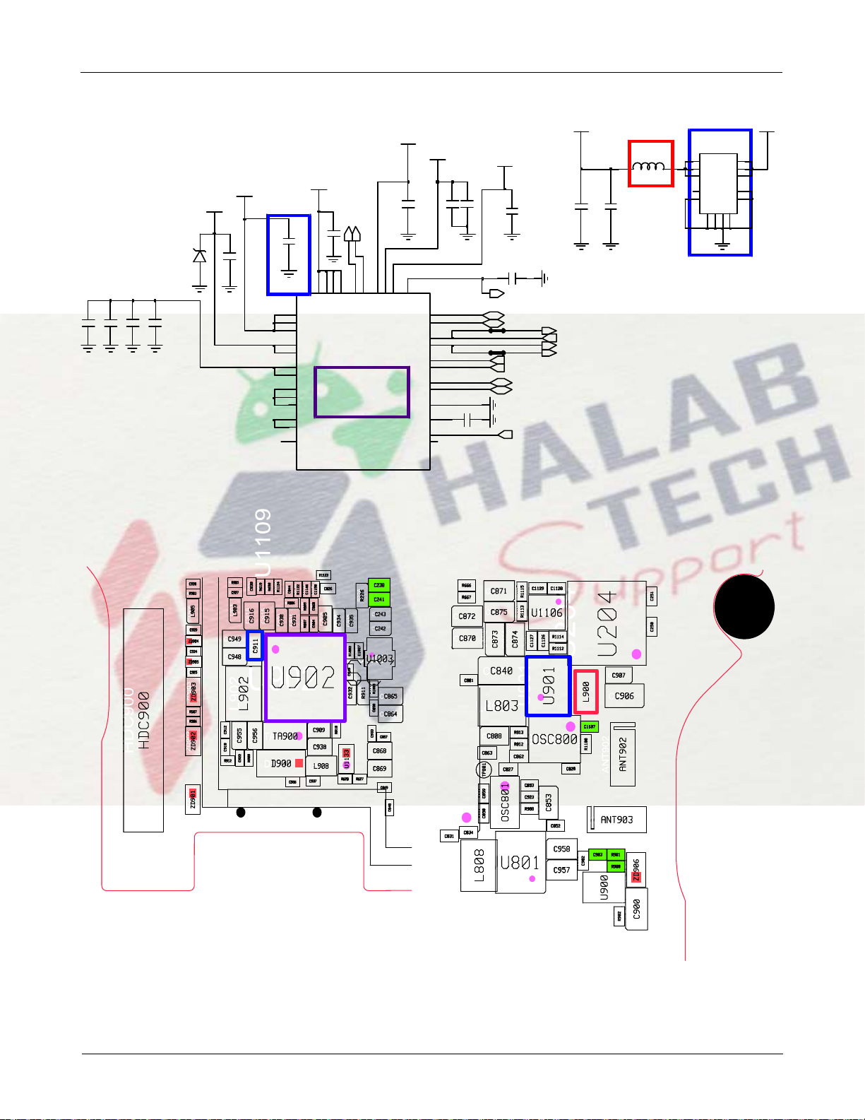
8-3-6.
OTG
OTG does not work
Yes
Check CHG_IN_5V(C911)=5V
Yes
Check VBUS_5V(L900)
Yes
Change the board
=5V
No
No
Check U902
Check U901
END
Yes
8-16
Confidential and proprietary-the contents in this service guide subject to change without prior notice.
Distribution, transmission, or infringement of any content or data from this document without Samsung’swritten authorization is strictly prohibited.
Level3Repair
VREG_S4_1P8
CHG_IN_5V
E
S
E
N
CHG_IN_5V
V_BATTERY
WPC_5V
1
1
0
0
9
D
Z
9
8
4
4
9
9
C
C
6
5
1
1
9
9
C
C
3
1
9
C
9
C
C1
CHGIN
D1
CHGIN
D2
CHGIN
B1
WCIN
B2
WCIN
E1
BYP_C
E2
BYP_C
C2
BYP_W
C3
BYP_W
D3
BYP_W
F1
CHGLX
G1
CHGLX
H1
CHGPG
J2
CHGPG
S
E
N
S
E
_
S
Y
_
R
D
E
N
T
G
T
T
A
A
B
B
_
V
V
9
0
9
C
2
5
H
T
T
A
B
3
6
5
6
J
J
H
H
H
T
T
T
P
N
T
T
T
S
S
A
A
A
_
_
T
B
B
B
T
A
A
B
B
U902
C910
7
8
9
8
E
B
C
H
S
T
O
G
I
A
U
F
V
B
_
B
M
T
V
V
T
M
M
A
A8
B
DN1
A9
DP2
E8
UT1
D8
UR2
E10
SL1
D10
SR2
B10
COMN1
C10
COMP2
C9
BC
C8
MIC_USB
B9
UID
D9
IDB
C6
JIG
VPH_PWR
6
7
0
0
9
9
C
JTAG_TXD
UART_TXD
UART_RXD
JTAG_RXD
C
5
4
0
0
9
9
C
C
2
1
9
C
C914
V_BATTERY_SENSE
USB_HS_DM
USB_HS_DP
VPS_L_IF
VPS_R_IF
MUIC_DM
MUIC_DP
C919
MUIC_ID
L900
V
0
5
B3
C2
C3
B1
C1
U901
IN
IN
IN
_ACOK
OVLO
D
D
N
N
G
G
1
4
A
A
A2
OUT
A3
OUT
B2
OUT
1
NC
2
NC
D
D
N
N
G
G
4
4
C
B
VBUS_5V CHG_IN_5V
8-17
Confidential and proprietary-the contents in this service guide subject to change without prior notice.
Distribution, transmission, or infringement of any content or data from this document without Samsung’swritten authorization is strictly prohibited.
Level3Repair
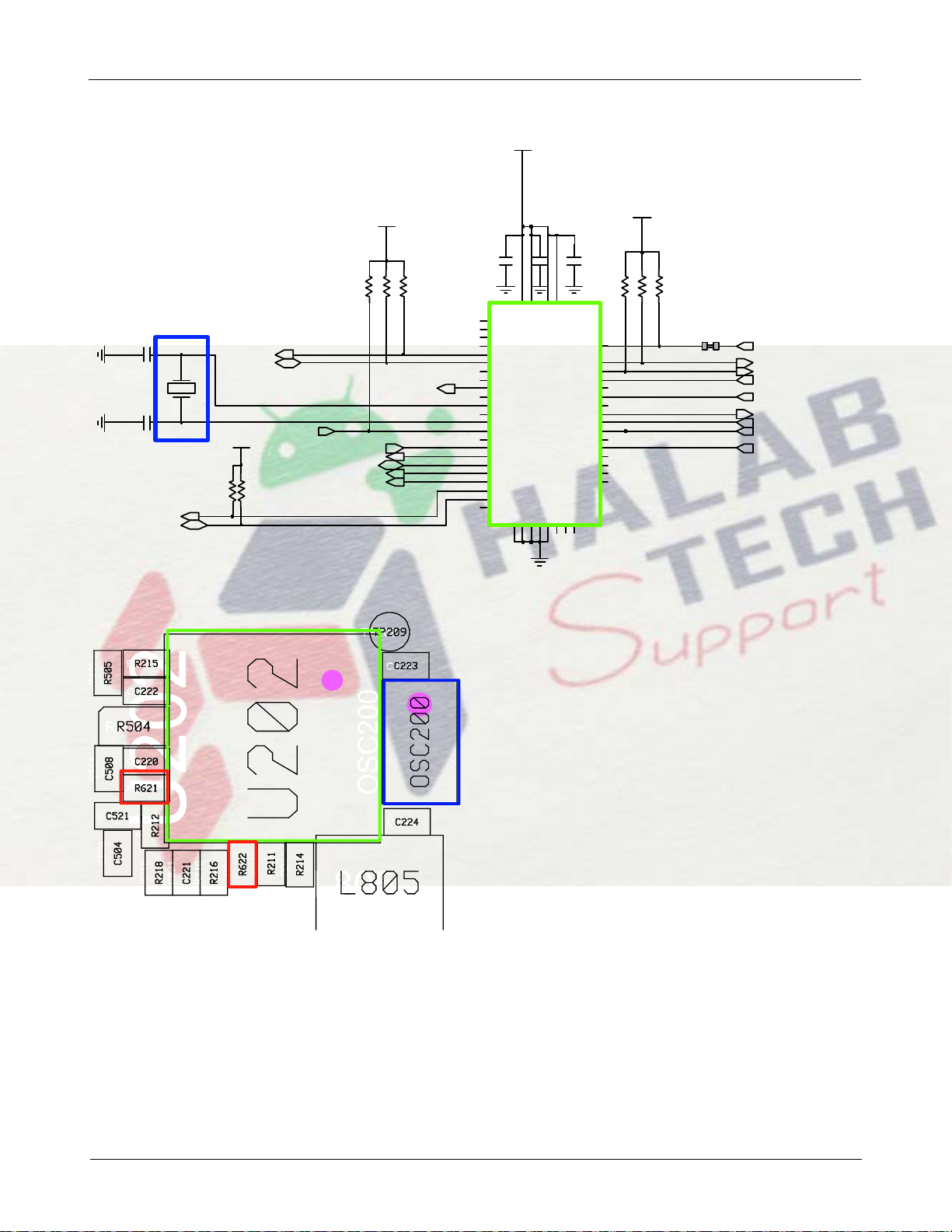
8-3-7.
Sensor
Sensor does not work
Yes
Check OSC200
Frequency
Check R621, R622
= 32.768
Yes
I2C is OK?)
(
Yes
khz
?
No
No
Replace OSC200.
Replace U202
Replace Sensor IC
Yes
END
8-18
Confidential and proprietary-the contents in this service guide subject to change without prior notice.
Distribution, transmission, or infringement of any content or data from this document without Samsung’swritten authorization is strictly prohibited.
VREG_LVS4_1.8V
Level3Repair
C223
C224
SENSOR_SCL_1.8V
SENSOR_SDA_1.8V
OSC200
RGB_SCL_1.8V
RGB_SDA_1.8V
VREG_LVS4_1.8V
R218
R219
MCU_CHG
M_SENSOR_INT
AP_MCU_SDA_1.8V
VREG_LVS4_1.8V
3
1
2
R
GYRO_DEN
GYRO_INT
ACC_INT2
1
1
2
R
2
1
2
R
MCU_TXD
A6
B6
A7
B3
D4
C5
B5
D5
A2
B2
C2
C3
G5
G1
D3
G6
G7
A5
C220
F5
F2
E3
F1
E2
VREG_LVS4_1.8V
C222
1
2
2
C
7
7
1
1
E
D
C
B
4
0
T
IN
0
0
U
D
O
O
O
I
I
D
D
D
D
V
PA00
D
D
D
V
V
U202
2
0
0
0
O
O
I
I
D
D
N
N
G
G
7
1
E
A
V
8
4
7
0
0
0
O
O
O
I
I
I
D
D
D
N
N
N
C
C
G
G
N
G
N
2
1
1
3
1
2
F
D
C
G
PA01
PA02
PA03
PA04
PA05
PA06
PA07
PA08
PA09
PA10
PA11
PA12
PA13
PA14
PA15
PA16
PA17
PA18
PA19
PA20
PA21
PA22
RESET_N
C
N
4
6
5
1
1
1
2
2
2
R
R
R
F6
B4
PB00
B7
PB01
A4
PB02
C4
PB03
F7
PB04
E6
PB05
F4
PB06
E4
PB07
G3
TP210
PB08
G4
PB09
E5
PB10
D2
PB11
A3
PB12
C6
PB13
D6
PB14
R217
SHORT
GES_LED_EN
MCU_nRST_1.8V
MCU_AP_INT_1.8V
MCU_AP_INT_2_1.8V
AP_MCU_SCL_1.8V
GYRO_DRDY
GES_SENSOR_INT
AP_MCU_INT_1.8V
ACC_INT1
8-19
Confidential and proprietary-the contents in this service guide subject to change without prior notice.
Distribution, transmission, or infringement of any content or data from this document without Samsung’swritten authorization is strictly prohibited.

Level3Repair
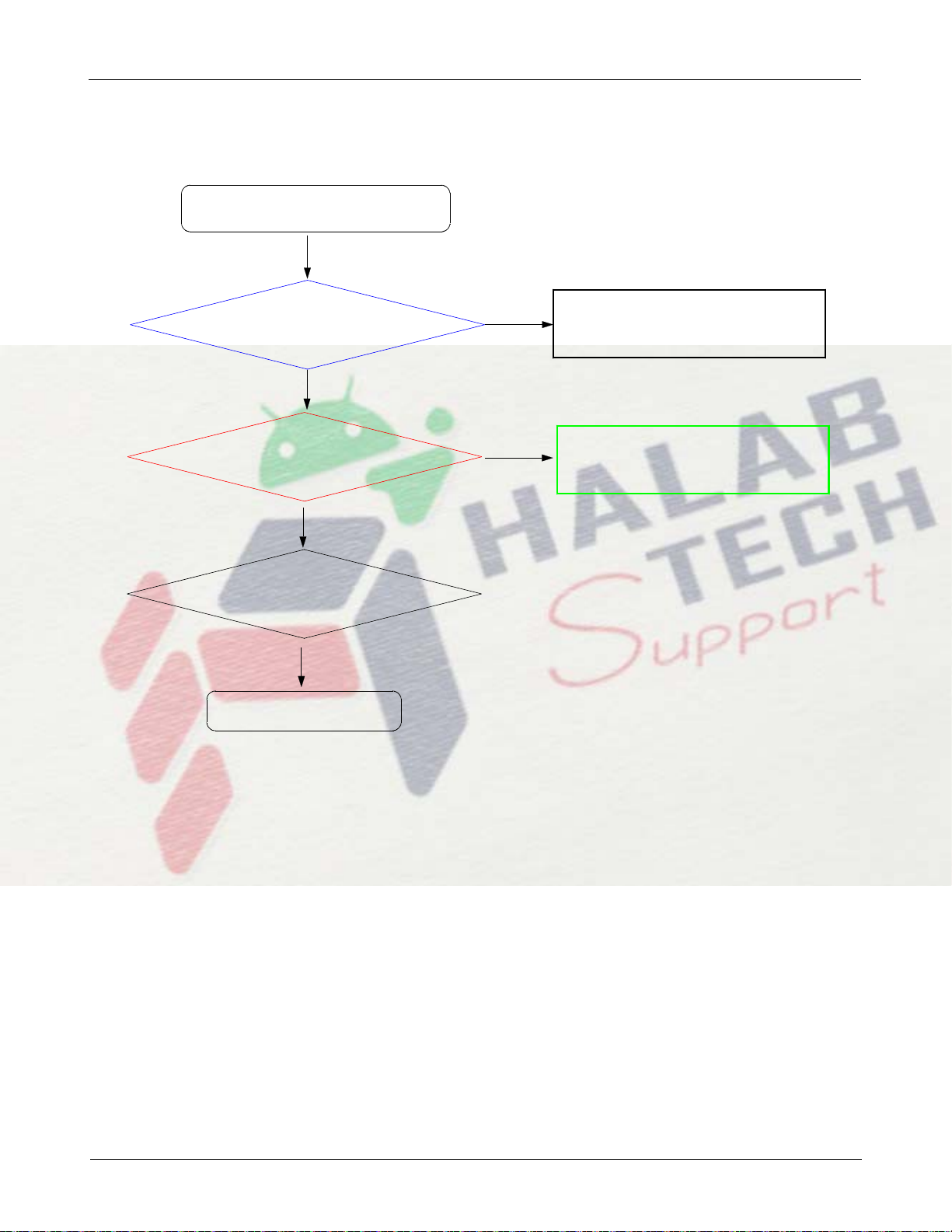
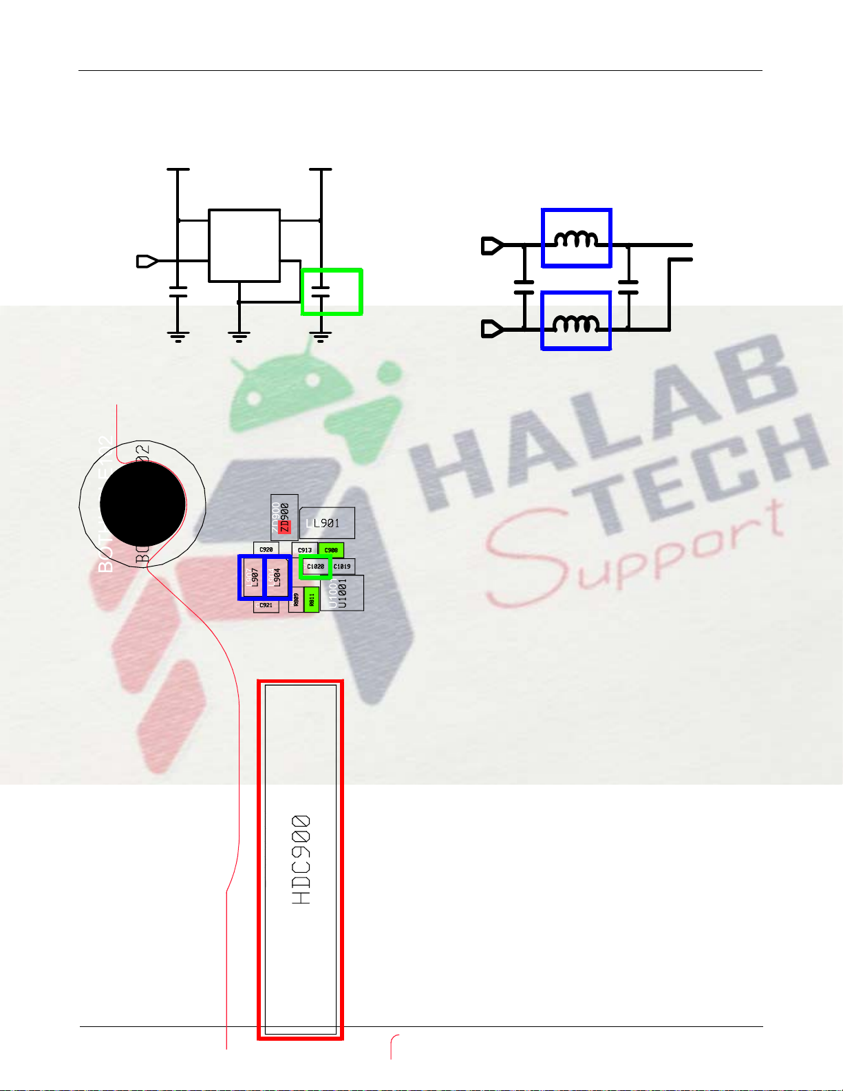
8-3-8-1
Microphone Part
Check main microphone function
in voice call Handset mode or voice recorder mode
Check sub board
connection(HDC900)
Check the voltage at
C1020
- Main MIC
Yes
Yes
=2.8V
No
No
Set the HDC900 connection
resolder or replace U1001
Yes
Check component soldering
statuses of L904, L907
Yes
END
No
Resolder or replace L904, L907
8-20
Confidential and proprietary-the contents in this service guide subject to change without prior notice.
Distribution, transmission, or infringement of any content or data from this document without Samsung’swritten authorization is strictly prohibited.
Level3Repair
VPH_PWR
MAIN_MICBIAS_2.8V
U1001
4
VDD
3
NE_SAIBCIM
C1019
CE
5
1
VOUT
2
GND
D
N
G
C1020
MAIN_MIC_N_CONN
L904
C921C920
L907
MAIN_MIC_P_CONN
8-21
Confidential and proprietary-the contents in this service guide subject to change without prior notice.
Distribution, transmission, or infringement of any content or data from this document without Samsung’swritten authorization is strictly prohibited.
Level3Repair
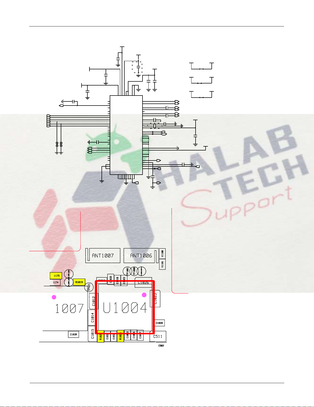
8-3-8-2.
Microphone Part-Sub(2nd) MIC
Check Sub(2n d) microphone function
in voice call loudSPK NS Off mode
or in camcording mode
Yes
Check PC B where Sub MIC
MIC1000) is placed
(
for any damage
Yes
Check the voltage at
C1006&C1017
=1.8V
No
No
Replace the PCB module
resolder or replace U1004
Yes
Check component soldering
statuses of L1000, L1002
Yes
END
No
Resolder or replace L1000, L1002
8-22
Confidential and proprietary-the contents in this service guide subject to change without prior notice.
Distribution, transmission, or infringement of any content or data from this document without Samsung’swritten authorization is strictly prohibited.
Level3Repair
8-23
Confidential and proprietary-the contents in this service guide subject to change without prior notice.
Distribution, transmission, or infringement of any content or data from this document without Samsung’swritten authorization is strictly prohibited.
Level3Repair
VREG_CDC_A
SUB_MICBIAS_LDO_1.8V
EAR_MIC_N
EAR_MIC_P
MAIN_MIC_N_CONN
MAIN_MIC_P_CONN
SUB_MIC_N
SUB_MIC_P
R1025
VREG_L25_1P225
C1017
R1026
EAROUT_FB
VREG_S4_1P8
C1016
EAROUT_L
EAROUT_R
C1030
71
70
67
68
55
66
54
58
48
52
53
59
50
61
45
56
62
60
65
57
12
17
18
27
15
38
21
20
37
C1013
7
4
0
1
C
6
2
MIC_BIAS1
MIC_BIAS2
MIC_BIAS3
MIC_BIAS4
MIC_IN1_M
MIC_IN1_P
MIC_IN2_M
MIC_IN2_P
MIC_IN3_M
MIC_IN3_P
MIC_IN4_M
NIC_IN4_P
MIC_IN5_M
MIC_IN5_P
MIC_IN6_M
MIC_IN6_P
MBHC_IN|MIC_IN7
MICB_CFILT1
MICB_CFILT2
MICB_CFILT3
HPH_LP
HPH_RM
HPH_REF
DMIC_CK0
DMIC_CK1
DMIC_CK2|RX_I2S_SD2
DMIC_D0
DMIC_D1
DMIC_D2|RX_I2S_SD1
2
3
3
G
I
D
_
D
D
V
D
N
G
3
1
3
1
6
4
O
P
I
_
A
D
C
_
D
L
V
O
D
|L
C
D
A
X
T
_
D
D
V
U1004
D
D
N
N
G
G
2
4
3
2
0
3
T
A
B
V
_
D
D
V
D
N
G
6
3
4
6
X
X
T
R
_
_
A
A
D
D
D
D
V
V
D
D
N
N
G
G
4
4
VPH_PWR
C1012
3
2
7
7
C
C
N
N
LINE_OUT1
LINE_OUT2
LINE_OUT3
LINE_OUT4
LINE_OUT5
SB_CK|TX_I2S_SD1
SB_DATA|TX_I2S_SD2
TX_I2S_SCK
TX_I2S_WS
RX_I2S_SCK
RX_I2S_WS
LDOH_CAP
P
M
O
C
X
C
T
_
_
D
D
D
N
N
N
G
G
G
9
9
5
6
4
3
CP_C1_M
CP_C1_P
CP_VNEG
CP_VPOS
INTR_OUT
RESET_N
EARO_M
EARO_P
CDD_CP
I2C_SCL
I2C_SDA
CCOMP
MODE0
MODE1
MCLK
GND_CCOMP
VREG_CDC_RXTX
4
1
0
1
C
28
23
46
39
40
34
29
7
C1025
1
6
8
C1028
3
11
TP1000
5
TP1001
22
16
10
4
14
19
9
31
43
51
47
42
25
TP_CODEC_RESET_N
C1032
5
1
0
1
C
C1018
C1023
C1026
SLIMBUS1_CLK
SLIMBUS1_DATA
CODEC_INT_N
CODEC_RESET_N
GND_CCOMP
VREG_S4_1P8
VREG_L34_2P2
VREG_L25_1P225
RCV_N
RCV_P
VPS_R
SPK_R
SPK_L
VPS_L
VREG_CDC_CP
1
3
0
1
C
VREG_CDC_CP
VREG_CDC_RXTX
VREG_CDC_A
C1029
VREG_S4_1P8
SLIMBUS1_MCLK
8-24
Confidential and proprietary-the contents in this service guide subject to change without prior notice.
Distribution, transmission, or infringement of any content or data from this document without Samsung’swritten authorization is strictly prohibited.

Level3Repair
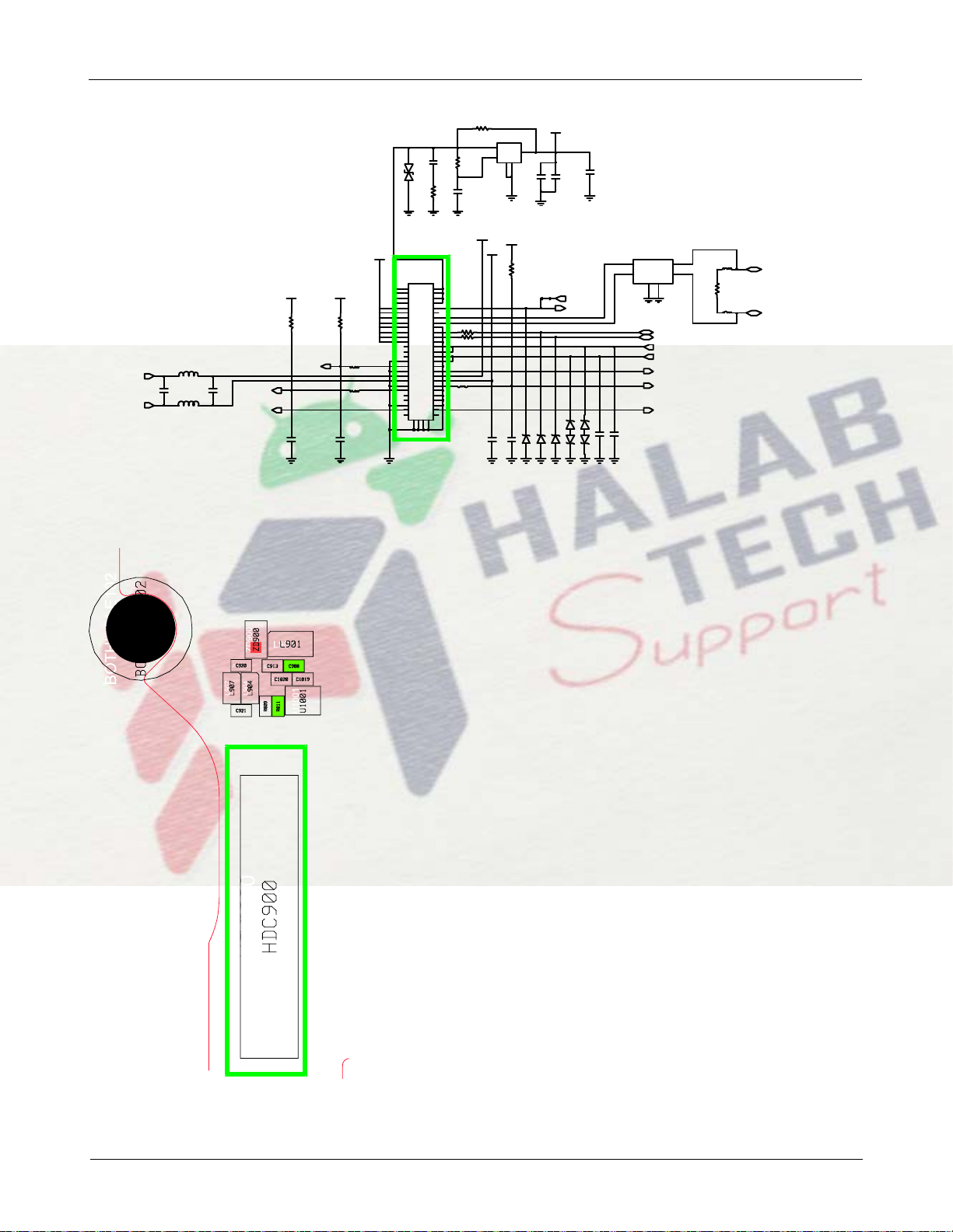
8-3-9.
Speaker Part
Yes
Check the connection of
HDC900
Yes
Replace the speaker
Yes
END
No
Reconnect HDC900
8-25
Confidential and proprietary-the contents in this service guide subject to change without prior notice.
Distribution, transmission, or infringement of any content or data from this document without Samsung’swritten authorization is strictly prohibited.
Level3Repair
MAIN_MIC_N_CONN
MAIN_MIC_P_CONN
R900
1
1
0
9
R
3
0
9
C
MAIN_MICBIAS_2.8V
VREG_L14
R906
R907
L905
3
VREG_S4_1P8
9
2
9
C
0
0
9
C
6
0
9
D
Z
2
0
9
R
VBUS_5V
HDC900
11
VREG_S4_1P8
R904
L904
C920
C921
L907
BACK_KEY
OK_KEY
VREG_S4_1P8
R905
L903
L906
MAIN_THM
6
2
9
C
7
2
9
C
44
55
66
7788
99
10
10
1112
11
12
1314
13
14
1516
15
16
1718
17
18
192220
19
20
2122
21
22
2324
23
24
25
26
25
26
2728
27
28
293330
29
30
3132
31
32
3334
33
34
3536
35
36
3738
37
38
39
40
39
40
41
42
4142
43
44
4344
45
46
4546
47
48
47
48
49
50
49
50
5152
51
52
535354
54
5
6
7
8
5
5
5
5
5
6
7
8
5
5
5
5
U900
IN
EN
V_BATTERY
4
OUT
D
D
N
N
G
G
5
2
C958
C957
R903
JTAG_USB_ID
MUIC_ID
2
0
9
C
F901
1
4
I|O
I|O
23
I|O
I|O
D
D
N
N
G
G
6
5
MUIC_DM
MUIC_DP
SPK_OUT_N
SPK_OUT_P
L911
MHL_DP
R924
L912
MHL_DM
MHL_ID
MENU_KEY
2
2
8
2
2
1
3
9
0
0
0
C
9
9
9
D
D
D
Z
Z
Z
C924
4
5
1
1
0
0
9
9
D
D
Z
Z
MDM_SUB_SEL1
C925
8-26
Confidential and proprietary-the contents in this service guide subject to change without prior notice.
Distribution, transmission, or infringement of any content or data from this document without Samsung’swritten authorization is strictly prohibited.
Level3Repair
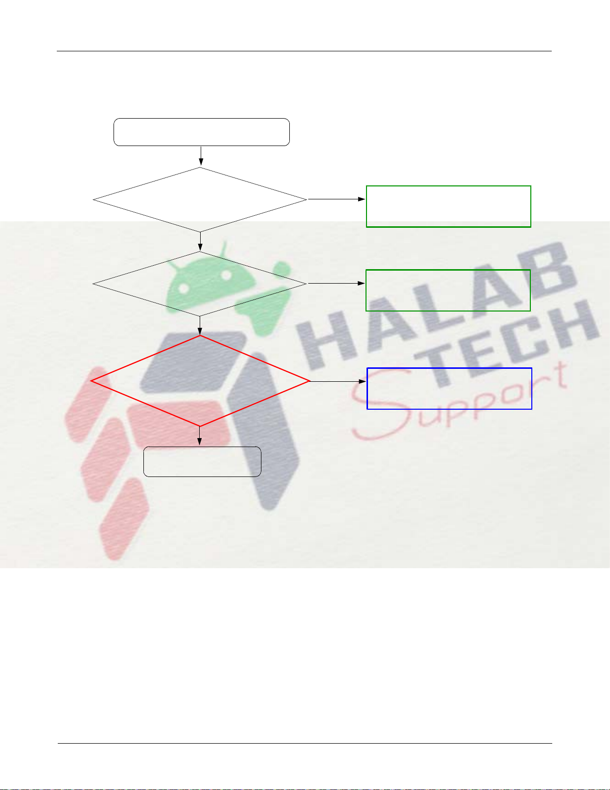
8-3-10.
Receiver Part
in voice call receiver mode.
Check RCV module where
Check receiver function
Yes
Check the soldering of
ANT1006, ANT1007
Yes
RCV's placed
for any damage
Yes
Check the signals on
V1100, V1101
No
Replace the PCB module
No
Replace the RCV module
No
Resolder or replace U1004
Yes
END
8-27
Confidential and proprietary-the contents in this service guide subject to change without prior notice.
Distribution, transmission, or infringement of any content or data from this document without Samsung’swritten authorization is strictly prohibited.
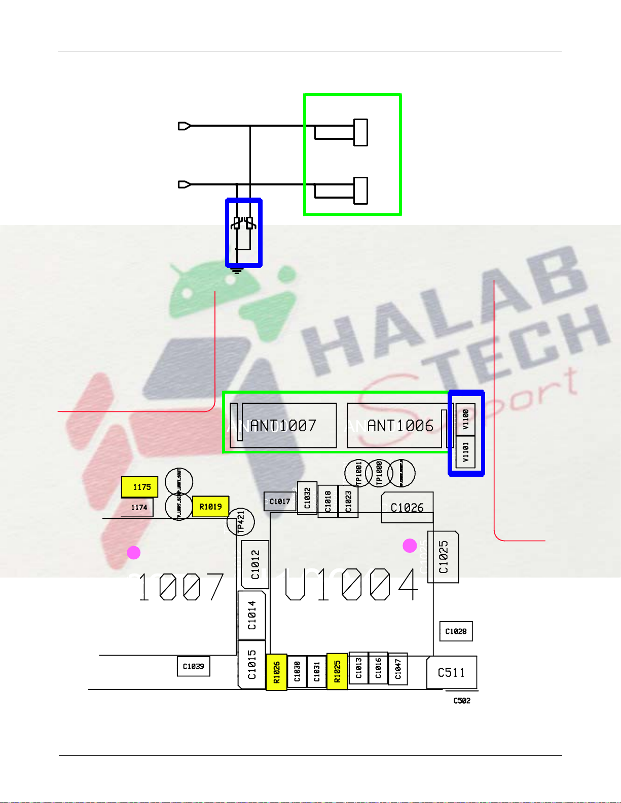
Level3Repair
RCV_P
RCV_N
ANT1006
1
1
2
2
ANT1007
1
1
2
2
1
0
0
0
1
1
1
1
V
V
8-28
Confidential and proprietary-the contents in this service guide subject to change without prior notice.
Distribution, transmission, or infringement of any content or data from this document without Samsung’swritten authorization is strictly prohibited.

Level3Repair
8-3-11.
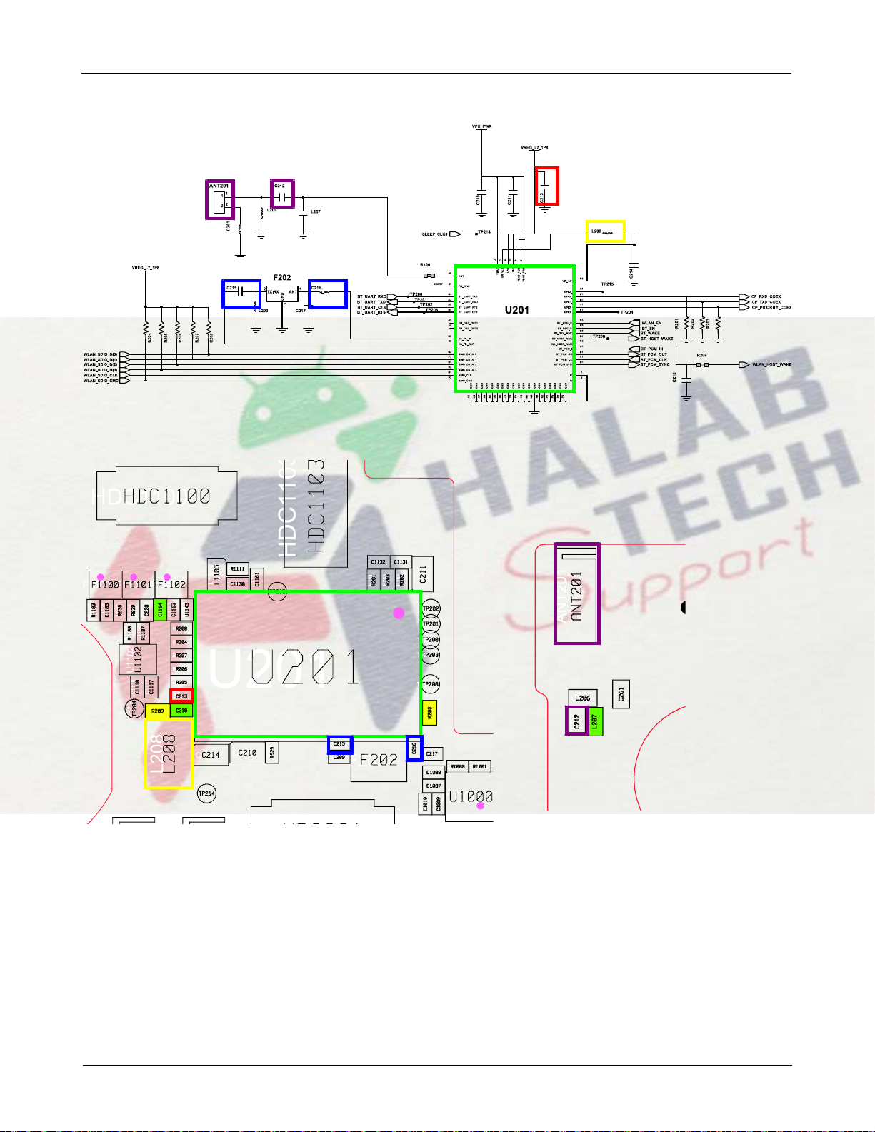
BT/WIFI
Check the Voltage on C213
Check the Voltage on L208
BT/WiFi is not working
Yes
Check BT or WiFi function
ON
Yes
1.8V
Yes
1.5V
Yes
No
=
=
No
No
Check the U800(crack, open, damaged, etc.)
Enable BT or WiFi Function
Resolder or change the L208
Check the Status of
C215, L216
Yes
Check the Status of
ANT201, C 212
Yes
Resolder or Replace U201
Yes
END
No
No
Resolder or change the C215, L216
Resolder or Replace ANT201, C212
8-29
Confidential and proprietary-the contents in this service guide subject to change without prior notice.
Distribution, transmission, or infringement of any content or data from this document without Samsung’swritten authorization is strictly prohibited.
Level3Repair
8-30
Confidential and proprietary-the contents in this service guide subject to change without prior notice.
Distribution, transmission, or infringement of any content or data from this document without Samsung’swritten authorization is strictly prohibited.
 Loading...