

SAMSUNG FAXF4300CXEU Service Manual

SF4300C
INKJET PRINTER COMPOUND CONTENTS
1. Precaution
2. Referential Information
3. Specifications
4. Disassembly & Assembly
5. Circuit
6. Repair
7. Exploded View
8. Packing
9. Circuit Diagram & Parts List
10. Block Diagram
11. PCB Layout
12. Wiring Diagram
SER VICE
Manual

ELECTRONICS

Samsung Electronics 1-1
1. Precautions
1-1 Safeguards
Please read these instructions carefully and completely.
1. Unplug this product from the wall outlet before
you disassemble it.
2. Replace defective parts with the same parts as
them.
3. Check the insulation of electricity-conducting
parts (metal plate or input terminal) that can easily contact AC plug blades.
4. How to check insulation: Pull the AC plug out of
the outlet and measure insulation resistance of
each blade.
5. Insulation resistance of AC plug blades against
electricity-conducting parts should be 1 megaohm
or over.
6. Always use it after connecting the ground of measuring instruments to the ground of chassis. And
after you use it, separate the ground of the
measuring instruments lastly.
1. Do not use this product in a humid place nor outdoor.
2. Do not place this product on an unstable stand or
table. The product may fall, causing serious damage to the product.
3. Use this product in a well-ventilated place.
4. Slots are provided for ventilation. Never push
objects of any kind into this product through
these slots as they may result in a fire or electric
shock. Never spill liquid of any kind on the product.
5. Power-supply cords should be routed so that
they are not likely to be walked.
6. Use this product in a place big enough to support
printers.
7. Install this product within 180cm from the computer and 150cm from the power outlet.
8. This product should be operated only from the
type of power source indicated on the marking
label.
9. If you use extension cords, be sure they have
three-wire grounding-type power outlets. Do not
overload wall outlets and extension cords. Never
load one wall outlet with over 15 ampere.
10. Unplug this product from the wall outlet before
cleaning. Do not use liquid cleaners or aerosol
cleaners. Use a dry cloth for cleaning.
11. Use only standard paper, OHP film, andapproved envelopes.
1-2 Servicing Precautions
Please read these instructions carefully and completely.

1-2 Samsung Electronics
1-3 Static Electricity Precautions
Semi-conductors are easily damaged by static electricity. They are usually called electrostatically
sensitive devices (ESD). For example, there are IC,
FET, and semi-conductor chips.
1) Before you handle semi-conductor parts, be sure
to discharge electricity by touching earth connection or putting on a wristband. (Before you turn
on the product, put off the wristband to prevent
electric shock.)
2) Remove the static electricity protective device
and then place the assembly on the surface of
electric conductors such as aluminum foil to
prevent static electricity from accumulating.
3) Do not use chemicals like Freon. These chemicals
produce static electricity that may damage parts.
4) Solder ESD parts with a grounded soldering iron.
5) Use static electricity protective solder. Solder not
marked Ôstatic electricity protectiveÕ may accumulate static electricity that damages ESD parts.
6) Do not get rid of the static electricity protective
cover of ESD parts until you are ready to replace
them. Most of ESD parts are packed, with electricity conducting materials in contact with ESD
parts leads.
7) Make static electricity protective materials contact the chassis or the circuit where parts will be
mounted, before you remove the materials from
ESD parts to be replaced.
8) Minimize your motion when you handle the ESD
parts from which static electricity protective
materials have been removed. Static electricity is
generated when your clothes are frictionized or
you walk on the carpet.
9) Be careful not to bend pins when you handle IC.
10) Pay attention to directions when you mount
parts on PCB.
11) Overheat during soldering may damage the
parts completely. Heat affects all the parts.

Samsung Electronics 2-1
2. Referential Information
2-1 Abbreviations & Acronyms
Abbreviations Definition
MFP Multi Function Peripheral
I/F INTERFACE
UART Universal Asynchronous Receiver/Transmitter
ECP Expended Capasilities port : 8bits Data
CR Carriage Return
LF LINE FEED
CIP COLOR IMAGE PROCESSOR
CCD Charge Coupled Device
A/D ANALOG TO DIGITAL
D/A DIGITAL TO ANALOG
LIU Line Interface Unit
TIT Transformer Input from Transformer
ROT Receive Output Transformer
LI Line Input

2-2 Samsung Electronics
2-2 Location & Outline of Pins of Electrical Parts
1. Gate 2. Drain 3. Source
1
2
3
C
E
B
R1 R2
R1=10KΩ
R2=0.6KΩ
.
.
.
.
TO-220
1. Base 2. Emitter 3. Collector
1
3
2
SOT-23
1. Base 2. Collector 3. Emitter
1
2
3
SOT-89
LOGIC AND CONNECTION
DIAGRAMS DIP (TOP VIEW)
Vcc
EB1
20 19 18 17 16 15 14 13 12 11
12345678910
DIR
A1 A2 A3 A4 A5 A6 A7 A8 GND
B2 B3 B4 B5 B6 B7 B8
20
20
20
J SUFFIX
CERAMIC
CASE 732-03
1
N SUFFIX
PLASTIC
CASE 738-03
1
DW SUFFIX
SOIC
CASE 751D-03
1

Samsung Electronics 2-3
BLOCK DIAGRAM
8 DIP
8 SOP
Vcc
Q6 Q6
OUT 1
IN1(- )
IN1(+ )
Q12
GND
Q17
1
2
_
+
3
4
Q19
8
Vcc
OUT 2
7
6
_
+
IN2 (- )
IN2 (+)
5
IN(-)
IN(+)
Q1
Q8
Q2
Q3
Q4
Q9
C1
Q11
Q10
Q13
Q14
Q15
Q18
Q20
R1
R2
OUT
Q21

2-4 Samsung Electronics
PIN CONNECTIONS
Block Diagram Simplified Application
Audio
Input
Cj
0.1
Ri
3.0k
C2*
5.0uF
C1
1.0uF
Rf
75k
Vin
FC1
4
3
6
5
8
7
#2
_
+
#1
_
+
2
50k
This device contains 45 active transistors.
Rf
Rj
*=Optional
Differential Gian=2 x
50k
125k
FC2
1
Vcc
Vo1
Vo2
Speaker
CD
GND
Bias
Circuit
MC34119
Chip
Disable
8
1
8
8
1
1
P SUFFIX
PLASTIC PACKAGE
CASE 626
D SUFFIX
PLASTIC PACKAGE
CASE 751
(SO-8)
DTB SUFFIX
PLASTIC PACKAGE
CASE 948J
(TSSOP)
14DIP
BLOCK DIAGRAM
14SOP
1
1
OUT2
OUT1
Vcc
IN1(-)
IN2(-)
IN1(+)
+
_
+
_
+
_
+
_
IN2(+)
1
2
3
4
5
6
7
14
13
12
11
10
9
8
18
CD
27
FC2
FC1
36
45
Vin
(Top View)
Vo2
Gnd
Vcc
Vo1

Samsung Electronics 2-5
PIN CONFIGURATION (Top Views)
S
KM416C/V10(2)00BJ KM416C/V10(2)00BT
TO-92
1
VCC
2
DQ0
3
DQ1
DQ2
4
DQ3
5
6
VCC
7
DQ4
8
DQ5
9
DQ6
10
DQ7
11
N.C
12
N.C
13
W
14
RAS
*A11(N.C)
*A10(N.C)
15
16
17
A0
18
A1
19
A2
20
A3
21
VCC Vss
42
41
40
39
38
37
36
35
34
33
32
31
30
29
28
27
26
25
24
23
22
Vss
DQ15
DQ14
DQ13
DQ12
Vss
DQ11
DQ10
DQ9
DQ8
N.C
UCAS
UCAS
OE
A9
A8
A7
A6
A5
A4
Vcc
DQ0
DQ1
DQ2
DQ3
Vcc
DQ4
DQ5
DQ6
DQ7
N.C
N.C
N.C
W
RAS
*A11(N.C)
*A10(N.C)
A0
A1
A2
A3
Vcc
A15
A14
A13
A12
A11
A10
A9
A8
NC
NC
WE
RESET
NC
NC
RY/BY
NC
A17
A7
A6
A5
A4
A3
A2
A1
1
2
3
4
5
6
7
8
9
10
11
12
13
14
15
16
17
18
19
20
21
22
1
2
3
4
5
6
7
8
9
10
11
12
13
14
15
16
17
18
19
20
21
22
23
24
44
43
42
41
40
39
38
37
36
35
34
33
32
31
30
29
28
27
26
25
24
23
Vss
DQ15
DQ14
DQ13
DQ12
Vss
DQ11
DQ10
DQ9
DQ8
N.C
N.C
UCAS
UCAS
OE
A9
A8
A7
A6
A5
A4
Vss
48
47
46
45
44
43
42
41
40
39
38
37
36
35
34
33
32
31
30
29
28
27
26
25
A16
BYTE
Vss
DQ15/A-1
DQ7
DQ14
DQ6
DQ13
DQ5
DQ12
DQ4
Vcc
DQ11
DQ3
DQ10
DQ2
DQ9
DQ1
DQ8
DQ0
OE
Vss
CE
A0
1
2
3
1.Emitter 2.Base 3.Collector
A16
BYTE
Vss
DQ15/A-1
DQ7
DQ14
DQ6
DQ13
DQ5
DQ12
DQ4
Vcc
DQ11
DQ3
DQ10
DQ2
DQ9
DQ1
DQ8
DQ0
Vss
OE
CE
A0
1
2
3
4
5
6
7
8
9
10
11
12
13
14
15
16
17
18
19
20
21
22
23
24
48
47
46
45
44
43
42
41
40
39
38
37
36
35
34
33
32
31
30
29
28
27
26
25
A15
A14
A13
A12
A11
A10
A9
A8
NC
NC
WE
RESET
NC
NC
RY/BY
NC
A17
A7
A6
A5
A4
A3
A2
A1

2-6 Samsung Electronics
OUTPUT B
1
16
SENSE RESISTOR
Powerdip 12+2+2
(Plastic Package)
ORDER CODE:PBL3717A
Powerdip
12+2+2
PULSE TIME
Vs(B)
GND
GND
Vss
INPUT 1
PHASE
SO-20
2
3
4
5
6
7
8
15
OUTPUT A
14
Vs(A)
13
GND
12
GND
11
REFERENCE
10
COMPARATOR INPUT
9
INPUT
MULTIWATT-15
ORDERING NUMBERS:
ORDERING NUMBERS:
TEA3718SDP
TEA3718DP
TEA3718SP
(Multiwatt-15)
15
14
13
12
11
10
9
8
7
6
5
4
3
2
1
Note:HEATSINK SURFACE CONNECTED TO PIN B
Us
DUT B
SENSE
DUT A
PULSE TIME
Us
N.C.
GND
ALARM OUTPUT
REFERENCE
COMPARATOR INPUT
IN0
PHASE
IN1
Uss
TEA3718SFP
TEA3718SFP
OUT B
PULSE TIME
Us Us
N.C.
GND
GND
N.C.
Uss
IN1
PHASE
(SO-20)
1
2
3
4
5
6
7
8
9
10
ORDERING NUMBER : TEA3718SP
TEA3718DP
TEA3718SDP
(Powerdip 12+2+2)
20
SENSE
19
OUT A
18
17
N.C.
16
GND
15
GND
14
PRE-ALARM OUT
13
REFERENCE
12
COMPARATOR INPUT
11
IN0
PULSE TIME
OUT B
GND
GND
Uss
PHASE
1
2
3
Us
4
5
6
7
IN1
8
16
SENSE
15
OUT A
14
Us
13
GND
GND
12
11
REFERENCE
10
COMPARATOR INPUT
9
IN0

Samsung Electronics 2-7
1
2
3
4
5
6
7
8
9
10
11
12
13
14
15
16
17
18
19
20
21
22
23
24
25
26
27
28
29
30
31
32
33
34
35
36
37
38
39
40
nECS2
nECS1
nECS0
nWBE1
nWBE0
nWE
nOE
nCAS1
nCAS0
nRAS1
nRAS0
nRCS2
nRCS1
nRCS0
VCC6
GND6
ADDR21
ADDR20
ADDR19
ADDR18
ADDR17
ADDR16
ADDR15
ADDR14
ADDR13
ADDR12
ADDR11
ADDR10
ADDR9
ADDR8
ADDR7
ADDR6
ADDR5
ADDR4
ADDR3
ADDR2
ADDR1
ADDR0
VCC5
GND5
120
119
118
117
116
115
114
113
112
111
110
109
108
107
106
105
104
103
102
101
100
99
98
97
96
95
94
93
92
91
90
89
88
87
86
85
84
83
82
81
NC
NC
NC
NC
NC
NC
NC
NC
NC
NC
GND1
NC
NC
NC
NC
NC
NC
NC
NC
VCC1
NC
NC
NC
NC
NC
NC
NC
NC
GND2
GOP12
NC
NC
NC
NC
NC
NC
GPIO0/TCK
GPIO1/TMS
GPIO2/TDI
GPIO3/nTRST
121
122
123
124
125
126
127
128
129
130
131
132
133
134
135
136
137
138
139
140
141
142
143
144
145
146
147
148
149
150
151
152
153
154
155
156
157
158
159
160
VCC4
DATA15
DATA14
DATA13
DATA12
DATA11
DATA10
DATA9
DATA8
GND4
DATA7
DATA6
DATA5
DATA4
DATA3
DATA2
DATA1
DATA0
VCC3
245CLK
PPD0
PPD1
PPD2
PPD3
PPD4
PPD5
PPD6
PPD7
GND3
nSTROBE
nAUTOFD
nSLCTIN
nINIT
SELECT
nACK
BUSY
PERROR
nFAULT
VCC2
GPIO4/TDO
807978777675747372717069686766656463626160595857565554535251504948474645444342
41
nECS3
GOP0/TXD1
GIP0/RXD1
GOP1/TXD2
GIP1/RXD2
TEST1
TEST2
GIP5/UCLK
CLKSEL
nRESET
GND7
MCLK
GND8
GOP5/nIOWR1
VCC7
GIP2/nEINT1
GIP3/nEINT2
GIP4/nXDREQ
GOP2/nXDACK
NCNCNCNCNC
NC
EEDATA
EECLK
GND9
GOP3/TONE
GOP4/nRSTO
GOP8/nIORD2
GOP9/CLKOUT
GOP10/FIREPULSE
GOP11
GOP6/nIOWR2
GOP7/nIORD1
VCC8
NCNCNC
KS32C6200
160 TQFP
(Top View)
KS16116/7
1
2
3
4
5
6
7
8
9
10
11
12
13
14
15
16
17
18
19
20
D11
D10
D9
D8
VSS
D7
D6
D5
D4
VDD
D3
D2
D1
D0
VSS
ADDR4
ADDR3
ADDR2
ADDR1
ADDR0
60
59
58
57
56
55
54
53
52
51
50
49
48
47
46
45
44
43
42
41
VDD
GPO0
GPO1
GPO2
GPO3
VSS
GPO4
GPO5
GPO6
GPO7
VDD
GPI0
GPI1
GPI2
GPI3
VSS
GPI4
GPI5
GPI6
GPI7
GPIO0
GPIO1
GPIO2
GPIO3
GPIO4
GPIO5
GPIO6
GPIO7
VSS
Xin
Xout
VSS
VDD
nXDREQ
TEST
nXDACK
nRESET
nCIPCS
nRD
nWR
ADCDG
ADCDP
pVref
Vin
nVref
ADCAP
ADCAG
VSS
CLR-SCANSHCLK1
CLK2
CLK-M
VSS
VDD
VSS
D15
D14
D13
D12
212223 2425262728 29 3031323334 353637383940
807978 7776757473 72 7170696867 666564636261
CIP1
V2.1
1
2
3
4
5
6
7
8
9
10
11
12
13
14
15
16
17
18
19
20
21
22
23
24
25
26
27
28
29
30
GP03
GP04
GP05
GP06
GP07
GNDD
GNDD
D7
D6
D5
D4
D3
D2
D1
D0
GNDD
GNDA
RXAMPI
NC
NC
GNDA
V
DD
GNDD
SWGAINI
ECLKIN1
SYNCIN1
NC
NC
NC
GNDA
31 32 33 34 35 36 37 38 39 40 41 42 43 44 45 46 47 48 49 50
NCNCNC
DAIN
ADOUT
BYPASS
RCVI
TXATT3
TXATT2
TXATT1
NC
VREFN
VSSG
TXAO
RXAI
Vcc
GNDA
VC
AOUT
GNDD
GP02
SWGAINO
RCVO
GNDD
RLSD
RXDO
GP19
GP20
GNDD
GP21
SEPYO
GNDD
DAOUT
ADIN
SEPXO
SEPCLK
SEPCLKX
SEPWCLK
DCLK
GNDD
51
52
53
54
55
56
57
58
59
60
61
62
63
64
65
66
67
68
69
70
71
72
73
74
75
76
77
78
79
80
NC
IRQ
WRITE-R/W
CS
READ-ø2
RS4
RS3
RS2
RS1
RS0
GP13
NC
GP11
RTS
EN85
DGND
PORI
XTALI
XTALO
XCLKO
YCLKO
DVDD
DCLK
SYNCIN2
GP16
GP17
DGND
CTS
TXDI
GNDD
81828384858687888990919293949596979899100

2-8 Samsung Electronics
2-3 Chip Replacement (SMD parts)
2-2-1. Precautions for Chip Replacement
1. See to it that the soldering iron does not touch
parts directly. In particular, TSOP may be easily
damaged by heat.
2. Handle the soldering iron with care and avoid
using the same many times. Some parts can be
damaged by sudden heat. Preheat parts for minutes at about 100¡c before soldering them.
3. The temperature of the soldering iron should
remain at about 240¡c Use a 280¡c iron for
bigger parts.
4. Thin (0.3mm) solder used for chip parts does not
contain enough flux. Use additional flux.
* For computers and OA systems, water-soluble flux
is used. Water-soluble flux and solder are also
good for replacing parts and repairing this product. Improper flux may corrode the soldered part
and cause serious defects to the system.
5. Be careful not to damage the circuit pattern when
you disjoin soldering. The pattern should be clean
because there are a lot of pins close together on IC.
6. Be careful not to cause a short circuit between
close pins.
7. Locate parts in place. It has a great influence on
soldering.
8. Do not use repaired parts again.
9. Check the soldered part.
10. Defective variable resistors are not adjustable. Be
sure to replace them.
11. After finishing the job, check if there are cold soldered parts.
2-2-2. Tools to Replace Chips
The following tools are used to replace chip parts.
¥ iron with thin tip
¥ iron with small and flat tip
¥ solder remover
¥ ventilation device
¥ tools to lift flat parts
¥ flux that can be cleaned with water
¥ 0.3mm thin solder that can be cleaned with water
¥ wire to remove solder
¥ tweezers
2-2-3. Chip Resistance & Chip Condenser
2-2-3 (a) Type
There are the following types of chip resistance and
chip condensers.
¥ There are the following types of thin film and chip
condensers.
¥ Carbon Film chip resistance
¥ Metal Film chip resistance
¥ Chip ceramic condenser
¥ Chip variable resistance
2-2-3 (b) Removal
Use 2 soldering irons.
a. Use a thin-tip iron.
b. Keep about 280¡c
c. Apply heat to both ends of a part at the same time.
d. Remove it with the tip of the iron while heating.
e. Remove the remaining solder on PCB completely
with solder removing wire. It should be done to
install a new part.

Samsung Electronics 2-9
2-2-3 (c) Installation
a. Clean the place where a new part will be located.
b. Apply water-soluble flux.
c. Set a part correctly in place. Prevent it from shift-
ing.
d. Stick the part fast without contacting it directly
with the soldering iron. Put 0.3mm solder between
the iron and the part so that it can melt into the
part.
e. Check the soldered part with a magnifier.
2-2-4. Chip Tantalum Condenser and Chip Filter
2-2-4 (a) Type
There are the following types of chip tantalum condenser and chip filter.
¥ Chip coil
¥ Chip tantalum condenser
¥ Chip tantalum electrolysis condenser
¥ Chip aluminum electrolysis condenser
¥ Chip transformer
¥ Chip filter
2-2-4 (b) Remoral
1. Use a special solder-removing iron.
a. Choose an iron tip that suits the size of the part.
b. Put the iron tip to the part to be soldered.
c. Remove the part when solder melts.
d. Remove the remaining solder completely with
solder-removing wire.
2. Use two irons.
a. Use an iron with small flat tip.
b. Apply heat to both ends of the part at the same
time.
c. Remove the part with the tip of the iron while
melting.
d. Remove the remaining solder completely with
solder removing wire.
2-2-4 (c) Installation
1. Clean the place where new parts will be installed.
2. Apply water-soluble flux.
3. Locate a part exactly in place. Be careful not to shift
it.
4. Stick the part fast with a soldering iron not contacting it directly. Put 0.3mm solder between the
iron and the part so that it can melt into the part.
5. Check the soldered part with a magnifier.
2-2-5. Chip Variable Resistance, Chip
Variable Condenser, Diode &
Transistor
Chip Variable Resistance, Chip Variable Condenser,
Diode & Transistor
2-2-5 (a) Type
There are the following types.
¥ Chip Variable Resistance
¥ Chip Variable Condenser
¥ Diode
¥ Transistor
2-2-5 (b) Removal
Use two soldering irons.
a. Use an iron with small flat tip.
b. Apply heat to both ends of a part at the same time.
c. Remove the part with the tip of the iron while sol-
der melts.
d. Remove the remaining solder completely with sol-
der removing wire.
2-10 Samsung Electronics
2-2-5 (c) Installation
1. Clean the place where new parts will be installed.
2. Apply water-soluble flux.
3. Locate a part exactly in place. Be careful not to shift
it.
4. Stick the part fast with a soldering iron not contacting it directly. Put 0.3mm solder between the
iron and the part so that it can melt into the part.
2-2-6. Chip IC
2-2-6 (a) Type
There are the following types of chip IC.
1. SOP (Small Outline Package) IC
2. SSOP (Shrink Small Outline Package) IC
3. VSOP (Very Small Outline Package) IC
4. QFP (Quad Flat Package) IC
5. VQFP (Very Quad Flat Package) IC
6. PLCC (Plastic Leaded Chip Carrier) IC
7. TSOP (Thin Small Outline Package) IC
2-2-6 (b) Removal
1. Use a special solder-removing iron.
a. Choose an iron tip that suits the shape and the
size of IC.
b. Use ÔthinÕ tip to contact legs of IC.
c. Put the tip right in front of the legs of IC.
d. Twist the iron carefully when solder melts.
e. Raise and remove IC.
2. Use a ventilation device.
a. Choose an injector that suits IC.
b. Choose the temperature and the ventilation
speed. (normal: temperature - 7, speed - 4)
c. Use IC-removing tools.
d. Preheat it for about 5 seconds with the ventila-
tion device. And apply heat with the injector
until IC can be removed from the board with IC
removing tools.
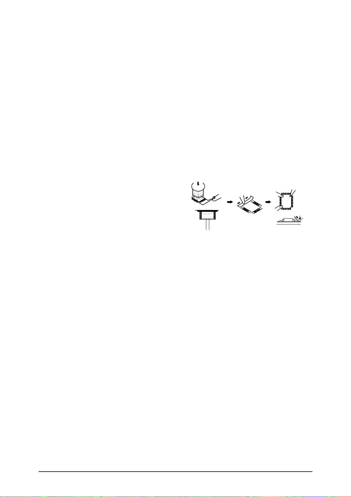
2-2-6 (c) Installation
1. Remove the remaining solder completely with solder-removing wire.
2. Clean the place to be soldered.
3. Apply water-soluble flux.
4. Put IC in place and solder the legs of opposite
direction.
5. Solder each leg carefully with thin tip.
6. Remove solder with solder-removing wire if there
is a short circuit.
7. Check the soldered part with a magnifier.
IC

Samsung Electronics 3-1
3. Specifications
3-1 Specifications
Specification & Features
1. Printer
1-A. Set
1-B. Ink Cartridge Supply
Technology
Thermal Inkjet
1-pen & print head swapping type
Speed
Color 3PPM at draft mode (6005300 DPI)
Mono 7PPM at draft mode (6005300 DPI)
Resolution
Color 600 5 600DPI (120051200 DPI addressable)
Mono 600 5 600DPI (120051200 DPI addressable)
Printing Width 8 Inch
Feeding
Automatic 100 sheets for normal cut sheets, coating paper
Method
Manual Recommended for thick media, fashion paper, envolope,
postcard, Banner paper
Emulation Host Based Printing (GDI)
Printer Driver Window 3.1/3.11 and Windows 95 drivers
Interface IEEE 1284 Compatible Parallel Interface (ECP)
Mono Ink Color Ink
Print Head 208 nozzles 192 nozzles
Ink Type Pigment Dye
Ink Color Black Color
Ink Yield About 600 sheets About 200 sheets
3-2 Samsung Electronics
2. Scanner
Technology CCD
Scanner Type Color/Mono
TWAIN Compatible Yes
Pre-Scan Using Carrier Sheet
Speed Color about 1 PPM
Mono about 2 PPM
Resolution Color 300 X 300 DPI (for SmartJet-C only)
Mono 300 X 300 DPI
Gray Scale 256 Level
Printing Width 8 lnch
Feeding Manual Yes
Interface IEEE 1284 Compatible Parallel Interface (ECP)

Samsung Electronics 3-3
3-1. Facsimile
Compatibility ITU-G3
Scan Method CCD Shuttle Scanning Method
Scan Width Max. 8.5 Inch, Effective : 8 Inch
Document Feeding Method Manual Feeding Method
Guide Document In-put Guide
Stacker None
Handset None
Keys on OPE 4EA (Ready, Cartridge, FF/STOP, START/COPY))
LEDs on OPE 3EA (Ready, Busy, Scan/Fax)
Real Time Clock None
Fax Monitoring Speaker Yes
Ring Volume Control Switch None
Paper Tray BIN Type, up to 100 sheets
Modem Speed Max 9600 bps
Coding Method MH, MR, MMR, Error Correction Mode
LCD None
Answering Machine I/F None
Extension Phone I/F 1-Jack, Extension Phone Transfer
PC Interface IEEE 1284 Parallel Interface (ECP)
Fax Send Resolution - Standard : 200 x 100 dpi
- Fine : 200 x 200 dpi
- Superfine : 300 x 300 dpi

3-4 Samsung Electronics
3-2. Facsimile
Feature Use Ext. Telephone Use PC
Gray Scale - Auto Contrast - Auto Contrast
- 256 level with
Error diffusion
Memory Transmission None Yes
Memory Rx Yes Yes
Receive Mode - Tel, Fax - Fax
- PC Rx
One Touch Dial *No 70 Numbers
Speed Dial *No
Chain Dial *No No
On Hook Dial *No No
Last Number Redial *No No
Telephone Auto Busy Redial *No No
No Power Operation *No No
Hold & Mute *No No
Pause *No Yes
Ring Volume Control *No No
Flash *No No
Tone/Pulse Switch *No Yes
Sensors No paper sensor, Paper jam sensor
Error Indicator Yes (On LED) Yes (On PC Screen)
Voice Request No No
Others TTI Yes
Rx Terminal ID No No
Polling No No
DRPD U.S.A : Yes, Other countries : No
Mercury No No
* The marked “No” can be provided by telephone’s feature.

Samsung Electronics 3-5
Feature Use Ext. Telephone Use PC
Tx/Rx Journal No Yes
Report & List
Delayed Dial List No No
Print out System Data No Yes
Tel Number List No Yes
Help List No No
Copy Yes (1-Page) Yes (99-Page)
Copy Gray Scale No Yes
Reduction Copy No Yes
Enlargement Copy No No
4. Electrical & Environment
Power Source AC 220~240V, 0.3A, 50~60Hz
Dimension (W5D5H) 422(mm) 5 237(mm) 5 180(mm)
Weight 3.7kg
5. Accessories
Tel Handset No
Curl Cord No
Tel Line Yes
Power Cord Yes
Software 1 CD-ROM
(Manual, Printer Driver, PC-Fax)
Manual 1EA
Ink Mono Ink Yes
Cartridge Color Ink Yes
* Xerox’s OCR S/W and scanner editor are recommended for its own use.

Samsung Electronics 4-1
4. Disassembly & Assembly
4-1 Taking Off Front Cover
This section explains with illustrations how to disassemble the printer.
It does not explain how to assemble it, because it is the very reverse of disassembly.
Fig.4-1. Taking Off Front Cover -1 Fig.4-1. Taking Off Front Cover -2
Disconnect power cords and printer cable from
the printer.
Unscrew 1 screws on rear cover to separate ink
cartridge storage.
Push Guide Extension in the direction of the
arrow symbol.
Remove 2 screws between front cover and bottom cover.
▲▲▲▲
Hold the upper part of front cover with both
hands and lift the front cover, holding
down rear cover.
Separate front cover from rear cover in the
direction of the arrow symbol.
▲▲

4-2 Samsung Electronics
4-2 Taking off Rear Cover
4-3 Separating Automatic Sheet Feeder
Fig.4-2. Taking Off Rear Cover
Push in the paper guide (ÒCÓ) of automatic
sheet feeder and place it inside of A4 line.
Push the guide manual(L) (ÒDÓ) left.
Unhook right and left hooks(ÒAÓ) on the upper
part of rear cover.
Unhook right and the left hooks of bottom
cover by pushing them in.
Separate rear cover in the same direction that
the automatic sheet feeder is mounted.
▲▲▲▲▲
Fig.4-3. Separating Automatic Sheet Feeder
Remove various wires fixed on the side of automatic sheet feeder.
Unscrew 2 screws on automatic sheet feeder.
Push slightly and disconnect the hook (ÒAÓ) fixed to the main frame.
Separate automatic sheet feeder by pulling it in the direction of the arrow symbol.
▲▲▲▲
“A”
Samsung Electronics 4-3
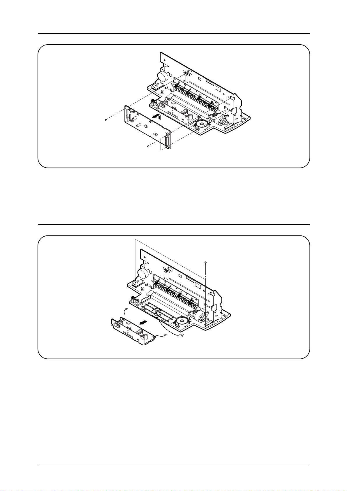
4-4 Separating Main Circuit Board
Separate various connectors connected with the main board.
Separate head cable connected with the main board.
Unscrew 3 screws fixed to the main board and separate the main board in the
direction of the arrow symbol.
Fig.4-4. Separating Main Circuit Board
4-5 Separating Power Circuit Board
Fig.4-5. Separating Power Circuit Board
▲▲▲
Unscrew 2 screws that fix the right and left ground wire.
Press the hook (ÒAÓ) on the middle of the housing and separate power circuit board.
▲▲

4-4 Samsung Electronics
4-6. Separating Printer Engine
Fig.4-6. Separating Printer Engine
Remove 2 screws fixed to printer engine unless
you unscrewed them at the previous
stage.
Push outside right and left hooks on the side of
the engine, unhook them, and
separate the engine in the direction of the arrow
symbol.
▲▲
4-7. Separating Home Assembly
Fig.4-7. Separating Home Assembly
Unscrew 1 screw fixed to the back of the engine
and separate home assembly from the
engine.
Pull out the wiper and the cap in the direction
of the arrow symbol to separate them.
▲▲

Samsung Electronics 4-5
4-8. Separating Carrier Assembly
Fig.4-8. Separating Carrier Assembly
Separate FPC cable connected with the main
board.
Separate the holder cable fixed to the main
frame.
Remove 1 screw on the right of the engine and
spring on the left of the engine.
Push the left idle pulley in and separate the
right part of the timing belt from motor
pulley.
Pull out carrier shaft and separate carrier
Assembly.
▲▲▲▲ ▲
Holder
Cable
4-9. Separating Frame Base Assembly
Fig. 4-9. Separating Frame Base Assembly
Refer to 4-8 to separate carrier Assembly first.
Separate 4 roller friction Assembly on the back
of the engine and then actuator feed.
Separate frame base Assembly by lifting the
back.
▲▲ ▲
Frame Base Assembly
Actuator Feed
Roller Friction Assembly
Idle Pulley
Carrier Shaft
Head Cable

4-6 Samsung Electronics
4-10 Separating Feed Roller Assembly
1
2
Fig.4-10. Separating Feed Roller Assembly
Refer to 4-9 to separate frame base Assembly
first.
Unscrew 1 screw fixed to the back of the engine
and separate frame support from the
engine.
Turn the bearing feed (R) in the direction of the
arrow symbol to separate it from
the main frame.
Push feed roller on the right to separate it from
the main frame.
▲▲ ▲ ▲
Bearing Feed (R)
4-11 Separating Bracket Line Feed Assembly
Fig.4-11. Separating Bracket Line Feed Assembly
Refer to 4-10 to separate feed roller Assembly.
Unscrew 2 screws and separate bracket line
feed Assembly.
▲▲
Bracket Line Feed
Feed Roller
Frame Support

Samsung Electronics 4-7
4-12 Separating Automatic Sheet Feeder
Fig.4-12. Separating Automatic Sheet Feeder
Separate the manual plate from frame ASF.
Separate the cam pickup on the right and then unscrew the right screw to separate
the finger part.
Pull out the clutch and then unscrew 1 left screw to separate the clutch part.
Separate the guide finger from shaft pickup.
Push shaft pickup to the right to separate.
Bend plate-knockup slightly and then separate it from the frame ASF.
▲▲ ▲▲▲▲

4-8 Samsung Electronics
4-13. Separating LIU board
Fig.4-13. Separating LIU board
Refer to 4-12 to separate automatic sheet feeder from the engine.
Separate the connector.
Unscrew 2 screws fixed to LIU board.
Separate LIU board from the engine in the direction of the arrow symbol.
▲▲▲▲

Samsung Electronics 4-9
4-14. Separating Scan Assembly
Fig.4-14. Separating Scan Assembly
Unscrew 1 screw.
Push up scan Assembly in the direction of the arrow symbol to separate it from the carriage.
▲▲
4-15. Separating White Reference Sheet
Fig.4-15. Separating White Reference Sheet
Remove contaminated white reference sheet completely from the frame base.
Ask for new white reference sheet.
▲▲
White Reference Sheet
Frame Base
 Loading...