

Page 1
Level
8.
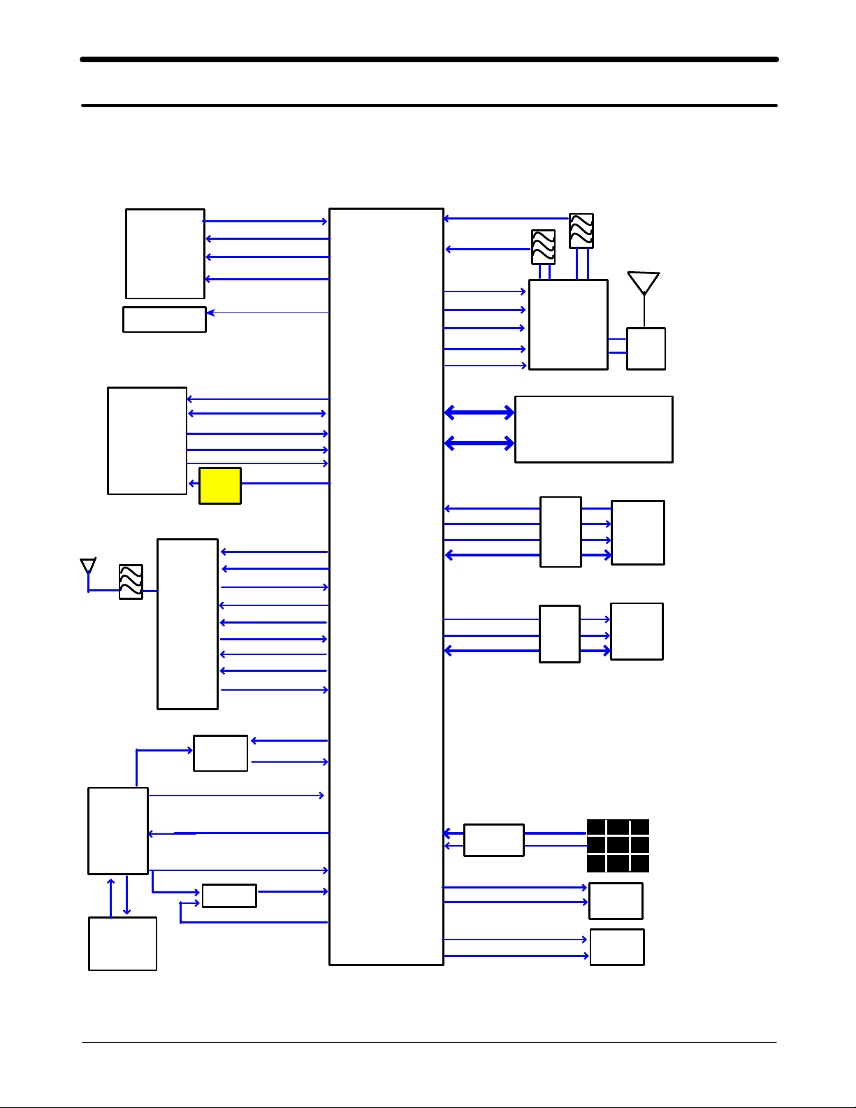
Block Diagram
8-1.
Repair
3
SAW
BT ANT
LCD Module
Back Light Driver
1.3M Camera
SAW
BT Module
Option
FLM,LCD RD
LCD_RS
LCD_DATA(0:7)
LCD_RST,RS,WR
EN_LCD_BL
CAM_SCL, RST
CAM_SDA
CAM_VSYNC HBYNC
CAM_DATA(0:7)
CAM_MCLK_OUT
CAM
EN_CAM_PWR
LDO
CLK26M_BT
BT_RST
BT_REQ_CLK
PCM_CLK
PCM_SYND
PCM_TXD
PCM_RXD
UART2_TXD
UART2_RXD
BASE Band
Catfish 118
PMB8808
DCS1800/PCS190_RX
GSM850/900_RX
BS1/BS2
TX_EN
VLOGIC
RAMP
HB / LB _TX
AD(0:15)
A(16:24)
DETECT_SD
SD_CMD
SD_CLK
SD_DATA(0:3)
SIM_RST
SIM_CLK
SIM_I/O
256M_NOR+128M_PSRAM
2G PAM
SWITCH
Module
MEMORY
SD
Socket
SIM
Socket
Main ANT
RF
SW
SD
CARD
SIM
CARD
FM_ANT
3.5 pi
Socket
EAR_PHONE
EAR_3.5
L/R
EAR_KEY
FM
LNA
COMP
EAR_ADC
FM_LNA_SW
FM_LNA_OUT
3.5_DETECT
EAR_SPK_L/R
RCV P
RCV N
SPK P
SPK N
Main Key
CON
Key_ROW(0:4)
ONKEY_N
RCV
SPK
8-1
SAMSUNG Proprietary-Contents may change without notice
This Document can not be used without Samsung's authorization
Page 2
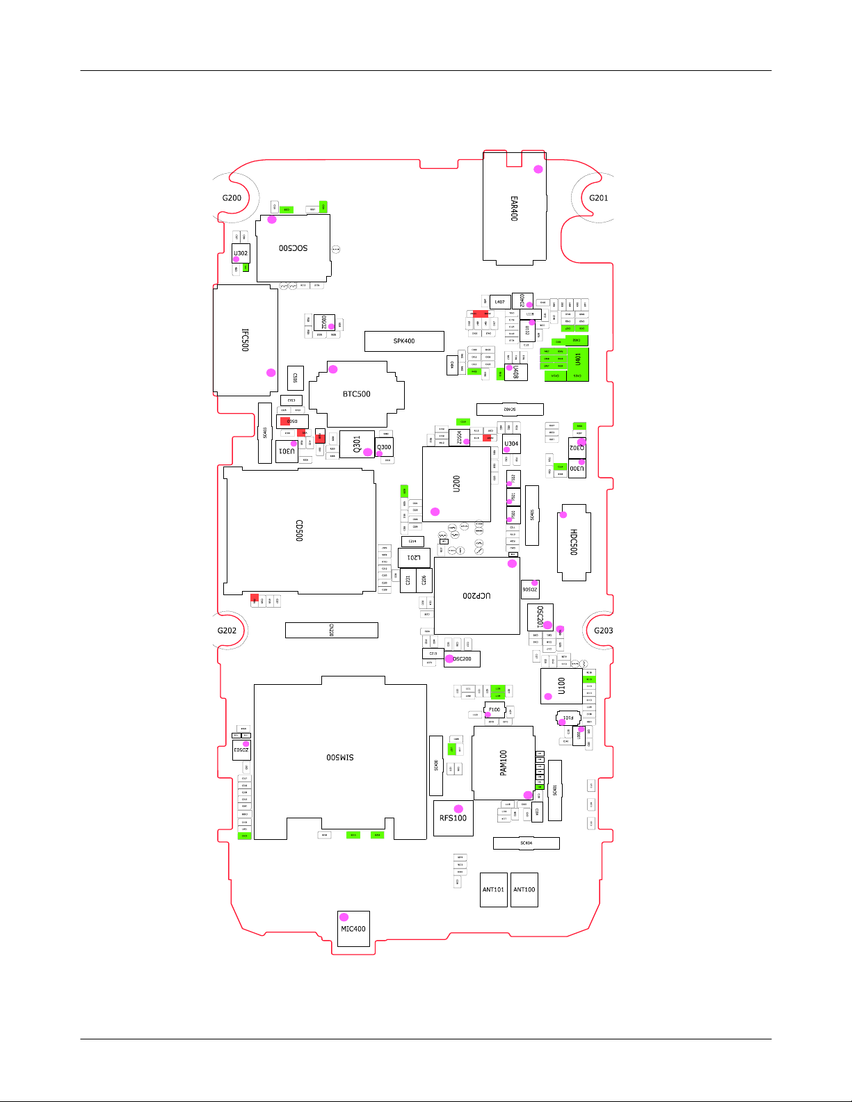
Level3Repair
PCB Diagrams
8-2.
8-2-1.
Top
8-2
SAMSUNG Proprietary-Contents may change without notice
This Document can not be used without Samsung's authorization
Page 3
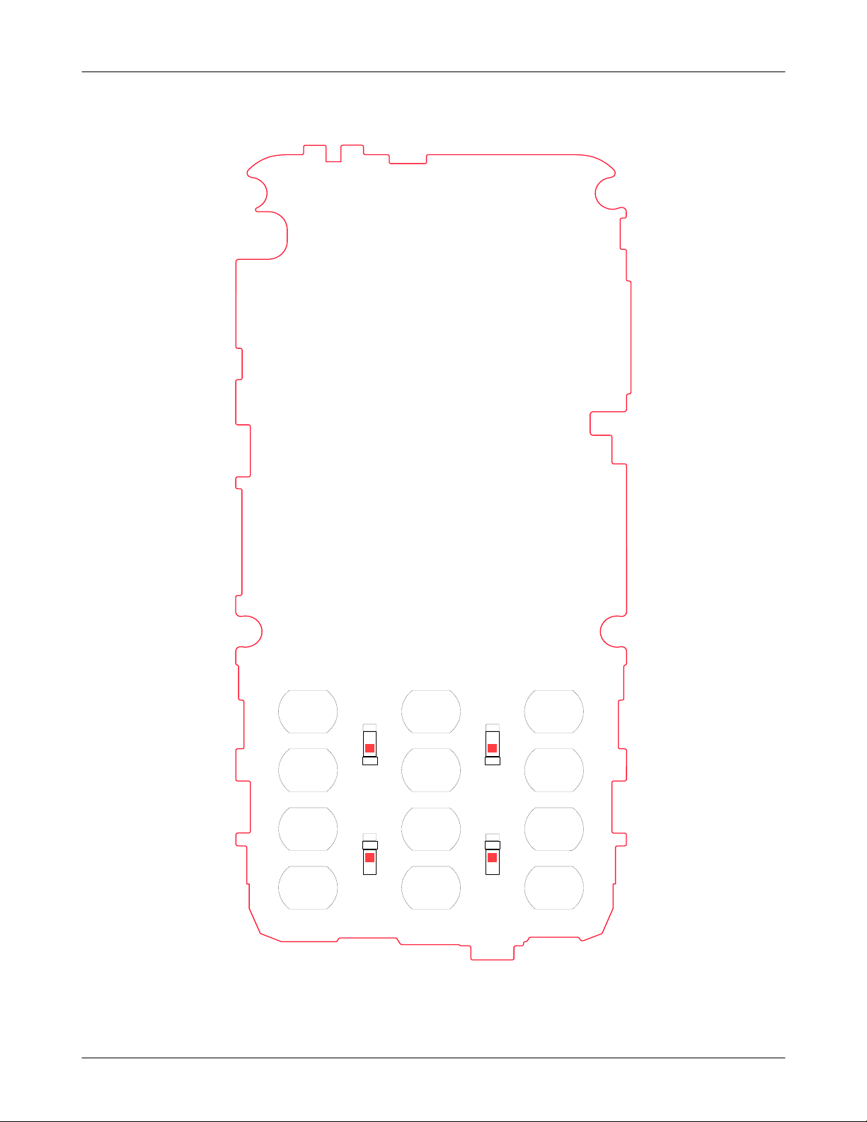
Level3Repair
8-2-1.
Bottom
ONE
R
N
STAR
L
E
D
5
0
1
2
5
R
F
O
U
V
S
E
E
2
1
2
C
5
2
5
R
1
0
0
5
D
E
L
E
EIGHT
O
F
I
V
R
Z
E
C522C523
L
E
D
5
0
3
R524
0
2
C
5
R
2
5
3
2
0
5
D
E
L
THREETWO
SIX
NINE
P
A
S
R
H
8-3
SAMSUNG Proprietary-Contents may change without notice
This Document can not be used without Samsung's authorization
Page 4

Level3Repair
8-2-3
SUB TOP
E
N
O
_
T
F
O
S
D
N
E
S
T
F
E
L
UP
OK
DOWN
T
H
G
I
R
O
W
T
_
T
F
O
S
D
N
E
8-4
SAMSUNG Proprietary-Contents may change without notice
This Document can not be used without Samsung's authorization
Page 5
Level3Repair
8-2-3
SUB BTM
8-5
SAMSUNG Proprietary-Contents may change without notice
This Document can not be used without Samsung's authorization
Page 6
Level3Repair
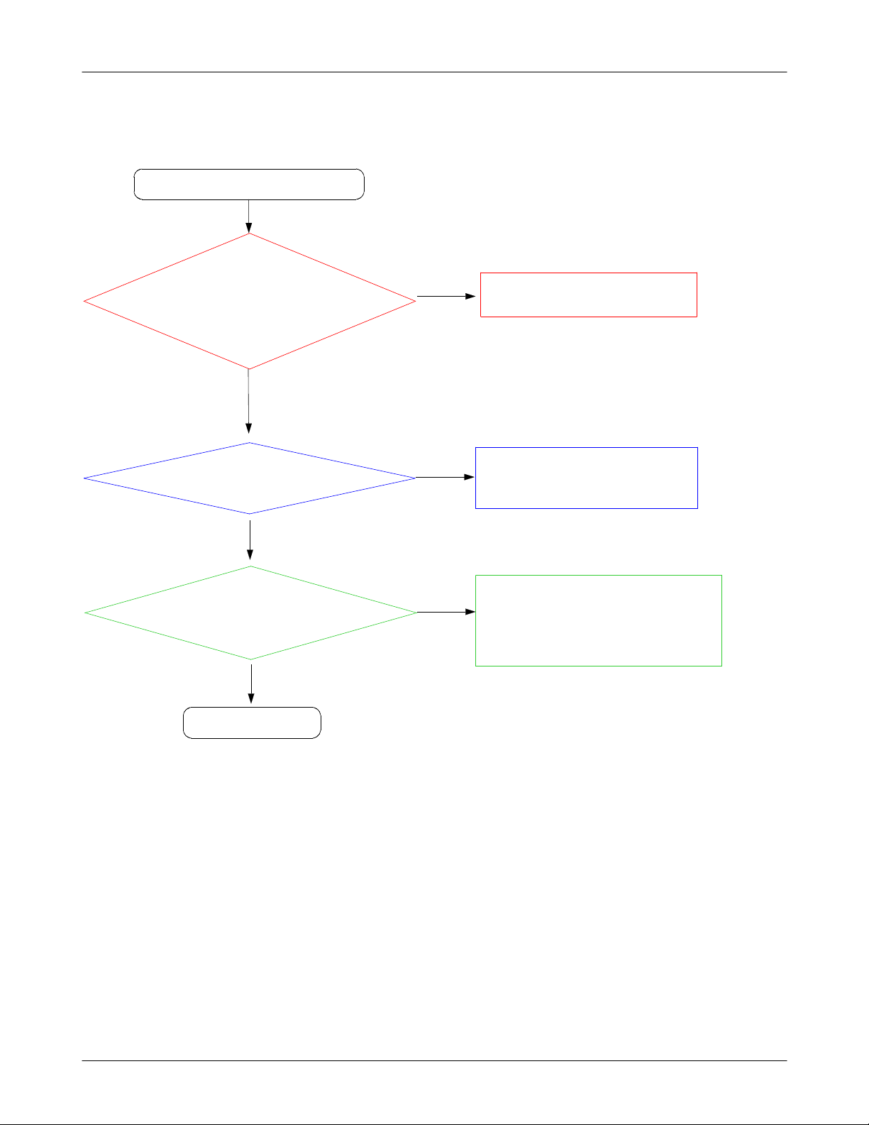
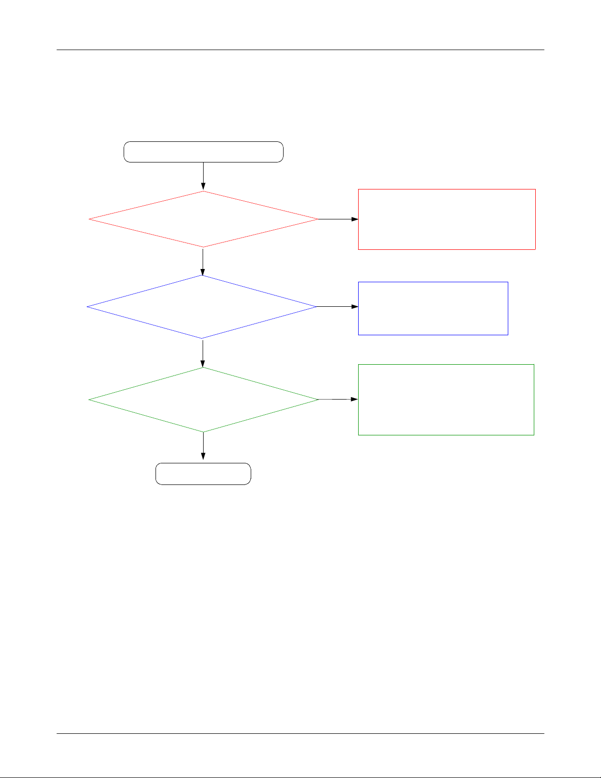
Flow Chart of Troubleshooting
8-3.
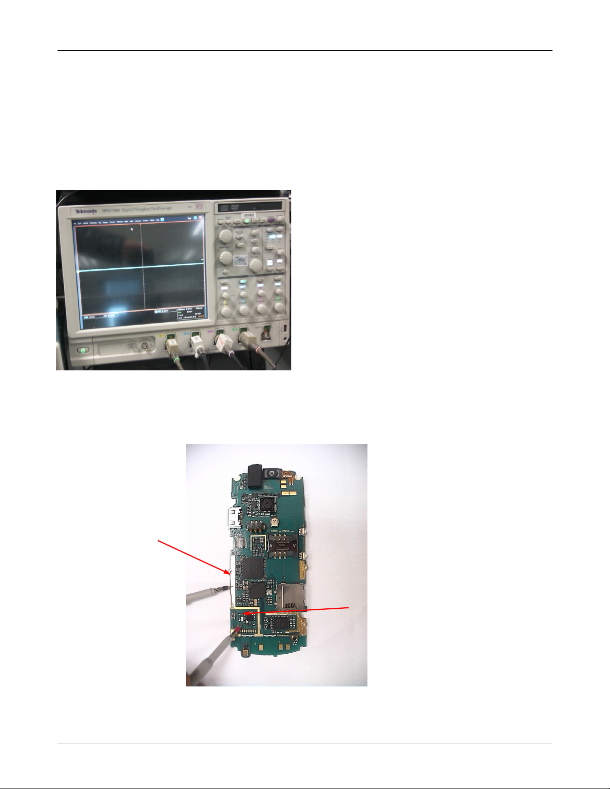
presetting methods for checking TP
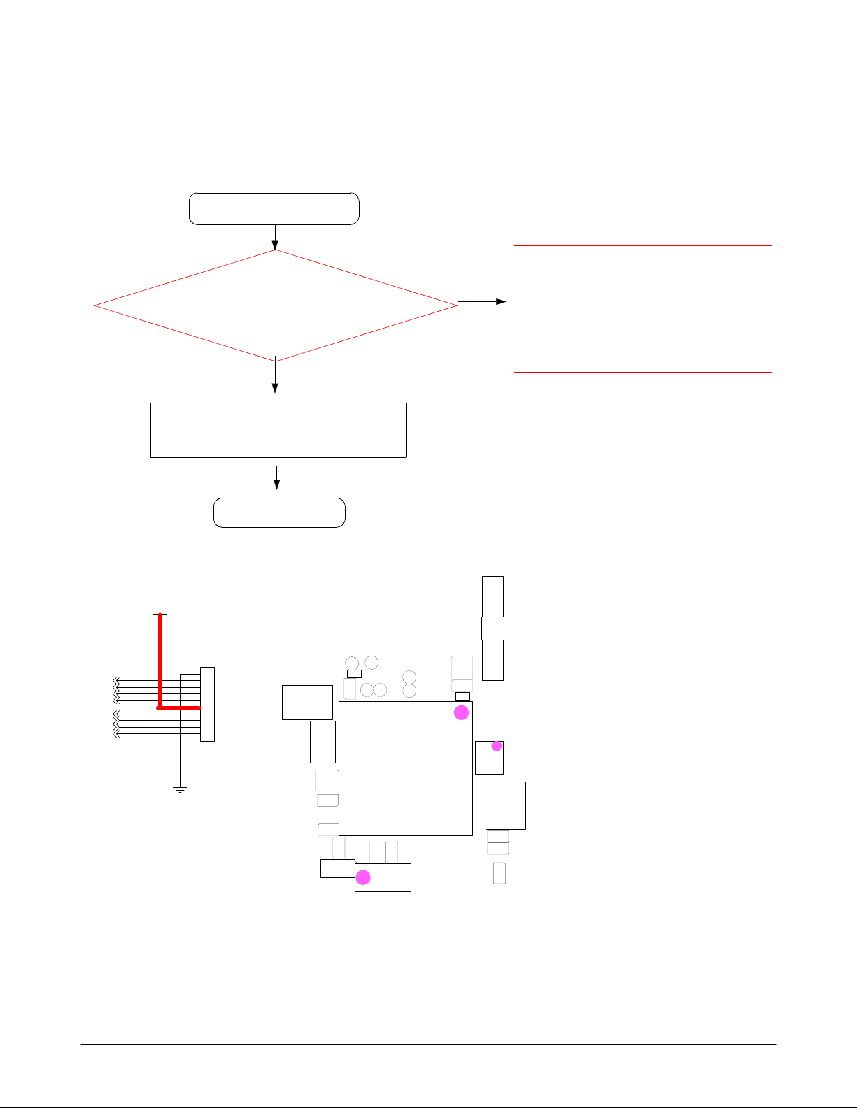
※
GND&TP(exp. VBAT=
-
look over the coming out signal.
-
C10
6, C220, C323
using Oscilloscope
)
GND
Oscilloscope
←
TP(Test Point)
8-6
SAMSUNG Proprietary-Contents may change without notice
This Document can not be used without Samsung's authorization
Page 7
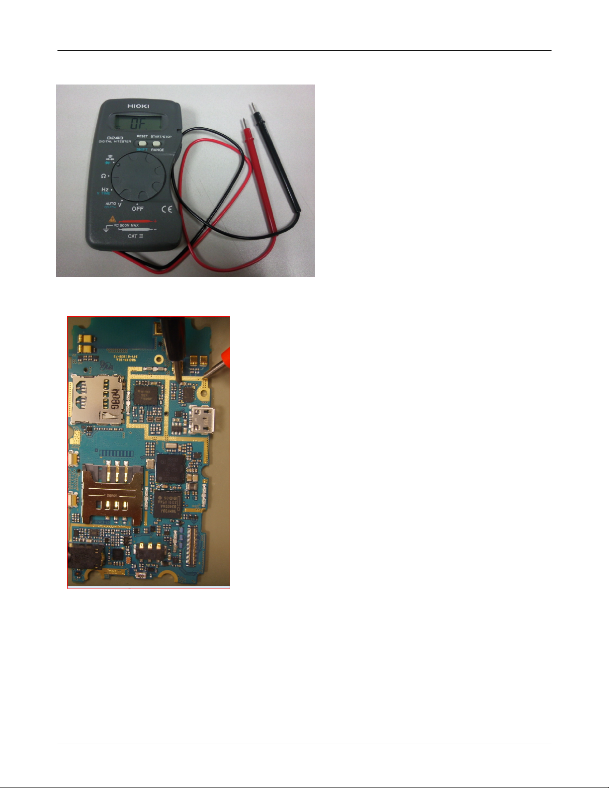
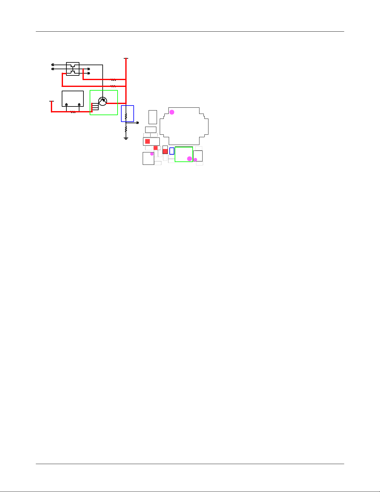
Multi-meter
←
Level3Repair
EX) to look up the TP, shunt Cap.
-
SAMSUNG Proprietary-Contents may change without notice
This Document can not be used without Samsung's authorization
Checking the TP(test point) using Multi-meter
←
if checking the GND, you can listen"beep"
-
if checking the Signal, you can't listen it.
8-7
Page 8
Level3Repair
8-3-1.
Power On
Power On'does not work
'
Check the Battery Voltage
is more than
TP:
(
C525 C513 C512
VDD_1.8V
(
Yes
Yes
=1.8
TP: C205)
3.7V
V?
No
No
Change the Battery
Because of batt. power low)
(
Check the Main Chip related to
SD1_FB=1.8V(TP:C231)
to lookover the Chip damage)
(
Yes
Check the Clock at
UCP200 A11pin
CLK26M)
(
TP:OSC201
(
END
=26M
1,3
Yes
HZ
pin
Check the Main Chip
to lookover the Chip damage)
No
)
(
OSC201
(TP:
using the oscilloscope)
pin/look over the
1,3
waverform
8-8
SAMSUNG Proprietary-Contents may change without notice
This Document can not be used without Samsung's authorization
Page 9
Level3Repair
BTC500
1
1
2
2
3
3
4
NC
5
NC
6
NC
7
NC
BATT.CON
LEDDRV
USE AS GPO
LEDFBN
LEDFBP
SENSEN
SENSEP
FE1
FE2
FMRIN
FMRINX
FSYS1
FSYS2
FSYS_EN
HSL
HSR
XO
XOX
ONOFF
SD1SW
0.3T
SD1_FB
ROUTE FROM C236(0.1T)
ADV_N
RD_N
RESET_N
TRST_N
WAIT_N
WR_N
TRIG_IN
T2IN
VBAT
0
0
5
D
1
0
5
V
USIF2_TXD_MTSR
L8
K10
L6
M6
B16
A14
M10
M11
G11
F11
K15
R14
T14
A11
B11
R9
R7
T6
R3
J1
L13
H15
J6
R4
K16
B4
C13
C
5
0
UART2_TXD
C227
C228
3
0
4
C
S
VDD_1.8V
5
1
2
5
C525
0
0
C300
1
3
0
C231
CLOSE TO THE PIN
C
3
1
5
C
D
5
1
R
5
2
0
U
5
0
BTC500
V50
V
5
0
0
8
0
3
R
4
1
5
C
0
R309
0
5
L
R306
3
R
6
3
2
C
R300
1
0
3
Q300
Q
3
2
0
R
C214
L
0
2
1
1
3
2
C
T
P
_
C
7
S
_
1
F
l
a
s
2
TP_WAITn
h
_
R
R
O
M
6
0
2
C
C
2
2
3
3
4
2
C
C
2
5
3
C224
6
4
1
0
2
2
C
C
C215
0
0
C
C
2
2
5
1
2
2
3
6
2
C
TP_WEn
TP_MEM_CLK
2
C
3
7
R510
4
0
2
R
T
P
_
n
D
R
C503
S
F
D
D
V
_
P
5
T
2
R
0
9
Z
0
D
6
C
P
U
5
O
S
C
2
0
1
C
2
0
0
1
0
C
2
C
2
8
1
C
2
2
0
7
1
C
2
C
1
2
7
C512
C513
C525
R520
VF
C514
EN_MAIN_KEY
L9
SENSE_N
SENSE_P
L200
BS1
BS2
ISOLATE
CLK26M_BT
BT_REQ_CLK
EAR_SPK_L
EAR_SPK_R
L201
ONKEY
ADVn
RDn
WAITn
WEn
NOISY
VDD_IO1_1.8V
RST_BB_J
R208
RST_BB
TRSTn
3.5_DETECT
R209
PMB8808
L8
LEDFBN
K10
LEDFBP
L6
SENSEN
M6
SENSEP
B16
FE1
A14
FE2
M10
FMRIN
M11
FMRINX
G11
FSYS1
F11
FSYS2
K15
FSYS_EN
R14
HSL
T14
HSR
A11
XO
B11
XOX
R9
ONOFF
R7
SD1SW
T6
SD1_FB
R3
ADV_N
J1
RD_N
L13
RESET_N
H15
TRST_N
J6
WAIT_N
CLK26M_BT
BT_REQ_CLK
EAR_SPK_L
EAR_SPK_R
ONKEY
ADVn
RDn
TRSTn
WAITn
SENSE_N
SENSE_P
BS1
BS2
ISOLATE
L200
RST_BB_J
RST_BB
NOISY
L201
VDD_IO1_1.8V
5
0
2
C
TP_WEn
TP_MEM_CLK
C
2
3
7
C214
7
1
2
TP_WAITn
R
L
0
2
1
6
3
2
C
6
1
0
3
2
2
C
C
C
2
2
3
3
4
2
C
5
2
C
3
C224
4
6
0
1
C
2
2
2
5
C
C
2
2
6
2
C227
FM_LNA_OUT
C
C215
OSC200
3
2
C
3
C228
CLOSE TO XO(SHIELD & CUT FILL)
OSC201
VDD_1.8V
21
3
C211
R
O
_
E
Z
D
A
_
P
T
R510
4
0
2
R
R
D
n
_
P
T
T
P
_
C503
C
S
_
S
F
l
F
a
s
h
D
_
D
R
O
V
M
_
P
R
T
5
0
9
0
0
2
P
C
U
C
2
1
3
H
D
C
5
0
0
Z
6
0
D
5
O
S
C
2
0
1
T
H
2
0
0
0
0
2
C
1
2
C
0
8
0
2
2
C
1
2
C
5
0
2
R
7
2
C
1
C
1
0
8
1
R
2
7
C
C
1
1
1
3
D
X
1
2
R
1
5
1
C
_
D
X
T
_
T
R
A
U
_
P
T
T
R
A
U
_
P
T
R116
R115
0
0
1
U
4
P
O
_
A
T
W
D
_
T
P
_
C
T
S
_
R
A
M
n
D
V
A
_
P
C208
T
C231
R208
CLOSE TO THE PIN
8-9
SAMSUNG Proprietary-Contents may change without notice
This Document can not be used without Samsung's authorization
Page 10
Level3Repair
8-3-2.
Initial
Initial Failure
Yes
CN200(RST_BB_J
using the oscilloscope GND
) > 1.7V?
SHORT PAD.
Yes
Check the16bit data signals.
Yes
END
&
ST_BB_J)must be higher than
R
No
Resolder UCP
200
1.7
V.
RST_BB_J
TRSTn
TXD1_J
RXD1_J
VDD_IO1_1.8V
CN200
4
0
2
C
3
2
1
1
2
TMS
TDI
TCK
TDO
2
3
3
4
4
5
5
6
6
7
7
8
8
9
9
10
10
7
7
1
2
TP_WAITn
R
6
0
2
C
C
2
3
4
3
5
2
C
C224
4
6
0
1
2
2
5
C
C
2
2
C
C215
_
R
T
P
D
n
T
P
_
C
S
_
S
F
l
F
a
s
D
h
_
D
R
V
O
_
M
P
T
P
2
0
0
C
C
C
2
2
2
1
6
3
R
C503
9
R
0
5
6
0
5
D
U
Z
0
2
C
0
2
2
C
0
8-10
SAMSUNG Proprietary-Contents may change without notice
This Document can not be used without Samsung's authorization
Page 11
Level3Repair
8-3-3.
Charging Part
Abnormal charging part
Yes
Check the Battery&TA
connection.
Yes
R304
> 4.9V?
Yes
No
No
be possible that it's not soldering well)
(
Reinsert the Battery or TA.
Resolder R304
Check the Q304 pin
>4.9V ?
Yes
END
4
No
Replace Q304 usingaHeatgun
8-11
SAMSUNG Proprietary-Contents may change without notice
This Document can not be used without Samsung's authorization
Page 12
Level3Repair
※
CS
PARALLEL FROM R310(0.1T)
VBAT
Q300
1
6
2
5
34
N
_
E
S
N
E
S
0.1,1%R306
TNHSVBSC
VDDCHG
P
_
E
S
N
E
S
1
2
5
6
1005
CHARGING CIRCUIT
Q301
VBUS_5V_OUT
R300
R302
3
4
VCHG
C
5
0
5
2
5
C
1
1
5
3
C
C525
0
0
5
D
1
0
C300
R
5
2
0
U
1
3
0
5
BTC500
5
V
V
5
0
0
8
0
3
R
4
1
5
C
0
R309
0
5
L
R306
0
3
R
R300
1
0
3
Q300
Q
2
0
3
R
R308
R309
8-12
SAMSUNG Proprietary-Contents may change without notice
This Document can not be used without Samsung's authorization
Page 13

Level3Repair
8-3-4.
Sim Part
Phone can't access SIM Card
Yes
SIM
pin1(C515)
500
After Power ON,
Check SIM_CLK Signal on
pin3(C517)of SIM
method:wiring pin3and
(
checking its waveform using an
second
≒
Yes
500ina
s.
2.85V
few
No
No
Resolder C515 R519 V502
insert SIM card&access it,
then must be sim pin1 or C515
Resolder or Replace SIM500 connector.
Because of not soldering well)
(
> 2.84V
Yes
After SIM card insert,
SIM
method:wiring pin3and check
(
pin2(R518, SIM_RST)
500
its waveform using an
Check the SIM Card
look over if it get damaged.)
(
2.85V?
≒
oscilloscope)
Yes
Yes
END
No
Confirm an another PBA
8-13
SAMSUNG Proprietary-Contents may change without notice
This Document can not be used without Samsung's authorization
Page 14

Level3Repair
VSIM_2.85V
SIM_RST
SIM_CLK
SIM500
R518
11
22
3344
G
10
C516
C517
C515 C518
SIM CON
R519
6
6
5
5
G
7GG89
2
0
5
V
SIM_IO
G202
C
C
2
5
9
2
0
1
1
0
7
8
5
5
R
V
C
N
2
0
0
R
1
5
8
R
5
0
8
R507
0
D
5
3
Z
1
0
5
C
C517
C516
C209
C515
L
0
4
0
C
9
4
0
C410
L401
C413
0
0
5
I
M
S
R214R215R216
C
2
2
3
3
4
2
C
3
2
C
5
C224
4
6
0
1
2
C
C
C
2
2
2
5
C
1
2
2
3
6
2
C
C215
OSC200
C
3
2
3
L111
2
1
5
2
2
0
1
1
1
L
L
L
L109
L123
C106
L
L
1
1
0
1
7
0
0
0
4
C
1
1
C
0
0
1
1
S
L
RFS100
L
2
1
6
1
L
5
2
8-14
SAMSUNG Proprietary-Contents may change without notice
This Document can not be used without Samsung's authorization
Page 15

Level3Repair
8-3-5.
Microphone Part
▶ Main MIC
Microphone does not work
MIC hall wil be Checked
blocked up by MIC rubber or
C406, L400
at MIC Active?
C406's on one side, it will
(
Yes
others
OK
be0V)
Not OK
2.2V
≒
No
MIC rubber set correctly or
Clean the MIC hall.
Replace UCP200 usingaHeatgun
Because of not soldering well
(
)
Yes
Check the status of soldering
(
L400, L401
ex. Crack)
(
OK
Check the MIC sample.
MIC400)
it be possible the problem)
(
OK
END
NotOK
NotOK
Resolder L400,
not work if those is not connected.)
(
Replace an another MIC(MIC400)
because of being possible the problem)
(
401
8-15
SAMSUNG Proprietary-Contents may change without notice
This Document can not be used without Samsung's authorization
Page 16

Level3Repair
MIC400
OUT
GND
GND
PWR
GND
GND
V_MIC_2.2V
0
0
4
L
1
2
3
4
5
6
C409
MAIN MIC
C413
L401
V_EARMIC
R400
C404
R401
R403
C400
EAR_MIC_PAUX_MIC_P
C410
MIC_MAIN_P
MIC_MAIN_N
AUX_MIC_N
PARALLEL
C403
C406
C411
C412
R405
EAR MIC
8
1
5
R
5
R
0
8
R507
0
3
Z
D
5
1
0
5
C
C517
C516
C209
C515
L
0
0
4
9
0
4
C
C410
L401
C413
I
M
S
5
0
0
0
0
4
C
S
RFS100
R214R215R216
MIC400
8-16
SAMSUNG Proprietary-Contents may change without notice
This Document can not be used without Samsung's authorization
Page 17

Level3Repair
8-3-5
Microphone Part
▶ Earphone MIC
Earphone MIC does not work
Yes
Check EAR400(Earjack) status
ex. bent metal, it will be not
(
contact earphone)
OK
C210 and R400
V?
2.2
≒
Not OK
No
Replace EAR400 usingaHeatgun
Caution, Plastic Mold is easy to melt.
(
Replace UCP200 usingaHeatgun
Because of not soldering well
(
)
)
Yes
Check the status of soldering
R400, R401, R403, C406,
C412, L402
ex. Crack)
(
OK
END
Not OK
Resolder R400, R401, R403, C406,
not work if those is not connected.)
(
C412, L402
8-17
SAMSUNG Proprietary-Contents may change without notice
This Document can not be used without Samsung's authorization
Page 18

Level3Repair
EAR400
IJAN4-120
C421
SEND_END
EAR_MIC_P
FM_ANT
EAR_L_3.5
EAR_R_3.5
3.5_CON_DETECT
V_EARMIC
2
CON-A
3
CON-B
6
CON-E
7
CON-F
5
CON-D
4
CON-C
5
6
L402
L403
L404
3
1
4
ZD400
2
R409
R410
C422
C426
C427C424
324C524C
L407
R400
3.5pi EARJACK
C404
C403
C406
R401
R403
C400
EAR_MIC_PAUX_MIC_P
C411
E
A
R
4
0
0
G201
AUX_MIC_N
PARALLEL
C412
R405
EAR MIC
0
L
0
4
0
2
4
L407
D
Z
C
4
1
2
0
4
Z
D
2
ZD401
8
8
5
1
0
0
4
4
4
L
L
C
C416
C400
R403
R
4
0
1
C406
C412
C411
C403
R
4
0
0
R405
4
1
4
R
L118
C119
7
1
4
C
U
C125
1
0
2
4
C
5
1
R113
R
1
0
1
C122
R
1
4
2
1
1
1
4
4
7
R
R
U
4
0
R
4
1
8
6
C
C
L
L
L
C420
1
3
6
9
0
1
R
4
4
4
4
4
0
0
0
2
2
3
4
6
4
5
R
4
9
0
1
4
R
0
5
3
1
3
1
C
4
R
2
3
2
2
C
4
4
C
C
2
4
C
C
7
4
2
6
C
4
0
2
C401
R
4
8
0
R407
1
0
C408
R418
4
U
C407
R404
4
1
5
4
4
0
C
C
8-18
SAMSUNG Proprietary-Contents may change without notice
This Document can not be used without Samsung's authorization
Page 19

Level3Repair
8-3-6.
Speaker Part
Speaker does not work
Wiring the SPK_N/P and
(
checking an waveform using
Yes
On MP3 playing,
L408, L405
oscilloscope)
Check the status of
soldering L405, L408
>2.0V
Yes
ex. Crack)
(
No
NotOK
Replace UCP200 usingaHeatgun
be possible of being UCPabad sample)
(
Resolder L405&L408
be possible because of soldering not well)
(
OK
Is Speaker working?
Listening through the
(
speaker)
Yes
END
No
Change Speaker
be possible of SPK Problems)
(
8-19
SAMSUNG Proprietary-Contents may change without notice
This Document can not be used without Samsung's authorization
Page 20

Level3Repair
SPK_P
SPK_N
L408
L405
C415
C416 C418
SPK CONTACT
R
5
2
8
0
R
0
5
2
5
9
D
Z
R
5
0
6
0
5
5
R
R
5
3
0
C
5
0
5
C417
SPK400
SPK400
2
1
0
0
4
4
D
D
Z
Z
L
4
0
2
2
4
Z
0
D
ZD401
8
5
8
1
0
0
4
4
4
L
L
C
4
1
5
C
C416
R403
C400
R
4
0
1
C406
C412
C
4
0
C411
4
C403
R
4
0
0
R405
4
1
4
R
L407
7
1
4
C
0
0
4
D
Z
4
2
1
C
C119
U
C125
1
0
2
R113
1
1
0
R
C122
R
4
1
2
1
7
1
1
4
4
R
R
U
4
0
R
8
4
1
6
BTC500
8-20
SAMSUNG Proprietary-Contents may change without notice
This Document can not be used without Samsung's authorization
Page 21

Level3Repair
8-3-7.
Receiver Part
See the sub circuit schematic.
-
Receiver does not work
On Voice calling,
check the voice signal at
L101(p), L102(n) using
Check the status of soldering
Yes
oscilloscope.
OK
L101, L102,
ex. Crack)
(
NotOK
NotOK
Replace UCP200 usingaHeatgun
Because of not soldering well
(
Resolder L101, L102,
not work if those is not connected.)
(
)
OK
Is Receiver working?
Listening through the
(
speaker)
Yes
END
No
Change Receiver
be possible of RCV Problems)
(
8-21
SAMSUNG Proprietary-Contents may change without notice
This Document can not be used without Samsung's authorization
Page 22

Level3Repair
presetting
※
Rx setting)
(
Active Cell
1.
select GSM or GPRS
:
Connetion Type
2.
select Auto(GSM), BLER(GPRS)
:
BCH Parameter
3.
select measuring band(DCS or EGSM)
:
Cell power
4.
dBm
:-60
8960
Tx setting)
(
8-22
SAMSUNG Proprietary-Contents may change without notice
This Document can not be used without Samsung's authorization
Page 23

Level3Repair
After setting
※
After setting, prepare the call setup Display
1.
UsinganOriginateCall,makeacall.
2.
Confirm the display"connected"
3.
start the measuring
4.
8960 &
※
8960 (
spectrum analyzer
EGSM/DCS
)
down&up at picture)
(
spectrum analyzer:testing method=the way using an Osciliscope
-
-8960:
connect using RF Cable between
SAMSUNG Proprietary-Contents may change without notice
This Document can not be used without Samsung's authorization
8960 &
RF Connector in board.
8-23
Page 24

Level3Repair
RF Connector
8-24
SAMSUNG Proprietary-Contents may change without notice
This Document can not be used without Samsung's authorization
Page 25

Level3Repair
8-3-10.
GSM
Cell Power
PAM100
(
spectrum analyzer)
PAM100 Pin12
(
specturm analyzer)
Receiver
850
RX ON
:-60
Yes
Pin
dBm
-65
TP:L110 using
Yes
dBm
-68
TP:C133 using
Yes
17
dBm
≥
≥
No
No
Resolder PAM100, L110,C101,
L101
Check PAM100
pin
4=L,
pin6=H
pin
=
5
L,
No
Yes
Check ANT Switch
control circuit
Resolder PAM100
TCXO CLOCK CHECK?
MHz@OSC201
26
Yes
Check UCP20
END
0
Yes
No
Resolder OSC201
8-25
SAMSUNG Proprietary-Contents may change without notice
This Document can not be used without Samsung's authorization
Page 26

Level3Repair
8-3-11.
GSM
Cell Power
PAM100
(
spectrum analyzer)
PAM100 Pin13
(
specturm analyzer)
Receiver
900
RX ON
:-60
Yes
Pin
dBm
-65
TP:L110 using
Yes
dBm
-68
TP:C132 using
Yes
17
dBm
≥
≥
No
No
Resolder PAM100, L110,C101,
L101
Check PAM100
pin
4=L,
pin6=H
pin
5
=H,
No
Yes
Check ANT Switch
control circuit
Resolder PAM100
TCXO CLOCK CHECK?
MHz@OSC201
26
Yes
Check UCP20
END
0
Yes
No
Resolder OSC201
8-26
SAMSUNG Proprietary-Contents may change without notice
This Document can not be used without Samsung's authorization
Page 27

Level3Repair
8-3-12.
DCS Receiver
RX ON
Cell Power
PAM100
(
spectrum analyzer)
PAM100 Pin12
(
specturm analyzer)
TCXO CLOCK
MHz@OSC201
26
:-60
Yes
Pin
17
dBm
-65
TP:L110 using
Yes
dBm
-68
TP:C133 using
Yes
CHECK?
dBm
≥
≥
No
No
No
Resolder PAM100, L110,C101,
L101
Check PAM100
pin
Resolder OSC201
4=L,
pin6=H
pin5=L,
No
Yes
Check ANT Switch
control circuit
Resolder PAM100
Yes
Check UCP20
Yes
END
0
8-27
SAMSUNG Proprietary-Contents may change without notice
This Document can not be used without Samsung's authorization
Page 28

Level3Repair
8-3-13.
PCS Receiver
RX ON
Cell Power
PAM100
(
spectrum analyzer)
PAM100 Pin13
(
specturm analyzer)
TCXO CLOCK
MHz@OSC201
26
:-60
Yes
Pin
17
dBm
-65
TP:L110 using
Yes
dBm
-68
TP:C132 using
Yes
CHECK?
dBm
≥
≥
No
No
No
Resolder PAM100, L110,C101,
L101
Check PAM100
pin
Resolder OSC201
4=L,
pin6=H
pin5=H,
No
Yes
Check ANT Switch
control circuit
Resolder PAM100
Yes
Check UCP20
Yes
END
0
8-28
SAMSUNG Proprietary-Contents may change without notice
This Document can not be used without Samsung's authorization
Page 29

Level3Repair
ANT100
ANT101
C100
C139
RFS100
G
G
C
A
4
2
1
3
L125
L126
C101
L101 L107
RF
L110
VBAT
C103
C104
C105
C138
C106
R117
0
7
3
1
T
T
N
VLOGIC
RAMP
TX_EN
LB_TX GSM900_PCS1900_RX
L114
HB_TX
R101
R103
R105
L115
L116
C108
2
VLOGIC
3
VRAMP
4
TX_EN
27
GSM_IN
29
DCS|PCS_IN
G
1
7
C109
TP_MEM_CLK
7
3
C
2
C214
7
1
2
TP_WAITn
R
0
L
1
2
6
3
2
C
6
1
0
3
2
2
C
C
C
2
2
3
3
4
2
C
5
C
3
2
C224
4
6
0
1
2
2
5
C
C
2
2
C
C215
OSC200
3
C
3
2
C106
L
1
0
7
0
0
4
1
C
0
1
S
L
RFS100
T
A
A
B
V
PAM100
G
G
G
G
G
G
G
G
G
G
G
G
0
6
9
5
8
0
2
1
3
4
1
1
1
1
1
2
2
9
8
2
2
2
T
n
_
D
P
R
T
P
_
C
S
_
S
F
F
l
a
s
D
h
D
_
R
V
O
_
M
P
T
0
0
P
C
U
2
C
C
2
2
1
2
3
6
L106
L111
5
1
2
0
2
2
1
1
1
L
L
L
L104
L109
F100
L123
3
3
2
1
C
3
1
L
1
1
0
C
1
0
1
0
0
1
M
A
P
L115
L116
4
1
1
L
5
BS1
R102
6
BS2
R118
12
RX1
13
RX2
11
G
14
G
G
G
G
G
G
G
G
G
G
G
4
3
2
5
6
6
5
8
1
3
3
3
3
3
2
2
2
3
4
R
0
2
C503
9
0
R
5
6
0
5
Z
D
O
S
C
2
0
1
T
H
2
0
0
0
0
1
0
C
2
C
2
2
C
0
2
8
C
1
2
5
0
2
R
7
C
1
2
C
1
8
R
0
1
2
7
C
C
1
1
1
3
2
1
5
C
1
1
D
X
T
_
T
R
A
_
U
P
T
0
0
0
0
1
L
4
2
1
L
C
8
0
1
C
1
U
1
0
1
F
0
2
1
C
3
0
3
U
C140
R117
R118
R102
0
R
1
5
R
1
3
0
C
1
9
0
0
R
1
1
1
0
4
C
C
1
S
3
8
C105
C
1
0
C
4
1
0
3
BS1
BS2
GSM850_DCS1800_RX
G203
D
X
R
_
T
R
A
U
_
P
T
R116
R115
1
C
1
1
4
C
1
1
3
C
1
1
L120
C130
0
0
3
L
C
3
0
1
5
0
3
C
1
2
1
C
4
3
1
C
3
2
1
C
SC404
PMB8808
USE AS GPO
ROUTE FROM C236(0.1T)
DIRTY GND : E12,F12,G12 (TO C207,C224,C225,C241)
CLEAN GND : C15,F14,F15,F13 (TO C204,C205,C208,C209,C221)
T7 CONNECT TO
ONLY C219,C238
U
1
B
D
M
I
O
S
P
V
_
_
_
X
1
2
4
3
S
S
S
S
C
C
C
C
S
S
S
S
N
V
V
N
N
V
N
V
6
6
8
1
7
9
1
1
1
T
T
T
A
R
T
A
1
0.3T
C
N
2
USIF1_RXD_MRST
USIF1_TXD_MTSR
USIF2_RXD_MRST
USIF2_TXD_MTSR
C
N
USIF1_CTS_N
USIF1_RTS_N
USIF2_CTS_N
USIF2_RTS_N
LEDDRV
LEDFBN
LEDFBP
SENSEN
SENSEP
FE1
FE2
FMRIN
FMRINX
FSYS1
FSYS2
FSYS_EN
HSL
HSR
XO
XOX
ONOFF
SD1SW
SD1_FB
ADV_N
RD_N
RESET_N
TRST_N
WAIT_N
WR_N
TRIG_IN
T2IN
PABIAS
PABS
PAEN
ACD
ANAMON
VDD_FMR
VDET
VIB
VPMU
VRAMP
VREF
VRF1
VRTC
VSHNT
B2
A3
J8
H7
B3
A2
J7
H8
L9
L8
K10
L6
M6
B16
A14
M10
M11
G11
F11
K15
R14
T14
A11
B11
R9
R7
T6
R3
J1
L13
H15
J6
R4
K16
B4
C13
B13
C12
R10
P9
N11
C14
T8
P10
A13
T10
H10
L10
K6
DON’T CONNECT H10 & J10
IN SAME LAYER
CLK26M_BT
BT_REQ_CLK
EAR_SPK_L
EAR_SPK_R
ONKEY
ADVn
RDn
TRSTn
WAITn
WEn
CLOSE TO THE PIN
VF
EN_CAM_PWR
EN_EAR_AMP
UART1_RXD
UART1_TXD
UART2_RXD
UART2_TXD
EN_MAIN_KEY
SENSE_N
SENSE_P
BS1
BS2
ISOLATE
3.5_DETECT
VLOGIC
TX_EN
SEND_END_DIRECT
MOT_EN
RAMP
VSHNT
C234
L200
RST_BB_J
RST_BB
NOISY
C235
VDD_IO1_1.8V
C227
VDD_1.8V
C231
FM_LNA_OUT
CLOSE TO XO(SHIELD & CUT FILL)
OSC201
21
3
CLOSE TO THE PIN
4
C228
L201
R208
R209
VRTC_2.3V
VDD_1.8V
C236
C233C232
8-29
SAMSUNG Proprietary-Contents may change without notice
This Document can not be used without Samsung's authorization
Page 30

Level3Repair
8-3-14.
GSM
GSM900 Transmitter
850/
TX Power is too Low!!
TX ON(5Level)
TCXO CLOCK CHECK?
26
PAM100 pin
Check the Voltage
MHz@OSC201
YES
27≥-4
dBm
YES
C104
<3.3
V?
NO
NO
NO
solder OSC201
Re-
solder or change
Re-
UCP200
Check the UCP200&VBAT
circuit.
YES
PAM100
(
Pin
17
dBm
30
TP:L110 using
≥
spectrum analyzer)
YES
Check the RFS100
connection with PCB?
YES
Antenna
re-solder or change
NO
Resolder PAM100
NO
Resolder RFS100.
8-30
SAMSUNG Proprietary-Contents may change without notice
This Document can not be used without Samsung's authorization
Page 31

Level3Repair
8-3-15.
DCS/PCS Transmitter
TX Power is too Low!!
TX ON(5Level)
TCXO CLOCK CHECK?
26
PAM100 pin
(
spectrum analyzer)
Check the Voltage
MHz@OSC201
YES
29≥-4
dBm
TP:L115 using
YES
C104
<3.3
V?
NO
NO
NO
solder OSC201
Re-
solder or change
Re-
UCP200
Check the UCP200&VBAT
circuit.
YES
PAM100
(
Pin
17
dBm
30
TP:L110 using
≥
spectrum analyzer)
YES
Check the RFS100
connection with PCB?
YES
Antenna
re-solder or change
NO
Resolder PAM100
NO
Resolder RFS100.
8-31
SAMSUNG Proprietary-Contents may change without notice
This Document can not be used without Samsung's authorization
Page 32

Level3Repair
X
L125
RFS100
G
G
4
3
C
A
2
1
L101 L107
C101
RF
L110
C105
C138
C103
VBAT
C104
ANT101
C139
C100
L126
C106
R117
0
7
3
1
T
T
T
VLOGIC
RAMP
TX_EN
LB_TX GSM900_PCS1900_RX
HB_TX
L114
R101
R103
R105
L115
L116
C108
2
C
5
1
5
3
1
C525
0
5
0
D
3
0
4
C300
C
S
U
3
0
1
C
D
5
0
0
C
C
2
5
9
2
0
1
1
0
7
8
5
5
R
V
G202 G203
5
8
R
1
8
0
5
R
R507
BTC500
C
V
5
1
0
V
5
0
0
8
0
3
R
R
5
4
2
1
0
5
C
0
R309
0
5
L
R306
3
5
R
0
C
N
2
0
0
R300
1
0
3
Q300
Q
3
2
R
0
0
2
7
R
6
0
2
R
1
2
0
C
C212
6
3
C203
2
C
C230
C229
2
VLOGIC
3
VRAMP
4
TX_EN
27
GSM_IN
29
DCS|PCS_IN
G
G
8
7
1
C109
C219
1
5
4
R
R515
4
R
1
5
3
0
R
5
3
1
3
R
2
0
9
R
2
0
C221
8
C220
R
5
1
1
C506
C208
5
0
2
C
C214
L
0
2
1
6
1
0
3
2
2
C
C
C
2
2
3
3
4
2
C
2
5
C
3
C224
6
1
2
C
C215
2
3
3
R516
D
R512
Z
0
0
2
U
C
_
S
R
_
A
P
M
T
n
V
D
A
_
P
T
TP_WEn
TP_MEM_CLK
7
3
2
C
T
P
_
C
7
S
_
1
F
l
a
2
s
TP_WAITn
h
_
R
R
O
M
2
0
0
4
0
C
C
2
2
2
5
C
1
2
2
3
6
2
C
OSC200
C
L111
2
2
1
L
L109
L123
C106
N
A
A
B
V
PAM100
G
G
G
G
G
G
6
5
0
9
8
9
1
1
1
1
1
2
0
4
C
S
R
4
3
3
1
0
0
3
3
2
C
5
7
0
C
C
0
5
5
D
Z
U304
R
2
0
1
C
3
1
0
1
2
3
R
C
2
2
2
2
3
2
0
2
C
5
F
1
0
5
F
0
0
5
F
A
_
W
O
D
T
_
P
T
C211
P
A
E
T
_
D
Z
R
_
O
R510
0
2
4
R
n
D
_
R
P
T
C503
S
F
D
D
V
_
P
T
9
0
5
R
C
P
U
L106
0
5
1
0
0
2
1
1
1
L
L
L
L104
4
F100
2
1
L
2
3
3
3
1
C
1
C
G
G
G
G
G
G
G
G
G
G
G
5
4
2
3
8
1
0
2
6
1
2
2
5
0
4
C
S
6
5
D
0
Z
O
S
C
2
0
1
2
C
0
0
2
2
C
0
C
1
2
7
C
1
3
1
2
2
2
2
2
3
2
3
C227
R406
2
8
C
2
R307
L
2
0
0
3
Q
0
2
C
5
2
6
0
0
U
3
C524
C
5
0
4
R304
H
D
C
5
0
0
T
H
2
0
0
0
2
1
C
1
2
8
C
5
0
2
R
7
1
2
C
0
1
8
R
C
1
1
D
X
2
R
1
5
C
1
_
D
X
T
_
T
R
A
U
_
P
T
T
R
A
U
_
P
T
R116
R115
0
1
1
C
1
0
1
4
1
1
C
U
3
1
1
C
L120
C130
1
F
0
1
0
0
L
3
C
3
0
0
2
1
1
C
3
0
3
U
C140
5
BS1
BS2
RX1
RX2
G
G
G
G
G
G
3
5
4
6
3
3
3
3
R102
6
R118
12
13
11
14
BS1
BS2
GSM850_DCS1800_R
PAM
8-32
SAMSUNG Proprietary-Contents may change without notice
This Document can not be used without Samsung's authorization
Page 33

Camera
Level3Repair
Camera does not work
Yes
Check VGA Camera
connection(SOC500)
Yes
Check Camera supply
voltage @C306(VBAT)
, @C307(2.8V), C308(1.8V)
OK
Check the EN_CAM_PWR
signal @U302's pin 3,4
Yes
Change the Camera module
Yes
No
NotOK
No
Insert VGA CAM module
into SOC500 properly
Resolder U302 or Replace U302
Resolder R313 or Replace R313
END
8-33
SAMSUNG Proprietary-Contents may change without notice
This Document can not be used without Samsung's authorization
Page 34

Level3Repair
VCAM_A_2.8V
CAM_HSYNC
CAM_PCLK_IN
CAM_MCLK_OUT
CAM_VSYNC
CAM_O(4)
CAM_RST
CAM_SDA
CAM_SCL
CAM_O(7)
CAM_O(6)
CAM_O(5)
CAM_O(3)
CAM_O(2)
CAM_O(1)
CAM_O(0)
TP_CAM_HSYNC
TP_CAM_VSYNC
TP_CAM_RST
C508
VCAM_1.8V
VCAM_1.8V
VCAM_A_2.8V
R313
VBAT
C306
C309
U302
1
6VOUT1
VIN
2
5
GND
VOUT2
3
4
EN2
EN1
GND
7
C308
C307
6
0
5
L
C509
SOC500
1
1
2
2
3
3
4
4
5
5
6
6
7
7
8
8
9
9
10
10
11
12
13
14
15
16
17
18
19
20
21
22
23
C510
24
EN_CAM_PWR
11
12
13
14
15
16
17
18
19
20
GND
GND
GND
GND
VGA CAM SOCKET
CAM LDO
G200
U302
C
5
1
0
C
C
3
3
0
0
8
7
9
0
3
6
C
0
3
C
TP_CAM_HSYNC
I
F
C
5
0
0
C525
3
0
4
C
S
C
5
0
9
L
0
5
6
C
5
8
0
0
0
5
C
O
S
TP_CAM_RST
R
2
0
1
R211
TP_CAM_VSYNC
R
5
0
2
8
0
R
5
5
2
9
D
Z
R
5
0
6
0
3
5
5
R
R
5
0
C
5
0
5
1
2
5
C
5
C
3
1
0
0
D
5
1
C300
R
5
2
0
3
0
1
U
BTC500
V
5
0
V
5
0
0
8
0
3
R
4
1
5
C
0
R309
0
5
L
R306
R
3
0
5
SPK400
R300
1
0
3
Q300
Q
R
3
2
0
8-34
SAMSUNG Proprietary-Contents may change without notice
This Document can not be used without Samsung's authorization
Page 35

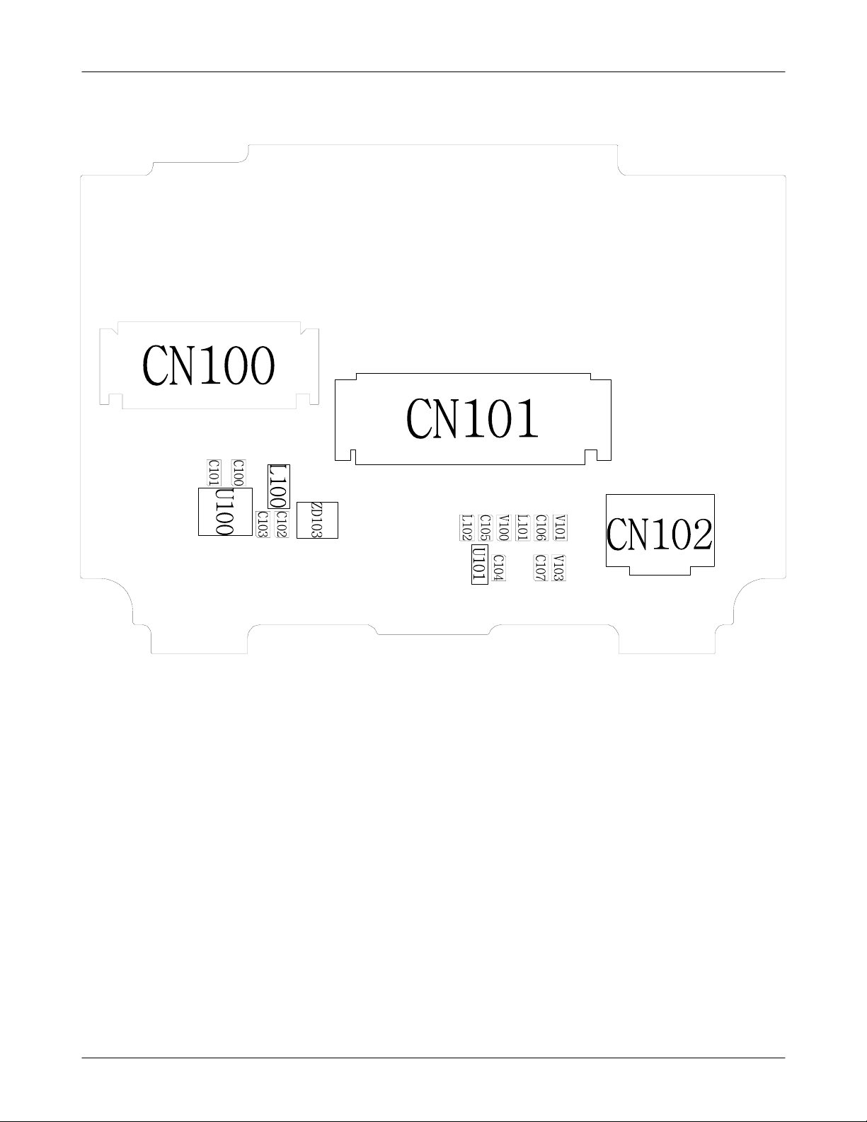
LCD
Level3Repair
LCD is not displayed
Yes
Check VBAT is
Check the voltage @U100's
LED_A > 2.7V
Is LCD displayed?
END
Yes
OK
Yes
3.4
V~4.1V
No
NotOK
No
check battery
Resolder U100 or L100
Replace LCD Module
8-35
SAMSUNG Proprietary-Contents may change without notice
This Document can not be used without Samsung's authorization
Page 36

Level3Repair
KEY_ROW(3)
KEY_ROW(4)
VDD_2.9V
AXT634124AW1
RCV_P
LCD_D1(0)
LCD_D1(2)
LCD_D1(4)
LCD_D1(6)
LCD_RS_O
LCD_WR_O
LCD_CS_O
LCD_RD
KEY_ROW(2)
ONKEY_N
C503
1000NF
6.3V
1005
11
55 66
7
788
99
11 11 12
13 14
13
15 16
15
171718
19
19
212122
232324
252526
27
27
293330
29
313132
333334
NCN C
35
Main LCD CON.
CN100
C
C
L
1
1
1
0
0
1
0
0
U
0
1
0
0
Z
D
C
C
1
1
1
0
0
0
3
2
3
HDC500
36NC37 38
VMOT_3.3V
2
2
44
1010
12
14
16
18
20
20
22
24
26
28
28
30
32
34
NC
CN101
VBAT
VDD_IO2_1.8V
RCV_N
EN_LCD_BL
LCD_D1(1)
LCD_D1(3)
LCD_D1(5)
LCD_D1(7)
FLM_O
LCD_RST
KEY_COL(1)
KEY_COL(2)
KEY_COL(3)
V
6
5
4
1
3
U
5
L
0
V
R510
C526
4.7K
1000nF
1005
10V
1005
C504
1000NF
6.3V
1005
5
D
S
E
P
6
0
5
D
Z
2
VBAT
L100
LED_A
U100
SUB
10
NC
9
8
GND
7
D1
6
D2D3
D
N
G
1
1
LCD_BL(1)
LCD_BL(2)LCD_BL(3)
EN_LCD_BL
1
NC
2
NC NC
3
IN
4
EN
5
C103
C
C
L
V
L
1
0
2
V
1
1
1
1
1
0
0
0
0
0
1
0
1
6
5
U
C
1
1
0
0
1
4
C
V
1
1
0
0
3
7
CN102
MAIN LCD DC/DC
.
8-36
SAMSUNG Proprietary-Contents may change without notice
This Document can not be used without Samsung's authorization
Page 37

Level3Repair
9-14.
Bluetooth part(GT-E2330B Only)
Bluetooth connection disable
Yes
Check BT function ON
Yes
Check power of U100,
VDD_1.8V
VBT_1.5V
Check pin A3 of
(26
MHz)
V,
1.8
≒
V?
1.5
≒
Yes
U100
No
Enable BT function
No
Resolder U100
No
Resolder C127
Yes
Check the assembled
F101,C120,C121,L120,C130,
status of
C140,C134,C123
Yes
END
No
Resolder error parts
8-37
SAMSUNG Proprietary-Contents may change without notice
This Document can not be used without Samsung's authorization
Page 38

Level3Repair
BT
BT_REQ_CLK
PCM_TXD
PCM_RXD
PCM_CLK
PCM_SYNC
UART2_RXD
UART2_TXD
C113
C114
TP_UART_RXD
TP_UART_TXD
C115
G4
G7
G6
R116
B4
AIO0
C4
PIO0
B5
PIO1
C5
PIO2
C6
PIO3
E7
PIO4
B7
PIO5
D5
PIO7
C7
PIO9
PCM_IN
H2
PCM_OUT
H3
PCM_CLK
H4
PCM_SYNC
SDIO_DATA0|CSPI_MISO|UART_TX
F6
SDIO_DATA1|CSPI_INT|UART_RTS
F7
SDIO_DATA2|UART_RX
SDIO_DATA3|CSPI_CS#|UART_CTS
H7
SDIO_CLKCSPI_CLK
D6
SDIO_CMDCSPI_MOSI
E5
SDIO_SD_CS#
E6
CLK_32K
R108
A
N
A
_
S
S
V
3
6
B
C
VDD_1.8V
7
1
7
D
A
A
E
S
A
R
D
N
A
O
A
_
P
C
_
_
D
D
D
D
D
V
D
V
V
U100
G
G
I
I
O
D
L
D
_
_
_
S
S
S
S
S
S
V
V
V
5
1
1
E
H
C
VDD_1.8VVBT_1.5V
GT-E2330 NC
GT-E2330B O
C131
C111
CLK26M_BT
VDD_1.8V
R115
F101
6
4
BT_RST
BAL
BAL
3
57G8
G
VBT_1.5V
GNC
UNBAL
DC
L120
C134 C123
C120
C121
1
2
C140
C130
1
6
H
G
S
O
I
D
D
A
A
P
R
_
_
D
D
D
D
V
V
SPI_MISO
SPI_MOSI
VREGIN_H
VREGIN_L
VREGOUT_H
VREGENABLE
XTAL_OUT
N
E
O
I
E
R
D
A
C
R
S
_
_
S
S
S
S
V
V
3
F
SPI_CLK
SPI_CS#
XTAL_IN
LO_REF
TEST_EN
C112
H1
E4
F4
G2
A5
B2
A4
A6
E2
RF_N
F2
RF_P
C127
A3
A2
G3
RST#
B3
G5
C2
N|CS
D2
N|CS
D4
N|CS
F5
N|CS
1
NC
2
NC
8-38
SAMSUNG Proprietary-Contents may change without notice
This Document can not be used without Samsung's authorization
Page 39

Service Schematics
8-4.
NC Point(Top View)
-
NC
:
U100
1234567
A
○○○●●○○
B
○○○●●○●
C
○●○●○●●
D
○●○
E
○○○●●●●
●
●○○
ㅅ
Level3Repair
F
○○○●●●○
G
○●○○●●○
H
●○○○○○○
U200
1234567891011121314
A
●●
B
C
D
E
F
G
H
●● ○○ ○●
○○○○○○○○○○
○○○○○○○○○○
○○○○○○○○○○
○○○○○○○○○○
●○ ○○ ○●
J
K
●●
8-39
SAMSUNG Proprietary-Contents may change without notice
This Document can not be used without Samsung's authorization
Page 40

Level3Repair
UCP200
12345678910111213141516
A
●○○○○○○○○○○○○○○●
B
○○○○○○○○○○○○○○○○
C
○○○○○○○○○○●○●●○○
D
○○○○●●●○○○●●●●●○
E
○●○●●○○○○○○○●●●○
F
○○○○●○○○○○●○○○○○
G
○○○○○○○○○○○○○○●○
H
○○○○●○○○○○○○○●○○
J
○○○○●○○○○○○○○●○○
K
○○○○○○○○●○○○●●○○
L
○○○○●○○○●○●●○○○○
M
○○○●●○○○○○○●●●○○
N
○○○○●●●○●●○●●●○○
P
○○○○○●○○●○○○○○○○
R
○○○○○○○○○●○○○○○○
T
●○○○○○○○○○○○○○○●
8-40
SAMSUNG Proprietary-Contents may change without notice
This Document can not be used without Samsung's authorization
 Loading...