Samsung E2232 Block Diagram 7
Level
8.
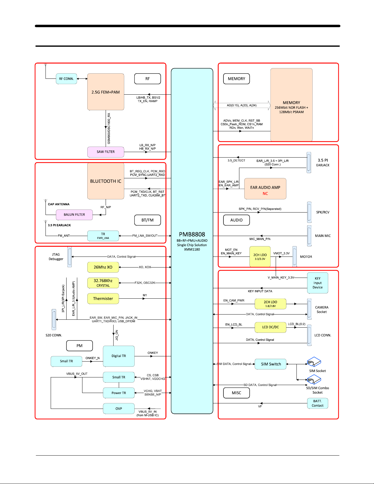
Block Diagram
8-1.
Repair
3
8-1
SAMSUNG Proprietary-Contents may change without notice
This Document can not be used without Samsung's authorization
Level3Repair
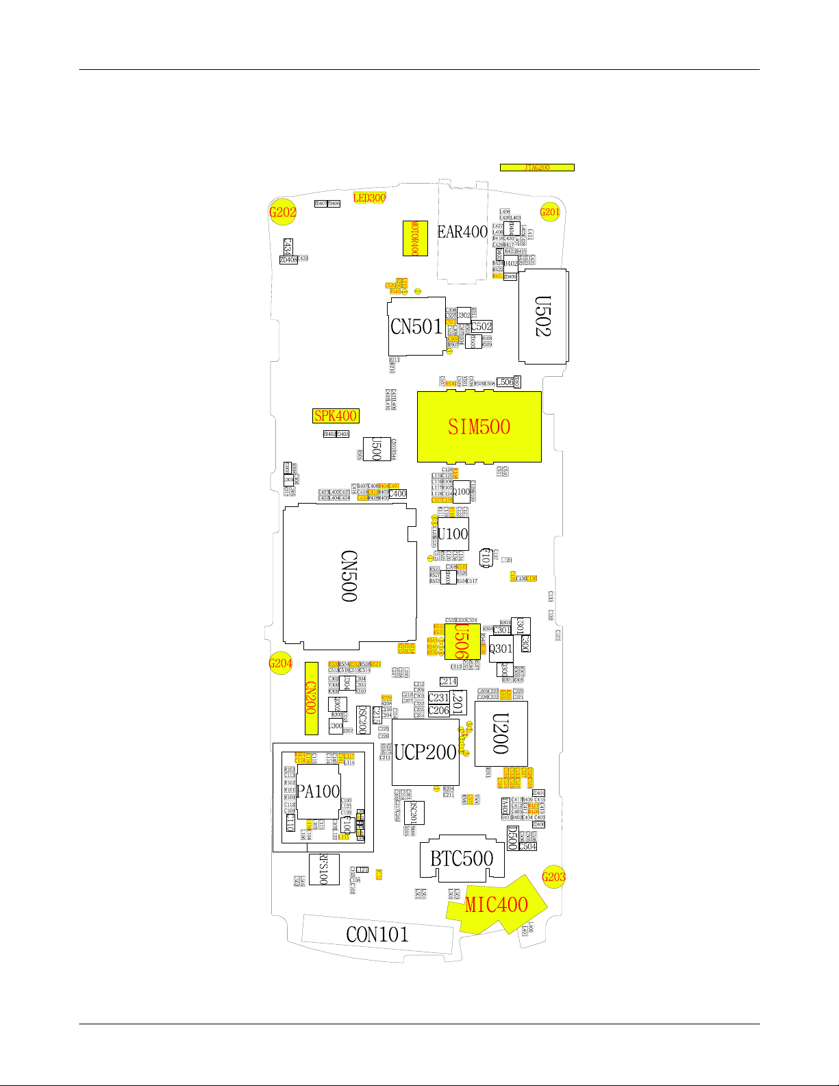
PCB Diagrams
8-2.
8-2-1.
Top
8-2
SAMSUNG Proprietary-Contents may change without notice
This Document can not be used without Samsung's authorization

Level3Repair
8-2-1.
Bottom
8-3
SAMSUNG Proprietary-Contents may change without notice
This Document can not be used without Samsung's authorization
Level3Repair
Flow Chart of Troubleshooting
8-3.
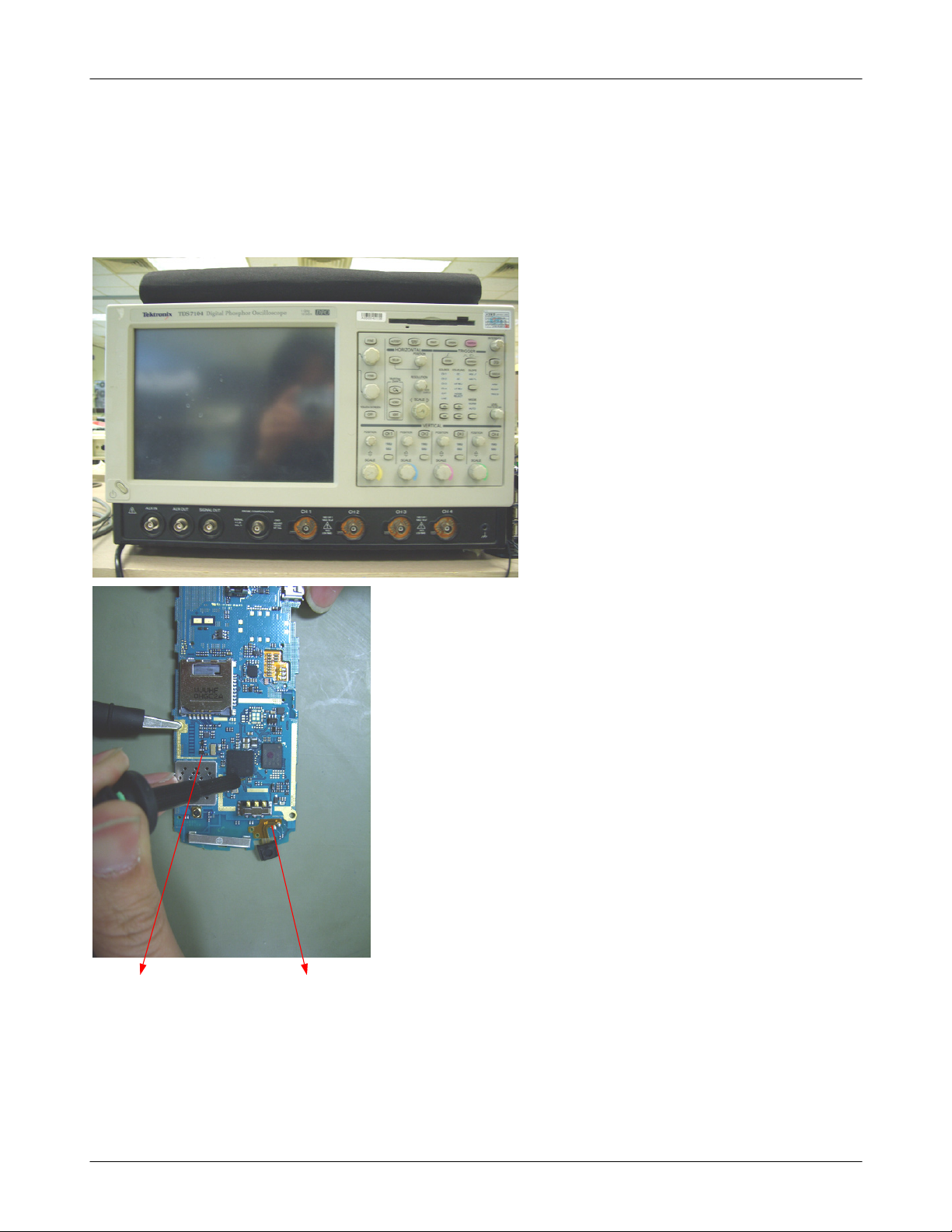
presetting methods for checking TP
(
GND&TP(ex. TP_VDDFS) using Oscilloscope
-
look over the coming out signal.
-
GND TP(TP_VDDFS)
Oscilloscope
8-4
SAMSUNG Proprietary-Contents may change without notice
This Document can not be used without Samsung's authorization

Multi-meter
Level3Repair
EX) to look up the TP, shunt Cap.
-
SAMSUNG Proprietary-Contents may change without notice
This Document can not be used without Samsung's authorization
Checking the TP(test point) using Multi-meter
if checking the GND, you can listen"beep".
-
if checking the Signal, you can't listen it.
8-5
Level3Repair
LOGIC
8-3.
8-1.
Power On
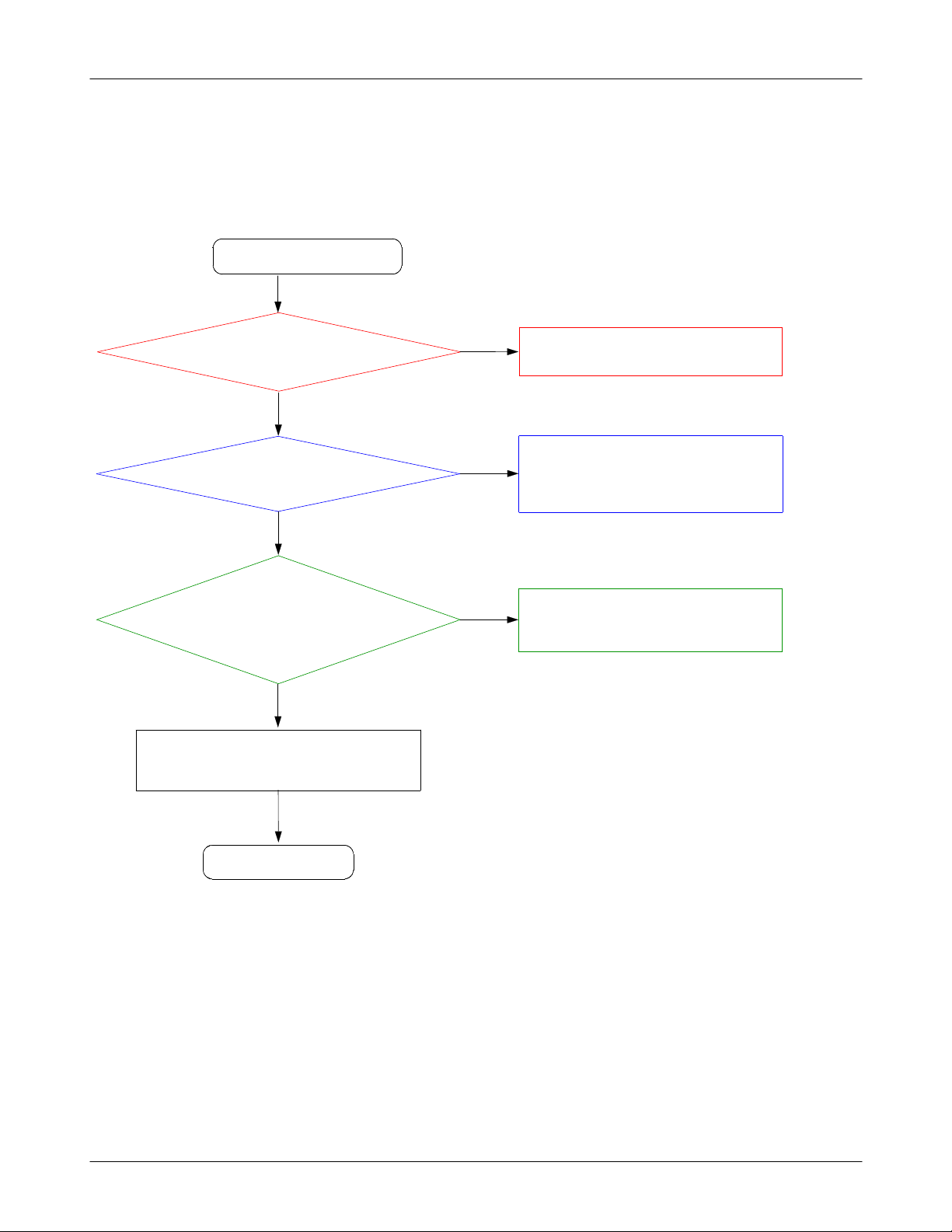
Check the Battery Voltage
VDD_1.8V
Check the Clock at
TP:OSC201
(
Initial Failure
is more than
=1.8
TP: C216)
(
Yes
UCP200 A11pin
CLK26M)
(
=26M
1,3
3.7V
V?
HZ
pin
Change the Battery
No
No
)
Check the Main Chip related to
SD1_FB=1.8V(TP:C231)
to lookover the Chip damage)
(
Check the Main Chip
to lookover the Chip damage)
(
Yes
Check the initial operation
Yes
END
8-6
SAMSUNG Proprietary-Contents may change without notice
This Document can not be used without Samsung's authorization

VBAT
BTC500
1
1
2
2
3
3
4
NC
5
0
NC
0
6
5
NC
V
7
NC
BATT.CON
Level3Repair
0
0
5
D
C506
R545
5
0
0
1
C537
NC
C504
C505
100
1005
C536
VF
UCP200
PMB8808
R14
HSL
T14
HSR
A11
XO
B11
XOX
R9
ONOFF
R7
SD1SW
T6
SD1_FB
R3
ADV_N
J1
RD_N
L13
RESET_N
H15
TRST_N
J6
WAIT_N
R4
WR_N
K16
TRIG_IN
B4
EAR_SPK_L
EAR_SPK_R
ONKEY
ADVn
RDn
TRSTn
WAITn
WEn
RST_BB_J
RST_BB
VDD_IO1_1.8V
OSC201
VDD_1.8V
C231
21
4
3
L201
R208
8-7
SAMSUNG Proprietary-Contents may change without notice
This Document can not be used without Samsung's authorization
Level3Repair
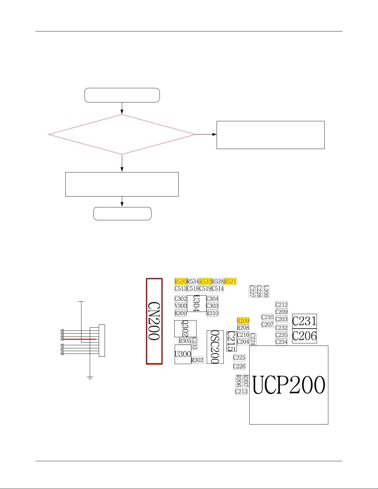
8-2.
Initial
Initial Failure
Yes
CN200(RST_BB_J
using the oscilloscope GND
SHORT PAD.
) > 1.7V?
Yes
Check the16bit data signal
memory CE
&
Yes
END
&
No
R
Resolder UCP
ST_BB_J)must be higher than
200
1.7
V.
RST_BB_J
TRSTn
TXD1_J
RXD1_J
VDD_IO1_1.8V
CN200
KARAT-JTAGPAD
1
1
2
TMS
TDI
TCK
TDO
2
3
3
4
4
5
5
6
6
7
7
8
8
9
9
10
10
8-8
SAMSUNG Proprietary-Contents may change without notice
This Document can not be used without Samsung's authorization
Level3Repair
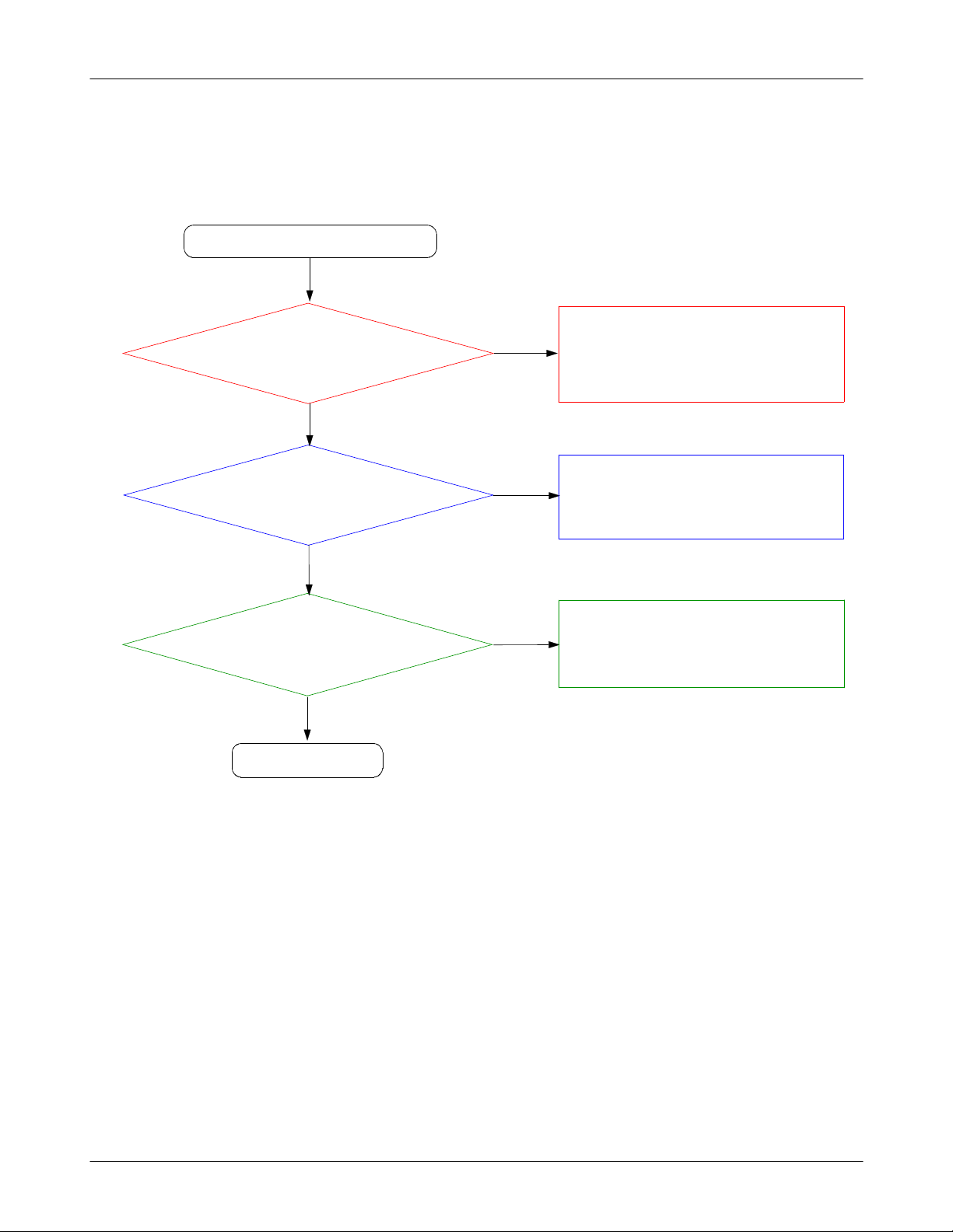
8-3.
Charging Part
Abnormal charging part
Check the Battery&TA
connection.
R306
> 4.9V?
Yes
Yes
Yes
No
No
Reinsert the Battery or TA.
Resolder R306
Check the Q301 pin
Yes
END
4 > 4.9V ?
No
Replace Q301 usingaHeatgun
8-9
SAMSUNG Proprietary-Contents may change without notice
This Document can not be used without Samsung's authorization
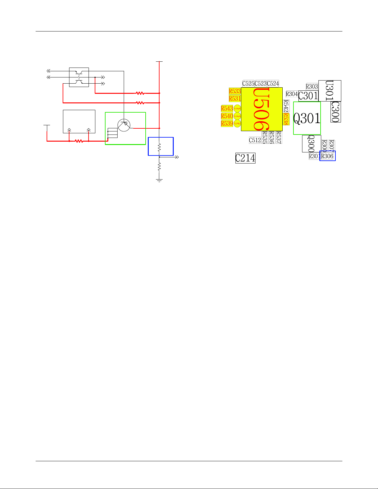
Level3Repair
CS
VBAT
Q300
1
2
34
N
_
E
S
N
E
S
R304
6
5
P
_
E
S
N
E
S
TNHSVBSC
VDDCHG
1
2
5
6
CHARGING CIRCUIT
VBUS_5V_OUT
R300
R301
3
4
Q301
R306
VCHG
R307
8-10
SAMSUNG Proprietary-Contents may change without notice
This Document can not be used without Samsung's authorization
Level3Repair
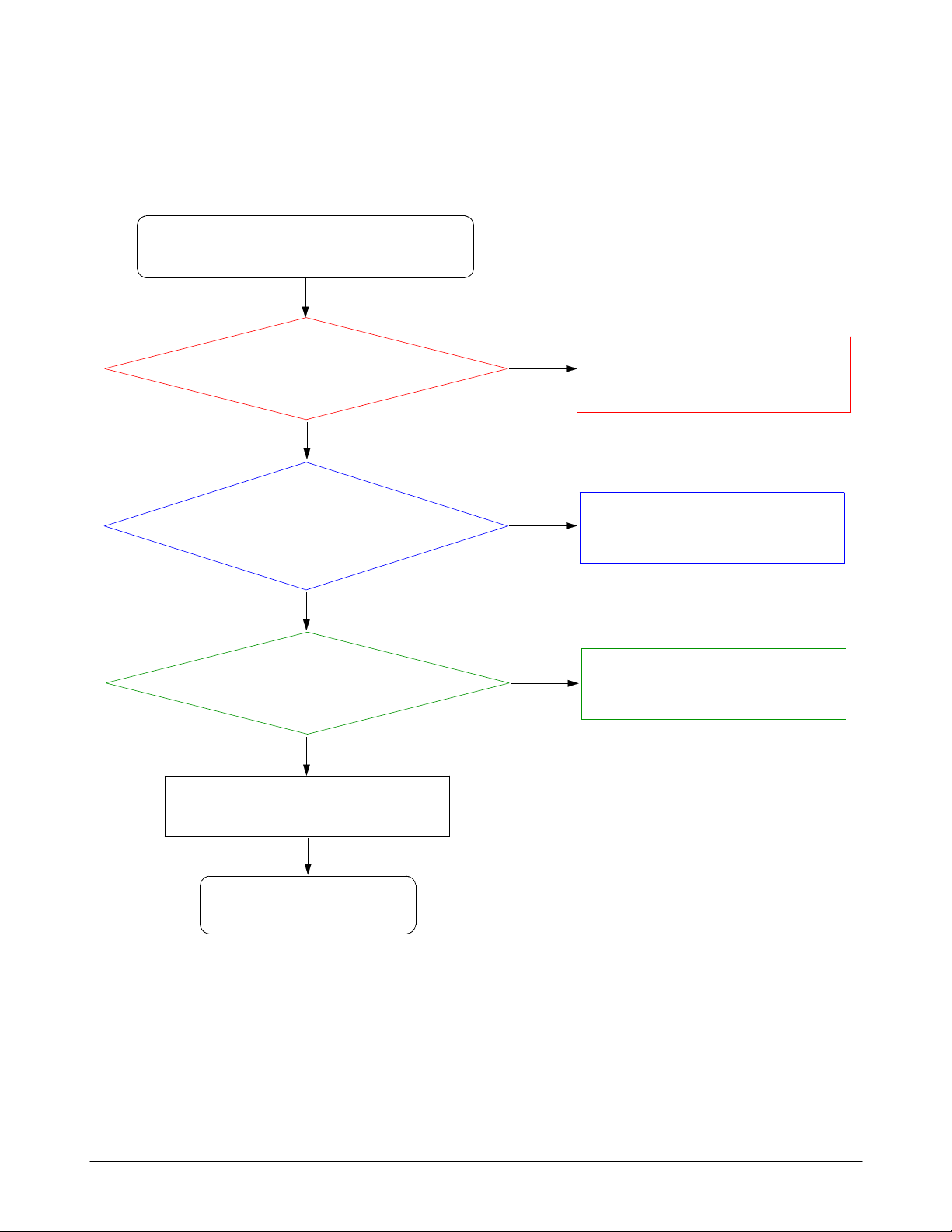
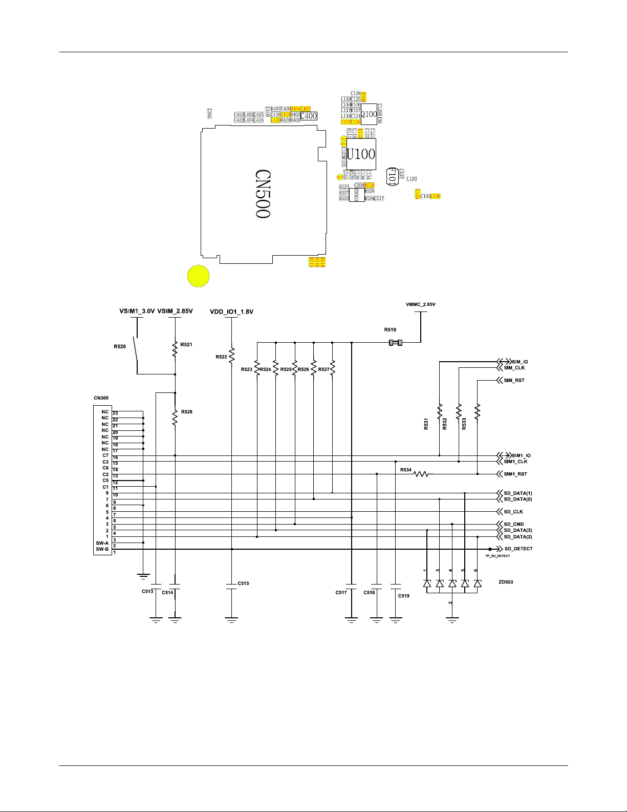
8-4-1.
Sim1Part
Phone can't access SIM Card
Check SIMCLK Signal on
pin3 of CN500 inafew second
Yes
CN500 pin
or R521="H"
After Power ON,
1
Yes
No
Resolder R521, R528, R531,
?
No
R532, R533, C514
Resolder or Replace CN500
Yes
After SIM card insert,
CN500 pin
Check the SIM Card
="
END
SIM_RST)
13(
H"?
Yes
Yes
No
Replace PBA
8-11
SAMSUNG Proprietary-Contents may change without notice
This Document can not be used without Samsung's authorization
Level3Repair
8-12
SAMSUNG Proprietary-Contents may change without notice
This Document can not be used without Samsung's authorization
 Loading...