

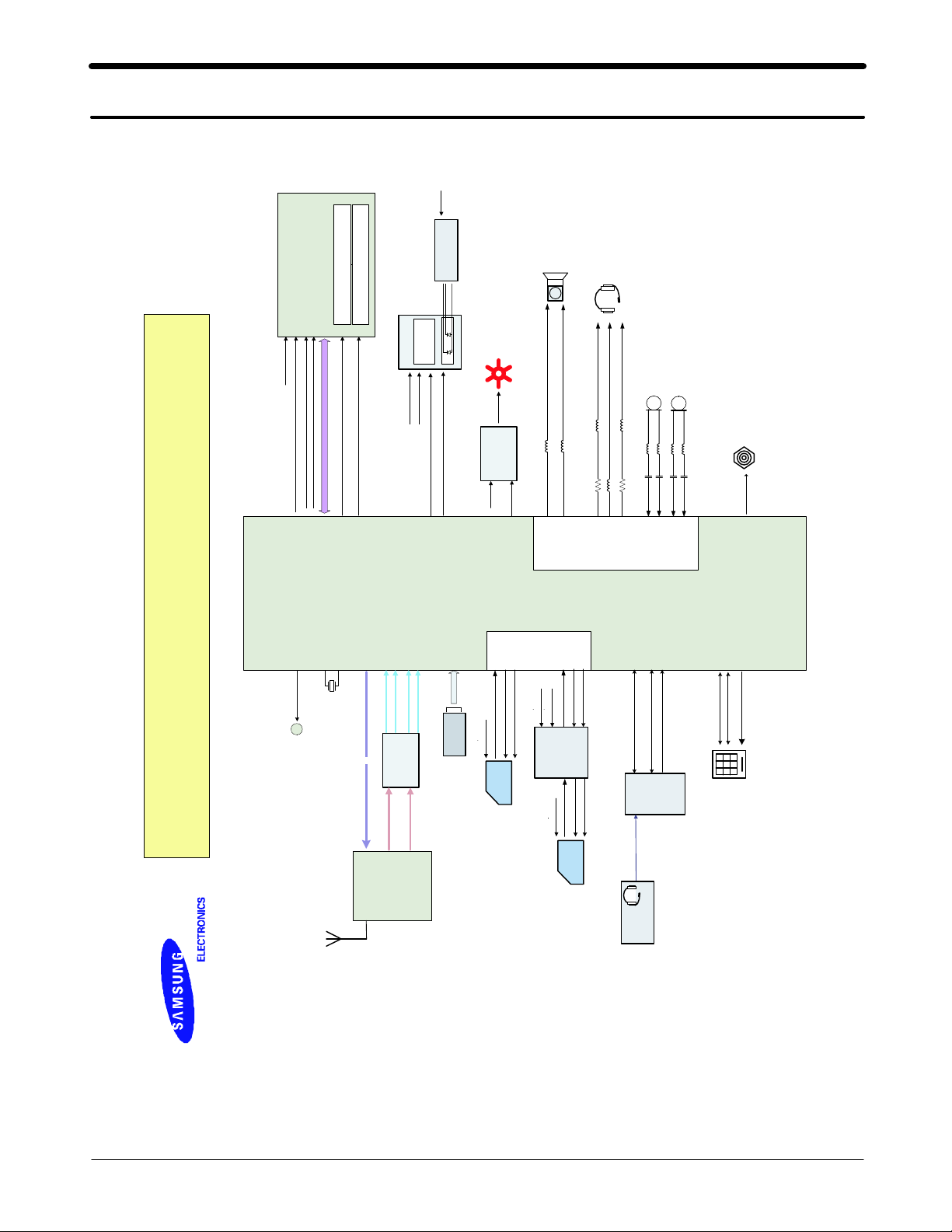
Samsung E1182 Block Diagram 7
Level
8.
Block Diagram
8-1.
m
a
r
g
a
i
D
k
c
o
l
B
2
8
1
1
E
T
G
3
Repair
p
U
k
c
a
B
T
A
B
V
)
H
Y
D
R
3
Y
O
0
M
E
M
E
N
O
H
P
V
8
.
1
_
M
M
A
E
R
M
S
V
C
n
T
N
E
S
/
W
R
/
H
S
n
S
Y
E
A
S
O
L
F
_
S
C
N
p
a
C
r
e
p
u
S
M
b
M
0
5
0
3
F
8
3
F
P
(
b
R
A
M
M
8
O
4
R
2
t
6
N
1
U
#
D
V
A
*
)
5
1
(
A
/
)
K
3
L
2
:
C
7
*
)
1
(
4
B
1
A
(
U
/
A
/
)
/
5
B
1
#
L
:
T
0
I
(
A
D
W
M
R
/
Y
D
R
F
*
)
3
1
(
A
P
N
_
_
X
z
H
k
8
6
7
.
2
3
X
R
R
X
X
C
C
D
D
r
e
t
l
i
F
X
T
W
A
S
X
R
X
C
D
)
4
7
M
1
7
A
F
P
R
(
)
X
.
S
v
2
r
2
D
6
5
D
E
M
L
A
F
(
/
2
1
K
K
_
_
D
D
E
E
L
L
A
D
)
G
8
C
2
V
L
1
Q
x
N
Q
8
I
2
T
A
1
(
F
M
T
A
V
V
_
8
8
.
D
.
1
2
E
_
L
O
/
I
M
n
P
E
e
G
M
O
V
/
V
T
n
e
S
R
W
/
S
)
0
Y
2
S
(
A
/
)
0
(
S
C
N
/
)
7
:
0
(
D
M
m
e
d
o
M
P
N
_
_
X
X
R
R
M
M
S
S
G
G
E
E
y
r
)
h
e
d
t
r
t
A
a
a
m
d
B
0
n
0
n
a
t
)
2
0
0
Y
P
2
4
9
R
F
S
(
X
R
M
S
G
E
0
o
I
S
1
-
(
i
L
H
C
R
O
T
)
C
D
I
1
r
3
D
3
L
H
9
C
0
1
R
P
O
R
T
(
N
T
E
_
A
H
B
V
C
R
O
T
)
2
5
8
4
X
N
P
(
A
T
T
K
S
L
A
R
C
D
_
_
_
M
M
M
I
I
I
V
S
S
S
0
.
3
_
1
M
I
S
V
t
e
1
k
M
c
I
o
S
S
R
E
V
I
E
C
E
R
&
K
P
P
N
_
_
S
K
K
P
P
S
S
M
I
S
A
T
T
K
S
L
A
R
C
D
_
V
_
_
2
5
2
2
8
M
.
M
M
I
I
I
2
T
S
S
S
_
A
B
B
A
B
B
B
B
N
B
V
A
V
r
&
)
e
t
h
Y
f
i
c
5
t
h
i
5
S
5
w
l
4
S
e
T
v
E
M
e
(
I
L
S
A
T
T
K
S
L
A
V
R
C
D
0
_
_
_
.
2
2
2
3
_
M
M
M
I
I
I
2
S
S
S
M
I
S
V
t
e
2
k
M
c
I
o
S
S
K
P
S
R
A
E
C
I
M
R
C
I
A
E
M
P
N
_
_
C
C
I
I
P
N
_
_
M
M
C
_
C
_
I
I
X
X
M
M
U
U
A
A
T
U
N
P
_
_
O
_
R
R
A
A
M
E
E
C
V
O
T
I
R
D
A
U
P
A
E
C
A
)
F
A
D
R
S
/
E
L
R
T
C
_
S
N
(
M
I
F
C
2
I
)
O
1
I
1
2
M
D
1
F
R
A
A
(
R
a
n
n
e
t
n
A
M
F
)
t
n
A
k
c
a
t
J
e
r
a
S
E
d
0
a
2
e
S
(
H
)
4
:
0
(
(
W
L
O
R
_
_
Y
M
E
K
F
D
A
P
Y
E
K
R
O
T
O
M
T
A
B
V
)
V
4
3
:
.
0
3
(
(
_
L
D
O
E
C
L
_
_
Y
Y
E
E
K
K
C
8-1
SAMSUNG Proprietary-Contents may change without notice
This Document can not be used without Samsung's authorization
Level3Repair
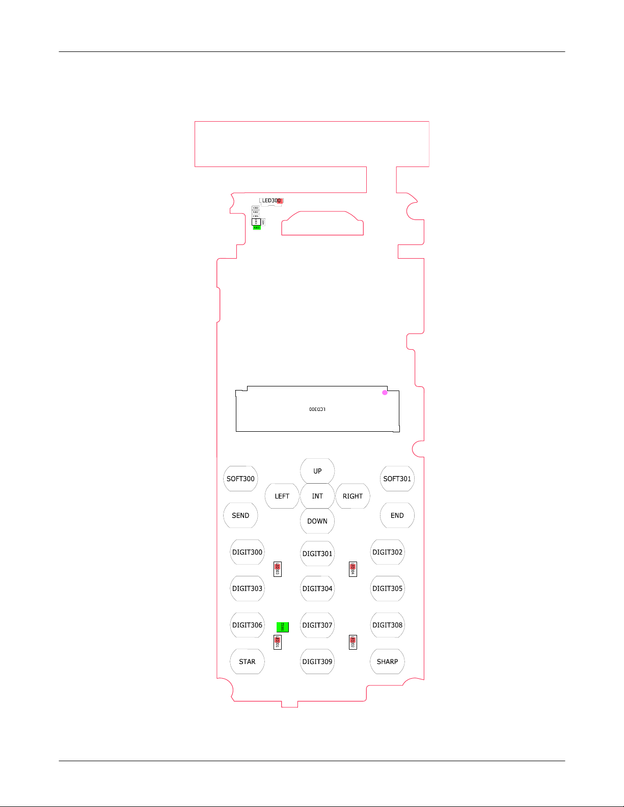
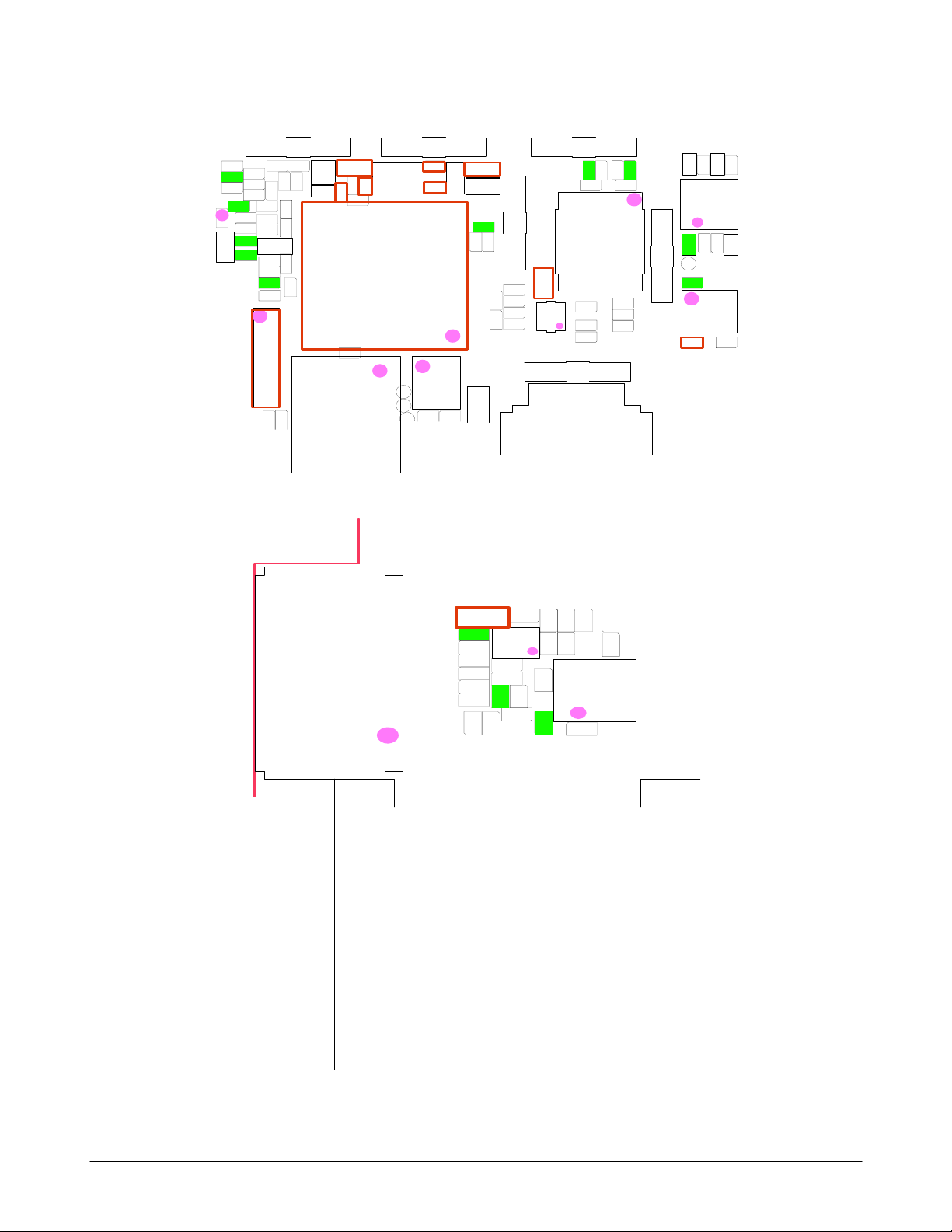
PCB Diagrams
8-2.
8-2-1.
Top
8-2
SAMSUNG Proprietary-Contents may change without notice
This Document can not be used without Samsung's authorization
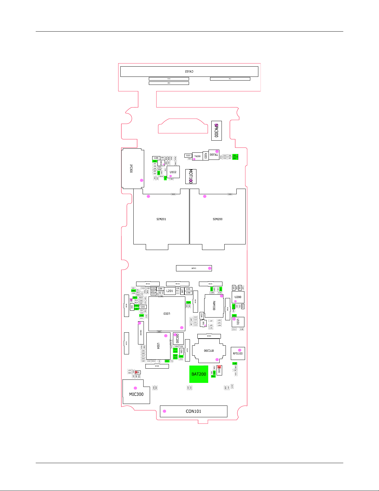
Level3Repair
8-2-1.
Bottom
8-3
SAMSUNG Proprietary-Contents may change without notice
This Document can not be used without Samsung's authorization
Level3Repair
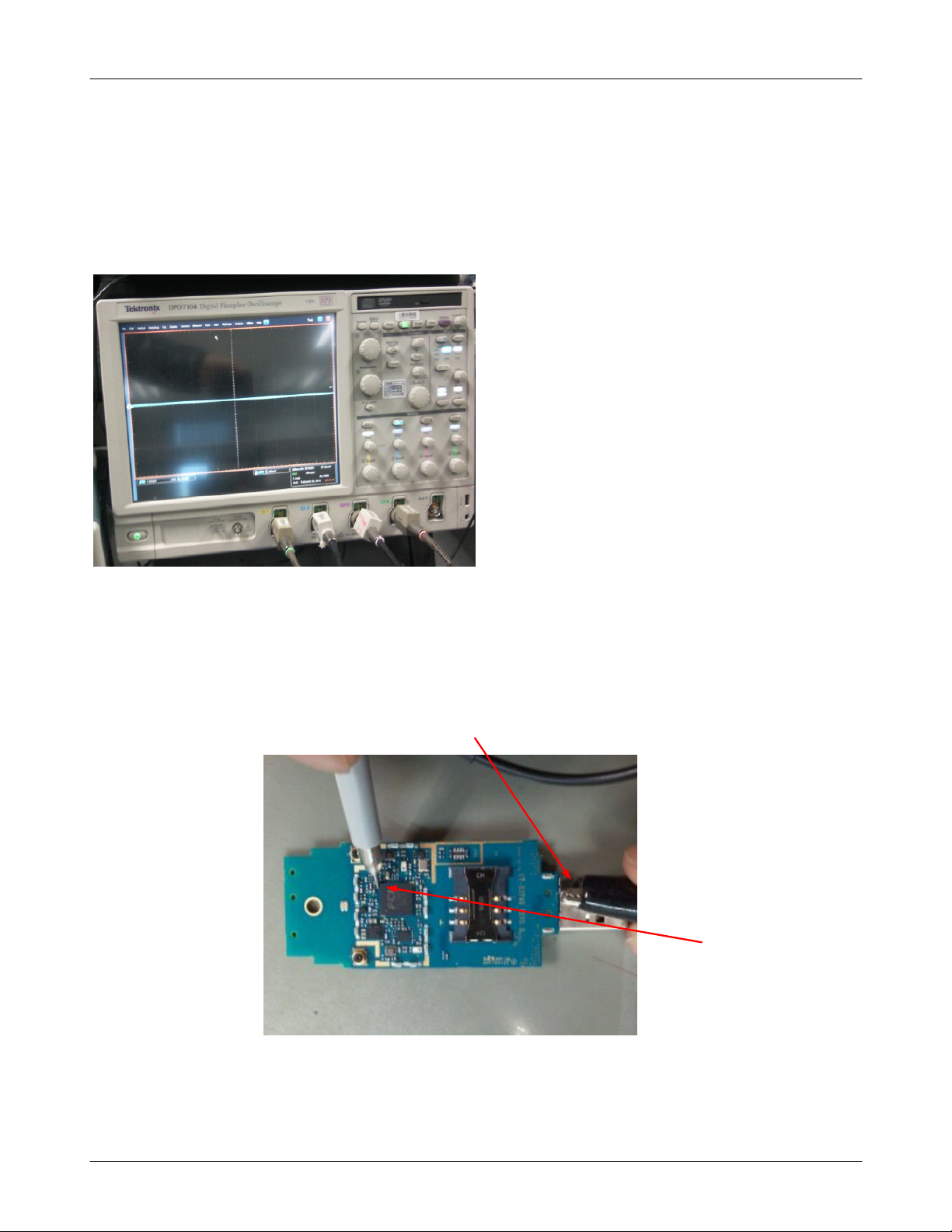
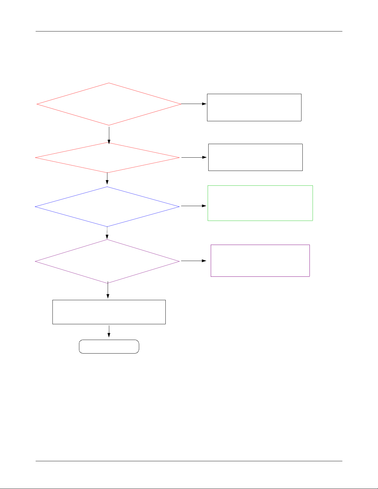
Flow Chart of Troubleshooting
8-3.
presetting methods for checking TP
※
GND&TP(exp. VBUS_5.0V=
-
look over the coming out signal.
-
C594~
C599) using Oscilloscope
GND
Oscilloscope
←
TP(Test Point)
8-4
SAMSUNG Proprietary-Contents may change without notice
This Document can not be used without Samsung's authorization
Level3Repair
8-3-1.
Power On
Check the Battery Voltage
is more than
TP:C104,C1
(
PMU_VIO
TP:C209, C316)
(
Check the Clock at
U303 L16pin(CLK32K)
TP:OSC201
(
C212,C308)
14,
Yes
=2.8
Yes
Yes
3.7V
V?
)
=32
KHZ
No
No
Change the Battery
Because of batt. power low)
(
Check the Main Chip related to
GPIO_2.8V(TP:C209, C316)
V
Check the Main Chip
OSC201/look over the waverform
(TP:
using the oscilloscope)
VCORE
+
TP:C206,C214, L201)
(
Check the initial operation
_1.25V
V?
=1.25
Power On"
"
END
Yes
Yes
No
Resolder C206, C214 and L201
to confirm coming out power V_core)
(
8-5
SAMSUNG Proprietary-Contents may change without notice
This Document can not be used without Samsung's authorization
Level3Repair
1
0
C
5
S
C311
C310
C309
C319
U
3
0
R313
6
R314
C
3
C325
2
1
C307
C102C103
C230
R207
C231
C206
C
C
L201
2
2
0
1
C
7
4
3
1
6
C208
0
3
C220
U
3
0
R
R311
R310
R208
R
1
1
0
0
C
1
0
2
2
7
C
2
R210
3
3
C320
R
3
1
5
C324
C232
C
3
0
C301
2
C303
R
2
C306
1
2
C211
O
S
C
2
0
1
R
R
2
2
1
S
0
C
8
C209
L
C201
2
0
R211
0
C200
C212
6
0
1
C
R204
S
R
R
1
1
0
0
3
2
U
3
C113
L
1
0
8
C112
L
C111
1
0
6
C110
O
S
C
2
0
TP203
0
T
P
2
0
1
2
0
R209
TH200
2
SC101
C
1
0
4
L107
0
0
1
F
L105
C151
SC100
C
C
C
C
1
1
1
1
5
0
0
4
0
0
9
1
C105
R110
P
A
M
1
0
0
L102
L101
L109
C
C
R
C
2
2
2
2
2
2
0
3
9
8
6
7
U200
C
C
C
R
2
2
2
2
3
3
3
1
6
4
5
3
S
C
1
0
5
2
0
2
P
T
R107
U
1
0
1
C114
R108
R
R
R
3
0
6
R
3
1
7
3
0
5
U102
C146
R
2
1
9
C
1
4
8
3
R304
R318
0
8
1
R
3
0
0
3
9
D
Z
C
1
4
1
R
3
0
7
C
1
4
7
C308
C326
I
F
C
3
0
0
L302
L306
L305
L304
L303
R301
R300
C
3
0
0
L
L
3
3
0
1
1
9
8-6
SAMSUNG Proprietary-Contents may change without notice
This Document can not be used without Samsung's authorization
Level3Repair
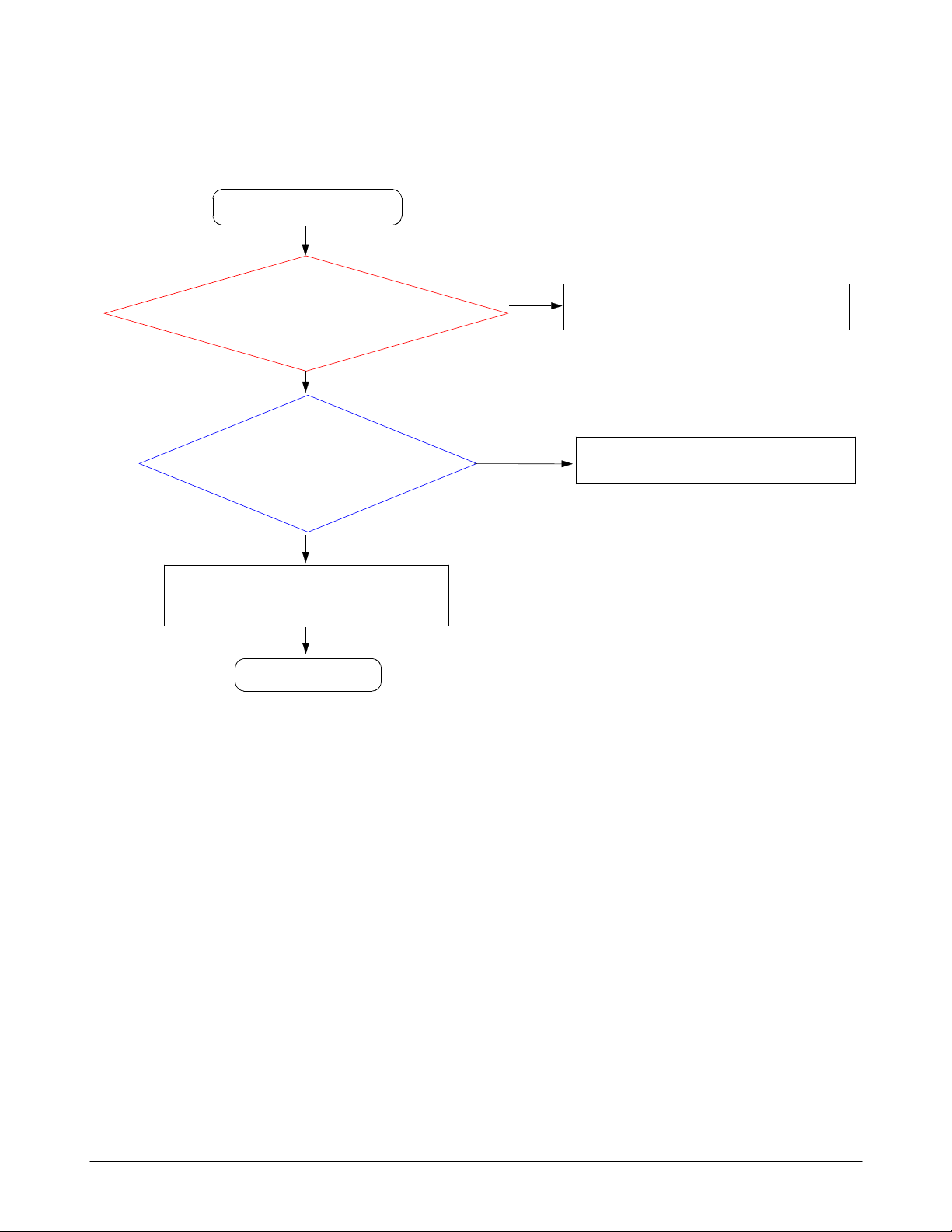
8-3-2.
Initial
Initial Failure
Yes
U300 pin T4(RSTON)
using the oscilloscope GND&TP
="H(>2.4V)"?
Yes
in M4 or D12=
U300 p
Check the16bit data signal
4V)"?
TP:LCD PIN5)
(
memory(TP:TP200)
&
"H(>2.
Yes
No
No
Replace U300, must be"H"
Change PBA
to check LCD PIN5)
(
END
Yes
8-7
SAMSUNG Proprietary-Contents may change without notice
This Document can not be used without Samsung's authorization
 Loading...