

Page 1
Level
8.
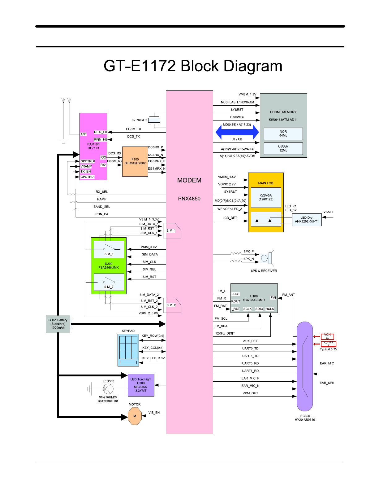
Block Diagram
8-1.
Repair
3
8-1
SAMSUNG Proprietary-Contents may change without notice
This Document can not be used without Samsung's authorization
Page 2
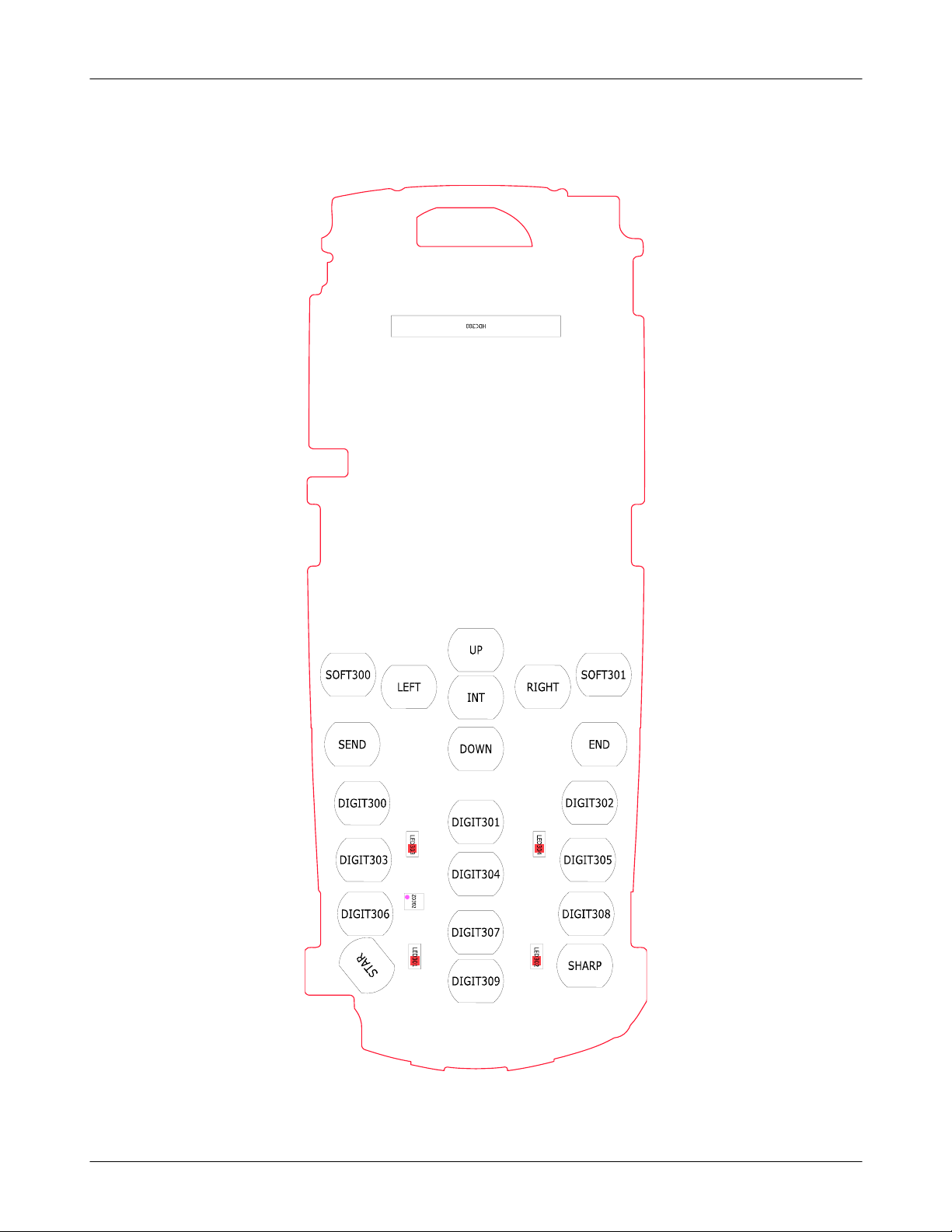
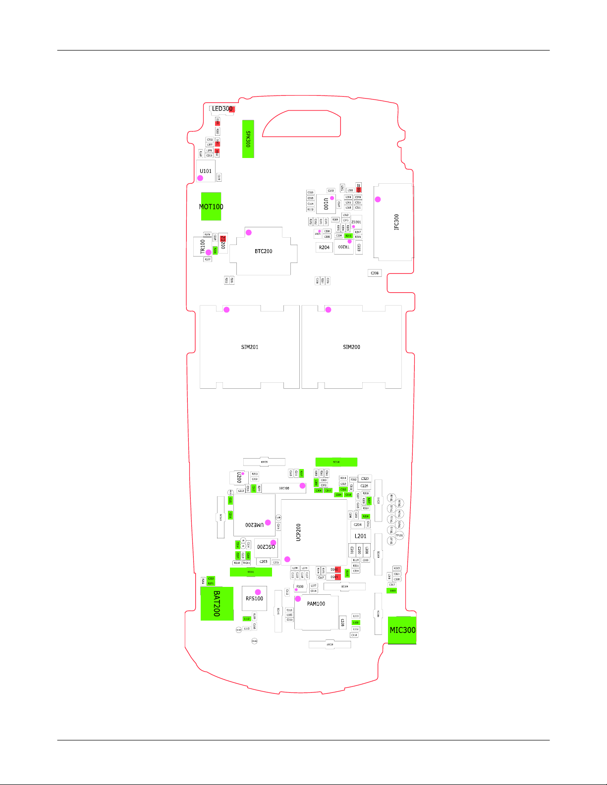
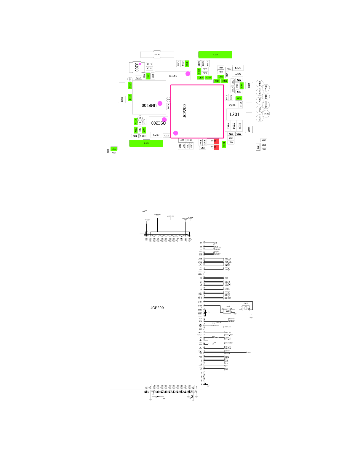
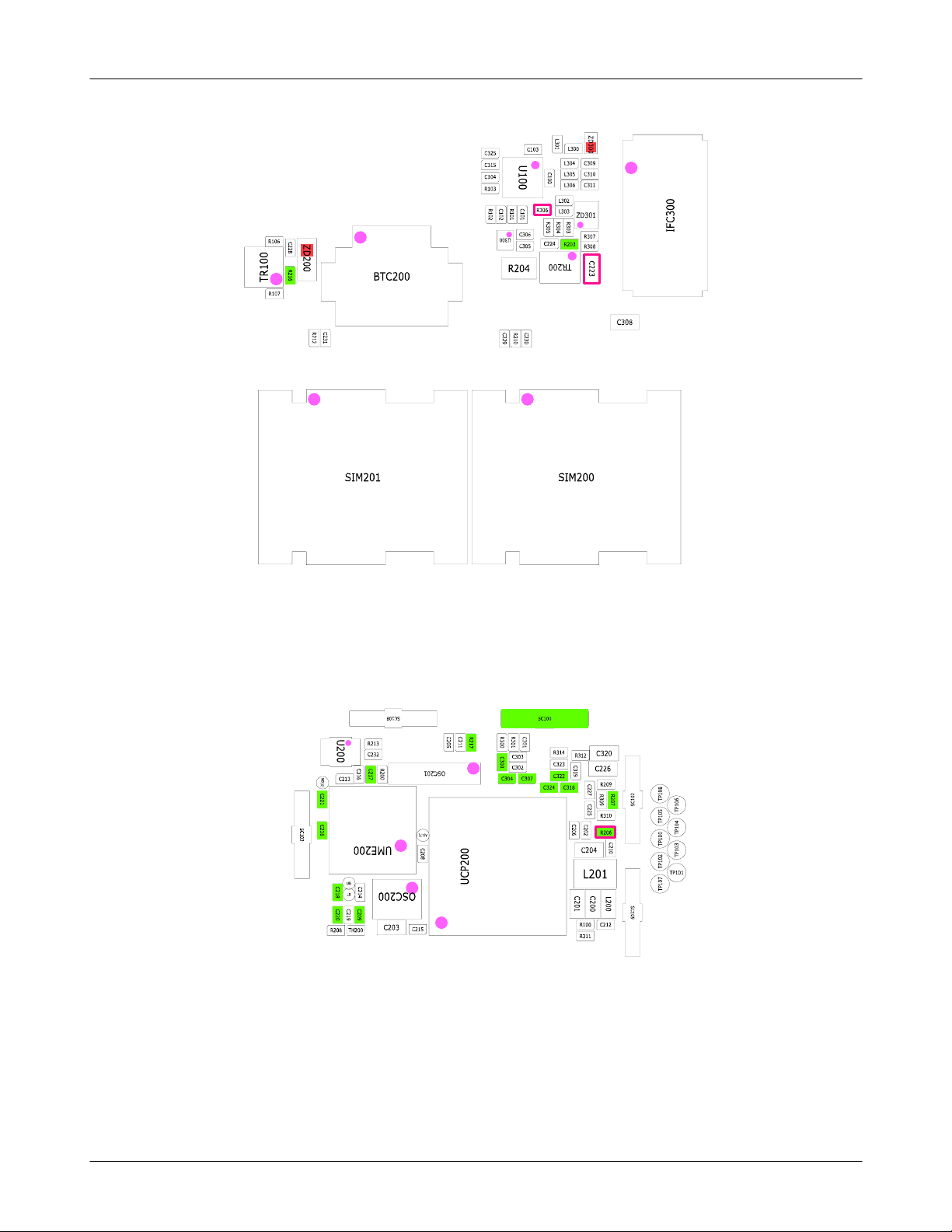
PCB Diagrams
8-2.
8-2-1.
Top
Level3Repair
8-2
SAMSUNG Proprietary-Contents may change without notice
This Document can not be used without Samsung's authorization
Page 3
Level3Repair
8-2-1.
Bottom
8-3
SAMSUNG Proprietary-Contents may change without notice
This Document can not be used without Samsung's authorization
Page 4
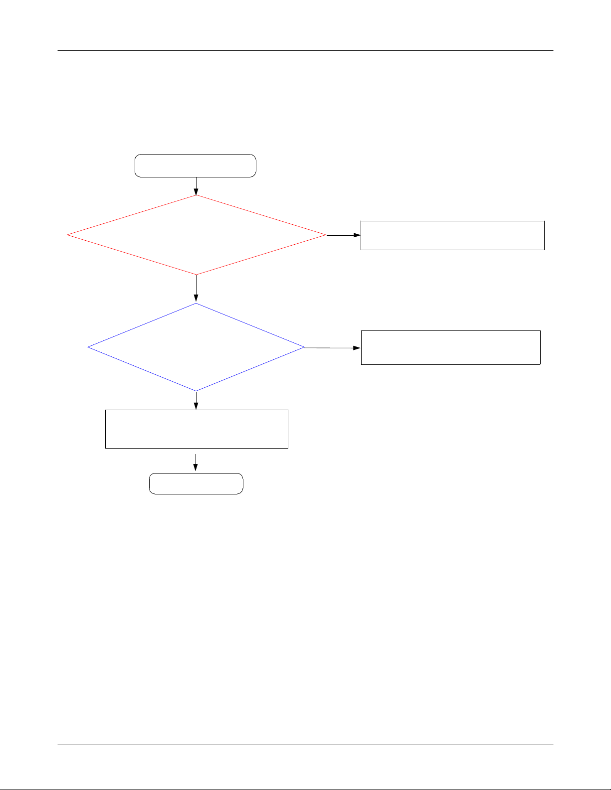
Flow Chart of Troubleshooting
8-3.
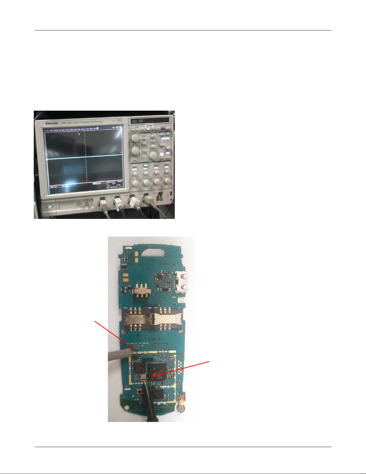
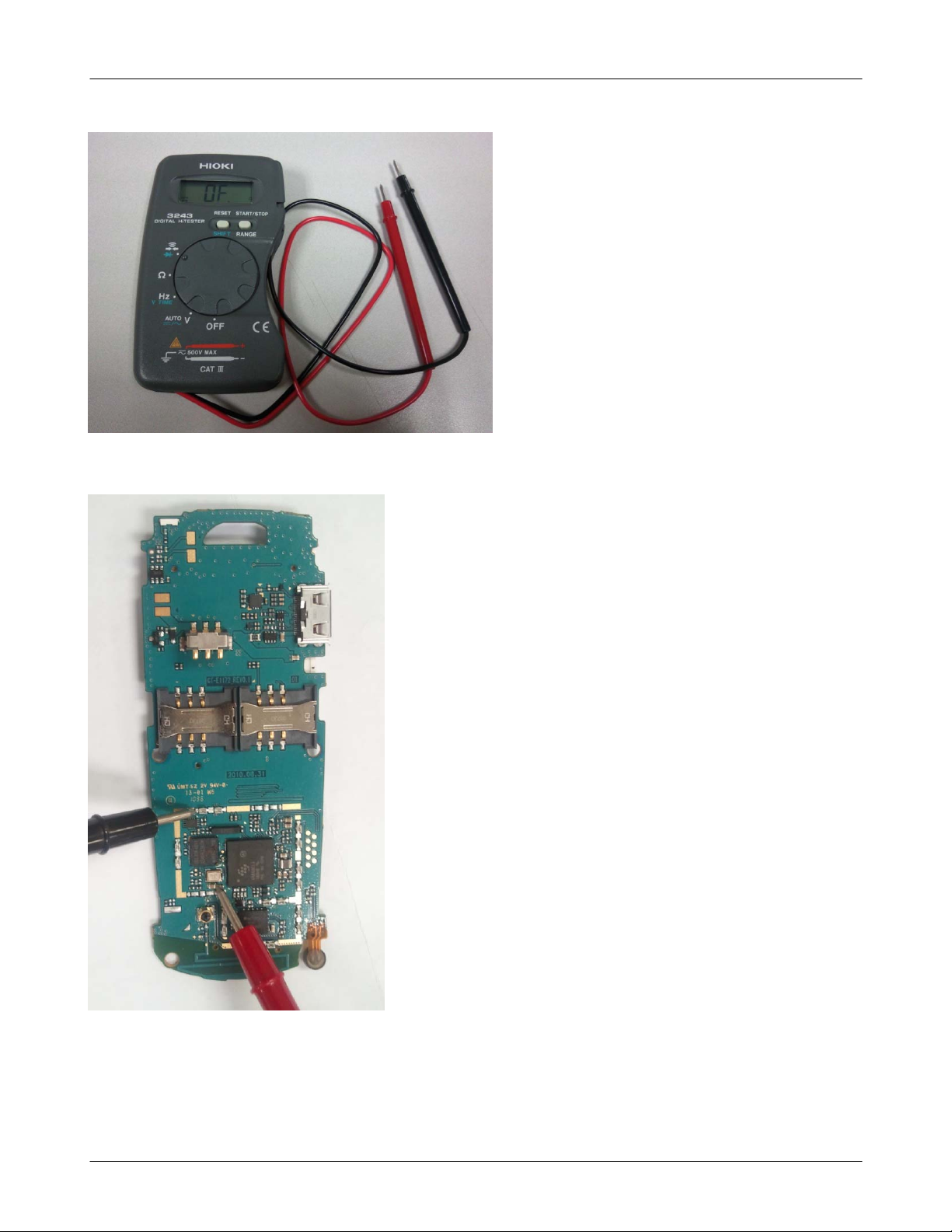
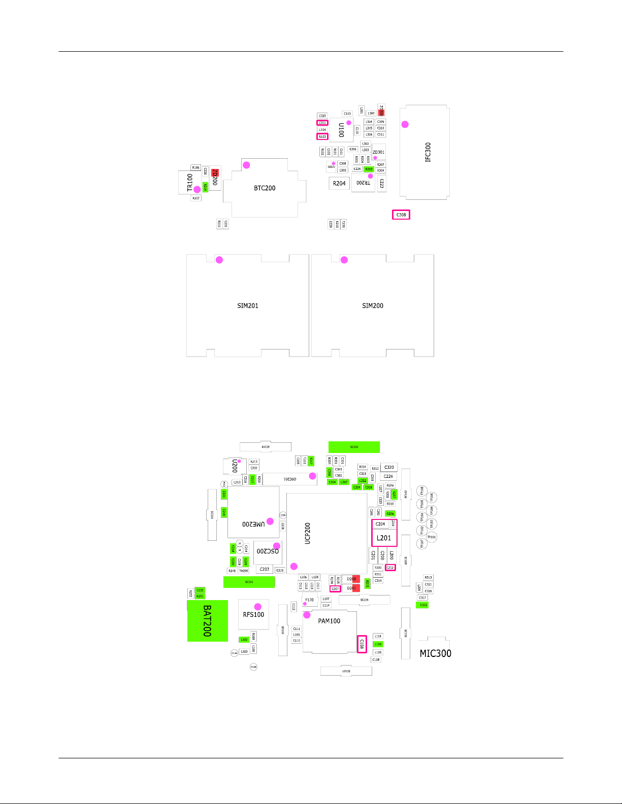
presetting methods for checking TP
GND&TP(exp. Vbatt=C108, C109, C212, C308)using Oscilloscope
look over the coming out signal.
-
Level3Repair
GND
Oscilloscope
TP(Test Point)
8-4
SAMSUNG Proprietary-Contents may change without notice
This Document can not be used without Samsung's authorization
Page 5
Level3Repair
Multi-meter
EX) to look up the TP, shunt Cap.
-
SAMSUNG Proprietary-Contents may change without notice
This Document can not be used without Samsung's authorization
Checking the TP(test point) using Multi-meter
if checking the GND, you can listen"beep"
if checking the Signal, you can't listen it.
8-5
Page 6
Level3Repair
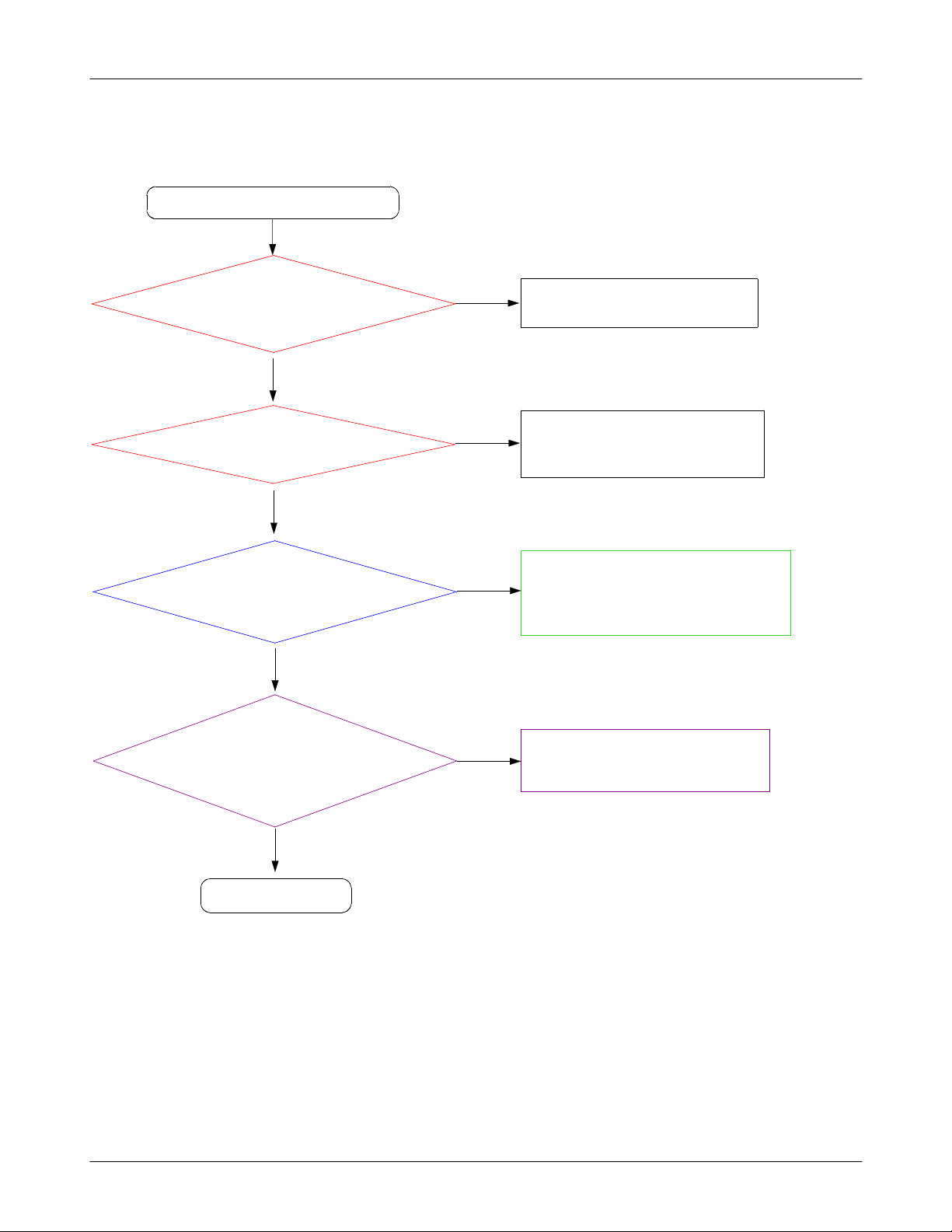
8-3-1.
Power On
Power On'does not work
'
Check the Battery Voltage
TP:C108, C109, C212, C308)
(
Yes
is more than
PMU_VIO
TP:C207, C315)
(
Check the Clock at
UCP200 L16pin
CLK32K)
(
TP:R103)
(
Yes
=2.8
Yes
=32
3.7V
V?
KHZ
No
No
No
Change the Battery
Because of batt. power low)
(
Check the Main Chip related to
GPIO_2.8V(TP:C207, C315)
V
to lookover the Chip damage)
(
Check the Main Chip
to lookover the Chip damage)
(
R103/look over the waverform
(TP:
using the oscilloscope)
VCORE
+
=1.25
TP:C204, C21
(
END
Yes
_1.25V
V?
,
0
Yes
L201)
No
Resolder C204, C214 and L201
to confirm coming out power V_core)
(
8-6
SAMSUNG Proprietary-Contents may change without notice
This Document can not be used without Samsung's authorization
Page 7
Level3Repair
8-7
SAMSUNG Proprietary-Contents may change without notice
This Document can not be used without Samsung's authorization
Page 8
Level3Repair
8-8
SAMSUNG Proprietary-Contents may change without notice
This Document can not be used without Samsung's authorization
Page 9
Level3Repair
8-3-2.
Initial
Initial Failure
Yes
UCP200 pin T4(RSTON)
="H(>2.4V)"?
TP106)
using the oscilloscope GND&TP
(TP:
Yes
CP200pin M4 or D12=
U
"H(>2.4V)"?
TP:TP100, LCD PIN5)
(
No
No
Replace UCP200, must be"H"
usingaHeatgun
Change PBA to check TP100&LCD PIN5
Yes
Check the16bit data signal
memory CE(TP:TP200)
&
Yes
END
8-9
SAMSUNG Proprietary-Contents may change without notice
This Document can not be used without Samsung's authorization
Page 10
Level3Repair
8-10
SAMSUNG Proprietary-Contents may change without notice
This Document can not be used without Samsung's authorization
Page 11
Level3Repair
8-3-3.
Charging Part
UCP200 pin V10(VCHG_P)
UCP200 pin V9(AUX_DET
Abnormal charging part
Yes
>4.9V
TP:C223)
(
Yes
or R303
"L=2.8V"?
Yes
No
be possible that it's not soldering well)
(
)
No
Resolder R206, C223
Resolder or Replace R303
Must be"L=2.8V"
Check the UCP200 pin R9
1.4V
Yes
END
No
Replace UCP200 usingaHeatgun
8-11
SAMSUNG Proprietary-Contents may change without notice
This Document can not be used without Samsung's authorization
Page 12
Level3Repair
8-12
SAMSUNG Proprietary-Contents may change without notice
This Document can not be used without Samsung's authorization
Page 13

Level3Repair
8-3-4.
Sim Part
Phone can't access SIM Card
Yes
SIM
or R210
After Power ON,
Check SIM_CLK_1 Signal on
pin3 of SIM
method:wiring pin3and
(
checking its waveform using an
pin
200
"H=3.0V" ?
Yes
200ina
oscilloscope)
1
few second
No
No
Resolder R210, C230
insert SIM card&access it,
then must be sim pin1 or R210"H=3.0V"
Resolder or Replace SIM200 connector.
Because of not soldering well)
(
Yes
After SIM card insert,
SIM
method:wiring pin2and check
(
pin2(SIM_RST_1)
200
"H=3.0V"?
its waveform using an
oscilloscope) oscilloscope)
Yes
=
No
Confirm an another PBA(U200)
8-13
SAMSUNG Proprietary-Contents may change without notice
This Document can not be used without Samsung's authorization
Page 14

Level3Repair
SIM
or R212
After Power ON,
Check SIM_CLK_2 Signal on
pin3 of SIM
method:wiring pin3and
(
checking its waveform using an
method:wiring pin2and check
(
oscilloscope)
After SIM card insert,
SIM
201
its waveform using an
oscilloscope) oscilloscope)
pin
20
201ina
pin2(SIM_RST_2)
"H=3.0V"?
1
1
"H=3.0V" ?
Yes
few second
Yes
No
then must be sim pin1 or R212"H=3.0V"
No
=
No
Resolder or Replace SIM201 connector.
Resolder R212, C231
insert SIM card&access it,
Because of not soldering well)
(
Confirm an another PBA(U200)
Yes
Check the SIM Card
look over if it get damaged.)
(
Yes
END
8-14
SAMSUNG Proprietary-Contents may change without notice
This Document can not be used without Samsung's authorization
Page 15

Level3Repair
8-15
SAMSUNG Proprietary-Contents may change without notice
This Document can not be used without Samsung's authorization
Page 16

Level3Repair
8-3-5.
Microphone Part
Microphone does not work
UCP200 pin U18="H=2.85V"
at Mic Active
TP:C226)
(
Check the MIC Connection
look over schematics about
(
schemetics.)
Yes
Yes
Yes
?
No
No
Replace UCP200 usingaHeatgun
Because of not soldering well
(
Resolder C317, C326, L309, R313, C321, R312,
R314, C319, C323
not work if those is not connected.)
(
)
Check the MIC sample.
it be possible the problem
(
things)
Yes
END
No
Replace an another MIC
because of being possible the problem)
(
8-16
SAMSUNG Proprietary-Contents may change without notice
This Document can not be used without Samsung's authorization
Page 17

Level3Repair
8-17
SAMSUNG Proprietary-Contents may change without notice
This Document can not be used without Samsung's authorization
Page 18

Level3Repair
8-3-6.
Speaker Part
(
checking an waveform using
Does not work Voice call
Speaker does not work
Yes
UCP200 pin W18, W19
>3.7V
Wiring the SPK N/P and
oscilloscope)
Yes
Yes
No
(
No
?
Resolder C227 AND R209
be possible because of soldering not well)
Replace UCP200 usingaHeatgun
be possible of being UCPabad sample)
(
Does not work Ringtone?
Menu->settings->profiles
(
options->Edit->
->
select the Call ringtone)
Yes
Is Speaker working?
Listening through the
(
speaker)
Yes
END
No
No
Resolder or Replace UCP200, SPK300
be possible of soldering not well or being
(
UCPabad sample)
Change Speaker ASS'Y
be possible of SPK Problems
(
or not inserting it right.)
8-18
SAMSUNG Proprietary-Contents may change without notice
This Document can not be used without Samsung's authorization
Page 19

Level3Repair
P_KPS
N_KPS
213C
703L
803L
313C
103D
003KPS
203D
8-19
SAMSUNG Proprietary-Contents may change without notice
This Document can not be used without Samsung's authorization
Page 20

Level3Repair
8-3-7.
Key Data Input
Check Initial Operation
When you pushed all of the
Key, does the key have
Yes
tension?
Yes
No
(#1 :
whether be sunken
look over the Dome location
#2 :
whether be out of line)
Change Domesheet
look over the Dome situation
All of the key doesn't work
except POWER ON KEY
Yes
END
No
?
because of be possible for PBA to get damaged)
Replace the PBA
over the insturctions again
(
and change the board
8-20
SAMSUNG Proprietary-Contents may change without notice
This Document can not be used without Samsung's authorization
Page 21

Level3Repair
V3.3_DEL_YEK
113R
0584XNP ybraeN
413C
103DEL
303DEL
203DEL
403DEL
DEL YEK
)0(OIYEK
)1(OIYEK
)2(NIYEK
)1(NIYEK
)0(NIYEK
UOYEK
)0(T
)1(TUOYEK
)2(TUOYEK
)3(TUOYEK
)2(OIYEK
003TIGID
12
303TIGID
12
603TIGID
12
RATS
12
DNES
103TIGID
12
403TIGID
12
703TIGID
1
2
903TIGID
12
203TIGID
12
503TIGID
12
803TIGID
12
PRAHS
12
003TFOS
12
103TFOS
12
TFEL
1212
NWOD
12
TNI
2
1
PU
12
THGIR
12
1
203DZ
2
PAM YEK
6
5
4
3
8-21
SAMSUNG Proprietary-Contents may change without notice
This Document can not be used without Samsung's authorization
Page 22

Level3Repair
8-3-8.
Back Light(for Color Main LCD)
Backlight does not work
Yes
Is LCD Contrast set on high
level in the Menu?
menu->settings->display->light
(
Wiring pin
(
LCD contrast)
->
Is U101 pin
Yes
H>2.7V"
1="
LCD_BL_EN)
#1/
?
No
No
Set LCD Contrast on high level
menu->settings->display->light
(
LCD contrast/select5Level(level
->
Resolder U101
#1 :
with an soldering iron)
(
Repalce LCD Module
#2 :
to check if it has the problem)
(
:1~5)
END
Yes
8-22
SAMSUNG Proprietary-Contents may change without notice
This Document can not be used without Samsung's authorization
Page 23

Level3Repair
3
0
C
0
D
H
TABV
101U
NE_LB_DCL
2
DNG
A_DEL
701R
901C
801R
1K_DEL
2K_DEL
8-23
SAMSUNG Proprietary-Contents may change without notice
This Document can not be used without Samsung's authorization
Page 24

Level3Repair
8-3-9.
Key Back Light
Main Key LED does not work
UCP200 pin T8, V8
Wiring POWER ONKEY_1,
(
look over using an
Key LED does not work?
look over the LED light)
(
Yes
H=3.0V
"
"?
GND
&
Oscillocope)
Yes
=
2
No
No
Replace UCP200 usingaHeatgun
must be coming out the signal"H")
(
Replace the LED
be possible that the sample has the problem)
(
#1 :
#2 :
Change PBA
END
Yes
8-24
SAMSUNG Proprietary-Contents may change without notice
This Document can not be used without Samsung's authorization
Page 25

Level3Repair
8-25
SAMSUNG Proprietary-Contents may change without notice
This Document can not be used without Samsung's authorization
Page 26

Level3Repair
presetting
Tx setting)
(
After setting
8960
8960 (
EGSM/DCS
Rx setting)
(
Active Cell
1.
select GSM or GPRS
:
Connetion Type
2.
select Auto(GSM), BLER(GPRS)
:
BCH Parameter
3.
select measuring band(DCS or EGSM)
:
Cell power
4.
dBm
:-60
)
After setting, prepare the call setup Display
1.
Using an Originate Call, makeacall.
2.
Confirm the display"connected"
3.
start the measuring
4.
8-26
SAMSUNG Proprietary-Contents may change without notice
This Document can not be used without Samsung's authorization
Page 27

Level3Repair
8960 &
spectrum analyzer
down&up at picture)
(
spectrum analyzer:testing method=the way using an Osciliscope
-
-8960:
connect using RF Cable between
8960 &
RF Connector in board.
RF Connector
8-27
SAMSUNG Proprietary-Contents may change without notice
This Document can not be used without Samsung's authorization
Page 28

Level3Repair
8-3-10.
GSM
Cell Power
PAM100
(
spectrum analyzer)
PAM100 Pin17
(
pin
TP:C116,C117 using
(
spectrum analyzer)
Receiver
900
RX ON
:-60
Yes
Pin
15
dBm
-65
TP:L111 using
Yes
dBm
-68
TP:L107 using
Yes
F10
0
7,6-70
dBm
dBm
No
No
No
Check PAM100 pin
Resolder F100
(L=0.4
V)
8
No
Yes
Check ANT Switch
control circuit
Resolder PAM100
Yes
Check&Resolder
C200, C201, C203, C204, L200,
And PMU Part and UCP20
Yes
END
0
8-28
SAMSUNG Proprietary-Contents may change without notice
This Document can not be used without Samsung's authorization
Page 29

Level3Repair
8-3-11.
DCS Receiver
RX ON
Cell Power
PAM100
(
spectrum analyzer)
PAM100 Pin18
TP:C114 using
(
specturm analyzer)
pin
TP:C113,C115 using
(
spectrum analyzer)
:-60
Yes
Pin
15
dBm
-65
TP:L111 using
Yes
dBm
-68
Yes
F10
0
8,9-70
dBm
dBm
No
No
No
Check PAM100
pin
pin10(H=2.4V)
Resolder F100
8(L=0.4
V)
No
Yes
Check ANT Switch
control circuit
Resolder PAM100
Yes
Check&Resolder
C200, C201, C203, C204, L200,
And PMU Part and UCP20
Yes
END
0
8-29
SAMSUNG Proprietary-Contents may change without notice
This Document can not be used without Samsung's authorization
Page 30

Level3Repair
001SFR
A21C3GG
4
011L
001L
111L
101L
601C
201L
811C
301L
001TNA
101TNA
XRMSGE
XRSCD
TABV
801C
L
E
A
S
L
_
P
E
_
D
S
N
_
N
X
O
A
R
P
B
PMAR
4
3
1
0
2
1
2
2
9
2
1
2
8
1
7
1
0
D
D
N
G
41
DNG
51
TNA
02
DNG
61
CN
D
D
N
T
P
L
L
T
E
N
N
N
M
R
R
_
A
G
G
G
A
T
T
X
B
R
T
C
C
V
V
P
P
G
G
0
0
1
M
A
P
D
D
D
D
D
0
1
N
N
N
N
N
C
X
X
C
N
R
G
G
G
G
G
R
N
3
5
1
6
2
8
9
7
3
1
1
1
1
1
501L
4
BL_NIFR
2
BH_NIFR
111C
011C
XT_MSGE
XT_SCD
211C
411C
XRSCD
1
701L
XRMSGE
4
001F
9
1NI
2NI
1TUO
8
1TUO
7
2TUO
6
2TUO
G
G
G
G
0
2
3
5
1
311C
601L
511C
611C
801L
711C
P_XRSCD
N_XRSCD
P_XRMSGE
N_XRMSGE
8-30
SAMSUNG Proprietary-Contents may change without notice
This Document can not be used without Samsung's authorization
Page 31

Level3Repair
8-31
SAMSUNG Proprietary-Contents may change without notice
This Document can not be used without Samsung's authorization
Page 32

Level3Repair
8-3-12.
GSM
TX ON(5Level)
PAM100
TP:L111 using
(
spectrum analyzer)
PAM100 pin4
TP:C111 using
(
spectrum analyzer)
900
30
dBm
Yes
Pin
dBm
No
Transmitter
15
-4
yes
Yes
CheckPAM
pin
Pin10(H=2.4V)
8(H=2.4
100
V)
No
Check ANT Switch
Yes
Change or Resolder
control circuit
PAM100
No
PAM100 pin2
dBm
-4
TP:C112 using
(
spectrum analyzer
No
Check&Resolder
C200, C201, C203, C204, L200,
And PMU Part and UCP20
Yes
END
0
Yes
Yes
Check PAM100
VBATT(pin11=3.7V)
TP:C108) OK?
(
Resolder or Change
L105, C110, C111
8-32
No
Yes
Change the UCP200
ifadamaged chip.
Check VBAT
using the osciliscope
TP:C108)
(
or PAM control signal
SAMSUNG Proprietary-Contents may change without notice
This Document can not be used without Samsung's authorization
Page 33

Level3Repair
8-3-13.
DCS Transmitter
TX ON(5Level)
Yes
PAM100
spectrum analyzer)
PAM100 pin
(
spectrum analyzer)
Pin
15
dBm
30
TP:L111 using
(
No
2-4
dBm
TP:C112 using
yes
Yes
CheckPAM
pin
Pin5(H=2.4V)
4(H=2.4
100
V)
No
Check ANT Switch
Yes
Change or Resolder
control circuit
PAM100
No
PAM100 pin
TP:C112 using
(
spectrum analyzer
Check&Resolder
C200, C201, C203, C204, L200,
And PMU Part and UCP20
dBm
-4
END
1
No
0
Yes
Yes
Yes
Check PAM100
VBATT(pin11=3.7V)
TP:C108) OK?
(
Resolder or Change
C112
8-33
No
Yes
Change the UCP200
ifadamaged chip.
Check VBAT
using the osciliscope
TP:C108)
(
or PAM control signal
SAMSUNG Proprietary-Contents may change without notice
This Document can not be used without Samsung's authorization
Page 34

Level3Repair
RFS100
A
1C3GG4
2
L110
L100
L111
DCSRX
EGSMRX
R109
C106
C118
L102 L103
C114
ANT100
ANT101
EGSMRX
DCSRX
F100
1
IN1
L107
4
IN2
G
G
2
3
VBAT
C108
9
OUT1
8
OUT1
7
OUT2
6
OUT2
G
G
5
0
1
L
E
A
S
L
_
P
E
_
D
S
N
_
N
X
A
O
B
P
R
RAMP
1
0
2
2
D
N
G
14
GND
15
ANT
20
GND
16
NC
3
1
4
1
1
7
8
9
2
2
2
1
0
D
D
D
T
P
N
L
L
T
E
N
N
N
M
R
R
_
A
G
G
G
A
T
T
X
B
R
T
C
C
V
V
P
P
G
G
RFIN_LB
0
0
1
M
A
P
RFIN_HB
D
D
D
D
D
1
0
N
N
N
N
N
C
C
X
X
N
G
G
G
R
G
G
N
R
6
5
3
1
2
3
7
9
8
1
1
1
1
1
C113
L105
4
2
C111
C110
EGSM_TX
DCS_TX
C112
DCSRX_P
L106
C115
C116
DCSRX_N
EGSMRX_P
L108
C117
EGSMRX_N
8-34
SAMSUNG Proprietary-Contents may change without notice
This Document can not be used without Samsung's authorization
Page 35

Level3Repair
8-35
SAMSUNG Proprietary-Contents may change without notice
This Document can not be used without Samsung's authorization
Page 36

Level3Repair
8-3-14.
Torch Light
Torch Light LED does not work
Yes
Check LED300.C306,R302
Is it broken or damaged?
No
Check U300
pin
1
Yes
Check U300
pin
1
Yes
Resolder or Replace LED300.C306,R302
No
Change PBA
No
Change U300
END
Yes
8-36
SAMSUNG Proprietary-Contents may change without notice
This Document can not be used without Samsung's authorization
Page 37

Level3Repair
TORCH_EN
C305
VBAT
U300
41
VIN
VOUT
3
EN GND
D
N
G
5
5
0
0
1
2
R302
C306
D300
LED300
8-37
SAMSUNG Proprietary-Contents may change without notice
This Document can not be used without Samsung's authorization
Page 38

Service Schematics
8-4.
NC Point(Top View)
-
NC
:
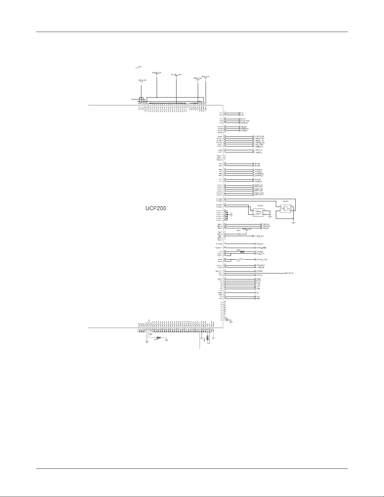
UCP200
1 2 3 4 5 6 7 8 9 10111213141516171819
A
B
C
D
E
F
G
H
J
K
L
M
N
P
R
T
U
V
W
1 2 3 4 5 6 7 8 9 10111213141516171819
Level3Repair
A
B
C
D
E
F
G
H
J
K
L
M
N
P
R
T
U
V
W
8-38
SAMSUNG Proprietary-Contents may change without notice
This Document can not be used without Samsung's authorization
Page 39

Level3Repair
NC
:
UME200
12345678910
A
B
C
D
E
F
12345678910
A
B
C
D
E
F
8-39
SAMSUNG Proprietary-Contents may change without notice
This Document can not be used without Samsung's authorization
 Loading...