

SAMSUNG DVD_907K Service Manual Cover
DIGITAL VERSATILE DISC PLAYER
DVD-907K
DVD-808K
DVD-807K
DVD-9901A
SERVICE
1. Precautions
2. Reference Information
3. Product Specification
4. Operating Instructions
5. Disassembly and Reassembly
6. IC Descriptions
7. Circuit Descriptions
8. Troubleshooting
9. Exploded Views and Parts List
10. Packing Diagram
11. Electrical Parts List
12. Block Diagram
13. PCB Diagrams
14. Wiring Diagram
15. Schematic Diagrams
Manual
DIGITAL VERSATILE DISC PLAYER CONTENTS
SERVICE MANUAL DVD-907K/808K/807K/DVD-9901A
ELECTRONICS
© Samsung Electronics Co., Ltd. MAR. 1999
Printed in Korea
AH68-00089A
Samsung Electronics 1-1
1. Before returning an instrument to the customer,
always make a safety check of the entire instrument, including, but not limited to, the following
items:
(1) Be sure that no built-in protective devices are
defective or have been defeated during servicing.
(1)Protective shields are provided to protect both
the technician and the customer. Correctly replace
all missing protective shields, including any remove
for servicing convenience. (2) When reinstalling the
chassis and/or other assembly in the cabinet, be
sure to put back in place all protective devices,
including, but not limited to, nonmetallic control
knobs, insulating fishpapers, adjustment and
compartment covers/shields, and isolation resistor/capacitor networks. Do not operate this instrument or permit it to be operated without all protective devices correctly installed and functioning.
(2) Be sure that there are no cabinet openings
throught which adults or children might be able to
insert their fingers and contact a hazardous voltage. Such openings include, but are not limited to,
excessively wide cabinet ventilation slots, and an
improperly fitted and/or incorrectly secured cabinet
back cover.
(3) Leakage Current Hot Check-With the instrument
completely reassembled, plug the AC line cord
directly into a 120V AC outlet. (Do not use a isolation transformer during this test.) Use a leakage
current tester or a metering system that complies
with American National Standards institute(ANSI)
C101.1 Leakage Current for Appliances and
Underwriters Laboratories (UL) 1270 (40.7). With
the instrument’s AC switch first in the ON position
and then in the OFF position, measure from a
known earth ground (metal waterpipe, conduit, etc.)
to all exposed metal parts of the instrument (antennas, handle brackets, metal cabinets, screwheads,
metallic overlays, control shafts, etc.), especially
any exposed metal parts that offer an electrical
return path to the chassis.
Any current measured must not exceed 0.5 millamp. Reverse the instrument power cord plug in
the outlet and repeat the test. See Figure 1-1.
Fig. 1-1 AC Leakage Test
Any measurements not within the limits specified
herein indicate a potential shock hazard that must
be ellminated before returning the instrument to the
customer.
(4) Insulation Resistance Test Cold Check-(1) Unplug
the power supply cord and connect a jumper wire
between the two prongs of the plug. (2) Turn on
the power switch of the instrument. (3) Measure
the resistance with an ohmmeter between the
jumpered AC plug and all exposed metallic cabinet
parts on the instrument, such as screwheads,
antenna, control shafts, handle brackets, etc. When
an exposed metallic part has a return path to the
chassis, the reading should be between 1 and 5.2
megohm. When there is no return path to the chassis, the reading must be infinite. If the reading is not
within the limits specified, there is the possibility of
a shock hazard, and the instrument must be
repared and rechecked before it is returned to the
customer. See figure 1-2.
Device
Under
Test
(Reading should
not be above
0.5mA)
Leakage
Current
Tester
Earth
Ground
Test all
exposed metal
surfaces
Also test with
plug reversed
(using AC adapter
plug as required)
2-Wire Cord
1. Pre cautions
1-1 Safety Precautions
Precautions
1-2 Samsung Electronics
Fig.1-2 Insulation Resistance Test
2. Read and comply with all caution and safety related
notes non or inside the cabinet, or on the chassis.
3. Design Afteration Warning-Do not alter of add to the
mechanical or electrical design of this instrument.
Design alterations and additions, including but not
limited to, circuit modifications and the addition of
items such as auxiliary audio output connections,
might alter the safety characteristics of this instrument and create a hazard to the user. Any design
alterations or additions will make you, the servicer,
responsible for personal injury or property damage
resulting therefrom.
4. Observe original lead dress. Take extra care to
assure correct lead dress in the following areas:(1)
near sharp edges, (2) near thermally hot parts (be
sure that leads and components do not touch thermally hot parts), (3) the AC supply, (4) high voltage,
and (5) antenna wiring. Always inspect in all areas
for pinched, out-of-place, or frayed wiring, Do not
change spacing between a componect and the
printed-circuit board. Check the AC power cord for
damage.
5. Components, parts, and/or wiring that appear to
have overheated or that are otherwise damaged
should be replaced with components, parts and/or
wiring that meet original specifications. Additionally,
determine the cause of overheating and/or damage
and, if necessary, take corrective action to remove
any potential safety hazard.
6. Product Safety Notice-Some electrical and mechanical parts have special safety-related characteristics
which are often not evident from visual inspection,
nor can the protection they give necessarily be
obtained by replacing them with components rated
for higher voltage, wattage, etc. Parts that have
special safety characteristics are identified by shading, an ( x )or a ( )on schematisc and parts lists.
Use of a substitute replacement that does not have
the same safety characteristics as the recommended replacement part might created shock, fire
and/or other hazards. Product safety is under
review continuously and new instructions are
issued whenever appropriate.
Antenna
Terminal
Exposed
Melal Part
ohm
ohmmeter

Samsung Electronics 1-3
CAUTION: Before servicing Instruments covered by
this service manual and its supplements, read and follow the Safety Precautions section of this manual.
Note: If unforseen circument create conflict between
the following servicing precautions and any of the
safety precautions, always follow the safety precautions. Remember: Safety First.
1-2-1 General Servicing Precautions
(1) a. Always unplug the instrument’s AC power cord
from the AC power source before (1) removing
or reinstalling any component, circuit board,
module or any other instrument assembly, (2)
disconnecting any instrument electrical plug or
other electrical connection, (3) connecting a test
substitute in parallel with an electrolytic capacitor in the instrument.
b. Do not defeat any plug/socker B+ voltage inter-
locks with which instruments covered by this
service manual might be equipped.
c. Do not apply AC power to this instrument and/or
any of its electrical assemblies unless all solidstate device heat sinks are correctly installed.
d. Always connect a test instrument’s ground lead
to the instrument chassis ground before connecting the test instrument positive lead. Always
remove the test instrument ground lead last.
Note: Refer to the Safety Precautions section ground
lead last.
(2) The service precautions are indicated or printed on
the cabinet, chassis or components. When servicing, follow the printed or indicated service precautions and service materials.
(3) The components used in the unit have a specified
flame resistance and dielectric strength. When
replacing components, use components which
have the same retings. Components identified by
shading, by( x ) or by ( ) in the circuit diagram
are important for safety or for the characteristics of
the unit. Always replace them with the exact
replacement components.
(4) An insulation tube or tape is sometimes used and
some components are raised above the printed wiling board for safety. The internal wiring is sometimes clamped to prevent contact with heating components. Install such elements as they were.
(5) After servicing, always check that the removed
screws, corponents, and wiring have been installed
correctly and that the portion around the serviced
part has not been damaged and so on. Further,
check the insulation between the blades of the
attachment plug and accessible conductive parts.
1-2-2 Insulation Checking Procedure
Disconnect the attachment plug from the AC outlet and
turn the power ON. Connect the insulation resistance
meter (500V) to the blades of the attachment plug. The
insulation resistance between each blade of the
attachment plug and accessible conductive parts(see
note) should be more than 1 Megohm.
Note: Accesible conductive parts include metal panels, input terminals, earphone jacks, etc.
1-2 Servicing Precautions

1-4 Samsung Electronics
Electrostatically Sensitive Devices (ESD)
Some semiconductor (solid state) devices can be
damaged easily by static electricity.
Such components commonly are called Electro statically Sensitive Devices(ESD). Examples of typical
ESD devices are integrated circuits and some fieldeffect transistors and semiconductor chip components.
The following techniques should be used to help
reduce the incidence of component damage caused
by static electricity.
(1) Immediately before handling any semiconductor
component or semiconductor-equipped assembly,
drain off any electrostatic aharge on your body by
touching a known earth ground. Alternatively,
obtain and wear a commercially available discharging wrist strap device, which should be
removed for potential shock reasons prior to applying power to the unit under test.
(2) After removing an electrical assembly equipped
with ESD devices, place the assembly on a conductive surface such as aluminum foil, to prevent
electrostatic charge buildup or exposure of the
assembly.
(3) Use only a grounded-tip soldering iron to solder or
unsolder ESD devices.
(4) Use ouly an anti-static solder removal devices.
Some solder removal devices not classified as
“anti-static” can generate electrical charges sufficient to damage ESD devices.
(5) Do not use freon-propelled chemicals. These can
generate electrical charges sufficient to damge
ESD devices.
(6) Do not remove a replacement ESD device from its
protective package until immediately before your
are ready to install it.(Most replacement ESD
devices are packaged with leads electrically shorted together by condutive foam, aluminum foil or
comparable conductive materials).
(7) Immediately before removing the protective mate-
rials from the leads of a replacement ESD device,
touch the protective material to the chassis or circuit assembly into which the device will be
installed.
CAUTION: Be sure no power is applied to the chassis
or circuit, and observe all other safety precautions.
(8) Minimize bodily motions when handling unpack-
aged replacement ESD devices. (Otherwise harmless motion such as the brushing together of your
clothes fabric or the lifting of your foot from a carpeted floor can generate static electrictity suffcient
to damage an ESD device).
1-3 ESD Precautions
Samsung Electronics 1-5
* The laser diode in the optical pick up may suffer elec-
trostatic breakdown because of potential static electricity from clothing and your body.
The following method is recommended.
(1) Place a conductive sheet on the work bench (The
black sheet used for wrapping repair parts.)
(2) Place the set on the conductive sheet so that the
chassis is grounded to the sheet.
(3) Place your hands on the conductive sheet(This
gives them the same ground as the sheet.)
(4) Romove the optical pick up block
(5) Perform work on top of the conductive sheet. Be
careful not to let your clothes or any other static
sources to touch the unit.
* Be sure to put on a wrist strap grounded to the
sheet.
* Be sure to lay a conductive sheet made of copper
etc. Which is grounded to the table.
Fig.1-3
(6) Short the short terminal on the PCB, which is inside
the Pick-Up ASS’Y, before replacing the Pick-Up.
(The short terminal is shorted when the Pick-Up
Ass’y is being lifted or moved.)
(7) After replacing the Pick-up, open the short terminal
on the PCB.
1-4 Handling the optical pick-up
THE UNIT
WRIST-STRAP
FOR GROUNDING
1M
1M
CONDUCTIVE SHEET
1-6 Samsung Electronics
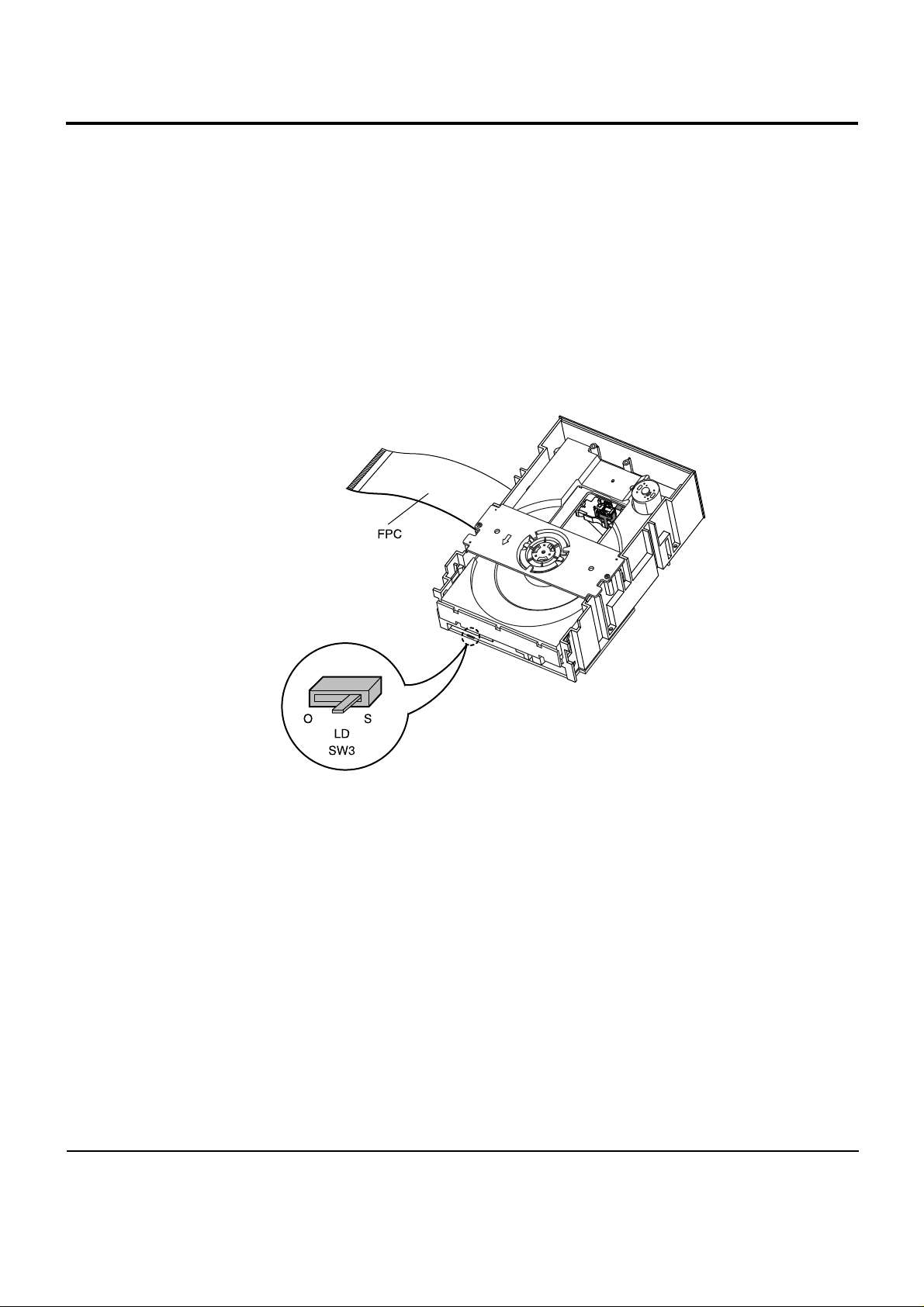
1-5-1 Disassembly
1) Remove the power cable.
2) Switch LD SW3 on deck PCB to ‘S’ before removing the FPC
( inserted into Main PCB CN1. See Fig 1-4.)
3) Disassemble the deck.
4) Disassemble the deck PCB.
5) Replace the Pick-up.
1-5-2 Assembly
1) Replace the Pick-up.
2) Assemble the deck PCB.
3) Reassemble the deck.
4) Switch LD SW3 on deck PCB to ‘O’ and insert
FPC into Main PCB CN1 (See Fig 1-4).
1-5 Pick-up disassembly and ressembly
Note : If the assembly and disassembly are not done in correct sequence, the Pick-up may be damaged.
Fig. 1-4
Samsung Electronics 2-1
2. Reference Information
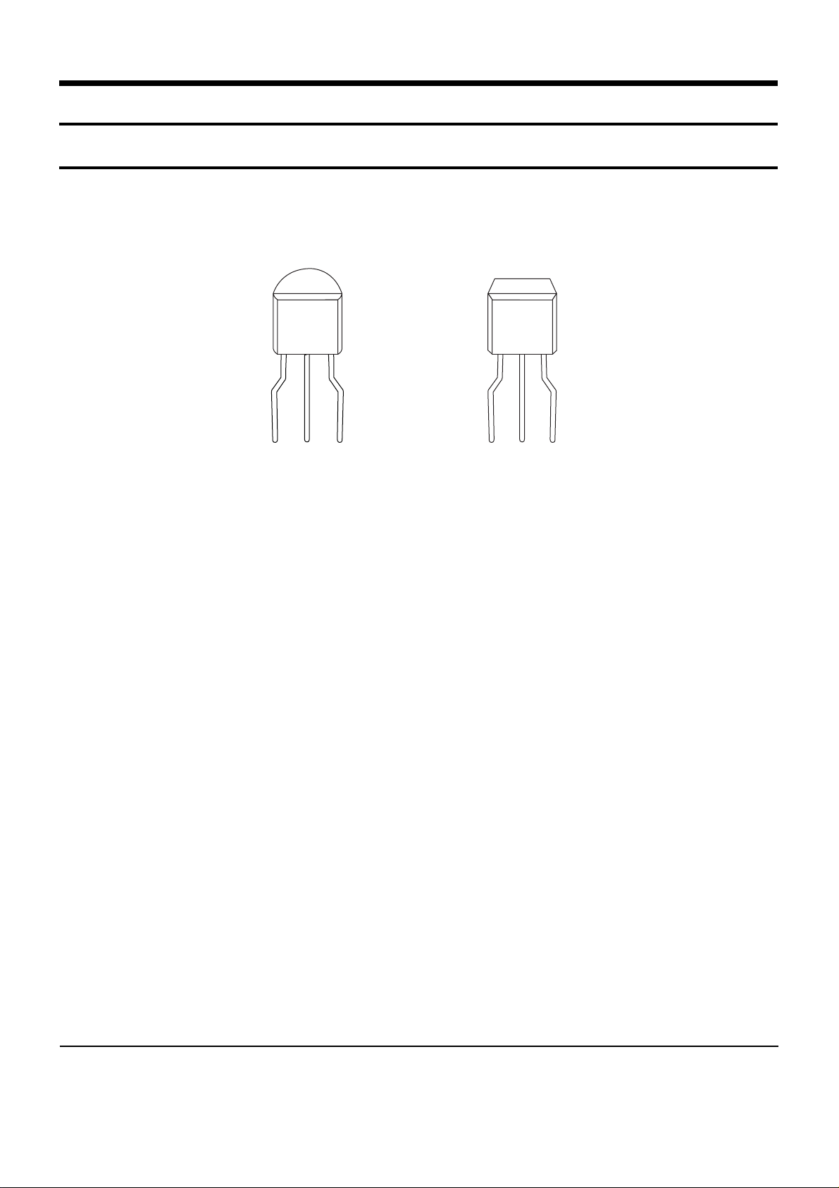
2-1 Semiconductor Base Diagram
Fig. 2-1
RQ1
SS9012
S9012
G-634
E B C
D G S
K184
Y 6A
SQ1
K184
2-2 Samsung Electronics
2-2 Chip Replacement
1) Do not touch the part body directly with the soldering iron. ICs, especially TSOP, are easily damaged by heat.
2) Use care regarding soldering iron tip and avoid
repidly heating parts. Some parts can be damaged
by sudden heating. Preheat the part at about
100°… for several minutes before installing it.
3) Use soldering tip temperature of about 240°… or
larger parts, use a slightly higher temperature
(about 280°…).
4) The thin(0.3mm)solder for miniature parts does
not contain adequate flux. Supplementary flux is
thus needed in most cases.
5) Use care not to damage the circuit pattern, especially when removing.
6) Because of the many pins, cleanliness of the pattern is extremely important after removing the IC.
7) Use care to avoid solder bridges. Remove any that
occurs.
8) Position the part carefully. They will also affect the
soldering operation. Be very precise in positioning
the IC. Soldering opposite pins first holds the IC in
place and makes soldering the other pins easier.
9) Do not reuse removed parts.
10) Check for solder joints, especially miniature parts
with small lead.
11) A defective trimming resistor cannot be adjusted
externally. Replace with an ordjnary variable resistor.
12) It is important to inspect the work with a magnifier.
Check after installing (cold solder joints, etc.).
2-2-1 Precaution for the chip Replacement
The tools for the chip replacement are as follows:
1) Thin tip type soldering iron
2) Small flat-blade tip-type soldering iron
3) Special desoldering tip iron
4) Airblower unit
5) Flat Package Pick-up
6) Flux can be cleaned by water
7) 0.3mm thin solder can be cleaned by water
8) Desoldering wire
9) Tweezers
2-2-2 Tools for the Chip Replacement
2-2-3 Chip Resistors and Chip Capacitors
-- Kind of the Part
The kind of chip resistors and chip capacitors as follows:d
1) Think Film Chip Resistors
2) Carbon Film Chip Resistors
3) Metal Film Chip Resistors
4) Chip Ceramic Capacitors
5) Chip Trimming Resistors
-- Removing the Part
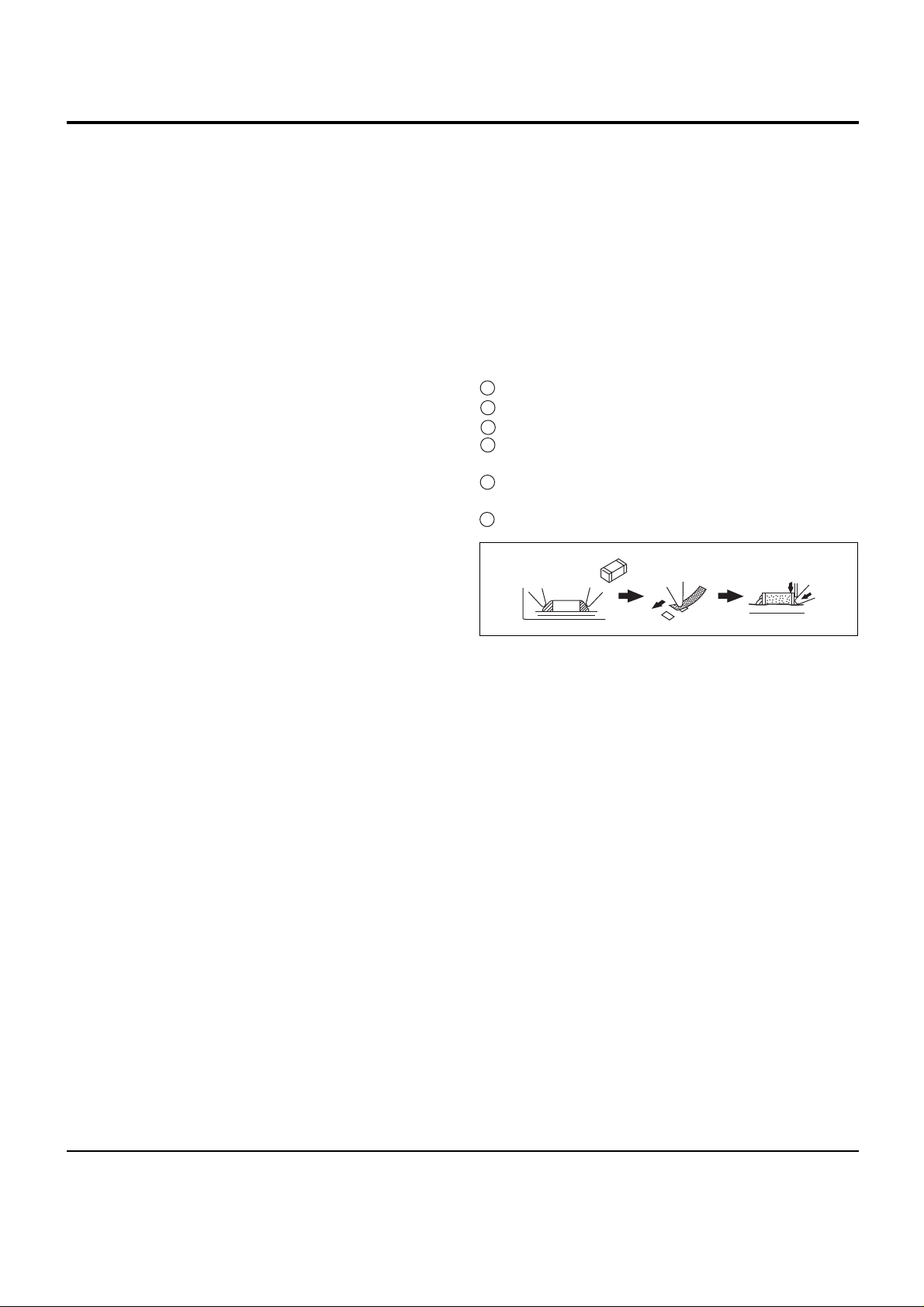
1) Using two soldering irons:
Use thin tip soldering irons.
Use soldering tip temperature of about 280°….
Simultaneously heat both ends of the part.
While heating, grasp the part with the tips of the
soldering irons and remove it.
Use desoldering wire to completely remove the old
solder from the part location of the board.
A clean pattern for installing the new part is very
important.
Fig 2-2
-- Installing the Part
1) Use desoldering wire to remove the previous solder.
2) Clean the location.
3) Apply flux.
4) Position the IC and solder two pins at opposite sides.
5) Use a sharp tipped soldering iron and carefully
solder each Pin.(After gaining experience, a thicker
tip can be used for better work efficiency.)
6) Remove any solder bridges with desoldering wire.
7) Inspect the work with a magnifier.
1
2
3
4
5
6
Precautions
Samsung Electronics 2-3
-- Kind of the Part
The kind of the part is as follows:
1) Chip VRs.
2) Chip Trimmer Capacitors
3) Diode
4) Transistors
-- Removing the Part
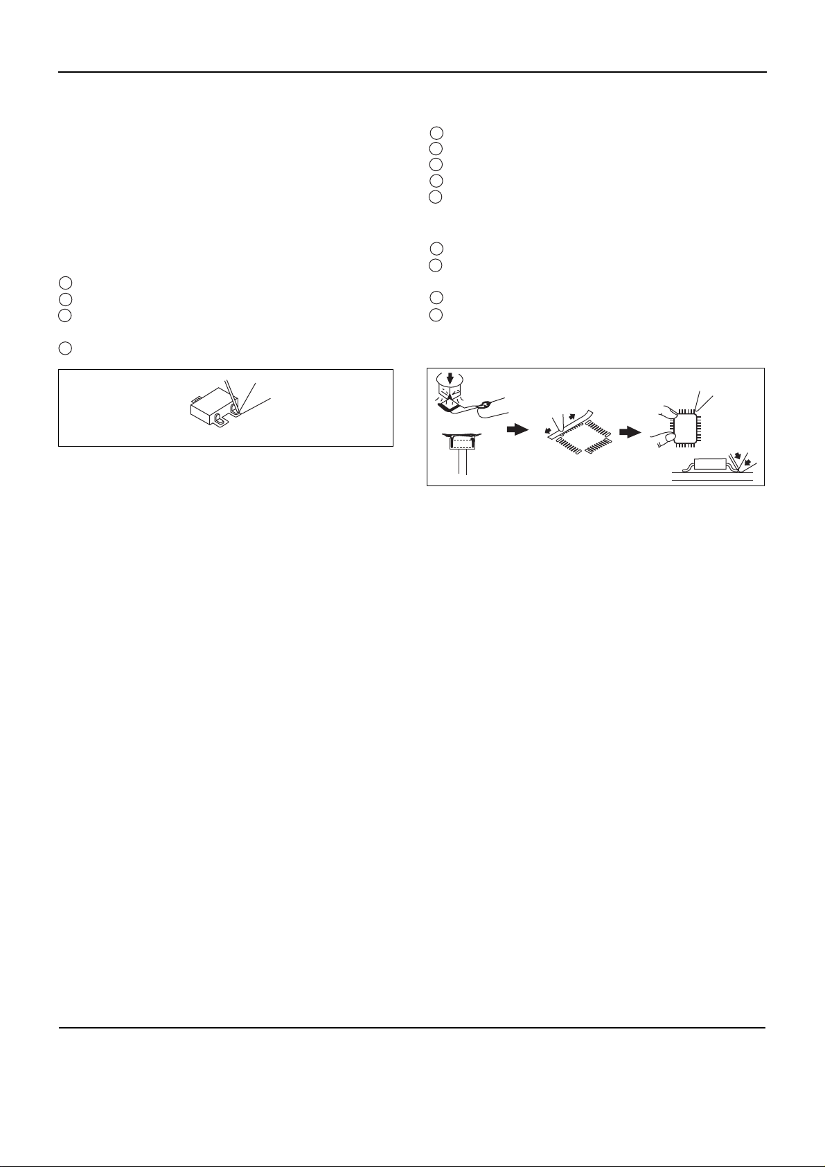
1) Using two soldering irons:
Use small flat-blade tips.
Heat the leads of the part simultaneously.
When the solder melts, grasp and remove the part
with the soldering iron tips.
Remove the old solder with desoldering wire.
2-2-4 Diodes and Tr.
-- The kind of the Chip ICs
The kind of the chip ICs are as follows:
1) SOP(Small Outline Package)IC
2) SSOP(Shrink Small Outline Package)IC
3) VSOP(Very Small Outline Package)IC
4) QFP(Quad Flat Package)IC
5) VQFP(Very Quad Flat Package)IC
6) PLCC(Plastic Leaded Chip Carrier)IC
7) TSOP(Thin Small Outline Package)IC
2-2-5 Chip ICs
-- Removing the Part
1) Using special desoldering iron:
Selet the tip according to the size and shape of the IC.
“Tin” the tip with a small amount of the IC leads.
Set the tip squarely over the IC leads.
When the solder melts, carefully twist the iron.
Raise and remove the IC.
2) Using shaped airblower unit:
Select the correct nozzle.
Select the temperature and airblow(suggested:
temperature:7, airblow:4)
Engage the IC removing tool.
Use the airblow to preheat the IC for about 5
seconds, then heat with the nozzle until the IC
remover lifts the part from the board.
IC
Fig 2-4
-- Installing the Part
1) Use desoldering wire to remove the previous solder.
2) Clean the location.
3) Apply flux.
4) Position the IC and solder two pins at opposite sides.
5) Use a sharp tipped soldering iron and carefully sol
der each Pin.(After gaining experience, a thicker tip
can be used for better work efficiency.)
6) Remove any solder bridges with desoldering wire.
7) Inspect the work with a magnifier.
Fig 2-3
-- Installing the Part
1) Clean the area where the new part is to be mounted.
2) Apply flux.
3) Set part correctly into position, prevent it from shifting.
4) Use sharp soldering iron tip. Bring close to the
part contact without actually touching it. Melt thin
solder between the tip and part si that it flows into
the part contact.
1
234
123
45123
4

Precautions
2-4 Samsung Electronics
MEMO
Samsung Electronics 6-1
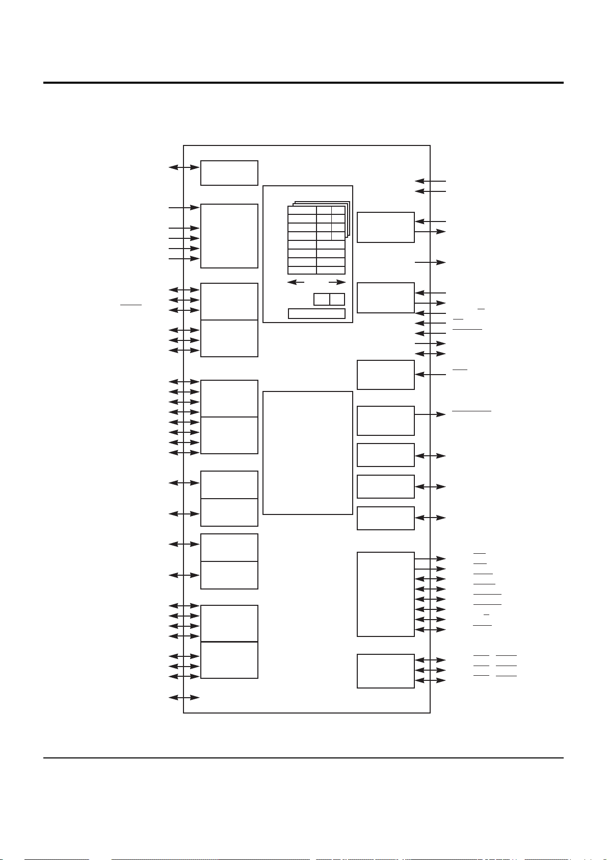
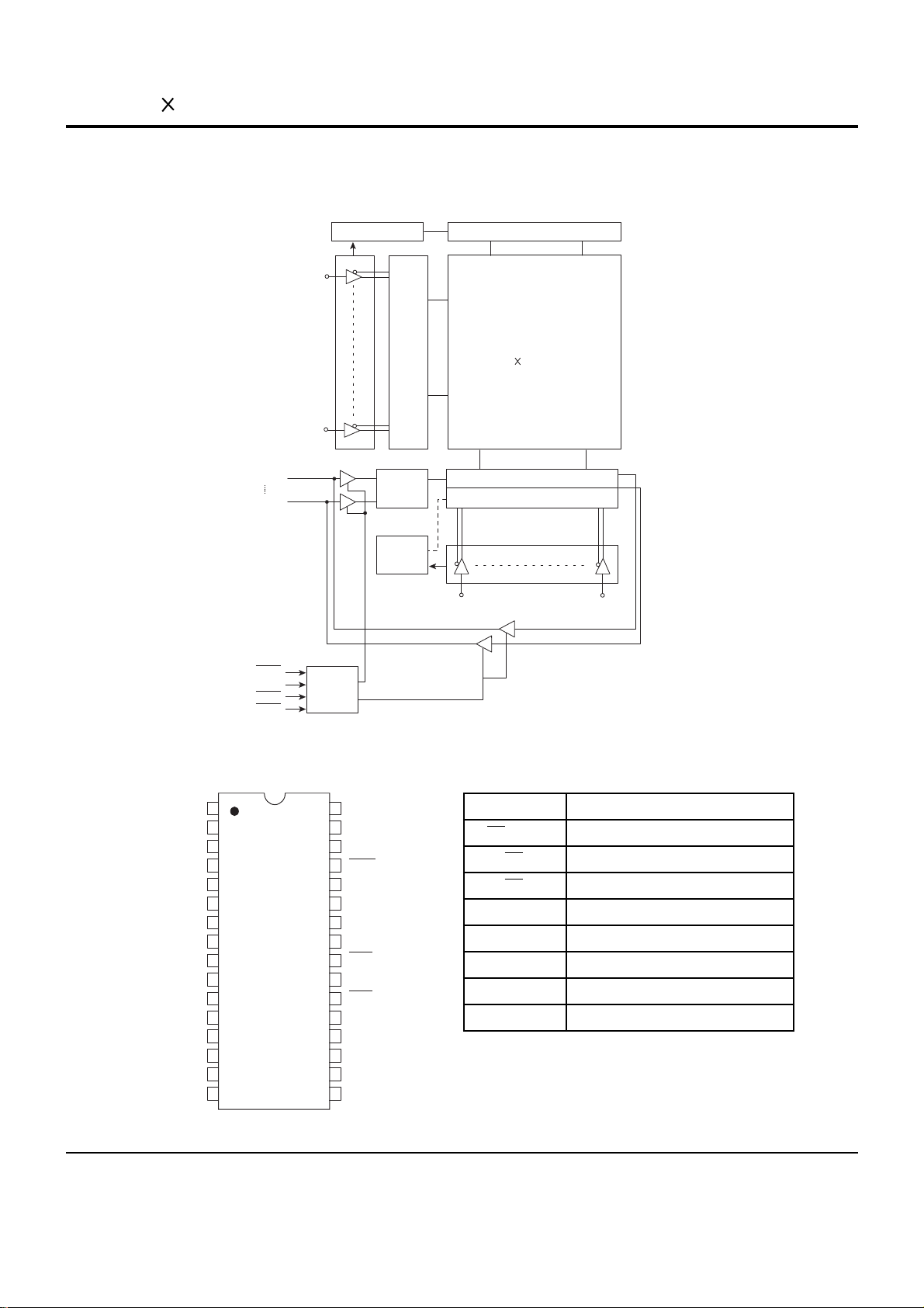
6. IC Descriptions
List
6-1
6-2
6-3
6-4
6-5
6-6
6-7
6-8
15-1-3 Data Processor
15-1-1 Micom
MIC1
MIC2
TMP93CS41
MAIN MICOM
4Megabit(512K 8-bit) CMOS EPROM
128K 8 bit CMOS SRAM
RF IC
DPD IC
3-PHASE MOTOR DRIVER
SERVO & CD DATA PROCESSOR
DVD DATA PROCESSOR
512K 8 bit CMOS DRAM
AUDIO/VIDEO DECODER
EPROM
CMOS DRAM
DIGIT AL-TO ANALOG CONVERTER
DIGIT AL-TO ANALOG CONVERTER
DIGITAL VIDEO ENCODER
FRONT MICOM
ECHO SOUND PROCESSOR
Am27C040
KM681000
TA1236F
TA1253F
BA6840
TC9420F
TC90A19F
KM48C512
ZiVA D6-L
AM27C4096
KM416C254DJ
AK4324
PCM1720
PCM1723
SAA7128
LC86P6232
ES56033
MIC3
RIC1
RIC2
SIC5
SIC7
DIC1
DIC2
BIC1
BIC2
AIC1
AIC2
AIC3
VIC1
FIC1
KIC1
15-1-2 Servo
15-1-4 A/V Decoder
15-1-5 Audio
15-1-6 Video
15-2 Front Board
15-4 Karaoke Board
6-9
6-10
6-11
6-12
BIC3,BIC4,BIC5,BIC6,BIC7
6-13
6-14
6-15
DIGITAL-TO ANALOG CONVERTER WITH PLL
6-16
6-17
6-18
SCHEMATIC
LOCATION DEVICE FUNCTION
6-2 Samsung Electronics
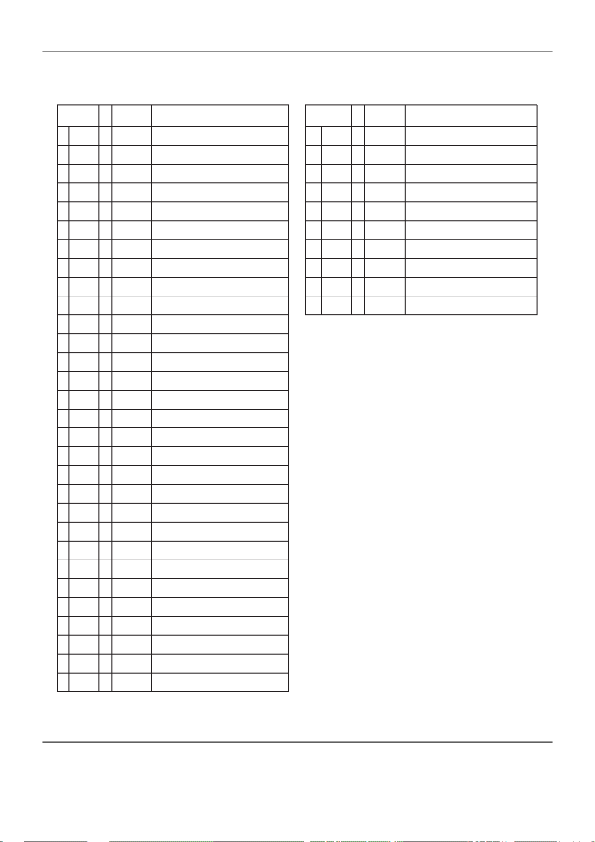
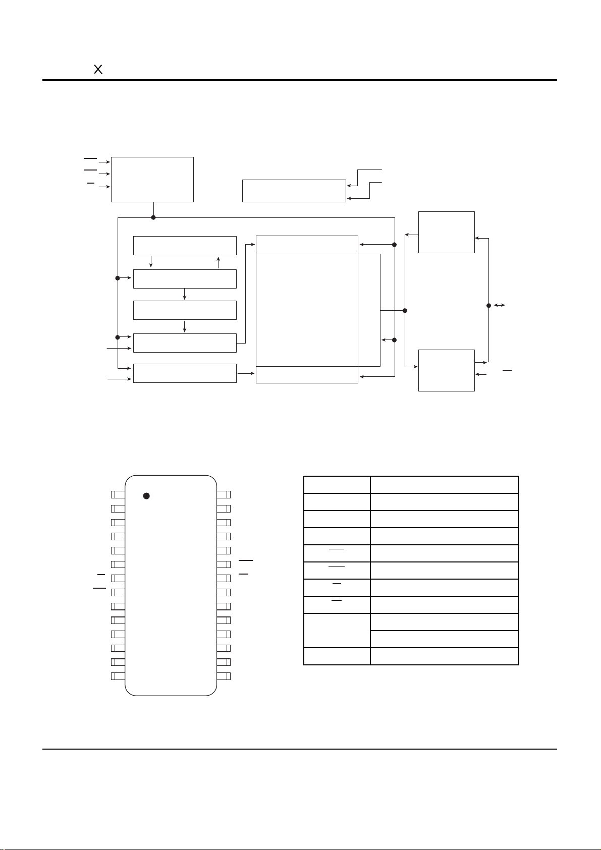
6-1 MAIN MICOM (MIC1 : TMP93CS41)
PAO~PA6
PA7(SCOUT)
P50 to P57
(ANO to AN7)
AVCC
AVSS
VREFH
VREFL
(TXD0)P90
(RXD0)P91
(SCLK0/CTS0)P92
(TXD1)P93
(RXD1)P94
(SCLK1)P95
(PG 00)P60
(PG 01)P61
(PG 02)P62
(PG 03)P63
(PG 10)P64
(PG 11)P65
(PG 12)P66
(PG 13)P67
(T10)P70
(T01)P71
(T02)P72
(T03)P73
(INT4/T14)P80
(INT5/T15)P81
(T04)P82
(T05)P83
(INT6/T16)P84
(INT7/T17)P85
(T06)P86
(INTO)P87
VCC[3]
VSS[3]
X1
X2
CLK
XT1
XT2
AM8/16
EA
RESET
ALE
TEST2,1
NMI
WDTOUT
P00 to P07
(AD0 to AC7)
P10 to P17
(AD8 to AD15/A8 toA15
P20 to P27
(A0 to A7/A16 to A23)
P30(RD)
P31(WR)
P32(HWR)
P33(WAIT)
P34(BUSRQ)
P35(BUSAK)
P36(R/W)
P37(RAS)
P40(CS0/CAS0)
P41(CS1/CAS1)
P42(CX2/CAS2)
cPORT A
High
Frequency
OSC
Low
Frequency
OSC
INTERRUPT
CONTROLLER
WATCH-DOG
TIMER
PORT 0
PORT 2
PORT 3
CS/WAIT
CONTROLLER
(3-BLOCK)
PORT 1
10-BIT 8CH
A/D
CONVERTER
SERIAL I/O
(CH,0)
SERIAL I/O
(CH,1)
PATTERN
GENERATOR
(CH,0)
PATTERN
GENERATOR
(CH,1)
16BIT TIMER
(TIMER 4)
16BIT TIMER
(TIMER 5)
8BIT TIMER
(TIMER 0)
8BIT TIMER
(TIMER 1)
8BIT PWM
(TIMER 2)
8BIT PWM
(TIMER 3)
900L-CPU
2KB RAM
XWA
XBC
ADE
XHL
XIX
XIY
XIZ
XSP
W
B
D
H
IX
IY
IZ
SP
A
C
E
L
32bit
FSR
P C
BLOCK DIAGRAM

IC Descriptions
6-3Samsung Electronics
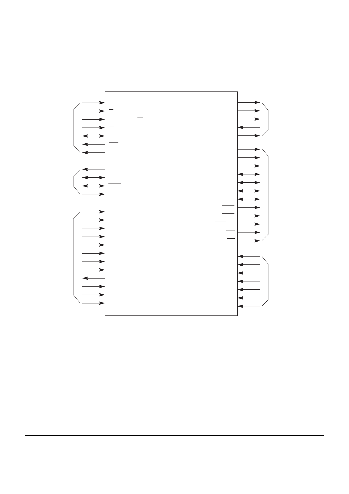
PIN ASSIGNMENT
IC Descriptions
6-4 Samsung Electronics
VSS
VCC
A16
A17
A18
A19
A20
A21
A22
A23
/RD
/WR
ML0/DIF0
WAIT
/BUSRQ
/BUSAK
ED_K
ED_T
/CS0
/CS1
/CS2
DVD_SEL
OPEN
CLOSE
S/D_SEL
SDA
SCL
BASS
SLEDGS
WDTO
V
SS
V
CC
A16
A17
A18
A19
A20
A21
A22
A23
P30
P31
P32
P33
P34
P35
P36
P37
P40
P41
P42
P60
P61
P62
P63
P64
P65
P66
P67
61
62
63
64
65
66
67
68
69
70
71
72
73
74
75
76
77
78
79
80
81
82
83
84
85
86
87
88
89
90
I/O
O
O
O
O
O
O
O
O
O
O
O
I
I
O
O
O
O
O
O
O
O
O
O
O
O
O
O
GND(0V)
+5V
Address Bus 16
Address Bus 17
Address Bus 18
Address Bus 20
Address Bus 21
Address Bus 22
Address Bus 23
Strobe for Reading External Momory
Strobe for Writing Data AD0 to AD7
Audio DAC Data Latch 0
/AKM4324 Control(“L”=16/24bit, “H”=20bit)
Address Bus 19
Request CPU Bus Wait
Bus Request
Bus Acknowledge
EEPROM Trans. Clock(I2S)
EEPROM Trans. Data(I2S)
Chip Select 0
Chip Select 1
Chip Select 2
DVD/CD Mode Control(DVD=”Low”)
Door Open Motor Control
Door Close Motor Control
Single/Dual Disc Select(Single=”Low”)
Video Encoder Trans. Data(l
2
C)
Video Encoder Trans. Clock(l
2
C)
Bass Redirection Control(“L”=SW On, “H”=SW Off)
Sled Gain Select
FUNCTION
PIN I/O NAME
FUNCTION
PIN I/O NAME
VSS
FEI
SPFG
/SECAM
/PAL
/NTSC
OP-SW
CL-SW
VREFH
V
SS
P50
P51
P52
P53
P54
P55
P56
P57
VREFH
91
92
93
94
95
96
97
98
99
100
I
I
I
I
I
I
I
I
I
GND
Focus Error Input
Spindle FG Input
SECAM=”H”
PAL =”H”
NTSC=”H”
Door Open SW
Door Close SW
Reference Voltage Input to A/DC(¡ H¡–)
PIN ASSIGNMENT
6-5Samsung Electronics
6-2 4Megabit (512K, 144 x 8-bit) CMOS EPROM (MIC2 ; Am27C040)
NAME
A0-A17
CE (E)
DQ0-DQ7
OE (G)
PGM (P)
Vcc
Vpp
Vss
1
2
3
4
5
6
7
8
9
10
11
12
13
14
15
16
Vpp
A16
A15
A12
A7
A6
A5
A4
A3
A2
A1
A0
DQ0
DQ1
DQ2
Vss
Vcc
PGM (P)
A17
A14
A13
A8
A9
A11
OE (G)
A10
CE (E)
DQ7
DQ6
DQ4
DQ4
DQ3
32
31
30
29
28
27
26
25
24
23
22
21
20
19
18
17
TOP VIEW
Output Enable
Chip Enable and
Prog Logic
Output Buffers
Y
Gating
2,097,152-Bit
Cell Matrix
Y
Decoder
A0-A17
Address
Inputs
OE
.
.
.
.
.
.
.
X
Decoder
Data Outputs
DQ0-DQ7
CE
Vpp
Vcc
Vss
CE/PCM
BLOCK DIAGRAM
FUNCTION
Address Inputs
Chip Enable Input
Data Input/Outputs
Output Enable Input
Program Enable Input
Vcc Syply Voltage
Program Voltage Input
Ground
PIN ASSIGNMENT
CE/PGM
8
4,194,304-Bit
CE (E)/PGM (P)
A18
18
CE (E)/PGM (P)
Chip Enable/Program Enable Input
6-6 Samsung Electronics
6-3 128K 8 bit CMOS SRAM (MIC3 ; KM681000B)
BLOCK DIAGRAM
Clk gen
Row
select
Data
cont
I/O
1
I/O8
CS1
CS2
WE
OE
I/O Circuit
Column select
A0 A1 A2 A3 A8 A9 A10 A11
Data
cont
Control
logic
Precharge circuit
Memory array
512 rows
256 8 columns
A4
A5
A6
A7
A12
A13
A14
A15
A16
1
2
3
4
5
6
7
8
9
10
11
12
13
14
15
16
17
18
19
20
21
22
23
24
25
26
27
28
29
30
31
32
32-DIP
32-SOP
N.C
A16
A14
A12
A7
A6
A5
A4
A3
A2
A1
A0
I/O1
I/O2
I/O3
VSS
VCC
A15
CS2
WE
A13
A8
A9
A11
OE
A10
CS1
I/O7
I/O8
I/O6
I/O5
I/O4
TOP VIEW PIN ASSIGNMENT
NAME
CS
1, CS2
FUNCTION
Chip Select Inputs
OE
Output Enable Input
WE
Write Enable Input
A0 ~ A16
Address Inputs
I/O1 ~ I/O8
Data Inputs/Outputs
Vcc
Power
Vss
Ground
N.C
No Connection

6-7Samsung Electronics
6-4 RF IC (RIC1 ; TA1236F)
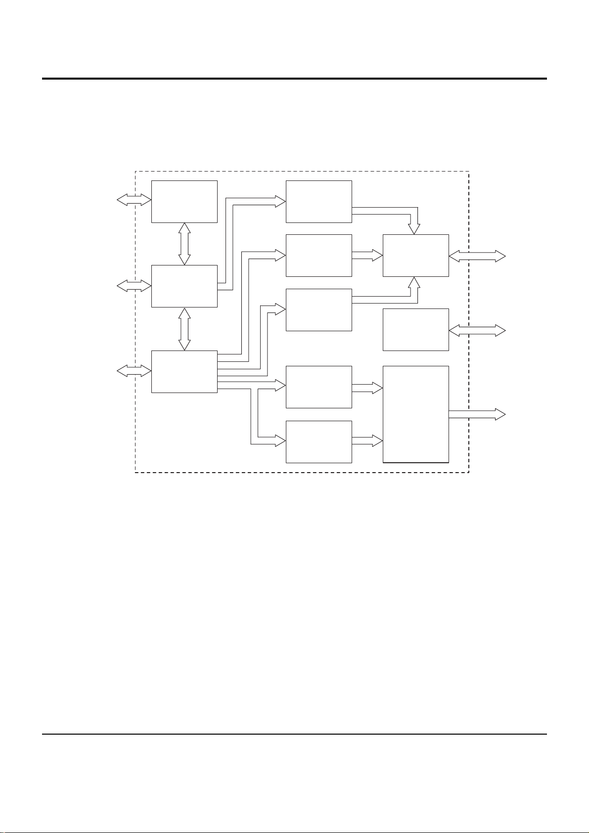
BLOCK DIAGRAM
IC Descriptions
6-8 Samsung Electronics
LOGIC DIAGRAM
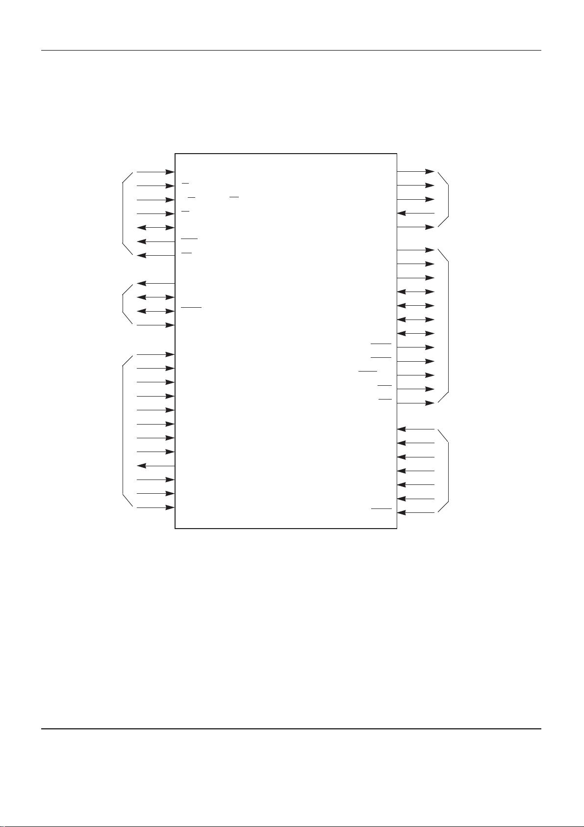
HADDR[2:0]
CS
R/W (M Mode)/WR (I Mode)
RD (I Mode)
HDATA[7:0]
WAIT
INT
Host
Interface
Signals
Video
Interface
Signals
DVD/CD
Interface
Signals
Audio
Interface
Signals
DRAM/ROM
Interface
Signals
Global
Interface
Signals
DA-DATA[2:0]
*
DA-LRCK
DA-BCK
DA-XCK
IEC958
MADDR[8:0]/MROMA[8:0]
MADDRH4
MADDRH1
MDATA[31:0]
MDATA[47:32]/MROMDATA[15:0]
MDATA[60:48]/MROMA[21:9]
MDATA[63:61]
MRAS1
MRAS0
MCAS[1:0]
MWE
MCE
SYSCLK
VDD
VSS
A_VSS
A_VDD
VDD5MAX
RESET
VDATA[7:0]
HSYNC
VSYNC
VCK
DVD-DATA[0]/CD-DATA
DVD-DATA[1]/CD-LRCK
DVD-DATA[2]/CD-BCK
DVD-DATA[3]/CD-C2PO
DVD-DATA[4]
DVD-DATA[5]
DVD-DATA[6]
DVD-DATA[7]
REQUEST
CSTROBE
ERROR
DACK
6-9Samsung Electronics
6-5 DPD IC (RIC2 ; TA1253F)
AGND
BIN1
N.C.
VREF
CIN1
N.C.
IREF
DIN1
DSEL
PDFIL1
PDFIL2
DVCC
DGND
TEOUT
DEFECT
TEST2
BDDC
TEST1
ACDC
BACTL
DPCTL
N.C.
AIN1
AVCC
1
2
3
4
5
6
7
8
9
10
11
12
13
14
15
16
17
18
19
20
21
22
23
24
NAME FUNCTION
Ground
Four division detector B inpt
No connection
Reference voltage input
Four division detector C input
No connection
Current source setting current input for phase
difference current conversion
Four division detector D input
Phase difference signal off-set compensation
polarity selection input
Phase difference current voltage time constant
setting external capacitor
Phase difference current voltage time constant
setting external capacitor
Power (+5V) input
Grond
Tracking error signal ouput
Mute control input
For test
BD channel HPF time constant setting external
capacitor
For test
AC channel HPF time constant Setting external
capacitor
Tracking error balance control input
Phase difference signal off-set compensation
control input
No Connection
Four division detector A input
Power (+5V) input
PIN
PIN ASSIGNMENT
6-10 Samsung Electronics
6-6 3-PHASE MOTOR DRIVER (SIC5 ; BA6840 BFP)
BLOCK DIAGRAM
PIN ASSIGNMENT
NAME
Pin
FIN
3
4
5
6
7
9
10
13
14
15
16
17
20
GND
FUNCTION
Ground pin
A
3
Output pin
A
2
Output pin
Rnl
Current detector output pin
A
1
Output pin
GND
Ground pin
H1+
Hall signal input pin
H1-
Hall signal input pin
H2+
Hall signal input pin
H2-
Hall signal input pin
H3+
Hall signal input pin
H3-
Hall signal input pin
V
H
Hall bias pin
C
NF
Capacitor for phase compensation connection pin
NAME
Pin
21
22
23
24
25
26
E
CR
FUNCTION
Standard output current control pin
E
C
Output current control pin
ST/SP
Start/stop switch pin
REV
Reverse pin
V
cc
Power supply pin
V
M
Motor power supply pin

6-11Samsung Electronics
6-7 SERVO & CD DATA PROCESSOR (SIC7 ; TC9420F)
BLOCK DIAGRAM

IC Descriptions
6-12 Samsung Electronics
PIN ASSIGNMENT
IC Descriptions
6-13Samsung Electronics
IO2(DMOP)
IO2(DMON)
/DMOUT
/CKSE
/DACT
TESIN
TESIO1
V
SS
PXI
PXO
V
DD
XVSS
XI
XO
XV
DD
DVDO
RO
DV
SS
DVR
LO
DV
DD
TEST1
TEST2
TEST3
BUS0
66
67
68
69
70
71
72
73
74
75
76
77
78
79
80
81
82
83
84
85
86
87
88
89
90
Wide use I/O port
Wide use I/O port
Mode setting to output binary PWM signals of field
equalizer from IO0 and IO1 terminals and of disc
equalizer from IO2 and IO3 terminals
X¡fltal selection
DAC test mode
Test input (external VCO clock input)
Test I/O
Digital ground
DPS system clock oscillation circuit input
DPS system clock oscillation circuit output
Digital + power supply
Ground for system clock oscillation circuit
System clock oscillation circuit input
System clock oscillation circuit output
+ power supply for system clock oscillation
circuit
D/A converting section power supply
R channel data forward rotation output
D/A converting section ground
D/A converting section reference voltage
L channel data forward rotation output
D/A converting section power supply
Test mode terminal
Test mode terminal
Test mode terminal
Data I/O (for microcomputer interface)
BUS1
BUS2
BUS3
V
DD
V
SS
BUCK
/CCE
TEST4
/TSMOD
/RST
91
92
93
94
95
96
97
98
99
100
Chip enable signal input for microcomputer
interface
Data I/O (for microcomputer interface)
Data I/O (for microcomputer interface)
Data I/O (for microcomputer interface)
Digital + power supply
Digital ground
Clock input for microcomputer interface
Test mode terminal
Local test mode selection
Reset signal input
NAME FUNCTION
PIN
NAME FUNCTION
PIN
PIN ASSIGNMENT

6-14 Samsung Electronics
6-8 DVD DATA PROCESSOR (DIC1 ; TC90A19F)
BLOCK DIAGRAM

IC Descriptions
6-15Samsung Electronics
PIN ASSIGNMENT
IC Descriptions
6-16 Samsung Electronics
PIN ASSIGNMENT
MA4
MA3
MA2
MA1
MA0
DV
SS2
DV
DD2
MD7
MD6
MD5
MD4
MD3
MD2
MD1
MD0
SD7
SD6
SD5
SD4
DV
SS1
DV
DD1
SD3
SD2
SD1
SD0
66
67
68
69
70
71
72
73
74
75
76
77
78
79
80
81
82
83
84
85
86
87
88
89
90
External RAM address bus output
External RAM address bus output
External RAM address bus output
External RAM address bus output
External RAM address bus output
Digital ground
Digital power supply
External RAM data bus I/O
External RAM data bus I/O
External RAM data bus I/O
External RAM data bus I/O
External RAM data bus I/O
External RAM data bus I/O
External RAM data bus I/O
External RAM data bus I/O
MPEG data output
MPEG data output
MPEG data output
MPEG data output
Digital ground
Digital power supply
MPEG data output
MPEG data output
MPEG data output
MPEG data output
SERR
SBGN
SENB
SDCK
DV
SS1
SREQ
RSTN
DV
DD1
STDA
STCK
Digital power supply
MPEG data reliability flag output
(data error:L)
MPEG output secter synchronous signal output
(secter top:L)
MPEG data effective flag output (effective:L)
MPEG data transfer clock output
Digital ground
MPEG data request flag input(request:L)
Hard reset input (reset:L)
Operation monitor data output
(Output is carried out in synchronization
with the falling edge of SDCK)
Operation monitor synchronous signal
output (data top bit:L)
91
92
93
94
95
96
97
98
99
100
NAME FUNCTION
PIN
NAME FUNCTION
PIN
6-17Samsung Electronics
6-9 512 8 bit CMOS DRAM (DIC2 ; KM48C 512D)
PIN ASSIGNMENT
NAME
A0 ~ A9
FUNCTION
Address Input
DQ0 ~ 7
Data In/Out
Vss
Ground
RAS
Row Address Strobe
CAS
Column Address Strobe
W
Read/Write Input
OE
Data Output Enable
Vcc
Power(+5V)
Power(+3.3V)
N.C
No Connection
RAS
OE
CAS
W
Control
Clocks
VBB Generator
Vcc
Vss
Data in
Buffer
Data out
Buffer
Row Decoder
Refresh Timer
Refresh Control
Refresh Counter
Row Address Buffer
Col. Address Buffer
A0 - A9
A0 - A8
Memory Array
524,288 x8
Cells
Column Decoder
Sense Amps & I/O
DQ0
to
DQ7
1 28
27
26
25
2
3
4
24
5
23
6
22
7
21
8
20
9
19
10
18
11
17
12
16
13
15
14
Vcc
Vcc Vss
Vss
DQ0 DQ7
DQ6
DQ5
DQ4
DQ1
DQ2
DQ3
N.C
W
RAS
A9
A0
A1
A2
A3
A8
A7
A6
A5
A4
CAS
OE
N.C
BLOCK DIAGRAM
TOP VIEW
6-18 Samsung Electronics
6-10 AUDIO/VIDEO DECODER (BIC1 ; ZiVA D6-L)
Memory
Controller
OSD
Decoder
Video
Mixer
Video
Interface
Audio
Interface
Sync
Generator
Subpicture
Decoder
MPEG
Video
Decoder
Dolby Digital
Audio
Decoder
MPEG
Audio
Decoder
Host
Interface
Control Logic
Program
Stream
Decoder
DRAM/
ROM
Interface
Host
Interface
DVD/CD
Interface
ZZii VV AA DD eeccoo dd eerr
BLOCK DIAGRAM
Digital Audio
and
IEC-958
Interface
IC Descriptions
6-19Samsung Electronics
LOGIC DIAGRAM
HADDR[2:0]
CS
R/W (M Mode)/WR (I Mode)
RD (I Mode)
HDATA[7:0]
WAIT
INT
Host
Interface
Signals
Video
Interface
Signals
DVD/CD
Interface
Signals
Audio
Interface
Signals
DRAM/ROM
Interface
Signals
Global
Interface
Signals
DA-DATA[2:0]
*
DA-LRCK
DA-BCK
DA-XCK
IEC958
MADDR[8:0]/MROMA[8:0]
MADDRH4
MADDRH1
MDATA[31:0]
MDATA[47:32]/MROMDATA[15:0]
MDATA[60:48]/MROMA[21:9]
MDATA[63:61]
MRAS1
MRAS0
MCAS[1:0]
MWE
MCE
SYSCLK
VDD
VSS
A_VSS
A_VDD
VDD5MAX
RESET
VDATA[7:0]
HSYNC
VSYNC
VCK
DVD-DATA[0]/CD-DATA
DVD-DATA[1]/CD-LRCK
DVD-DATA[2]/CD-BCK
DVD-DATA[3]/CD-C2PO
DVD-DATA[4]
DVD-DATA[5]
DVD-DATA[6]
DVD-DATA[7]
REQUEST
CSTROBE
ERROR
DACK
 Loading...