

SAMSUNG DVD_907 Service Manual Cover
DIGITAL VERSATILE DISC PLAYER
DVD-907/927
SERVICE
1. Precautions
2. Reference Information
3. Product Specification
4. Operating Instructions
5. Disassembly and Reassembly
6. IC Descriptions
7. Circuit Descriptions
8. Troubleshooting
9. Exploded Views and Parts List
10. Packing Diagram
11. Electrical Parts List
12. Block Diagram
13. PCB Diagrams
14. Wiring Diagram
15. Schematic Diagrams
Manual
DIGITAL VERSATILE DISC PLAYER CONTENTS
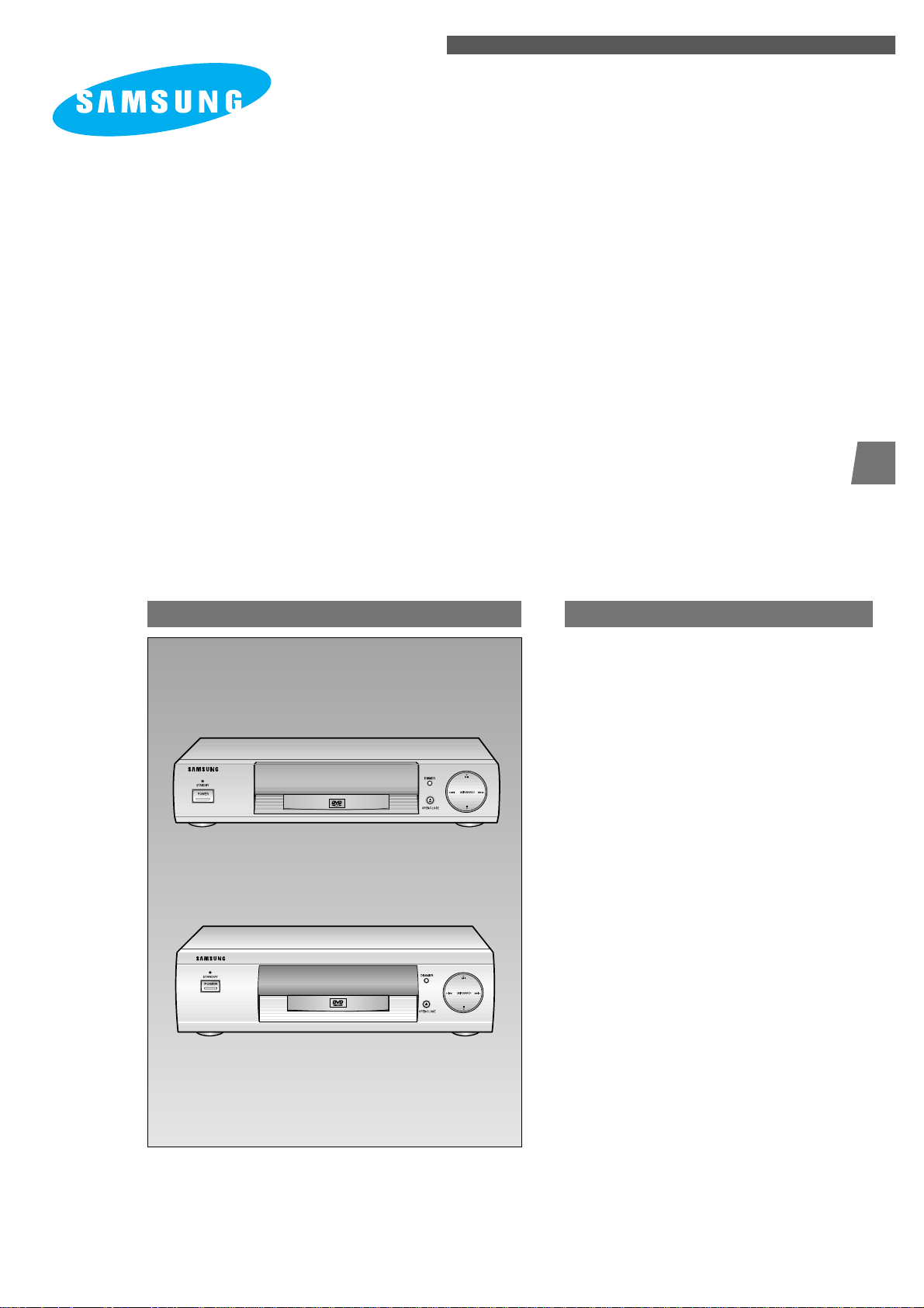
DVD-907
DVD-927

ELECTRONICS
© Samsung Electronics Co., Ltd. May. 1998
Printed in Korea
AH68-20198A
Samsung Electronics 1-1
1. Before returning an instrument to the customer,
always make a safety check of the entire instrument, including, but not limited to, the following
items:
(1) Be sure that no built-in protective devices are
defective or have been defeated during servicing.
(1)Protective shields are provided to protect both
the technician and the customer. Correctly replace
all missing protective shields, including any remove
for servicing convenience. (2) When reinstalling the
chassis and/or other assembly in the cabinet, be
sure to put back in place all protective devices,
including, but not limited to, nonmetallic control
knobs, insulating fishpapers, adjustment and
compartment covers/shields, and isolation resistor/capacitor networks. Do not operate this instrument or permit it to be operated without all protective devices correctly installed and functioning.
(2) Be sure that there are no cabinet openings
throught which adults or children might be able to
insert their fingers and contact a hazardous voltage. Such openings include, but are not limited to,
excessively wide cabinet ventilation slots, and an
improperly fitted and/or incorrectly secured cabinet
back cover.
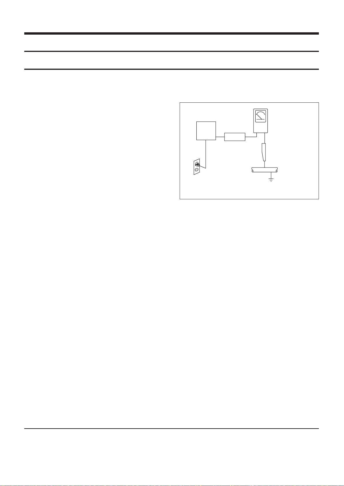
(3) Leakage Current Hot Check-With the instrument
completely reassembled, plug the AC line cord
directly into a 120V AC outlet. (Do not use a isolation transformer during this test.) Use a leakage
current tester or a metering system that complies
with American National Standards institute(ANSI)
C101.1 Leakage Current for Appliances and
Underwriters Laboratories (UL) 1270 (40.7). With
the instrument’s AC switch first in the ON position
and then in the OFF position, measure from a
known earth ground (metal waterpipe, conduit, etc.)
to all exposed metal parts of the instrument (antennas, handle brackets, metal cabinets, screwheads,
metallic overlays, control shafts, etc.), especially
any exposed metal parts that offer an electrical
return path to the chassis.
Any current measured must not exceed 0.5 millamp. Reverse the instrument power cord plug in
the outlet and repeat the test. See Figure 1-1.
Fig. 1-1 AC Leakage Test
Any measurements not within the limits specified
herein indicate a potential shock hazard that must
be ellminated before returning the instrument to the
customer.
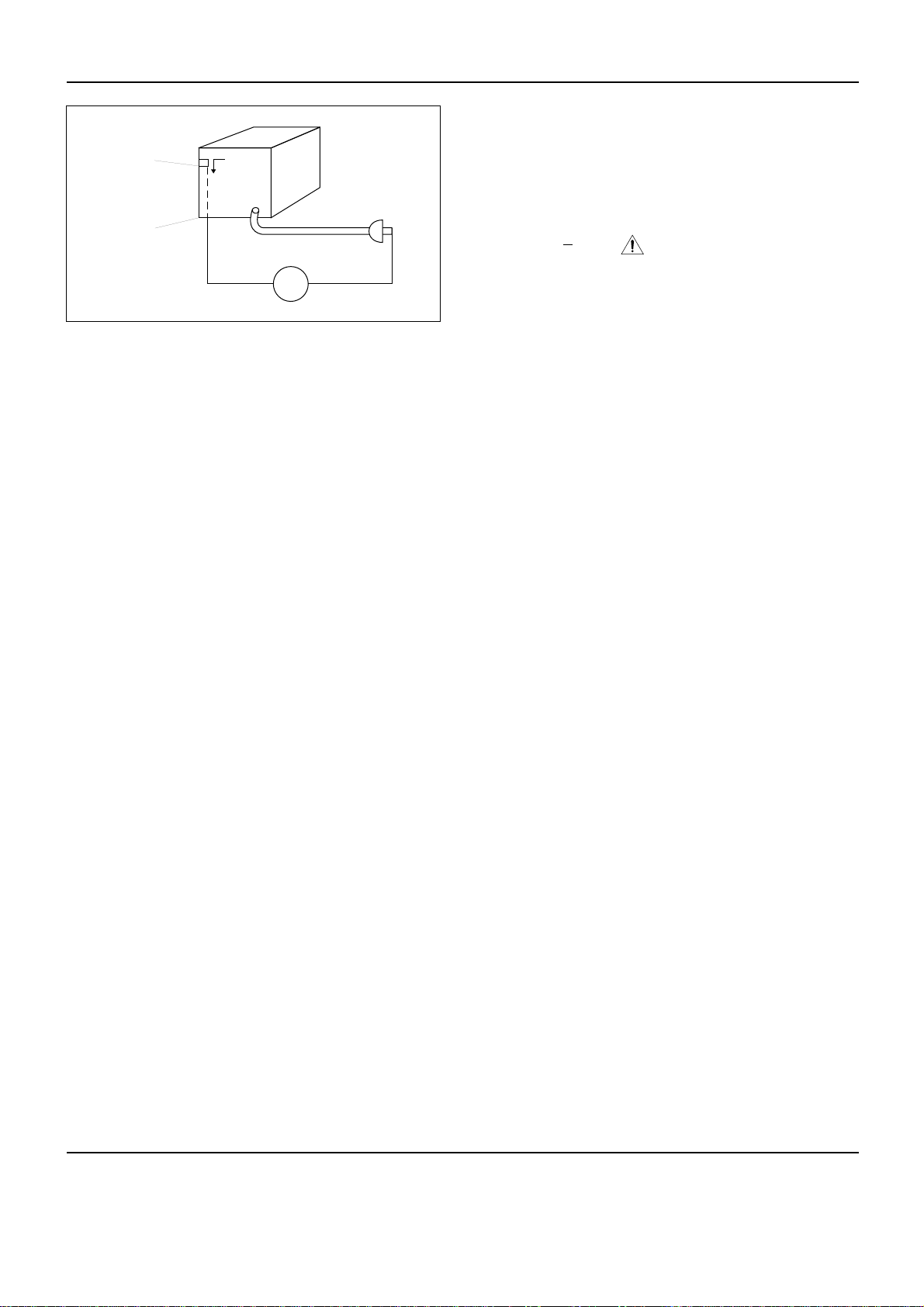
(4) Insulation Resistance Test Cold Check-(1) Unplug
the power supply cord and connect a jumper wire
between the two prongs of the plug. (2) Turn on
the power switch of the instrument. (3) Measure
the resistance with an ohmmeter between the
jumpered AC plug and all exposed metallic cabinet
parts on the instrument, such as screwheads,
antenna, control shafts, handle brackets, etc. When
an exposed metallic part has a return path to the
chassis, the reading should be between 1 and 5.2
megohm. When there is no return path to the chassis, the reading must be infinite. If the reading is not
within the limits specified, there is the possibility of
a shock hazard, and the instrument must be
repared and rechecked before it is returned to the
customer. See figure 1-2.
Device
Under
Test
(Reading should
not be above
0.5mA)
Leakage
Current
Tester
Earth
Ground
Test all
exposed metal
surfaces
Also test with
plug reversed
(using AC adapter
plug as required)
2-Wire Cord
1. Pre cautions
1-1 Safety Precautions
Precautions
1-2 Samsung Electronics
Fig.1-2 Insulation Resistance Test
2. Read and comply with all caution and safety related
notes non or inside the cabinet, or on the chassis.
3. Design Afteration Warning-Do not alter of add to the
mechanical or electrical design of this instrument.
Design alterations and additions, including but not
limited to, circuit modifications and the addition of
items such as auxiliary audio output connections,
might alter the safety characteristics of this instrument and create a hazard to the user. Any design
alterations or additions will make you, the servicer,
responsible for personal injury or property damage
resulting therefrom.
4. Observe original lead dress. Take extra care to
assure correct lead dress in the following areas:(1)
near sharp edges, (2) near thermally hot parts (be
sure that leads and components do not touch thermally hot parts), (3) the AC supply, (4) high voltage,
and (5) antenna wiring. Always inspect in all areas
for pinched, out-of-place, or frayed wiring, Do not
change spacing between a componect and the
printed-circuit board. Check the AC power cord for
damage.
5. Components, parts, and/or wiring that appear to
have overheated or that are otherwise damaged
should be replaced with components, parts and/or
wiring that meet original specifications. Additionally,
determine the cause of overheating and/or damage
and, if necessary, take corrective action to remove
any potential safety hazard.
6. Product Safety Notice-Some electrical and mechanical parts have special safety-related characteristics
which are often not evident from visual inspection,
nor can the protection they give necessarily be
obtained by replacing them with components rated
for higher voltage, wattage, etc. Parts that have
special safety characteristics are identified by shading, an ( x )or a ( )on schematisc and parts lists.
Use of a substitute replacement that does not have
the same safety characteristics as the recommended replacement part might created shock, fire
and/or other hazards. Product safety is under
review continuously and new instructions are
issued whenever appropriate.
Antenna
Terminal
Exposed
Melal Part
ohm
ohmmeter

Samsung Electronics 1-3
CAUTION: Before servicing Instruments covered by
this service manual and its supplements, read and follow the Safety Precautions section of this manual.
Note: If unforseen circument create conflict between
the following servicing precautions and any of the
safety precautions, always follow the safety precautions. Remember: Safety First.
1-2-1 General Servicing Precautions
(1) a. Always unplug the instrument’s AC power cord
from the AC power source before (1) removing
or reinstalling any component, circuit board,
module or any other instrument assembly, (2)
disconnecting any instrument electrical plug or
other electrical connection, (3) connecting a test
substitute in parallel with an electrolytic capacitor in the instrument.
b. Do not defeat any plug/socker B+ voltage inter-
locks with which instruments covered by this
service manual might be equipped.
c. Do not apply AC power to this instrument and/or
any of its electrical assemblies unless all solidstate device heat sinks are correctly installed.
d. Always connect a test instrument’s ground lead
to the instrument chassis ground before connecting the test instrument positive lead. Always
remove the test instrument ground lead last.
Note: Refer to the Safety Precautions section ground
lead last.
(2) The service precautions are indicated or printed on
the cabinet, chassis or components. When servicing, follow the printed or indicated service precautions and service materials.
(3) The components used in the unit have a specified
flame resistance and dielectric strength. When
replacing components, use components which
have the same retings. Components identified by
shading, by( x ) or by ( ) in the circuit diagram
are important for safety or for the characteristics of
the unit. Always replace them with the exact
replacement components.
(4) An insulation tube or tape is sometimes used and
some components are raised above the printed wiling board for safety. The internal wiring is sometimes clamped to prevent contact with heating components. Install such elements as they were.
(5) After servicing, always check that the removed
screws, corponents, and wiring have been installed
correctly and that the portion around the serviced
part has not been damaged and so on. Further,
check the insulation between the blades of the
attachment plug and accessible conductive parts.
1-2-2 Insulation Checking Procedure
Disconnect the attachment plug from the AC outlet and
turn the power ON. Connect the insulation resistance
meter (500V) to the blades of the attachment plug. The
insulation resistance between each blade of the
attachment plug and accessible conductive parts(see
note) should be more than 1 Megohm.
Note: Accesible conductive parts include metal panels, input terminals, earphone jacks, etc.
1-2 Servicing Precautions

1-4 Samsung Electronics
Electrostatically Sensitive Devices (ESD)
Some semiconductor (solid state) devices can be
damaged easily by static electricity.
Such components commonly are called Electro statically Sensitive Devices(ESD). Examples of typical
ESD devices are integrated circuits and some fieldeffect transistors and semiconductor chip components.
The following techniques should be used to help
reduce the incidence of component damage caused
by static electricity.
(1) Immediately before handling any semiconductor
component or semiconductor-equipped assembly,
drain off any electrostatic aharge on your body by
touching a known earth ground. Alternatively,
obtain and wear a commercially available discharging wrist strap device, which should be
removed for potential shock reasons prior to applying power to the unit under test.
(2) After removing an electrical assembly equipped
with ESD devices, place the assembly on a conductive surface such as aluminum foil, to prevent
electrostatic charge buildup or exposure of the
assembly.
(3) Use only a grounded-tip soldering iron to solder or
unsolder ESD devices.
(4) Use ouly an anti-static solder removal devices.
Some solder removal devices not classified as
“anti-static” can generate electrical charges sufficient to damage ESD devices.
(5) Do not use freon-propelled chemicals. These can
generate electrical charges sufficient to damge
ESD devices.
(6) Do not remove a replacement ESD device from its
protective package until immediately before your
are ready to install it.(Most replacement ESD
devices are packaged with leads electrically shorted together by condutive foam, aluminum foil or
comparable conductive materials).
(7) Immediately before removing the protective mate-
rials from the leads of a replacement ESD device,
touch the protective material to the chassis or circuit assembly into which the device will be
installed.
CAUTION: Be sure no power is applied to the chassis
or circuit, and observe all other safety precautions.
(8) Minimize bodily motions when handling unpack-
aged replacement ESD devices. (Otherwise harmless motion such as the brushing together of your
clothes fabric or the lifting of your foot from a carpeted floor can generate static electrictity suffcient
to damage an ESD device).
1-3 ESD Precautions
Samsung Electronics 1-5
* The laser diode in the optical pick up may suffer elec-
trostatic breakdown because of potential static electricity from clothing and your body.
The following method is recommended.
(1) Place a conductive sheet on the work bench (The
black sheet used for wrapping repair parts.)
(2) Place the set on the conductive sheet so that the
chassis is grounded to the sheet.
(3) Place your hands on the conductive sheet(This
gives them the same ground as the sheet.)
(4) Romove the optical pick up block
(5) Perform work on top of the conductive sheet. Be
careful not to let your clothes or any other static
sources to touch the unit.
* Be sure to put on a wrist strap grounded to the
sheet.
* Be sure to lay a conductive sheet made of copper
etc. Which is grounded to the table.
Fig.1-3
(6) Short the short terminal on the PCB, which is inside
the Pick-Up ASS’Y, before replacing the Pick-Up.
(The short terminal is shorted when the Pick-Up
Ass’y is being lifted or moved.)
(7) After replacing the Pick-up, open the short terminal
on the PCB.
1-4 Handling the optical pick-up
THE UNIT
WRIST-STRAP
FOR GROUNDING
1M
1M
CONDUCTIVE SHEET
1-6 Samsung Electronics
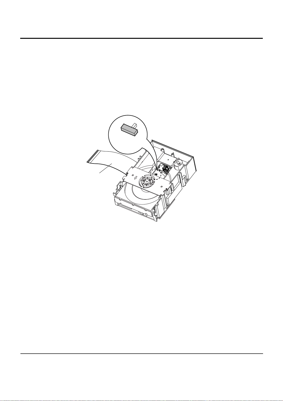
1-5-1 Disassembly
1) Remove the power cable.
2) Switch LD SW3 on deck PCB to ‘S’ before removing the FPC
( inserted into Main PCB CN1. See Fig 1-4.)
3) Disassemble the deck.
4) Disassemble the deck PCB.
5) Replace the Pick-up.
1-5-2 Assembly
1) Replace the Pick-up.
2) Assemble the deck PCB.
3) Reassemble the deck.
4) Switch LD SW3 on deck PCB to ‘O’ and insert
FPC into Main PCB CN1 (See Fig 1-4).
O
S
LD
SW3
FPC
1-5 Pick-up disassembly and ressembly
Note : If the assembly and disassembly are not done in correct sequence, the Pick-up may be damaged.
Fig. 1-4
Samsung Electronics 2-1
2. Reference Information
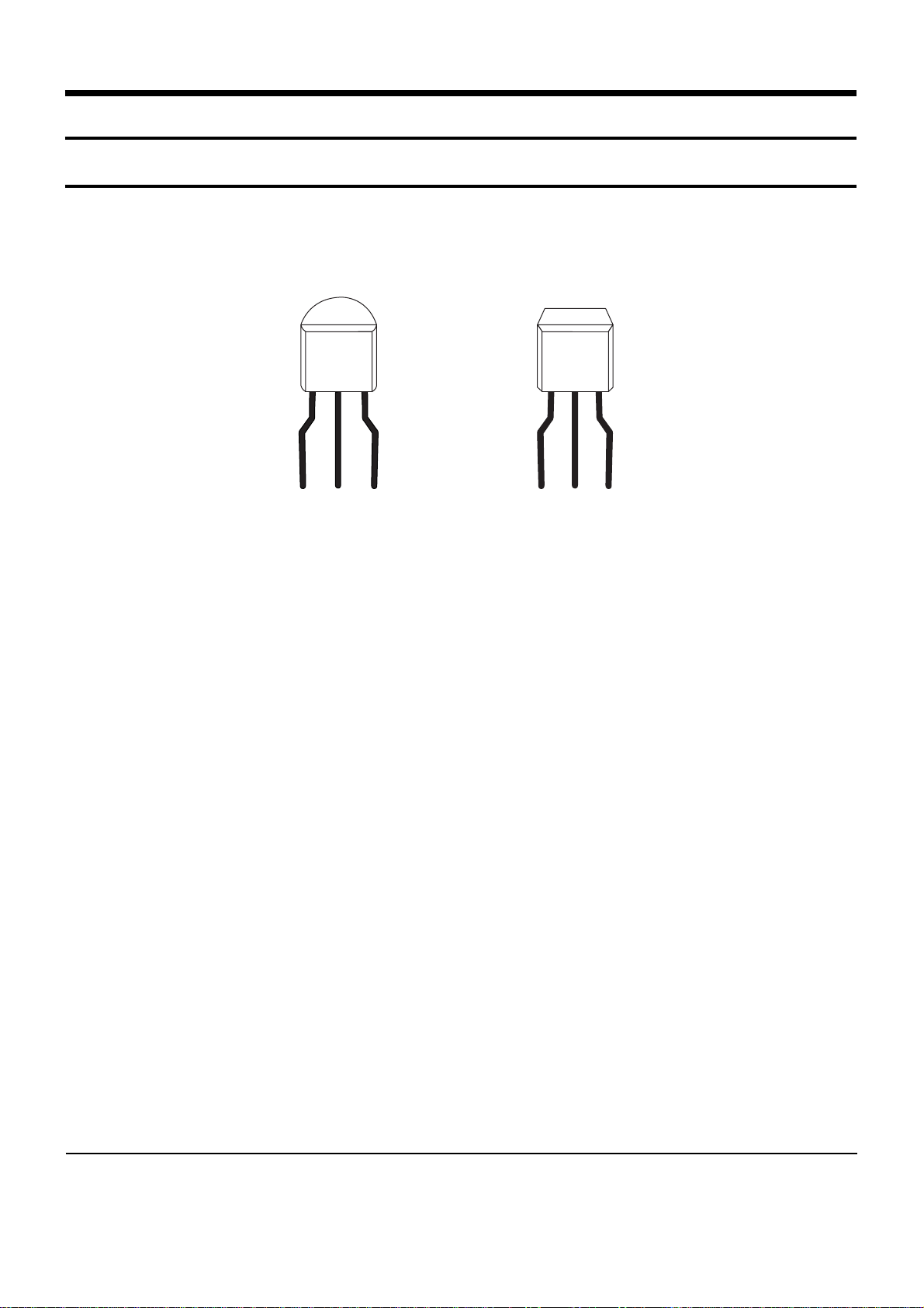
2-1 Semiconductor Base Diagram
Fig. 2-1
RQ1
SS9012
S9012
G-634
E B C
D G S
K184
Y 6A
SQ1
K184
2-2 Samsung Electronics
2-2 Chip Replacement
1) Do not touch the part body directly with the soldering iron. ICs, especially TSOP, are easily damaged by heat.
2) Use care regarding soldering iron tip and avoid
repidly heating parts. Some parts can be damaged
by sudden heating. Preheat the part at about
100°… for several minutes before installing it.
3) Use soldering tip temperature of about 240°… or
larger parts, use a slightly higher temperature
(about 280°…).
4) The thin(0.3mm)solder for miniature parts does
not contain adequate flux. Supplementary flux is
thus needed in most cases.
5) Use care not to damage the circuit pattern, especially when removing.
6) Because of the many pins, cleanliness of the pattern is extremely important after removing the IC.
7) Use care to avoid solder bridges. Remove any that
occurs.
8) Position the part carefully. They will also affect the
soldering operation. Be very precise in positioning
the IC. Soldering opposite pins first holds the IC in
place and makes soldering the other pins easier.
9) Do not reuse removed parts.
10) Check for solder joints, especially miniature parts
with small lead.
11) A defective trimming resistor cannot be adjusted
externally. Replace with an ordjnary variable resistor.
12) It is important to inspect the work with a magnifier.
Check after installing (cold solder joints, etc.).
2-2-1 Precaution for the chip Replacement
The tools for the chip replacement are as follows:
1) Thin tip type soldering iron
2) Small flat-blade tip-type soldering iron
3) Special desoldering tip iron
4) Airblower unit
5) Flat Package Pick-up
6) Flux can be cleaned by water
7) 0.3mm thin solder can be cleaned by water
8) Desoldering wire
9) Tweezers
2-2-2 Tools for the Chip Replacement
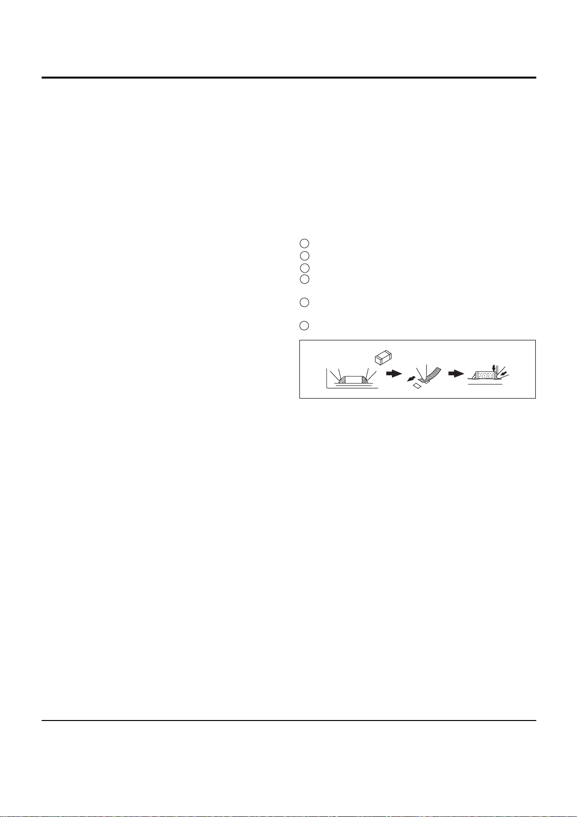
2-2-3 Chip Resistors and Chip Capacitors
-- Kind of the Part
The kind of chip resistors and chip capacitors as follows:d
1) Think Film Chip Resistors
2) Carbon Film Chip Resistors
3) Metal Film Chip Resistors
4) Chip Ceramic Capacitors
5) Chip Trimming Resistors
-- Removing the Part
1) Using two soldering irons:
Use thin tip soldering irons.
Use soldering tip temperature of about 280°….
Simultaneously heat both ends of the part.
While heating, grasp the part with the tips of the
soldering irons and remove it.
Use desoldering wire to completely remove the old
solder from the part location of the board.
A clean pattern for installing the new part is very
important.
Fig 2-2
-- Installing the Part
1) Use desoldering wire to remove the previous solder.
2) Clean the location.
3) Apply flux.
4) Position the IC and solder two pins at opposite sides.
5) Use a sharp tipped soldering iron and carefully
solder each Pin.(After gaining experience, a thicker
tip can be used for better work efficiency.)
6) Remove any solder bridges with desoldering wire.
7) Inspect the work with a magnifier.
1
2
3
4
5
6
Precautions
Samsung Electronics 2-3
-- Kind of the Part
The kind of the part is as follows:
1) Chip VRs.
2) Chip Trimmer Capacitors
3) Diode
4) Transistors
-- Removing the Part
1) Using two soldering irons:
Use small flat-blade tips.
Heat the leads of the part simultaneously.
When the solder melts, grasp and remove the part
with the soldering iron tips.
Remove the old solder with desoldering wire.
2-2-4 Diodes and Tr.
-- The kind of the Chip ICs
The kind of the chip ICs are as follows:
1) SOP(Small Outline Package)IC
2) SSOP(Shrink Small Outline Package)IC
3) VSOP(Very Small Outline Package)IC
4) QFP(Quad Flat Package)IC
5) VQFP(Very Quad Flat Package)IC
6) PLCC(Plastic Leaded Chip Carrier)IC
7) TSOP(Thin Small Outline Package)IC
2-2-5 Chip ICs
-- Removing the Part
1) Using special desoldering iron:
Selet the tip according to the size and shape of the IC.
“Tin” the tip with a small amount of the IC leads.
Set the tip squarely over the IC leads.
When the solder melts, carefully twist the iron.
Raise and remove the IC.
2) Using shaped airblower unit:
Select the correct nozzle.
Select the temperature and airblow(suggested:
temperature:7, airblow:4)
Engage the IC removing tool.
Use the airblow to preheat the IC for about 5
seconds, then heat with the nozzle until the IC
remover lifts the part from the board.
IC
Fig 2-4
-- Installing the Part
1) Use desoldering wire to remove the previous solder.
2) Clean the location.
3) Apply flux.
4) Position the IC and solder two pins at opposite sides.
5) Use a sharp tipped soldering iron and carefully sol
der each Pin.(After gaining experience, a thicker tip
can be used for better work efficiency.)
6) Remove any solder bridges with desoldering wire.
7) Inspect the work with a magnifier.
Fig 2-3
-- Installing the Part
1) Clean the area where the new part is to be mounted.
2) Apply flux.
3) Set part correctly into position, prevent it from shifting.
4) Use sharp soldering iron tip. Bring close to the
part contact without actually touching it. Melt thin
solder between the tip and part si that it flows into
the part contact.
1
234
123
45123
4

Precautions
2-4 Samsung Electronics
MEMO
6-1Samsung Electronics
6-1 DVD DATA PROCESSOR
TC90A19F
DIC1
80 79 78 77 76 75 74 73 72 71 70 69 68 67 66 65 64 63 62 61 60 59 58 57 56 55 54 53 52 51
1 2 3 4 5 6 7 8 9 10 11 12 13 14 15 16 17 18 19 20 21 22 23 24 25 26 27 28 29 30
81828384858687888990919293949596979899
100
81828384858687888990919293949596979899
100
R
VSS
RVR
I
DVR
D
M
O
R
A
S
N
C
A
S
N
M
O
E
N
M
W
E
N
D
VSS
DVD
D
3
M
A
9
M
A
8
M
A
7
M
A
6
M
A
5
M
A
4
M
A
3
M
A
2
M
A
1
M
A
0
D
VSS
DVD
D
5
M
D
7
M
D
6
M
D
5
M
D
4
M
D
3
M
D
2
M
D
1
M
D
0
Memory I/F
De-Scrambler ECC 8/16 DEM Sync Det.
Control
Circuit
Frame Sync
Sector Sync
Frame Number
Correction
PWM
CLV
Contol
RF Signal
Process
PLL
(SVCK)
(PFCK)
HOST INTERFACE
(ECC)
STATUS OUT
UNIVERSAL PWM
(DPCK) (SVCK)
E
D
3
E
D
2
E
D
1
E
D
0
P
L
C
K
H
A
I
H
A
0
HIN
T
DVD
D
5
D
VSS
H
D
7
H
D
6
H
D
5
H
D
4
H
D
3
H
D
2
H
D
1
H
D
0
H
CEN
HDR
D
H
D
W
T
N
C
DVD
D
3
D
VSS
S
VCK
0
DVC
K
1
DVD
D
3
DPC
K
1
D
VSS
D
P
W
M
RFIN
RVDD
RVR2
AVDD
PVR
VRC
AVR
AVSS
SCLO
VCOF
LPFO
LPFN
RLLD
PDOP
PDON
TEST
ED7
ED6
ED5
ED4
SD7
SD6
SD5
SD4
DVSS
DVDD3
SD3
SD2
SD1
SD0
SERR
SBGN
SENB
SDCK
DVSS
SREQ
RSTN
DVDD3
STDA
STCK
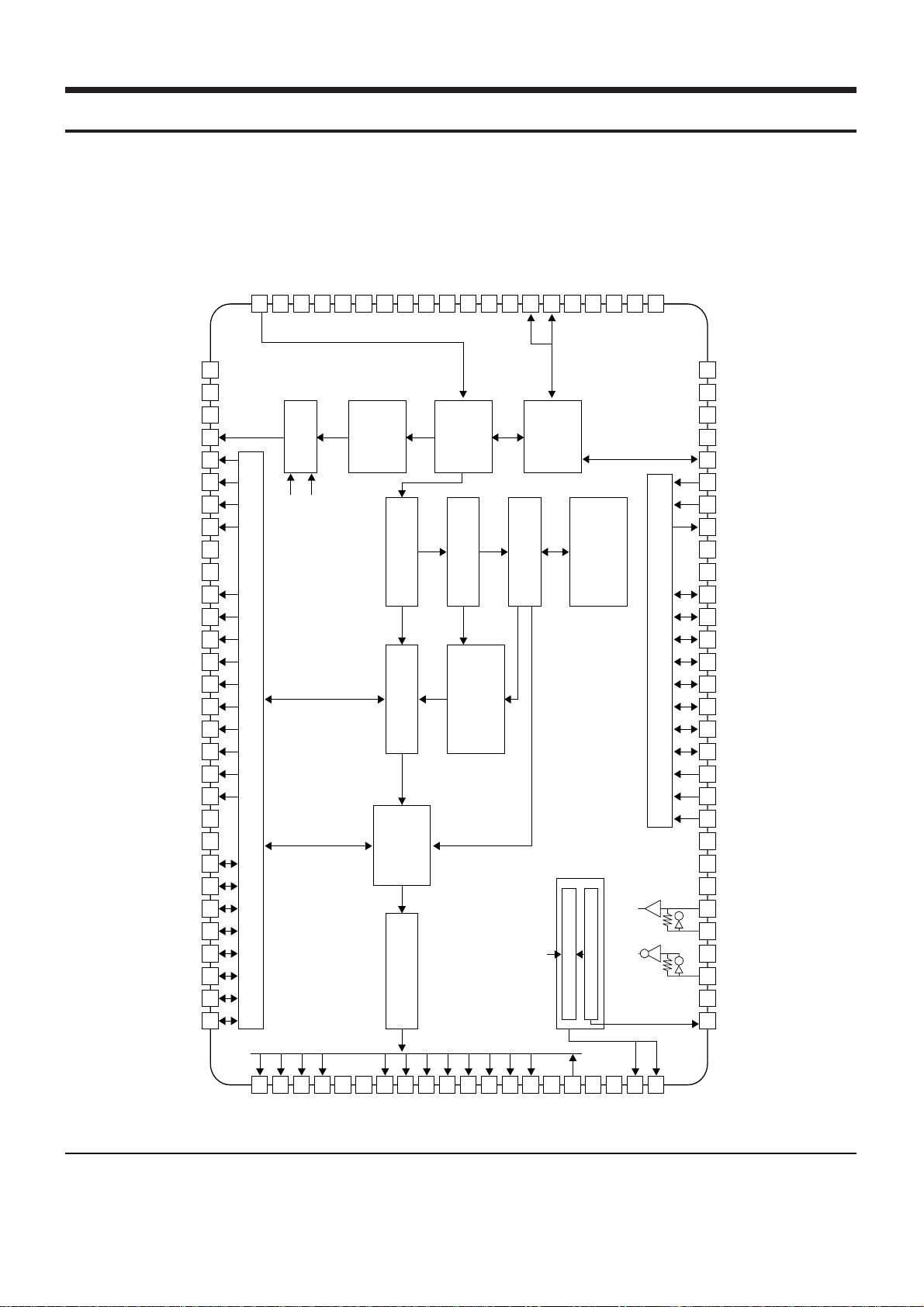
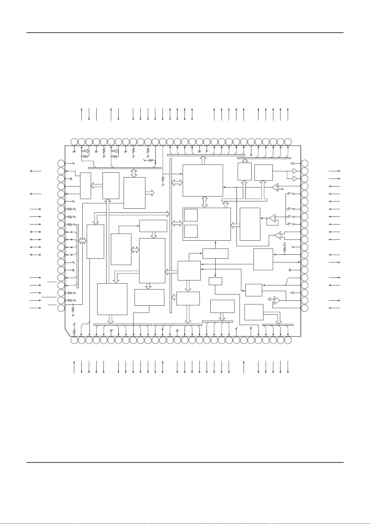
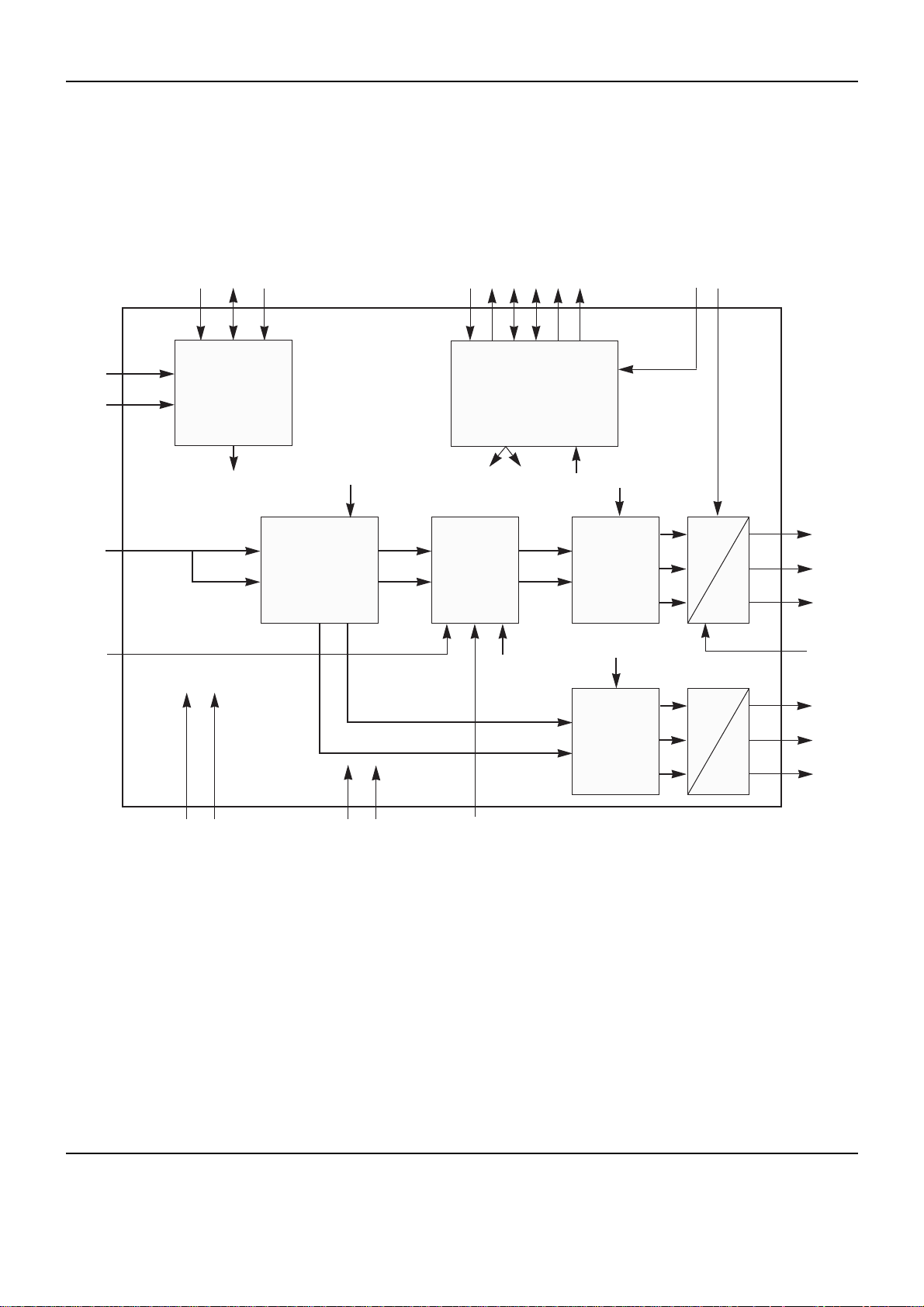
6. IC Descriptions
BLOCK DIAGRAM
IC Descriptions
6-2 Samsung Electronics
PIN ASSIGNMENT
Extension data bus I/O
UPWM
DV
SS1
DPCKI
DVDD1
SVCKI
SVCKO
DV
SS1
DV
DD1
WAIT
HDWT
HDRD
HCEN
HD0
HD1
HD2
HD3
HD4
HD5
HD6
HD7
DV
SS2
DV
DD2
HINT
HA0
HA1
PLCK
ED0
ED1
ED2
ED3
ED4
ED5
ED6
1
2
3
4
5
6
7
8
9
10
11
12
13
14
15
16
17
18
19
20
21
22
23
24
25
26
27
28
29
30
31
32
33
NAME FUNCTION
Wide use PWM output
Digital ground
Signal process reference clock input
(27 to 34MHz)
Digital power supply (3.3V)
Servo reference clock input
(oscillation circuit input)
Servo reference clock output
(oscillation circuit input)
Digital ground
Digital power supply (3.3V)
Waiting
MPU WRITE signal input
MPU READ signal input
MPU chip selection
MPU data bus I/O
MPU data bus I/O
MPU data bus I/O
MPU data bus I/O
MPU data bus I/O
MPU data bus I/O
MPU data bus I/O
MPU data bus I/O
Digital ground
Digital power supply
MPU interruption signal output
(interruption:L)
MPU address bus input
MPU address bus input
VCO oscillation clock I/O
Extension data bus I/O
Extension data bus I/O
Extension data bus I/O
Extension data bus I/O
Extension data bus I/O
Extension data bus I/O
PIN
NAME FUNCTION
PIN
External RAM address bus output
ED7
TEST
PDON
PDOP
TMAX
LPFN
LPFO
VCOF
SLCO
AV
SS
AVR
VRC
PVR
AVDD
RVR2
RV
DD
RFIN
RV
SS
RVR1
DVR
DMO
RASN
CASN
MOEN
MWEN
DV
SS1
DV
DD1
MA9
MA8
MA7
MA6
MA5
34
35
36
37
38
39
40
41
42
43
44
45
46
47
48
49
50
51
52
53
54
55
56
57
58
59
60
61
62
63
64
65
Extension data bus I/O
Test mode input
Phase error signal output(- polarity)
Phase error signal output(+polarity)
RLL detecting result output
Inverting input for PLL loop filter amplifier
Output for PLL loop filter amplifier
VCO filter output
DAC output for making data slice level
Analog ground
Non PLL system analog reference voltage
(1.65V)
Resistor dividing point electrical potential
output(for analog reference electrical potential
generation)
PLL system analog reference voltage
output(1.65V)
Analog power supply (3.3V)
Second reference voltage(for connecting
capacitor)
For power supply
RF signal input
For ground
First reference voltage
(for connecting capacitor)
DMO reference voltage input (2.1V)
Disc equalizer output
(3 value PWM +Hiz) for DVD
External RAM row address selection (negative
logic)
External RAM column address selection
(negative logic)
External RAM output acknowledgement signal
output
External RAM READ/WRITE selection
Digital ground
Digital power supply
External RAM address bus output
External RAM address bus output
External RAM address bus output
External RAM address bus output
IC Descriptions
6-3Samsung Electronics
PIN ASSIGNMENT
MA4
MA3
MA2
MA1
MA0
DV
SS2
DV
DD2
MD7
MD6
MD5
MD4
MD3
MD2
MD1
MD0
SD7
SD6
SD5
SD4
DV
SS1
DV
DD1
SD3
SD2
SD1
SD0
66
67
68
69
70
71
72
73
74
75
76
77
78
79
80
81
82
83
84
85
86
87
88
89
90
External RAM address bus output
External RAM address bus output
External RAM address bus output
External RAM address bus output
External RAM address bus output
Digital ground
Digital power supply
External RAM data bus I/O
External RAM data bus I/O
External RAM data bus I/O
External RAM data bus I/O
External RAM data bus I/O
External RAM data bus I/O
External RAM data bus I/O
External RAM data bus I/O
MPEG data output
MPEG data output
MPEG data output
MPEG data output
Digital ground
Digital power supply
MPEG data output
MPEG data output
MPEG data output
MPEG data output
SERR
SBGN
SENB
SDCK
DV
SS1
SREQ
RSTN
DV
DD1
STDA
STCK
Digital power supply
MPEG data reliability flag output
(data error:L)
MPEG output secter synchronous signal output
(secter top:L)
MPEG data effective flag output (effective:L)
MPEG data transfer clock output
Digital ground
MPEG data request flag input(request:L)
Hard reset input (reset:L)
Operation monitor data output
(Output is carried out in synchronization
with the falling edge of SDCK)
Operation monitor synchronous signal
output (data top bit:L)
91
92
93
94
95
96
97
98
99
100
NAME FUNCTION
PIN
NAME FUNCTION
PIN
IC Descriptions
6-4 Samsung Electronics
6-2 RF IC
TA1236F
RIC1
48 47 46 45 44 43 42 41 40 39 38 37 36 35 34 33
32
31
30
29
28
27
26
25
24
23
22
21
20
19
18
17
1 2 3 4 5 6 7 8 9 10 11 12 13 14 15 16
49
50
51
52
53
54
55
56
57
58
59
60
61
62
63
64
LPF
LPF
LPF
SEL
Vref
Focus
Error
Detector
LD-APC
LD-Po Sel.
ATT
CD-EQ
DVD-EQ
VCA
DVD-EQ
SEL
Peak &
Bottom
Detector
SEL
Ripple
Detector
VREF & 2VR
GEN.
TIME-CON.
LPF
Fullwave
RECT.
GND3
RFR FIL
RFRP
OUT
RFcen
FWR FIL
FE
OUT
FE
IN
DVDGD
NC
PRE FIL
NC
TE
OUT
V
ref
V
ref
FIL
2V
ref
2V
ref
FIL
GND2
MCK
ADJ. FIL
Vcc2
RPD etP
DetSR
RPDetB
GND1
DPD
TE
NC
3B
OUT
3B
IN
3BTE
SB
OUT
SB
IN
TE BAL
S/D sel
F
IN
E
IN
V
refIN
D
IN
C
IN
B
IN
A
IN
Vcc1
RFN
IN
RFP
IN
LDP
sel
OUT
LDC
Vcc3
MD
IN
RF
Gain
DVD
sel
EQ
OUTEQINSQsel
DVD EQ
CDEQ
DVD
Time
CD
Time
RF CD
OUT
DPD/3B sel
Vcc4
RF
cen
P
RF
cen
B
RF DVD
OUT
RP
sel
BLOCK DIAGRAM
IC Descriptions
6-5Samsung Electronics
RF system ground
TEB
SBI
SBAD
3BTE
3BIN
3BO
N.C.
TE1B
GNDSV
RFB
DETR
RFP
V
CCD
ADJF
MCK
GNDD2
2CVR
2VR
CVR
V
REF
TEO
N.C.
RFDEQ
N.C.
EQGD
FEI
FEO
3TF
RFZC
RFRP
RPF
GNDRF
1
2
3
4
5
6
7
8
9
10
11
12
13
14
15
16
17
18
19
20
21
22
23
24
25
26
27
28
29
30
31
32
Control input to change sub beam
subtraction ratio at-3beam system tracking
error(TE)generation
Inverting input for sub-beam summing
amplifier
Sub-beam summing amplifier output
3 beam TE signal intermediate output
Amplifier inverting input for 3 beam TE
level adjustment
Amplifier output for 3 beam TE level adjustment
No connection
DPD system TE signal input
Servo system ground
RF ripple datector
RF ripple datector
RF ripple datector
Power supply
Filter external capacitor for DVD-EQ time
constant compensation
Clock input for DVD-EQ time constant
compensation
Ground
Reference voltage smoothing external capacitor
Reference voltage twice output
Reference voltage smoothing external capacitor
Reference voltage output
TE output after switching DPD/3B
No connection
Pre filter output for RF
No connection
Group delay characteristic control input for
DVD-EQ
Inverting input for focus error(FE) signal output
amplifier
FE output
Filter external capacitor to DVD-WV
detecting signal
Amplitude center voltage output of RF ripple
signal
RF ripple signal output
Filter external capacitor for RFRP signal
Control input when selecting DVD-WV
detecting signal for RFRP
RPS
SFSD
RFZB
RFZP
V
CC3
1B3B
RFCD
CD
TIME
CDF
FREQ
HSB
EQI
EQO
CD/SD
RFG
V
CCRF
MDI
LDC
LDO
LDP
RFP
RFN
V
CC5V
AI
BI
CI
DI
V
IRF
TNI
TPI
DBL
33
34
35
36
37
38
39
40
41
42
43
44
45
46
47
48
49
50
51
52
53
54
55
56
57
58
59
60
61
62
63
64
EQ output for DVD
RFRP center level detection
RFRP center level detection
Power supply for reference voltage
Control input to select DPD or 3B for TE
Signal
EQ output for CD
Frequency adjustment input for CD-EQ
curve
Frequency adjustment input for DVD-EQ
curve
Peak gain adjustment input for CD-EQ curve
DVD-EQ curve peak gain adjustment Input
Normal/four times linear speed selecting input
for CD-EQ
DVD/CD-EQ input
VCA passing Output for RFN and RFP
Selection control input for DVD-CD
Control input for RF signal VCA
RF system power supply
Monitoring input for laser diode APC
ON/OFF control input for LD
External current driver control output
for LD
Selection input for APC control polarity
RF signal non-inverting input from PU
RF signal inverting input from PU
Servo system power supply
Main beam four divisions detector A input for
making focus error (FE)
Main beam four divisions detector B input for
making FE
Main beam four divisions detector C input for
making FE
Main beam four divisions detector D input for
making FE
2.1V reference voltage input
Sub-beam E input
Sub-beam F input
Single/double layer system
selection input
NAME FUNCTION
PIN
NAME FUNCTION
PIN
PIN ASSIGNMENT
IC Descriptions
6-6 Samsung Electronics
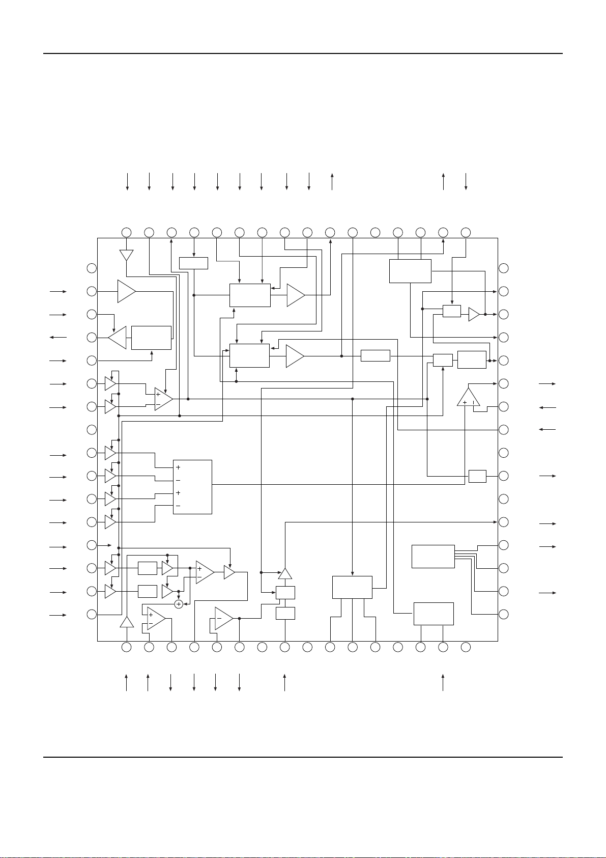
6-3 SERVO & CD DATA PROCESSOR
TC9420F
SIC7
1234567
8
9
101112131415161718192021222324252627282930
8079787776757473727170696867666564636261605958575655545352
51
50
49
48
47
46
45
44
43
42
41
40
39
38
37
36
35
34
33
32
31
VREE
TRO
FOO
TEZI
TEI
TSIN
SBAD
FEI
RFRP
RFZI
RFCT
AVDD
RFI
SLCO
AVSS
VCOF
VCOREF
PVREF
LPFO
LPFN
81
82
83
84
85
86
87
88
89
90
91
92
93
94
95
96
97
98
99
100
DVDD
RO
DVSS
DVR
LO
DVDD
TEST1
TEST2
TEST3
BUS0
BUS1
BUS2
BUS3
VDD
VSS
BUCK
CCE
TEST4
TSMOD
RST
XVDDXOXI
XVSS
VDD
PXO
PXI
VSS
TESIO1
TESIN
DACT
CKSE
DMOUT
IO3
IO2
IO1
IO0
VSS
VDD
FLGD
FLGC
FLGB
FLGA
SEL
2VREF
DMO
FVO
FMO
TEBC
RFGC
TEST0
HSO
UHSO
EMPH
LRCK
VSS
BCK
AOUT
DOUT
MBOV
IPF
SBOK
CLCK
VDD
VSS
DATA
SFSY
SBSY
SPCK
SPDA
COFS
MONIT
VDD
TESIO0
P2VREF
SPDO
PDOS
PDO
TMAXS
TMAX
LPF
1bit
DAC
clock
Generatev
micom
interface
Audio
out
Digital out
status
PLL
TMAX
VCO
PWM
Data
slia
A/D
D/A
PWM
Servo
control
ROM
RAM
16k RAM
Address
Circuit
CLV SERVO
EFM
Digital
EQ
Demod.
Compen-
sating
Circuit
BLOCK DIAGRAM
IC Descriptions
6-7Samsung Electronics
Amplifier (for low pass filter)output
TEST0
/HSO
/UHSO
EMPH
LRCK
V
SS
BCK
AOUT
DOUT
MBOV
IPF
SBOK
CLCK
V
DD
V
SS
DATA
SFSY
SBSY
SPCK
SPDA
COFS
MONIT
VDD
TESIO0
P2V
REF
SPDO
POOS
PDO
TMAXS
TMAX
LPFN
LPFO
1
2
3
4
5
6
7
8
9
10
11
12
13
14
15
16
17
18
19
20
21
22
23
24
25
26
27
28
29
30
31
32
For test mode
Playback speed mode flag ouput
Playback speed mode flag output
Emphasis flag output of sub-code Q
data(H:emphasis ON,L:emphasis OFF)
Channel clock(44.1kHz)output
Digital ground
Bit clock(1.4122MHz) output
Audio data output
Digital Out output
Buffer memory over signal output
Compensation flag output
CRCC judging result output of sub-code Q
data(result OK:H)
Clock I/O
(for sub-code P to W data reading)
Digital + power supply
Digital ground
Sub-code P to W data output
Playback system frame synchronous signal
output or Servo system internal register data
Read clock output
Sub-code block synchronous output or
Servo system internal register data latch pulse
output
Processor status signal Read clock
(176.4kHz)output
Processor status signal output
Correction system frame clock(7.35khz) output
LSI internal signal monitor output
Digital + power supply
Test I/O
2VREF terminal for PLL system
VCO center frequency shift output
Phase difference signal output between
EFM signal and PLCK signal
(at 8 times speed operation)
Phase difference signal output between EFM
signal and PLCK signal
TMAX detection result output
TMAX detection result output
Amplifier (for low pass filter)
inverting input
Wide use I/O port
PV
REF
VCO
REF
VCOF
AV
SS
SLCO
RFI
AV
DD
RFCT
RFZI
RFRP
FEI
SBAD
TSIN
TEI
TEZI
FOO
TRO
V
REF
RFGC
TEBC
FMO
FVO
DMO
2V
REF
SEL
FLGA
FLGB
FLGC
FLGD
V
DD
V
SS
IO0(FMOP)
I
O1(FMON
)
33
34
35
36
37
38
39
40
41
42
43
44
45
46
47
48
49
50
51
52
53
54
55
56
57
58
59
60
61
62
63
64
65
VREF terminal for PLL system
VCO center frequency reference level
Filter terminal for VCO
Analog system ground
Data slice level making DAC output
RF signal input
Analog system power supply
RFRT signal center level input
RFRT zero cross input
RF ripply signal input
Focus error signal input
Sub-beam addition signal input
Input terminal
(in case of tracking of mode)
Tracking error input
Input for tracking error, zero cross
Focus equalizer output
Tracking equalizer output
Analog reference power supply
RF amplitude adjustment control signal output
Tracking balance control signal output
Feed equalizer output
Speed error signal of feed search EQ output
Disc equalizer output
Analog reference power sypply (2x V
REF
)
APC circuit ON/OFF signal output
External floag output
(for monitoring internal signal)
External floag output
(for monitoring internal signal)
External floag output
(for monitoring internal signal)
External floag output
(for monitoring internal signal)
Digital + power supply
Digital ground
Wide use I/O port
NAME FUNCTION
PIN
NAME FUNCTION
PIN
PIN ASSIGNMENT
IC Descriptions
6-8 Samsung Electronics
IO2(DMOP)
IO2(DMON)
/DMOUT
/CKSE
/DACT
TESIN
TESIO1
V
SS
PXI
PXO
V
DD
XVSS
XI
XO
XV
DD
DVDO
RO
DV
SS
DVR
LO
DV
DD
TEST1
TEST2
TEST3
BUS0
66
67
68
69
70
71
72
73
74
75
76
77
78
79
80
81
82
83
84
85
86
87
88
89
90
Wide use I/O port
Wide use I/O port
Mode setting to output binary PWM signals of field
equalizer from IO0 and IO1 terminals and of disc
equalizer from IO2 and IO3 terminals
X¡fltal selection
DAC test mode
Test input (external VCO clock input)
Test I/O
Digital ground
DPS system clock oscillation circuit input
DPS system clock oscillation circuit output
Digital + power supply
Ground for system clock oscillation circuit
System clock oscillation circuit input
System clock oscillation circuit output
+ power supply for system clock oscillation
circuit
D/A converting section power supply
R channel data forward rotation output
D/A converting section ground
D/A converting section reference voltage
L channel data forward rotation output
D/A converting section power supply
Test mode terminal
Test mode terminal
Test mode terminal
Data I/O (for microcomputer interface)
BUS1
BUS2
BUS3
V
DD
VSS
BUCK
/CCE
TEST4
/TSMOD
/RST
91
92
93
94
95
96
97
98
99
100
Chip enable signal input for microcomputer
interface
Data I/O (for microcomputer interface)
Data I/O (for microcomputer interface)
Data I/O (for microcomputer interface)
Digital + power supply
Digital ground
Clock input for microcomputer interface
Test mode terminal
Local test mode selection
Reset signal input
NAME FUNCTION
PIN
NAME FUNCTION
PIN
PIN ASSIGNMENT
IC Descriptions
6-9Samsung Electronics
6-4 AUDIO/VIDEO DECODER
ZiVA D6-L
BIC1
Memory
Controller
OSD
Decoder
Video
Mixer
Video
Interface
Audio
Interface
Sync
Generator
Subpicture
Decoder
MPEG
Video
Decoder
Dolby Digital
Audio
Decoder
MPEG
Audio
Decoder
Host
Interface
Control Logic
Program
Stream
Decoder
DRAM/
ROM
Interface
Host
Interface
DVD/CD
Interface
ZZiiVVAA DD eecc oodd eerr
BLOCK DIAGRAM
Digital Audio
and
IEC-958
Interface
IC Descriptions
6-10 Samsung Electronics
LOGIC DIAGRAM
HADDR[2:0]
CS
R/W (M Mode)/WR (I Mode)
RD (I Mode)
HDATA[7:0]
WAIT
INT
Host
Interface
Signals
Video
Interface
Signals
DVD/CD
Interface
Signals
Audio
Interface
Signals
DRAM/ROM
Interface
Signals
Global
Interface
Signals
DA-DATA[2:0]
*
DA-LRCK
DA-BCK
DA-XCK
IEC958
MADDR[8:0]/MROMA[8:0]
MADDRH4
MADDRH1
MDATA[31:0]
MDATA[47:32]/MROMDATA[15:0]
MDATA[60:48]/MROMA[21:9]
MDATA[63:61]
MRAS1
MRAS0
MCAS[1:0]
MWE
MCE
SYSCLK
VDD
VSS
A_VSS
A_VDD
VDD5MAX
RESET
VDATA[7:0]
HSYNC
VSYNC
VCK
DVD-DATA[0]/CD-DATA
DVD-DATA[1]/CD-LRCK
DVD-DATA[2]/CD-BCK
DVD-DATA[3]/CD-C2PO
DVD-DATA[4]
DVD-DATA[5]
DVD-DATA[6]
DVD-DATA[7]
REQUEST
CSTROBE
ERROR
DACK
IC Descriptions
6-11Samsung Electronics
6-5 MAIN MICOM
TMP93CS41
MIC1
PAO~PA6
PA7(SCOUT)
P50 to P57
(ANO to AN7)
AVCC
AVSS
VREFH
VREFL
(TXD0)P90
(RXD0)P91
(SCLK0/CTS0)P92
(TXD1)P93
(RXD1)P94
(SCLK1)P95
(PG 00)P60
(PG 01)P61
(PG 02)P62
(PG 03)P63
(PG 10)P64
(PG 11)P65
(PG 12)P66
(PG 13)P67
(T10)P70
(T01)P71
(T02)P72
(T03)P73
(INT4/T14)P80
(INT5/T15)P81
(T04)P82
(T05)P83
(INT6/T16)P84
(INT7/T17)P85
(T06)P86
(INTO)P87
VCC[3]
VSS[3]
X1
X2
CLK
XT1
XT2
AM8/16
EA
RESET
ALE
TEST2,1
NMI
WDTOUT
P00 to P07
(AD0 to AC7)
P10 to P17
(AD8 to AD15/A8 toA15
P20 to P27
(A0 to A7/A16 to A23)
P30(RD)
P31(WR)
P32(HWR)
P33(WAIT)
P34(BUSRQ)
P35(BUSAK)
P36(R/W)
P37(RAS)
P40(CS0/CAS0)
P41(CS1/CAS1)
P42(CX2/CAS2)
cPORT A
High
Frequency
OSC
Low
Frequency
OSC
INTERRUPT
CONTROLLER
WATCH-DOG
TIMER
PORT 0
PORT 2
PORT 3
CS/WAIT
CONTROLLER
(3-BLOCK)
PORT 1
10-BIT 8CH
A/D
CONVERTER
SERIAL I/O
(CH,0)
SERIAL I/O
(CH,1)
PATTERN
GENERATOR
(CH,0)
PATTERN
GENERATOR
(CH,1)
16BIT TIMER
(TIMER 4)
16BIT TIMER
(TIMER 5)
8BIT TIMER
(TIMER 0)
8BIT TIMER
(TIMER 1)
8BIT PWM
(TIMER 2)
8BIT PWM
(TIMER 3)
900L-CPU
2KB RAM
XWA
XBC
ADE
XHL
XIX
XIY
XIZ
XSP
W
B
D
H
IX
IY
IZ
SP
A
C
E
L
32bit
FSR
P C
BLOCK DIAGRAM
IC Descriptions
6-12 Samsung Electronics
/CCE
BUCK
TEST1
TEST2
BUS0
BUS1
BUS2
BUS3
RPSEL
DFS
ALE
VCC
AD0
AD1
AD2
AD3
AD4
AD5
AD6
AD7
AD8
AD9
AD10
AD11
AD12
AD13
AD14
AD15
P96
P97
Test1
Test2
PA0
PA1
PA2
PA3
PA4
PA5
PA6
PA7
ALE
VCC
P00
P01
P02
P03
P04
P05
P06
P07
P10
P11
P12
P13
P14
P15
P16
P17
31
32
33
34
35
36
37
38
39
40
41
42
43
44
45
46
47
48
49
50
51
52
53
54
55
56
57
58
59
60
O
O
O
I
I/O
I/O
I/O
I/O
O
O
O
O
O
O
I/O
I/O
I/O
I/O
I/O
I/O
I/O
I/O
I/O
I/O
I/O
I/O
I/O
I/O
I/O
I/O
Digital Servo Chip Enable
Digital Servo I/F Clock
Digital Servo I/F Data 0
Digital Servo I/F Data 1
Digital Servo I/F Data 2
Digital Servo I/F Data 3
Ripple Detect Output S/W
“H”=96KHz
Address Chip Enable
+5V
Address/Data Bus0
Address/Data Bus1
Address/Data Bus2
Address/Data Bus3
Address/Data Bus4
Address/Data Bus5
Address/Data Bus6
Address/Data Bus7
Address/Data Bus8
Address/Data Bus9
Address/Data Bus10
Address/Data Bus11
Address/Data Bus12
Address/Data Bus13
Address/Data Bus14
Address/Data Bus15
VREFL
AVSS
AVCC
SRQ
RRQ
LDON
SLEDOUT
SLEDIN
SLEDFG
DSPLT
DIF2
ML1
SBSY
DVDINT
MRST
DPINT
TXD
RXD
SCLK
MD
ML2
MC
AM8/16
CLK
V
CC
Vss
X1
X2
EA
RESET
NMI
P70
P71
P72
P73
P80
P81
P82
P83
P84
P85
P86
P87
P90
P91
P92
P93
P94
P95
AM8/16
CLK
V
CC
VSS
X1
X2
EA
Reset
1
2
3
4
5
6
7
8
9
10
11
12
13
14
15
16
17
18
19
20
21
22
23
24
25
26
27
28
29
30
I
I
I
I
O
O
O
O
I
O
O
O
I
O
O
I
O
I
I
O
O
O
I
O
I
I
I
O
I
I
FUNCTION
PIN I/O NAME
Reference Voltage Input to A/DC(¡ L¡–)
GND pin for A/D Converter(0V)
Power supply pin for A/D Converter
Fromt Micom - -> Main Micom Request
Fromt Micom <- - Main Micom Request
Laser On (“H”=on)
Forward Slide Move
Reverse Slide Move
Hall Count Input
Sony DSP Data Latch
AKM4324 Control(“L”=16/20bit, “H”=24bit)
Audio DAC Data Latch 1
SUBQ Block Sync. Signal INT.
A/V Decoder INT.
LSI Reset
Data Processor INT.
Front Micom Trans. Data
Front Micom Receive Data
Front Micom Communication Clock
Audio DAC Trans. Data
Audio DAC Data Latch 2
Audio DAC Trans. Clock
8bit External Data Bus Width(¡ H¡–)
Clock Output(System Clock/2)
Power Supply Pin(+5V)
GND Pin(0V)
20MHz
20MHz
TMP93CS41F:¡–L¡–
Micom Rest Input
FUNCTION
PIN I/O NAME
PIN ASSIGNMENT
IC Descriptions
6-13Samsung Electronics
VSS
VCC
A16
A17
A18
A19
A20
A21
A22
A23
/RD
/WR
ML0/DIF0
WAIT
/BUSRQ
/BUSAK
ED_K
ED_T
/CS0
/CS1
/CS2
DVD_SEL
OPEN
CLOSE
S/D_SEL
SDA
SCL
BASS
SLEDGS
WDTO
V
SS
V
CC
A16
A17
A18
A19
A20
A21
A22
A23
P30
P31
P32
P33
P34
P35
P36
P37
P40
P41
P42
P60
P61
P62
P63
P64
P65
P66
P67
61
62
63
64
65
66
67
68
69
70
71
72
73
74
75
76
77
78
79
80
81
82
83
84
85
86
87
88
89
90
I/O
O
O
O
O
O
O
O
O
O
O
O
I
I
O
O
O
O
O
O
O
O
O
O
O
O
O
O
GND(0V)
+5V
Address Bus 16
Address Bus 17
Address Bus 18
Address Bus 20
Address Bus 21
Address Bus 22
Address Bus 23
Strobe for Reading External Momory
Strobe for Writing Data AD0 to AD7
Audio DAC Data Latch 0
/AKM4324 Control(“L”=16/24bit, “H”=20bit)
Address Bus 19
Request CPU Bus Wait
Bus Request
Bus Acknowledge
EEPROM Trans. Clock(I2S)
EEPROM Trans. Data(I2S)
Chip Select 0
Chip Select 1
Chip Select 2
DVD/CD Mode Control(DVD=”Low”)
Door Open Motor Control
Door Close Motor Control
Single/Dual Disc Select(Single=”Low”)
Video Encoder Trans. Data(l
2
C)
Video Encoder Trans. Clock(l
2
C)
Bass Redirection Control(“L”=SW On, “H”=SW Off)
Sled Gain Select
FUNCTION
PIN I/O NAME
FUNCTION
PIN I/O NAME
VSS
FEI
SPFG
/SECAM
/PAL
/NTSC
OP-SW
CL-SW
VREFH
V
SS
P50
P51
P52
P53
P54
P55
P56
P57
VREFH
91
92
93
94
95
96
97
98
99
100
I
I
I
I
I
I
I
I
I
GND
Focus Error Input
Spindle FG Input
SECAM=”H”
PAL =”H”
NTSC=”H”
Door Open SW
Door Close SW
Reference Voltage Input to A/DC(¡ H¡–)
PIN ASSIGNMENT
IC Descriptions
6-14 Samsung Electronics
6-6 DIGITAL VIDEO ENCODER
SAA7128
VIC1
I'C-
INTERFACE
SYNC/
CLOCK
MP
MP
9..16
44
20
21
I'C-Control
I'C-Control
I'C-Control
I'C-Control
I'C-Control
Clock&Timing
RESN
40
42
41
35
34
7
8
43
37
4
25,28,31,36
SDA
SCL
XTALI
XTAL
RCV1
RCV2
TTXRQ
XCLK
LLC1
VDDA
VDD I2C
SA
MP(7:0)
TTX
FADER
ENCODER
OUTPUT-
INTERFACE
D
A
RGB-
PROCESSOR
D
22,32,33
23
26
29
30
27
Y
C
Y
5,18,38
6,17,39
2
3
VSS
VDD
SP
AP
19
RTC1
CbCr
Y
CbCr
24
R(Cr)
VSSA
G(Y)
B(Cb)
CVBS
(CSYNC)
VBS
(CVBS)
C
(CVBS)
A
BLOCK DIAGRAM
IC Descriptions
6-15Samsung Electronics
NAME
res.
SP
AP
LLC1
V
SS1
VDD1
RCV1
RCV2
MP7
MP6
MP5
MP4
MP3
MP2
MP1
MP0
V
DD2
VSS2
RTCI
VDD
12C
SA
V
SSA1
R(Cr)
C
V
DDA1
G(Y)
VBS
V
DDA2
B(Cb)
CVBS
V
DDA3
VSSA2
VSSA3
XTAL
XTAL1
I/O
I
I
I
I
I
I/O
I/O
I
I
I
I
I
I
I
I
I
I
I
I
I
I
O
O
I
O
O
I
O
O
I
I
I
O
I
PIN
1
2
3
4
5
6
7
8
9
10
11
12
13
14
15
16
17
18
19
20
21
22
23
24
25
26
27
28
29
30
31
32
33
34
35
FUNCTION
reserved pin, do not connect
Test Pin;connected to digital ground for normal operation
Test Pin;connected to digital ground for normal operation
Line-Locked Clock input;this is the 27 MHz master clock
digital supply ground 1
digital supply 1
digital supply voltage 2
digital ground 2
Real Time Control input. If the LLC1 clock is provided by an SAA7111 or SAA7151B,
RTCI should be connected to the RTCO pin of the respective decoder to improve the
signal quality.
Sense input for 12C bus voltage;connect to 12C bus supply
Select 12C address; low selects slave address 88h, high selects slave address 8Ch.
Analog ground 1 for Red (Cr), C(CVBS), Green(Y) outputs
Analog ground 3 for the DAC reference ladder and the oscillator
Crystal oscillator output
Crystal oscillator input; if the oscillator is not used, this pin should be connected to
ground.
Analog output of Red (Cr)signal
Analog output of Chrominance (CVBS) signal
Analog supply voltage 1 for R(Cr), C(CVBS) outputs
Analog output of Green(Y) signal
Analog output of VBS (CVBS) signal
Analog supply voltage 2 for VBS(CVBS), Green(Y) outputs
Analog output of Blue(Cb) signal
Analog output of CVBS(CSYNC) signal
Analog supply voltage 3 for Blue(Cb)and CVBS(CSYNC), outputs
Analog ground 2 for VBS (CVBS), Blue(Cb), CVBS(CSYNC)outputs
Raster Contral 1 for video port. This pin receives/provides a VS/FS/FSEQ signal.
Raster Contral 2 for video port. This pin provides an HS pulse of programmable length
or receives an HS pulse.
Double speed 54 MHzMPEG port. It is an input for ¡
CCIR 656
¡–style multiplexed Cb, Y,
Cr data. Data are sampled on the rising and falling clock edge;data sampled on the
risting edge then are sent to the encoding part of the device, data sampled on the
falling edge are sent to the RGB part of the device.(or vice verse, depending on
programming)
PIN ASSIGNMENT
IC Descriptions
6-16 Samsung Electronics
NAME
V
DDA4
XCLK
V
SS3
VDD3
RESN
SCL
SDA
TTXRQ
TTX
PIN ASSIGNMENT
I/O
I
O
I
I
I
I
I/O
O
I
PIN
36
37
38
39
40
41
42
43
44
FUNCTION
Analog supply voltage 4 for the DAC reference ladder and the oscillator
Clock output of the crystal oscillator
digital supply ground 3
digital supply 3
12C serial clock input
12C serial data input/output
Teletext Request output, indicating when text bits are requested
Teletext bit stream input
Reset input, active LOW. After reset is applied, all digital I/Os are in input mode; PALBlackburst on CVBS, VBS and C;RGB outputs set to lowest voltage.
The 12C-bus receiver waits for the START condition.
IC Descriptions
6-17Samsung Electronics
6-7 DIGITAL-TO-ANALOG CONVERTER
PCM 1720
AIC1(Rev.1), AIC2
1
2
3
4
¡
5
¡
6
¡
7
¡
8
9
10
11
12
13
14
¡
15
¡
16
¡
17
18
19
20
NC
SCKI
TEST
ML
MC
MD
RSTB
ZERO
V
OUT
R
AGHD
V
CC
V
OUT
L
CAP
BCKIN
DIN
LRCIN
NC
NC
V
DD
DGND
NAME
Low-pass
Filter
V
OUT
L
CAP
V
OUT
R
ZERO
Multi-level
Dalta-Sigma
Modulator
BPZ-Cont.
SCKI
256fs/384f
s
Low-pass
Filter
DAC
BLOCK DIAGRAM
PIN ASSIGNMENT
8X Oversampling
Digital Filter
with Function
Controller
Multi-level
Dalta-Sigma
Modulator
Serial
Input
I/F
Mode
Control
I/F
Power Supply
Open Drain
BCKIN
LRCIN
DIN
ML
MC
MD
RSTB
DAC
VCCAGND VDDDGND
PIN
I/O
-
IN
OUT
IN
IN
IN
IN
OUT
OUT
PWR
PWR
OUT
-
IN
IN
IN
-
-
PWR
PWR
FUNCTION
No Connection.
System Clock input: 256fsor 384fs.
Reserved for Factory Use.
Latch Enable for Serial Control Data.
Clock for Serial Control Data.
Data Input for Serial Control.
Reset Input. When this pin is low, the digital filters and modulators are held in reset.
Zero Data Flag. This pin is low when the data is continuously zero for more than
65,535 cycles ro BCKIN.
Right Channel Analog Output.
Analog Ground.
Analog Power Supply (+5V).
Left Channel Analog Output.
Common Pin for Analog Output Amplifiers.
Bit Clock for Clocking in the Audio Data.
Serial Audio Data input.
Left/Right Word Clock. Frequency is equal to fs.
No Connection.
No Connection.
Digital Power supply(+5V). Recommended connection is to the analog power supply.
Digital Ground. Recommended connection is to the digital ground plane.
¡
These pins include internal pull-up resistors.
IC Descriptions
6-18 Samsung Electronics
6-8 DIGITAL-TO-ANALOG CONVERTER WITH PLL
PCM 1723
AIC3
Low-pass
Filter
V
OUTL
CAP
V
OUTR
ZERO
Multi-level
Dalta-Sigma
Modulator
BPZ-Cont.
OSCPLL
SCKO
MCKO XTI XTO
256fs/384f
s
Low-pass
Filter
DAC
BLOCK DIAGRAM
8X Oversampling
Digital Filter
with Function
Controller
Multi-level
Dalta-Sigma
Modulator
Serial
Input
I/F
Mode
Control
I/F
Power Supply
BCKIN
LRCIN
DIN
ML
MC
MD
RSTB
DAC
VCP PGND VCC AGND VDD DGND
PIN ASSIGNMENT
PIN
NAME
I/O
1
2
3
4
5
6
'
7
'
8
'
9
'
10
11
12
13
14
15
16
'Ł
17
'Ł
18
'Ł
19
20
21
22
23
24
XTI
SCKO
V
CP
NC
MCKO
ML
MC
MD
RSTB
ZERO
V
OUT
B
AGND
V
CC
V
OUT
L
CAP
BCKIN
DIN
LRCIN
NC
RES
V
DD
DGND
PGND
XTO
IN
OUT
PWR
N/A
OUT
IN
IN
IN
IN
OUT
OUT
GND
PWR
OUT
IN
IN
IN
N/A
N/A
PWR
GND
GND
Out
FUNCTION
Master Clock Input.
System Clock Out. This output is 256fsor 384fs.
system clock generated by the internal PLL.
PLL Power Supply (+5V).
No Connection.
Buffered clock output of crystal oscillator.
Latch for serial control data.
Clock for serial control data.
Data for serial control.
Reset Input. When this pin is low, the digital filters and modulators are held in reset.
Zero Data Flag. This pin is low when the input data is continuously zero for more than
65,535 cycles ro BCKIN.
Right Channel Analog Output.
Analog Ground.
Analog Power Supply (+5V).
Left Channel Analog Output.
Common Pin for analog output amplifiers.
Bit Cclock for clocking in the audio data.
Serial audio data input.
Left/Right Word Clock. Frequency is equal to fs.
No Connection.
Reserved for factory use, do not connect.
Analog Power Supply (+5V).
Digital Ground.
PLL Ground.
Crystal oscillator output.
Note:(1)Schmitt triger input with intermal pull-up resistors. (2) Schmitt triger input.
 Loading...