Samsung Electronics 2-1
2-1-1 Comparison between linear power supply and SMPS
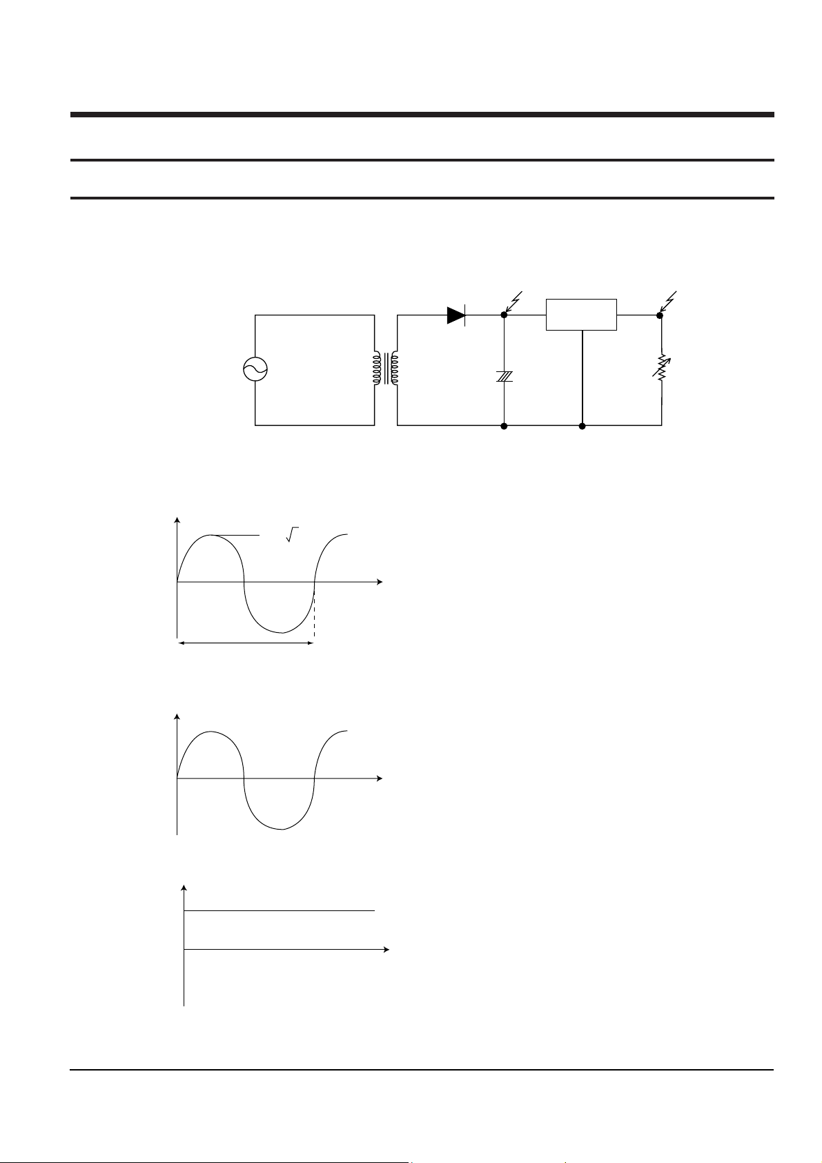
2-1-1(a) LINEAR
Fig. 2-1
Input : Common power to transformer(Vp)
Fig. 2-2
The output Vs of transformer is determined by the ratio of
1st Np and 2st Ns.
Vs = (Ns/Np) x Vp
Fig. 2-3
Vout is output (DC) by diode and
condensor.
Fig. 2-4
2. Circuit Operating Description
2-1 SMPS circuit description
Vreg
Vout
+
–
+
+
–
Vs
(Ns)
Vp
(Np)
Regulator
Common power
(Ex.220V60Hz)
Vs
t
0
220 2 V
20us
Vs
t
0
Vout
t
0
3 Waveform/Description
Reference Information
2-2 Samsung Electronics
3 Advantages and disadvantages of linear power supply
a. Advantages :
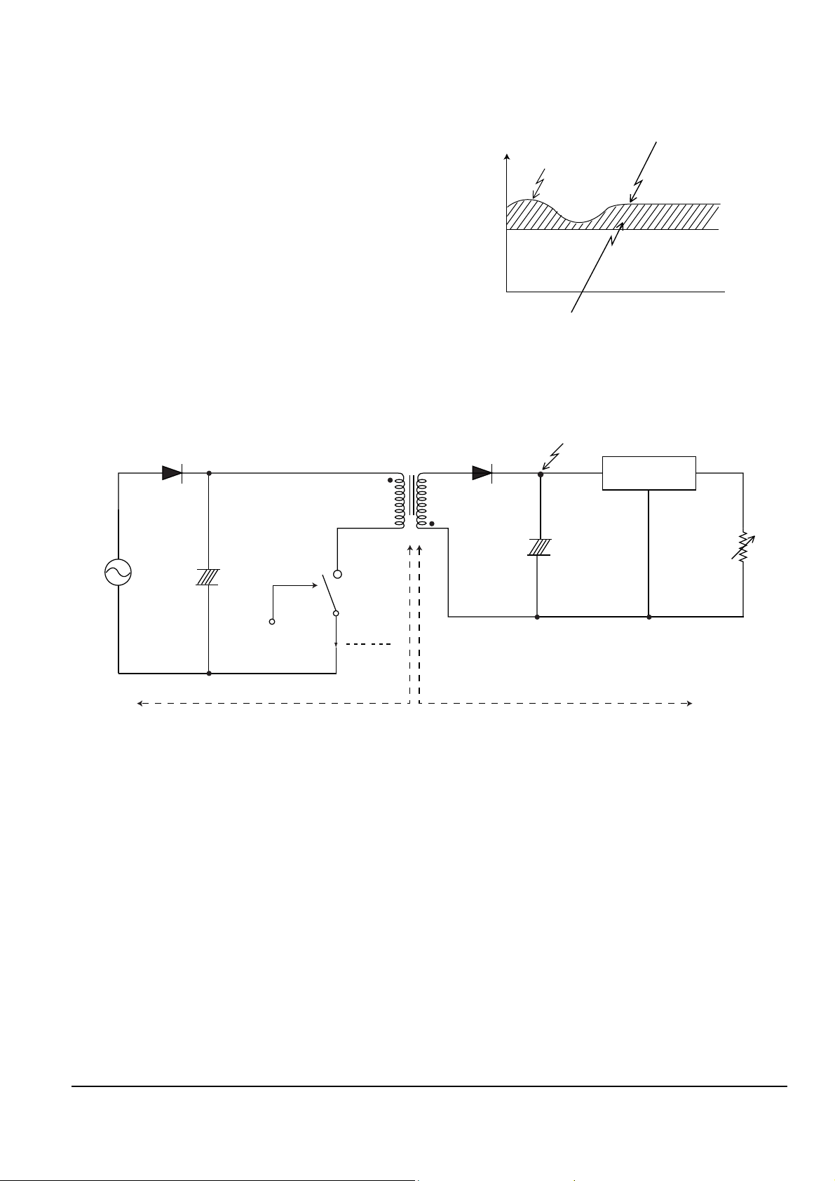
Little noise because the output waveform of transformer is
sine wave.
b. Disadvantages :
È Additional margin is required because Vs is changed
(depending on power source). (The regulator loss is
caused by margin design).
È Greater core size and condensor capacity are needed,
because the transformer works on a single power
frequency.
Fig. 2-5
2-1-1 (B) SMPS(PULSE WIDTH MODULATION METHOD)
Fig. 2-6
3 Terms
- 1st : Common power input to 1st winding.
- 2d : Circuit followings output winding of transformer.
- f(Frequency) : Switching frequency(T : Switching cycle)
- Duty : (Ton/T) x 100
V
Vreg
Vout
0 t
Change by common power
Regulator loss
Transformer Vout
(Np)
(Vp)
Switch
Vs switch
I switch
Vin
ON/OFF Control
+
–
+
–
+
+
+
–
(Vs)
(Ns)
Regulator
Reference Information
Samsung Electronics 2-3
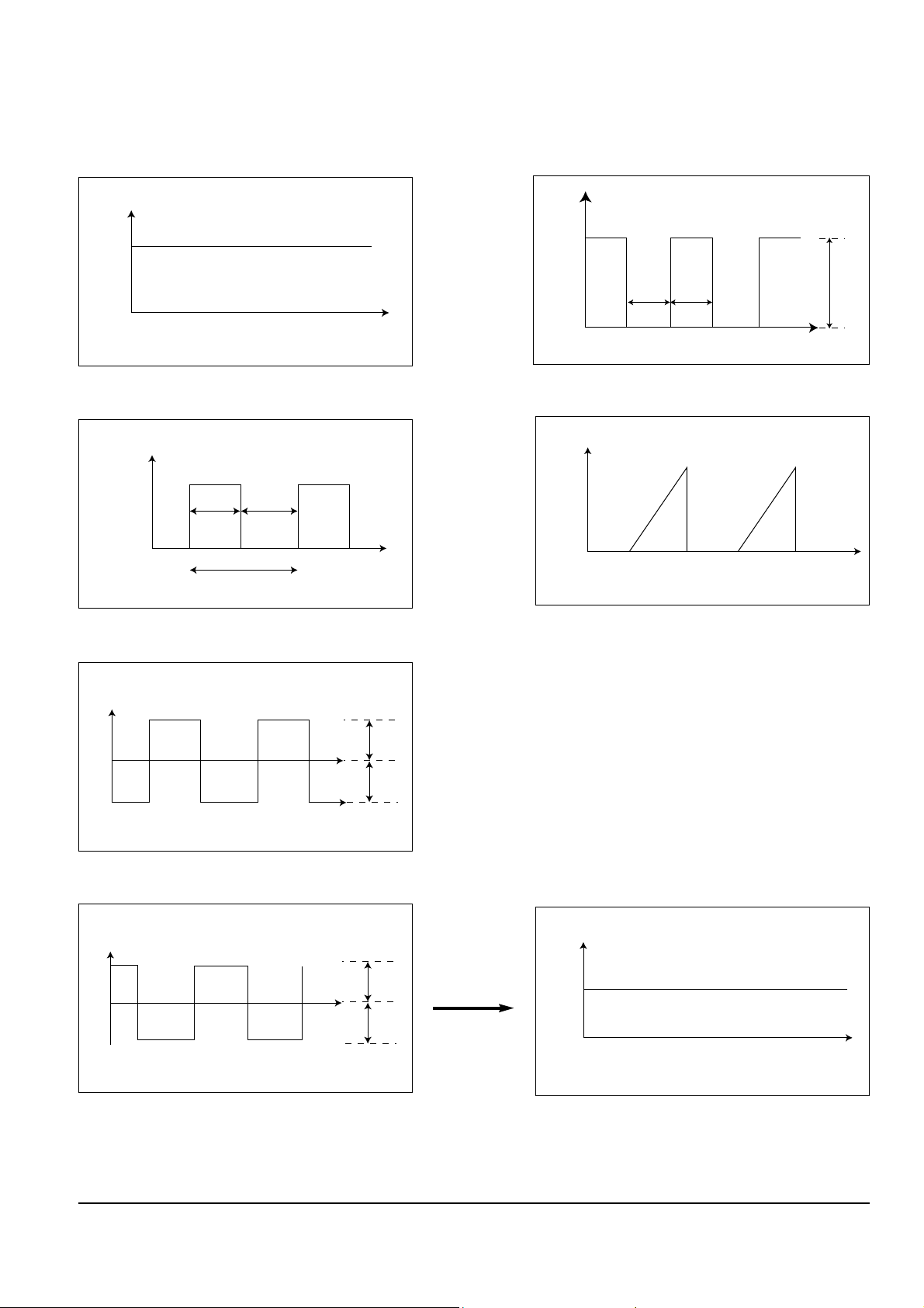
3 Waveform
Fig. 2-7 Fig.2-11
Fig. 2-8 Fig. 2-12
Fig. 2-9
Fig. 2-10 Fig. 2-13
Vin
0
t
Vswitch
ON/OFF
Control
Vp
0
Ton
Toff
0
Vin–Vp
t
Iswitch
Ton Toff
0
f t
0
t
Vin
t
Vps
Vs
0
Vs1
t
Vs2
Vout
0
t
Reference Information
2-4 Samsung Electronics
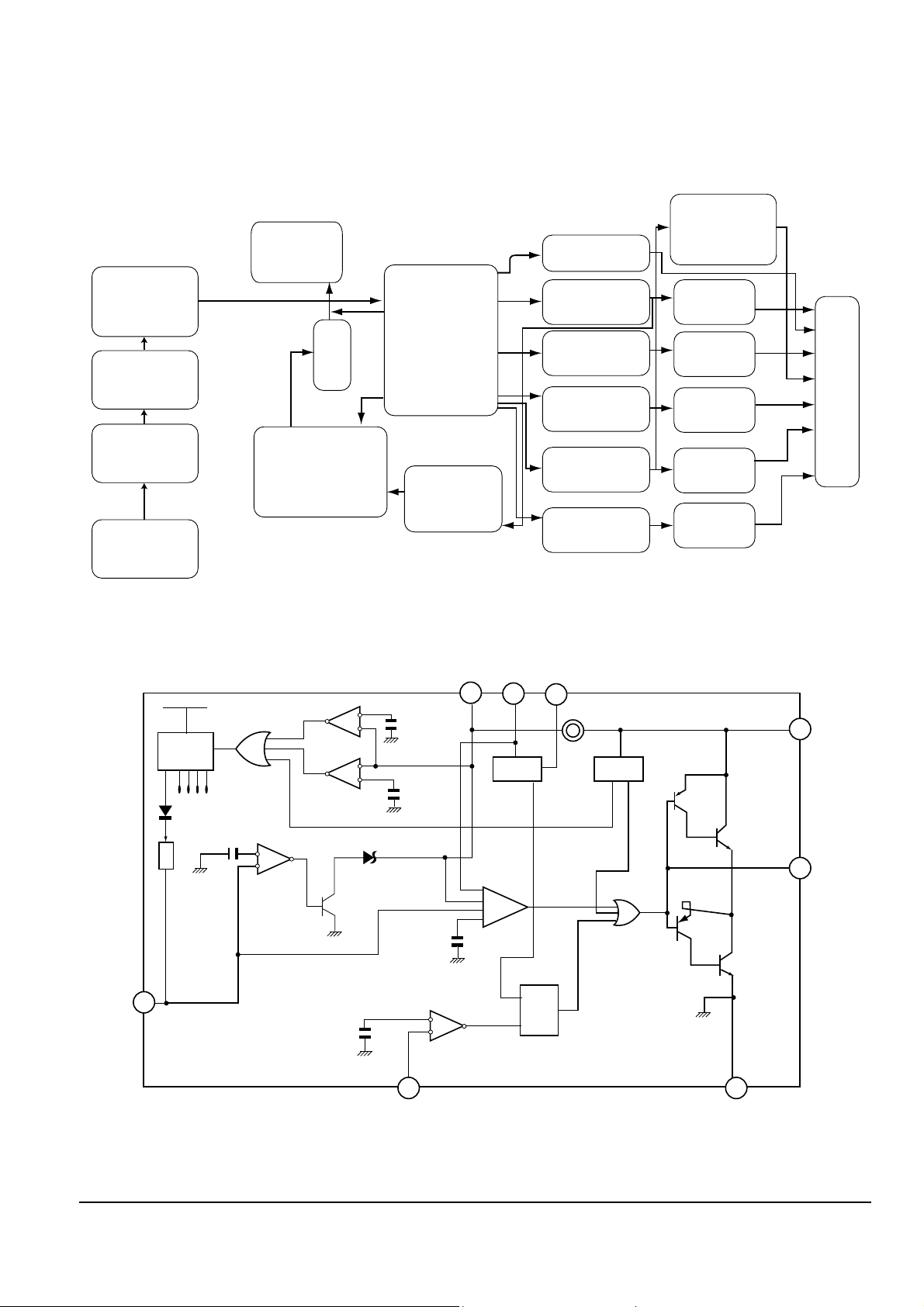
2-1-1(c) INTERNAL BLOCK DIAGRAM
1. Internal block diagram of SMPS circuit
Fig. 2-14
2. PIC1(KA7552) internal block diagram
Fig. 2-15
BIAS
OFF
2.8V
7.0V
CS
8 7
1
CT RT
10UA
OSC UVLD
VCC
OUT
GNDIS(+)
PB
4.3k
3.6V
ZD
G
D MAX
(46%, 70%)
R
S
Q
PWM
OCP
+
Ð
Ð
+
Ð
+
Ð
+
0.24V
6
5
4
3
2
Noise removing circuit at
power
input/output
Noise
removal
(SNUBBER)
Smoothing
circuit
Rectified circuit
Line filter
Power IN
(85-265V)
F
E
T
FLT driving
circuit
5V rectified
smoothing circuit
3.3V rectified
smoothing circuit
Convertor
PWM control circuit
(KA7552)
Voltage
detection
circuit
9V rectified
smoothing circuit
8V rectified
smoothing circuit
-8V rectified
smoothing circuit
5V rectified
voltage
circuit(x2)
3.3V rectified
voltage
circuit
9V rectified
voltage
circuit
8V rectified
voltage
circuit
-8V rectified
voltage
circuit
O
u
t
p
u
t
Reference Information
Samsung Electronics 2-5
2-1-2 SMPS circuit description
2-1-2(a) CIRCUIT METHOD
FLY-BACK PWM(Pulse width modulation) control
2-1-2(b) CIRCUIT DESCRIPTIONS
1. AC power rectification/smoothing terminal
- PD01 : Convert AC power to DC(Wave rectification)
- PO10 : Smooth the voltage converted to DC(Refer to Vin of Fig. 2-7)
- PC01, PC02, PC03, PC04, PC05, PC06, PL01, PL02, PL03 : Noise removal at power input/output
- PVA1 : SMPS protection at power surge input
- PVA2 : SMPS protection at 2st ground surge input(PVA1 pattern open : to remove noise)
- PR10 : Rush current limit resistance during power cord insertion.
È Rush current = (AC input voltage x 1.414 - Diode drop voltage) / Pattern resistance + PL02.01
resistance + PC10 resistance + PR10) (AC230V based : approx. 26A)
È Without PR10, the bridge diode might be damaged as the rush current increases.
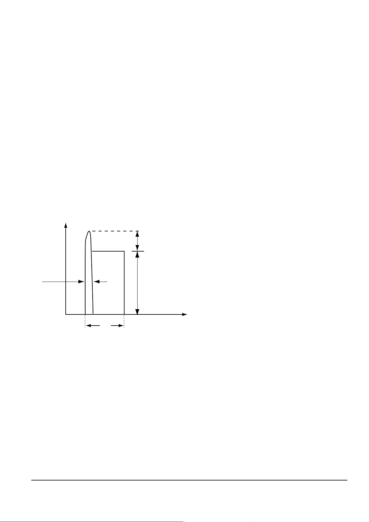
2. SNUBBER circuit : PR17, PR18, PC11, PD10
- Prevent residual high voltage at the terminals of
switch during switch off/Suppress noise.
High inverted power occurs at switch off,
because of the 1st winding of transformer:
(V=L1xdi/dt. LI : Leakage Induction)
A very high residual voltage exists on both
terminals of PQ1 because dt is a very short.
- SNUBBER circuit protects PQ1 from damage
through leakage voltage suppression by RC,
(Charges the leakage voltage to PD10 and PC11,
and discharges to PR17 and PR18).
- PC12, PL11 : For noise removal
Fig. 2-16
3. PIC1 Vcc circuit
- PR11, PR12, PR13, PR14 : PIC1 driving resistance (PIC1 works through driving resistance at power cord in)
- PIC1 Vcc : PR20, PD12, PC17
1) Use the output of transformer as Vcc, because the current starts to flow into transformer while PIC1 is active.
2) Rectify to PD12 and smooth to PC17.
3) Use the output of transformer as PIC1 Vcc : The loads are different before and after PIC1 driving.
(Vcc of PIC1 decreases below OFF voltage, using only the resistance due to load increase after PIC1 driving.)
- PR20 : For noise removal
0
Vin–Vp
Vswitch
dt
Toff
t
Inverted power
by leakage
inductance

Reference Information
2-6 Samsung Electronics
4. PIC1 function : PWM control (Refer to Switch ON/OFF Control of Fig. 2-6)
- 0.56V
- -
OFF voltage 0.75V
SHUT OFF voltage 2.8V
DUTY MAX voltage 2.3V
LIMIT voltage 0.24V
- -
- -
Maximum DUTY 70%
ON voltage 16V
OFF voltage 8.7V
- -
OFF voltage 0.42V
ON voltage 0.56V
3.6V
SHUT OFF voltage 7V
MAX DUTY voltage 2.3V
1 RT
2 F/B
3 IS
4 GND
5 OUT
6 VCC
7 CT
8 CS
PIN NAME CLASS SPEC. FEATURES
* Resistance to determine OUT terminal(pin5) ON/OFF control frequency
- Determined with CT terminal(pin7) and for DVDP, 50KHz
RT : PR24, CT : PC13
* OUT terminal duty is determined by F/B potential
(Duty control : 2st output constant-voltage control)
* The voltage of PIC2(Output voltage freedback) is input to F/B terminal.
* If F/B terminal potential decreases below 0.75V, OUT duty is zero.
- SMPS 2st output voltage is zero.
* If F/B potential is above 2.8V, CS terminal(8pin) potential ascends in IC.
If CS potential rises above 7V, SHUT OFF mode is maintained.
* SHUT OFF mode : IC internal bias OFF state.(Operation stop)
* If IS terminal potential is above 0.24V, maintain on time only when IS
terminal potential is 0.24V without holding OUT duty determined in F/B
terminal(Duty limit).
* PQ1(F,E,T) current is distributed to PR22, PR21 in voltage, and input to IS
terminal.
* Purpose : Limit the overcurrent of PQ1(Current waveform : See Fig. 2-10)
* Ground(SMPS 1st ground)
* ON/OFF control pulse output terminal(f : fixed, ON TIME : variable)
* Maximum duty is 70% (Maximum).
* IC power supply terminal. IC function starts at exceeding 16V. Vcc less than
8.7V will be OFF after IC working.(See Clause 3. Vcc circuit)
- Vcc voltage is 10-12V at normal operation.
* ON/OFF frequency determining terminal(Refer to 1 pin RT terminal)
* OS potential setting : Connect the condenser to OS terminal(PC14)
* ON/OFF control : If CS potential is above 0.56V, IC function starts and if
below 0.42V, IC function stops.
* At normal operation : Maintain 3.6V in IC
* SHUT OFF mode : If CS potential is above 7V, shut off.(Overload
prevention)
- SHUT OFF function : When IS, F/B, CS terminal are all operated normally.
(Refer to Clause 6. MAX. POWER limiting circuit)
* SOFT START : Switch protection at initial starting
- F/B potential is 3.6V internally at initial starting.(Duty max.)
- PQ1 damage occurs due to overcurrent on switch at duty max.
- CS terminal sets the duty with F/B terminal
- Connect PC14 to CS terminal and set the voltage charging time at initial
starting.
- Increase the duty by raising the voltage gradually via PC14 at initial starting
for normal operation.
(Duty max. is limited by F/B potential at initial starting)
Normal operation
voltage
Reference Information
Samsung Electronics 2-7
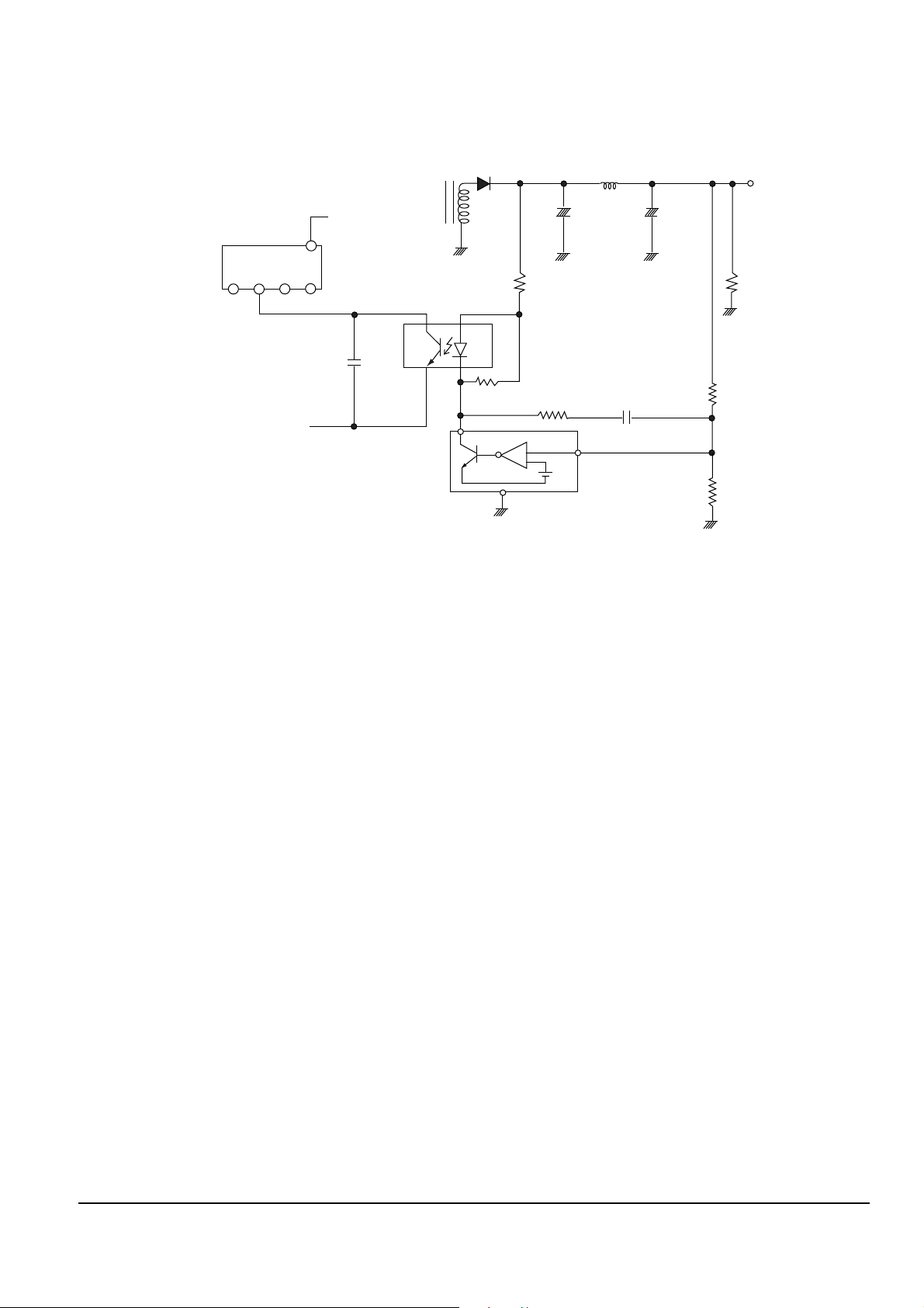
5. Feedback control circuit
Fig. 2-17
- F/B terminal of PIC1 determines output duty cycle.
- Duty definition : Refer to Vs1 in Fig4-10.(Duty up: Vs1 up, Duty down: Vs2 down)
- C-E(Collector-Emitter) of PIC2 and F/B potential of PIC1 are same.
- At F/B terminal open : SHUT OFF mode
È F/B potential is set to 3.6V internally.
F/B potential decreases to 1-2V by C-E voltage of PIC2 ( controlled by normal
operation. )
È When F/B terminal is open, shut off occurs because 2.8V is exceeded.
(Refer to clause 4.)
3 Operation descriptions
a. Internal OP-Amp Ô+Õ base potential of PIC3 is 2.5V and external Ò-Ó input potential is connected with PR38
and PR39 to maintain Vout of 5.8V. (Vout = ((PR36 x PR39) / PR39) x 2.5V)
b. If load of 5.8 V terminal increases(or AC input voltage decreases) and Vout decreases below 5.8V, then :
PIC3 ÔPÕ potential down below 2.5V --> PIC3 A-K of base current down --> PIC3 of A-K current down -->
PIC2 Diode current down --> PIC2 C-E current down --> PIC2 C-E voltage up --> PIC1 F/B voltage up -->
OUT Duty up --> Transformer 1st current up --> Transformer 1st power up --> Vout up --> Maintain
Vout 5.8V
c. If load of 5.8 V terminal decreases(or AC input voltage rises) and Vout rises above 5.8V, then :
Reverse sequence of the above description ® Duty down ® Vout down ® Maintain 5.8V
(i.e., the feedback to maintains 5.8V).
- PR35, PR36 : Reduce 5.8V overshoot
- PR37, PC43 : Prevent IC3 oscillation(for phase correction)
- PC18 : Adjust feedback response rate
PIC1
OUT
ON/OFF Control
Trans
PC18
PIC2
C
E
A
P
K
2.5V
K
PR36
PR37
A
PR35
PC38 PC39
PR40
100/2W
PL37
5 .8V
PD35
PC43
PR38
PR39
GND
++ ++
GND
F/B
1
2
3
4
5
PIC3
-
+
Reference Information
2-8 Samsung Electronics
6. Maximum power limit circuit
* Circuit configuration : PIC1 F/B, CS, IS terminal PR23, PR21,
PR22, PC13A
* Role : Switch overcurrent protection
* The current on switch inputs to IS and outputs as voltage via
PR23, PR21, PR22.
* If the current on switch increases and IS terminal input
voltage exceeds 0.24V, duty is determined by F/B terminal.
Accordingly, the current on switch is limited less than specific
current.(If 2d load rises, the switch current increases. Refer to
clause 5. in circuit description).
* If I/S terminal is open : Switch and other parts are damaged
because the switch is not limited during abnormal status (for
example, 2d ouput terminal short).
Fig. 2-18
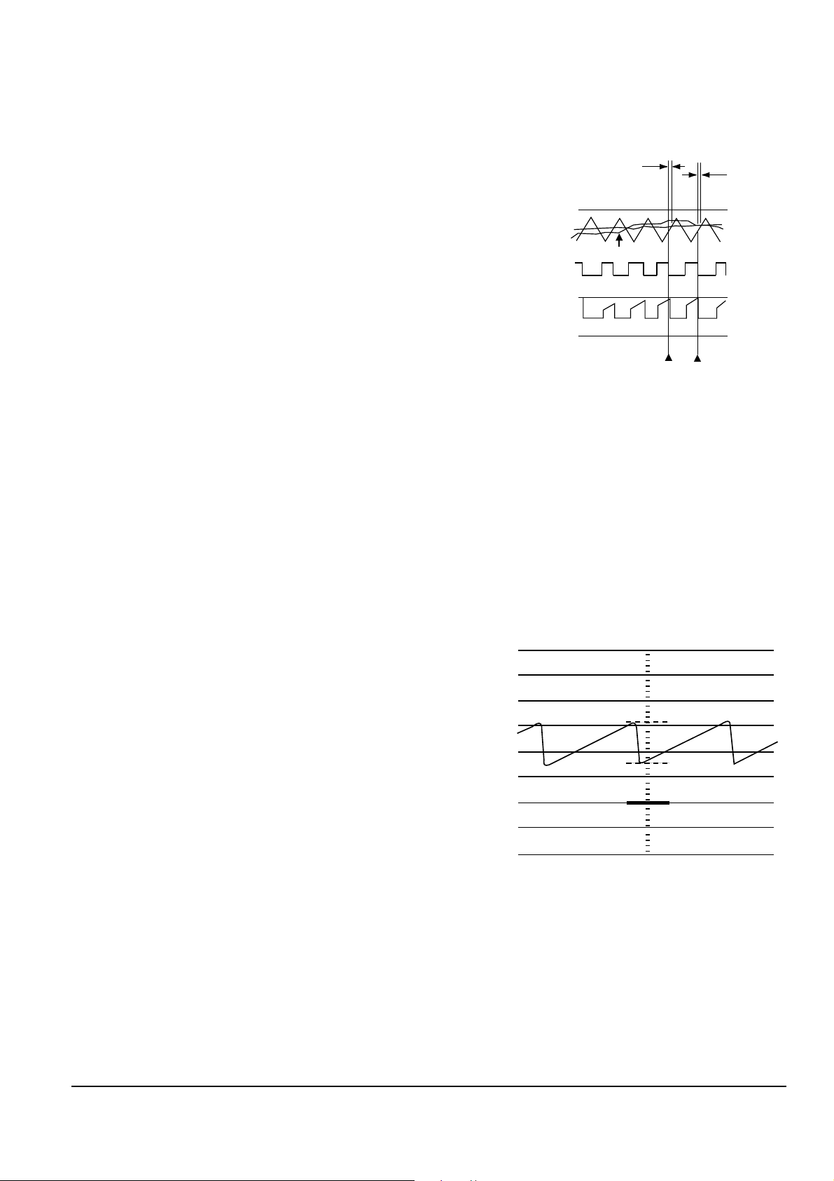
1) Intermittent operation mode
- Definition : PIC1 canÕt deliver normal output, and repeats Vcc ON/OFF operation(Vcc voltage is swing
between 16V(ON) and 8.7V(OFF).
- Operation description : for example. 2d output terminals shorted, then :
Specific 2d terminal short --> 2d power is concentrated on short terminal --> 5.8V(PC39)
voltage down --> F/B voltage up (Refer to clause 5.) --> Duty up --> Switch current up --> Limit switch
current to IS terminal(Duty limit) --> Apply 1st supply power in comparison with 2d power -->
Concentrate on 2d power short terminal --> PIC1 Vcc terminal TRANS. output voltage down below
8.7V --> PIC1 OFF --> PIC1 ON via driving resistance --> Above operations repeated ® Maintain
intermittent operation mode (See Fig. 2-19 Waveform).
At short release : normal operation
2) Short OFF mode
- Main examples : Feedback circuit Open, Max, Power
excess(Design spec.), 5.8V Terminal short
- Operation description :
Ex - 2d load is high abnormally;
1st supply power is low in comparison with 2d output power.
5.8V down --> Duty up --> Switch current up -->
IS terminal duty limit --> 1st supply power limit --> 5.8V
voltage down --> F/B potential above 2.8V(Shut OFF voltage)
--> OS terminal potential up (Refer to Clause 4.)F/B -->
OS potential above 7V --> Shut OFF mode
- The output voltage of SMPS is zero because PIC1 doesnÕt work
during Shut OFF mode.
- Shut OFF mode release : OS potential decreases below
7V.(Charge OS terminal forcely)
- Feedback terminal open : Shut OFF (Refer to clause 5.);
PC13A : For IS terminal input noise removal Fig. 2-19
CS Voltage(3.6V)
Duty Limit sector
FB Voltage
DT Voltage
OSC OUT
OUT Voltage
COM.C4(0.24V)
Over current protection
Over current protection
Blas voltage
IS(+) Voltage
Time : 100ms / div
Volt : 5V / div
16V
8V
GND

Reference Information
Samsung Electronics 2-9
7. Shut Off mode prevention circuit at instant load increase : PC15, PZD13
- During a sudden load increase;
By means of current concentration on specific output terminal, 5.8V voltage down --> F/B potential up -->
Maintain Shut Off mode.
Stablize F/B potential (Loading completion) below 7V by lengthening CS potential rise time to 7V
(in order to prevent Shut Off mode).
- Normal operation : CS potential is 3.6V and PZD13(4.7V ZENER) is open.
- OD potential above 4.7V at instant load increase --> PZD13, PC15 work --> OS terminal condenser capacity
increases in parallel with PC14 and PC15 --> CS potential rising rate down --> Instant operation completed
--> F/B potential stable --> Normal operation
8. Maximum power limiting circuit addition : PZD11, PR19
- SMPS efficiency : Below 25W : High efficiency at AC110V input
Above 25W : High efficiency at AC230V input
- The peak value of current on switch at overload is lower than that at 110V input because SMPS is highly
efficient above 25W at 230V input. Therefore, maximum power increases at 230V as compared to
110V at overload. Add PZD11, PR19 and set to the same level as 110V.
- Higher at 230V input than at PZD11 input, limit maximum power because IS terminal potential goes up.
9. PQ1(F,E,T) Gate Drive Circuit : PR15, PR16, PD11
- PIC1 OUT is square wave but charging and discharing by PR15, PR16 occurs due to internal condenser
between gate-sources of PQ1.
- PR15, PR16 : Switch ON Time setting - PD11 is reverse : PIC1 OUT --> PR15 --> PR16 --> Charge to gate
- PR16, PD11 : Switch OFF Time setting - PD11 is proper : GATE - PR16 --> PD11 --> Discharge to PIC1
OUT(GND)
- Switch ON/OFF time : Releated to switch loss and noise
10. PIC1 overcurrent protection : PZD12
- Operate PZD12 and protect PIC1 from damage from residual overcurrent (PIC1 Vcc, due to external surge
inflow and feedback line open).
2-10 Samsung Electronics
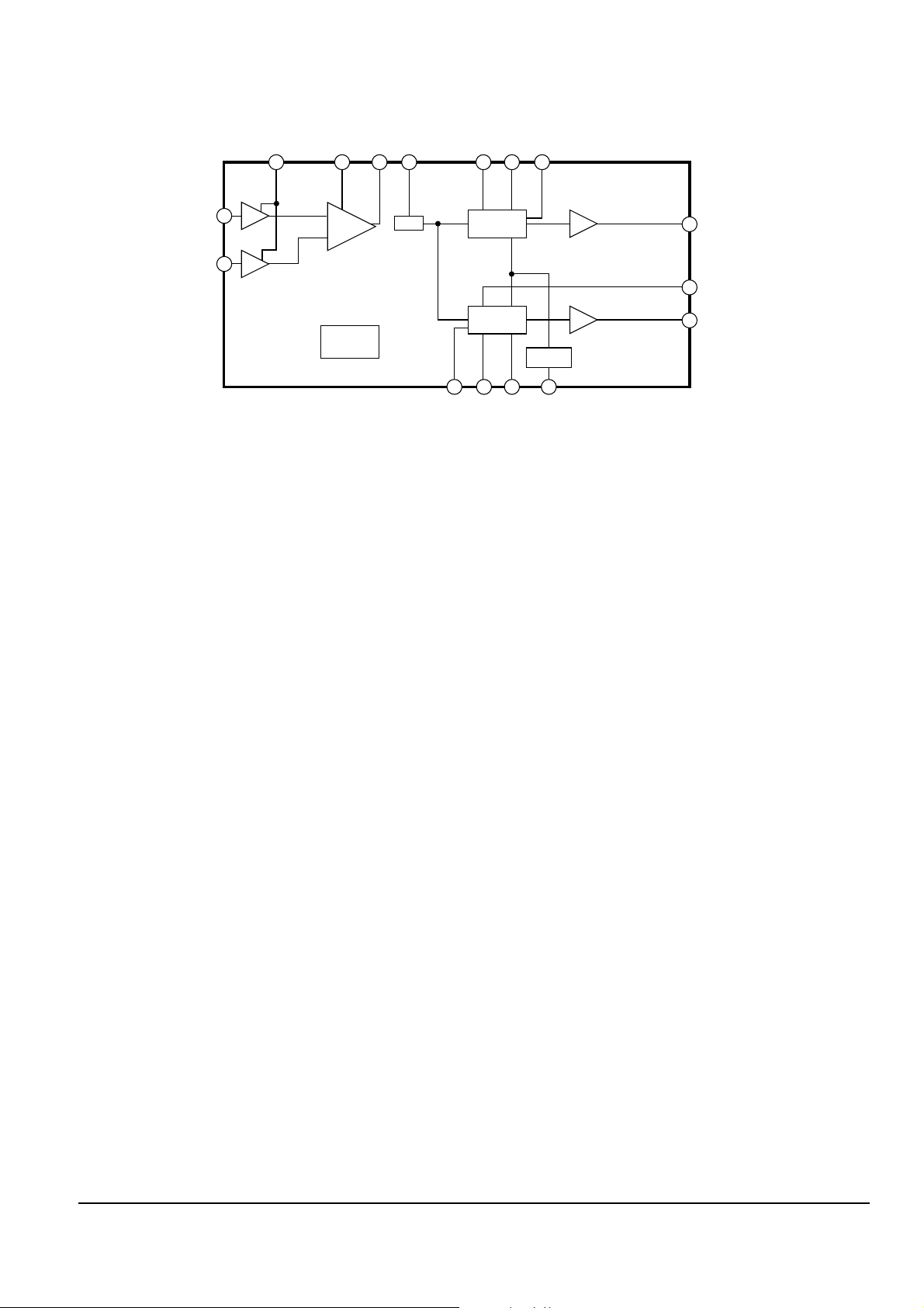
2-2-1 RIC1(TA1236F)
TA1236F is combined with TA1253FN, TC9240F and TC90A19F as bipolar IC developed for DVD SERVO system.
Main features include DVD waveform equalizing, CD waveform equalizing, focus error signal generation, 3-beam
tracking error signal generation, laser power control, etc. after receiving the pick-up output converted into I/V.
1. Basic potentiometer
TA1236F uses a single power method and each circuit is based on VREF of 2.1V. Note :
symmetrical about GND for VREF because VREF(pin20) terminal is needed for IC, which uses the peripheral VREF
and 2VREF output(pin18).
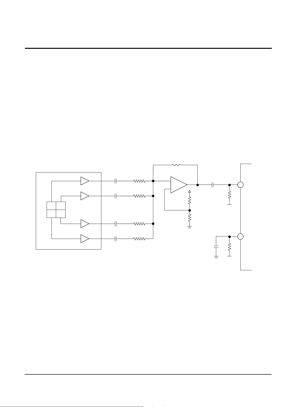
2. RF signal
Fig. 2-20 shows the flow of signal generated by the pick-up.
A, B, C, D signals detected from pick-up are converted in to RF signal(A+B+C+D) via RF summing AMP.
RF signal is inputted to RFN(pin55) among input terminals and RFP(pin54) is used for AC ground.
Fig. 2-20
Fig. 2-21 shows the waveform-equalizing block diagram for the RF signal.
It outputs to EQout(pin 46) terminal by initially changing switching AMP gain of DVD and CD, and then
adjusting the level in VCA. It controls VCA gain by means of RF gain(pin 48) and interfaces with PWM signal,
(output from RFGC terminal of TC9420F, via low-pass filter to constitute a loop for adjustment of constant
amplitude). The gain in EQout is 1.0 for DVD and 1.67 for CD.
EQout terminal is connected with EQin(pin 45) externally, and inputs into DVD EQ and CD EQ(Waveform
equalizing circuit).
55
54
PICK-UP
PD
D A
C B
I-V AMP
RC12
104
RR20
1K
RC10
104
RR19
1K
+
–
RC15
104
RR24
1K
RC14
104
RR22
1K
RR18
1.2K
RIC3 OPA 650
SUMMING AMP
2
3
6
RC11
104
RR23
10K
RR50
5.6K
RR51
5.6K
RC22
104
RR33
10K
Vref
RIC1
TA1236
RFN
Vref
RFP
+5A
2-2 RF circuit description
Reference Information
Reference Information
Samsung Electronics 2-11
Fig. 2-21
The control parameters of DVD EQ and CD EQ are as follows.
1) DVD EQ control parameter
- DVDEQ(pin 43) : Changes the gain of peak frequency with EQ frequency characteristic. Convert PWM
signal, output from TC90A19F, into DC via low-pass filter.
- DVDTIME(pin 41) : Changes the peak frequency with EQ frequency characteristic. Convert PWM signal,
output from TC90A19F, into DC via low-pass filter.
- S/Dse1(pin 64) : Changes the peak frequency (like DVD TIME) as 2d control. ( Switched according to
regeneration speed ratio of single/double layer).
- MCK(pin 15) : Input the base clock and link the peak frequency with it. The amplitude of MCK might be
small (500mVp-p).
- DVDGD(pin 25) : Changes the group delay characteristics with EQ frequency characteristic.
2) CD EQ control parameter
- CD EQ(pin 40) : Changes the gain of peak frequency with EQ frequency characteristic. The constant DC is
supplied to a resistive voltage divider.
- CD TIME(pin 42) : Changes the peak frequency with EQ frequency characteristic. The constant DC is
supplied to a resistive voltage divider.
- S/Qse1(pin 44) : Changes the peak frequency (such as CD TIME) as 2d control. (Switched according to play
linear velocity ratio of quadruple/single rate. Set to Ô0Õ because only one rate is vaild in
this system).
Note : CD and DVD signals are equalized according to the above control parameters ,and then output to CD
EQ OUT (pin39) and DVD EQ OUT (pin34). Then, CD signal is transferred to TC9420F, DVD signal is
sent to TC90A19F and detected.
DVDsel RFgain EQout EQin
CDEQCD
TIME SQsel
RFN
RFP
47 48 46 45 40 42 44
55
54
64 41 43 15
34
25
39
VCA
ATT
CD EQ
DVD EQ
RIC1
TA1236F
GEN.
T/CON
SDsel DVD
TIME
DVDEQMCK
DVD G/D
DVD EQ OUT
CD EQ OUT
2-2-2 Description of data processor for DVD
(Including DIC1 and DIC5 protection IC)
1. Outline
The data processor IC for DVD does the following :
1) Converts RF signal to digital, demodulates original signal and corrects errors,
2) PLL circuit to generate the clock for data detection in accordance with play velocity,
3) CLV control circuit to control the rotation rate of disc,
4) DIC5 Protection IC, connected with input/output of data processor, which releases the protection for the
protected data (which is then transmitted to video decoder and Micom).

Reference Information
2-12 Samsung Electronics
2. Operation
1) Input circuit
RF data equalized in RF stage is AC-coupled via pin 50 and input as 2.1Vpp. Then, the bias voltage becomes
1.65V by means of DC bias in IC.
2) PLL circuit
The input data generates the clock necessary for the PLL circuit. PLL circuit for clock generation generates
the phase error signal through RLLD (pin 38), PDOP (pin 37), PDON (pin 36). The loop filter consists of
built-in OP Amp and external parts.
The RLLD signal occurs only when the velocity difference between clock and data is large, and it sets the PLL
oeprational velocity. RLLD signal doesnÕt occur at normal play except during searches
3) Data slicer
As the PLL generates the clocks, the slice circuit converts the analog signal to digital. that is, it switches to 1
if greater than regular reference voltage, and to 0 if less. The sliced signal may be observed at pin 34 (ED7)
with a scope. If the signal has an error, it is necessary to check that the bias of input RF signal is correct, as
well as the condensor at pin 42 (SLCO).
4) CLV circuit]
The signal is input to the circuit which generates DMO and CLV signals to control the rotation of the spindle
motor. The control signal is output via pin 54(DMO). Then, the output signal is the 3d signal (a pulse derived
from the midpoint voltage). If an error occurs in spindle motor during DVD play, check this signal.
5) Modulation and ID. Sync detection
The signal is synchronized, using the generated clocks, and Sync. signal is detected through Sync. signal
detection circuit for modulation and all other signal processes. Sync. signal canÕt be observed externally, but
the interrupt at each 1.4ms cycle may be checked on pin 23 (during normal detection, the interrupt signal is
generated periodically). It is difficult to precisely define 1.4ms cycle, because other interrupts are also
occuring.
During Sync. detection, the recorded signal is converted to data by means of an 8/16 modulation circuit.
The modulated signal is saved in memory, and interfaced externally for error correction.
7) Error correction circuit]
The data saved in external buffer memory after modulation are read by data processor sequentially for error
correction. The data with all corrections are output by request of the next stage (video decoder).
8) VBR buffering]
The disc jumps the track repeatedly on waveform while checking each signal during normal play of DVD
because it uses the VBR method (completely different from existing CD, video CD, etc). VBR play method
enhances the data efficiency to improve the screen quality twofold, by using additional data for complex
video and less data for simple video at compression. It saves the data in memory, and if the memory is full, it
stops the play instantly to reset. If the data is removed, it repeats play because the play velocity varies
according to data compression ratio. This process is known as VBR, and the used memory is known as the
track buffer (or VBR buffer). A 4MIT DRAM attached to data processor includes this function.
9) Protection circuit]
Read if protected, and key for protection release from Read-in area (starting at first disc play). These
operations are performed by TC6804 automatically.
Protection IC is located between output of data processor and input of video decoder, (the next stage).
it decodes the protected data after recognizing the key information read from disc and data status. If a disc
violates the protection method, it stops the operation and reports to Micom.

Reference Information
Samsung Electronics 2-13
2-3 System control circuit description
2-3-1 Outline
The main micom peripheral circuit is composed of 16bit Micom, 2M EPROM for Microcord and data save, 1M
SRAM for data read/write on running, 512 byte EEPROM for permanent storage of data needed at power off,
MIC4(74AC573) to latch only address in the bus where address and data are mixed, address decoder for selection
of external device chip and 20MHz clock oscillator for micom operation. The micom(MIC1, TMP93CS41) mounted
in main board analizes the key commands of front panel or instructions of remote control through communication
with micom(FIC1, LC86P6232) of front and controls the devices on board to execute the corresponding commands
after initializing the devices connected with micom on board at power on.
 Loading...