


SAMSUNG DVD_709-707 Service Manual Cover
DVD PLAYER
DVD-
909
DVD-
709
SERVICE
1. Precautions
2. Reference Information
3. Product Specification
4. Operating Instructions
5. Disassembly and Reassembly
6. Circuit Descriptions
7. Troubleshooting
8. Exploded Views and Parts List
9. Electrical Parts List
10. Block Diagrams
11. PCB Diagrams
12. Wiring Diagram
13. Schematic Diagrams
Manual
DVD PLAYER CONTENTS
SERVICE MANUAL DVD-909/709
OPEN/
CLOSE
POWER
STANDBY
PHONE
ADVANCED DOLBY DIGITAL DECORDER BUILT-IN
LEVEL
SKIP
MIN MAX
OPEN/
CLOSE
OPEN/
CLOSE
DIGITAL VIDEO
SPATIALIZER
N-2-2
OPEN/
CLOSE
STANDBY
OPEN/
CLOSE
24bit 96kHz AUDIO D/A CONVERTER
DIGITAL VIDEO
SPATIALIZER
N-2-2
DVD/VIDEO-CD/CD PLAYER DVD-909
DVD/VIDEO-CD/CD PLAYER DVD-709
POWER
SKIP
DVD-709
DVD-909
ELECTRONICS
© Samsung Electronics Co., Ltd. MAY. 1999
Printed in Korea
AH68-00137A
Samsung Electronics 1-1
1. Precautions
1-1 Safety Precautions
1) Before returning an instrument to the customer,
always make a safety check of the entire instrument,
including, but not limited to, the following items:
(1) Be sure that no built-in protective devices are
defective or have been defeated during servicing.
(1)Protective shields are provided to protect both
the technician and the customer. Correctly replace
all missing protective shields, including any
remove for servicing convenience.
(2)When reinstalling the chassis and/or other assembly in the cabinet, be sure to put back in place
all protective devices, including, but not limited to,
nonmetallic control knobs, insulating fish papers,
adjustment and compartment covers/shields, and
isolation resistor/capacitor networks. Do not operate this instrument or permit it to be operated without all protective devices correctly installed and
functioning.
(2) Be sure that there are no cabinet openings through
which adults or children might be able to insert
their fingers and contact a hazardous voltage. Such
openings include, but are not limited to, excessively wide cabinet ventilation slots, and an improperly fitted and/or incorrectly secured cabinet back
cover.
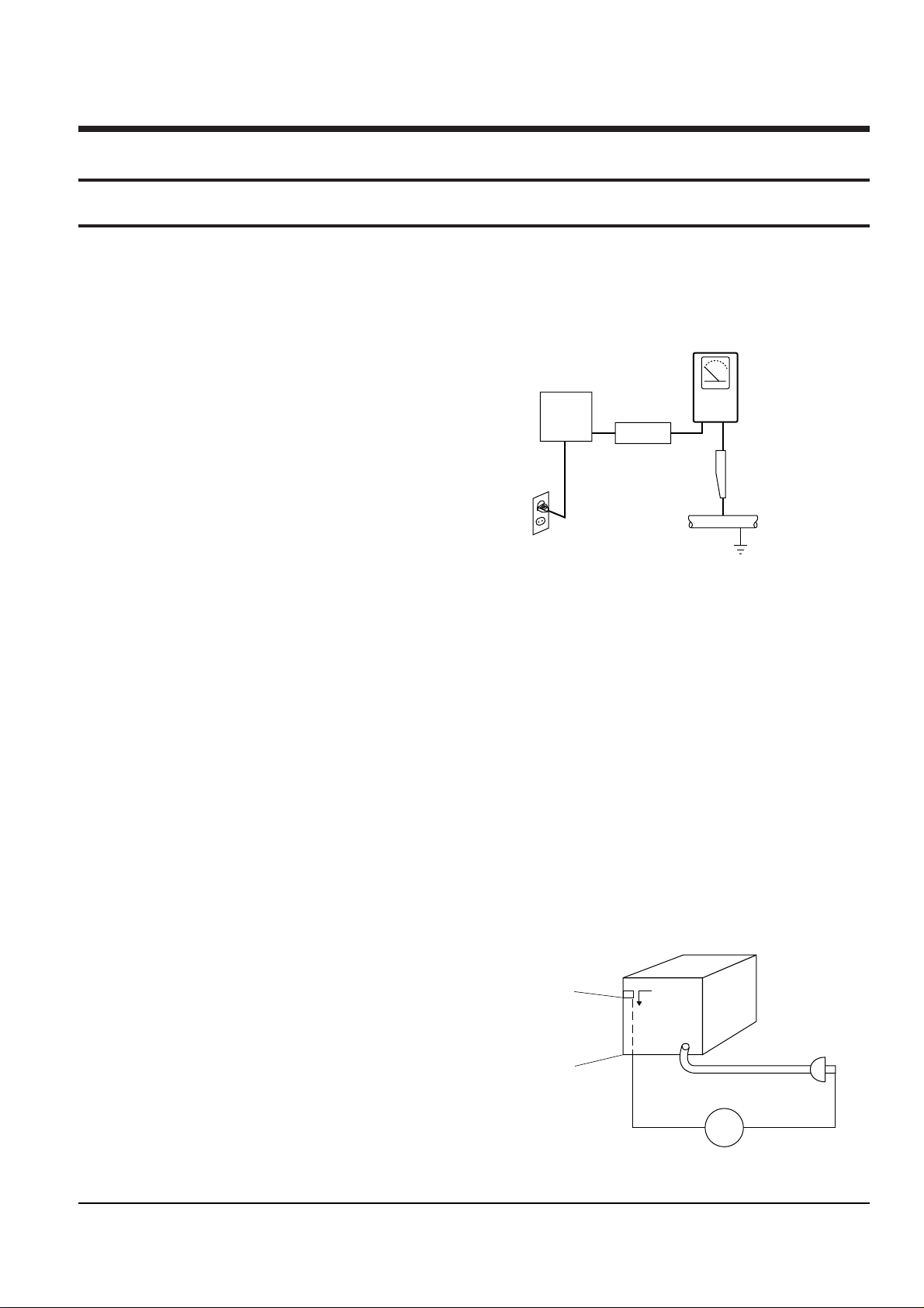
(3) Leakage Current Hot Check-With the instrument
completely reassembled, plug the AC line cord
directly into a 120V AC outlet. (Do not use a isolation transformer during this test.) Use a leakage
current tester or a metering system that complies
with American National Standards institute (ANSI)
C101.1 Leakage Current for Appliances and
Underwriters Laboratories (UL) 1270 (40.7). With
the instrumentÕs AC switch first in the ON position
and then in the OFF position, measure from a
known earth ground (metal water pipe, conduit,
etc.) to all exposed metal parts of the instrument
(antennas, handle brackets, metal cabinets, screwheads, metallic overlays, control shafts, etc.), especially any exposed metal parts that offer an electrical return path to the chassis.
Any current measured must not exceed 0.5mA.
Reverse the instrument power cord plug in the outlet and repeat the test. See Fig. 1-1.
Any measurements not within the limits specified
herein indicate a potential shock hazard that must
be eliminated before returning the instrument to
the customer.
Fig. 1-1 AC Leakage Test
(4) Insulation Resistance Test Cold Check-(1) Unplug
the power supply cord and connect a jumper wire
between the two prongs of the plug. (2) Turn on the
power switch of the instrument. (3) Measure the
resistance with an ohmmeter between the
jumpered AC plug and all exposed metallic cabinet
parts on the instrument, such as screwheads,
antenna, control shafts, handle brackets, etc. When
an exposed metallic part has a return path to the
chassis, the reading should be between 1 and 5.2
megohm. When there is no return path to the chassis, the reading must be infinite. If the reading is
not within the limits specified, there is the possibility of a shock hazard, and the instrument must be
re-pared and rechecked before it is returned to the
customer. See Fig. 1-2.
Fig. 1-2 Insulation Resistance Test
DEVICE
UNDER
TEST
(READING SHOULD
NOT BE ABOVE
0.5mA)
LEAKAGE
CURRENT
TESTER
EARTH
GROUND
TEST ALL
EXPOSED METER
SURFACES
ALSO TEST WITH
PLUG REVERSED
(USING AC ADAPTER
PLUG AS REQUIRED)
2-WIRE CORD
Antenna
Terminal
Exposed
Melal Part
ohm
ohmmeter

Precautions
1-2 Samsung Electronics
2) Read and comply with all caution and safety related notes non or inside the cabinet, or on the chassis.
3) Design Alteration Warning-Do not alter of add to
the mechanical or electrical design of this instrument. Design alterations and additions, including
but not limited to, circuit modifications and the
addition of items such as auxiliary audio output
connections, might alter the safety characteristics of
this instrument and create a hazard to the user. Any
design alterations or additions will make you, the
service, responsible for personal injury or property
damage resulting therefrom.
4) Observe original lead dress. Take extra care to
assure correct lead dress in the following areas:
(1) near sharp edges, (2) near thermally hot parts (be
sure that leads and components do not touch thermally hot parts), (3) the AC supply, (4) high voltage,
and (5) antenna wiring. Always inspect in all areas
for pinched, out-of-place, or frayed wiring, Do not
change spacing between a component and the
printed-circuit board. Check the AC power cord for
damage.
5) Components, parts, and/or wiring that appear to
have overheated or that are otherwise damaged
should be replaced with components, parts and/ or
wiring that meet original specifications.
Additionally, determine the cause of overheating
and/or damage and, if necessary, take corrective
action to remove any potential safety hazard.
6) Product Safety Notice-Some electrical and mechanical parts have special safety-related characteristics
which are often not evident from visual inspection,
nor can the protection they give necessarily be
obtained by replacing them with components rated
for higher voltage, wattage, etc. Parts that have special safety characteristics are identified by shading,
an ( )or a ( )on schematics and parts lists. Use
of a substitute replacement that does not have the
same safety characteristics as the recommended
replacement part might created shock, fire and/or
other hazards. Product safety is under review continuously and new instructions are issued whenever appropriate.

Precautions
Samsung Electronics 1-3
1-2 Servicing Precautions
CAUTION : Before servicing Instruments covered
by this service manual and its supplements, read and
follow the Safety Precautions section of this manual.
Note : If unforseen circument create conflict between
the following servicing precautions and any of the
safety precautions, always follow the safety precautions. Remember: Safety First.
1-2-1 General Servicing Precautions
(1) a. Always unplug the instrumentÕs AC power cord
from the AC power source before (1) re-moving
or reinstalling any component, circuit board,
module or any other instrument assembly, (2)
disconnecting any instrument electrical plug or
other electrical connection, (3) connecting a test
substitute in parallel with an electrolytic capacitor in the instrument.
b. Do not defeat any plug/socket B+ voltage inter-
locks with which instruments covered by this
service manual might be equipped.
c. Do not apply AC power to this instrument and
/or any of its electrical assemblies unless all
solid-state device heat sinks are correctly installed.
d. Always connect a test instrumentÕs ground lead
to the instrument chassis ground before connecting the test instrument positive lead. Always
remove the test instrument ground lead last.
Note : Refer to the Safety Precautions section ground
lead last.
(2) The service precautions are indicated or printed on
the cabinet, chassis or components. When servicing, follow the printed or indicated service precautions and service materials.
(3) The components used in the unit have a specified
flame resistance and dielectric strength.
When replacing components, use components
which have the same ratings. Components i-entified by shading, by( ) or by ( ) in the circuit diagram are important for safety or for the characteristics of the unit. Always replace them with the exact
replacement components.
(4) An insulation tube or tape is sometimes used and
some components are raised above the printed
wiring board for safety. The internal wiring is
sometimes clamped to prevent contact with heating components. Install such elements as they
were.
(5) After servicing, always check that the removed
screws, components, and wiring have been installed correctly and that the portion around the
serviced part has not been damaged and so on.
Further, check the insulation between the blades of
the attachment plug and accessible conductive
parts.
1-2-2 Insulation Checking Procedure
Disconnect the attachment plug from the AC outlet
and turn the power ON. Connect the insulation resistance meter (500V) to the blades of the attachment
plug. The insulation resistance between each blade of
the attachment plug and accessible conductive
parts(see note) should be more than 1 Megohm.
Note : Accessible conductive parts include metal panels, input terminals, earphone jacks, etc.

Precautions
1-4 Samsung Electronics
1-3 ESD Precautions
Electrostatically Sensitive Devices (ESD)
Some semiconductor (solid state) devices can be damaged easily by static electricity.
Such components commonly are called Electrostatically Sensitive Devices(ESD). Examples of typical ESD
devices are integrated circuits and some field-effect
transistors and semiconductor chip components. The
following techniques should be used to help reduce
the incidence of component damage caused by static
electricity.
(1) Immediately before handling any semiconductor
component or semiconductor-equipped assembly,
drain off any electrostatic charge on your body by
touching a known earth ground. Alternatively,
obtain and wear a commercially available discharging wrist strap device, which should be
removed for potential shock reasons prior to applying power to the unit under test.
(2) After removing an electrical assembly equipped
with ESD devices, place the assembly on a conductive surface such as aluminum foil, to prevent electrostatic charge buildup or exposure of the assembly.
(3) Use only a grounded-tip soldering iron to solder or
unsolder ESD devices.
(4) Use only an anti-static solder removal devices.
Some solder removal devices not classified as
Òanti-staticÓ can generate electrical charges sufficient to damage ESD devices.
(5) Do not use freon-propelled chemicals. These can
generate electrical charges sufficient to damage
ESD devices.
(6) Do not remove a replacement ESD device from its
protective package until immediately before your
are ready to install it.(Most replacement ESD
devices are packaged with leads electrically shorted together by conductive foam, aluminum foil or
comparable conductive materials).
(7) Immediately before removing the protective ma-
terials from the leads of a replacement ESD device,
touch the protective material to the chassis or circuit assembly into which the device will be
installed.
CAUTION : Be sure no power is applied to the chassis or circuit, and observe all other safety precautions.
(8) Minimize bodily motions when handling unpack-
aged replacement ESD devices. (Otherwise harmless motion such as the brushing together of your
clothes fabric or the lifting of your foot from a carpeted floor can generate static electricity sufficient
to damage an ESD device).
Precautions
Samsung Electronics 1-5
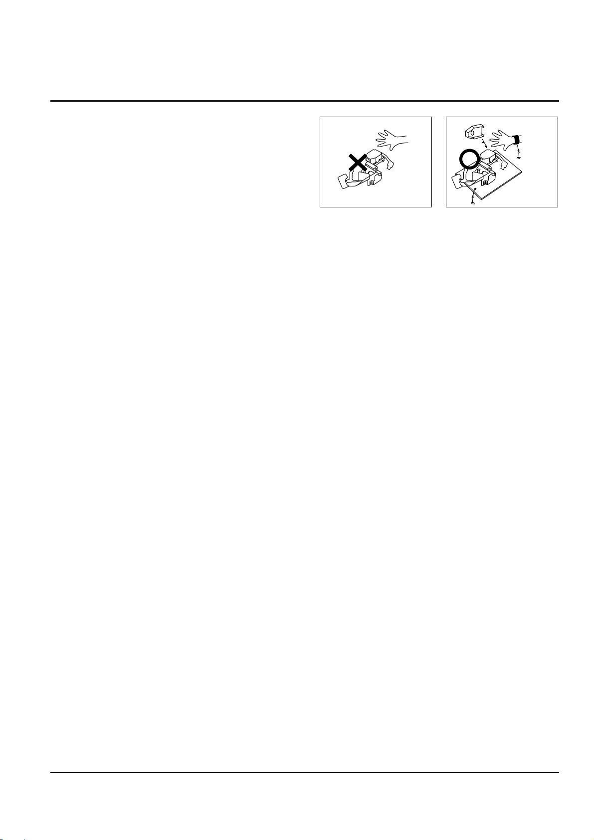
1-4 Handling the optical pick-up
The laser diode in the optical pick up may suffer electrostatic breakdown because of potential static electricity from clothing and your body.
The following method is recommended.
(1) Place a conductive sheet on the work bench (The
black sheet used for wrapping repair parts.)
(2) Place the set on the conductive sheet so that the
chassis is grounded to the sheet.
(3) Place your hands on the conductive sheet(This
gives them the same ground as the sheet.)
(4) Remove the optical pick up block
(5) Perform work on top of the conductive sheet. Be
careful not to let your clothes or any other static
sources to touch the unit.
3 Be sure to put on a wrist strap grounded to the
sheet.
3 Be sure to lay a conductive sheet made of copper etc.
Which is grounded to the table.
Fig.1-3
(6) Short the short terminal on the PCB, which is in-
side the Pick-Up ASSÕY, before replacing the PickUp. (The short terminal is shorted when the PickUp AssÕy is being lifted or moved.)
(7) After replacing the Pick-up, open the short termi-
nal on the PCB.
THE UNIT
WRIST-STRAP
FOR GROUNDING
1M
1M
CONDUCTIVE SHEET
Precautions
1-6 Samsung Electronics
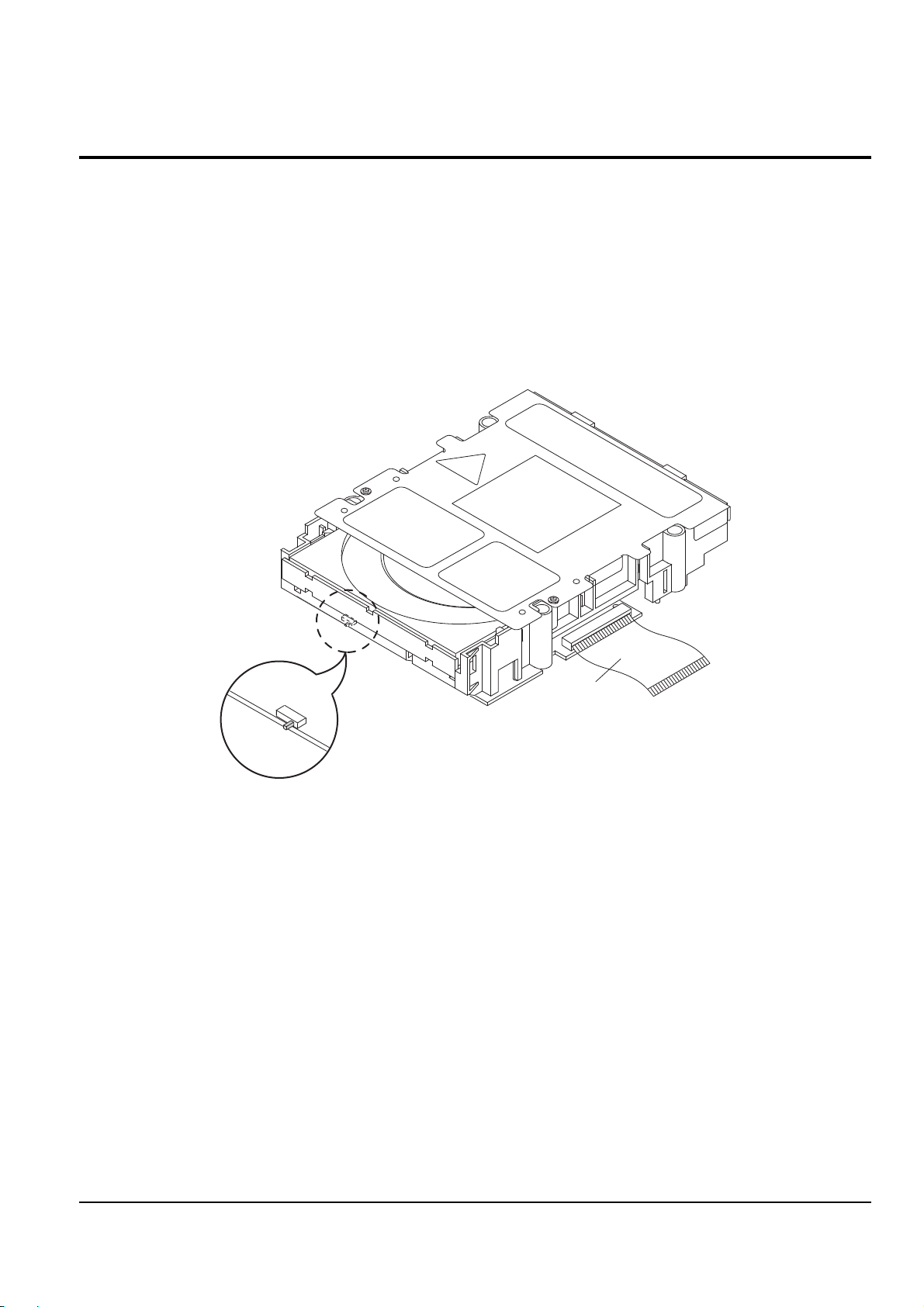
1-5 Pick-up disassembly and reassembly
1-5-1 Disassembly
1) Remove the power cable.
2) Switch LD SW3 on deck PCB to ÔOFFÕ before
removing the FPC
( Inserted into Main PCB CN6. See Fig. 1-4)
3) Disassemble the deck.
4) Disassemble the deck PCB.
1-5-2 Assembly
1) Replace the Pick-up.
2) Assemble the deck PCB.
3) Reassemble the deck.
4) Switch LD SW3 on deck PCB to ÔONÕ and insert
FPC into Main PCB CN6 (See Fig 1-4).
SW3
ON
OFF
FPC
Note : If the assembly and disassembly are not done in correct sequence, the Pick-up may be damaged.
Fig. 1-4
Samsung Electronics 2-1
2. Reference Information
2-1 IC Dsecriptions
2-1-1 AIC1 (AK4324 ; Digital-to-Analog Converter)
Serial Input
Interface
De-emphasis
Control
8X
Interpolator
8X
Interpolator
∆ ∑
Modulator
SCF
SCF
∆ ∑
Modulator
Clock Divider
DIF0 DIF1 DIF2 DEM0 DEM1 AVDD AVSS
VREFDVSSDVDDCKSMCLK
LRCK
BICK
SDATA
SMUTE
DFS
DZFL
AOUTL+
AOUTL-
AOUTR+
AOUTR-
DZFR
PD
NAME
DVSS
DVDD
CKS
MCLK
BICK
SDATA
PD
I/O
I
I
I
I
I
PIN
1
2
3
4
5
6
I
7
LRCK
I
8
FUNCTION
NAME
I/O
PIN
FUNCTION
Digital ground pin
Digital power supply
Master clock select pin (Internal pull-down pin)
Nomal speed "L":MCLK = 256fs, "H":MCLK = 384fs
Double speed "L":MCLK = 128fs, "H":MCLK = 192fs
Master clock input pin
Power-Down mode pin. When at "L", the AK4324 is in
power-down and is held in rest.
The AK4324 should always be reset upon power-pin
I SMUTE
9
I DFS
10
I DEM0
11
Soft mute pin
When this pin goes "H", soft mute cycle is initiated
When returning "L", the output mute releases.
Audio serial data input pin
64fs clock is recommended to be input on this pin
Audio serial data input pin
2's complement MSB-first data is input on this pin.
Double speed sampling mode pin (Internal pull-down pin)
"L":normal speed, "H":double speed
L/R clock pin.
De-emphasis frequency select pin
I DEM1
12
De-emphasis frequency select pin
Note : Allinput pins except internal pull-down pins should not be left floating.
-
DZFL
O
Lch positive analog output pin
Analog ground pin
Voltage reference input pin
Analog power supply pin.
Rch zero input detect pin
Lch zero input detect pin
I DIF0
13
Digital input format pin
I DIF1
14
Digital input format pin
I DIF2
15
Digital input format pin
0 AOUTR-
16
Rch negative analog output pin
O AOUTR+
17
Rch positive analog output pin
O AOUTL-
AOUTL+
18
O
19
AVSS
-
20
VREF
O
21
AVDD
O
22
DZFR
O
23
24
Lch negative analog output pin
Reference Information
2-2 Samsung Electronics
2-1-2 RIC1 (KS1461 ; RF)
100 99 98 97 96 95 94 93 92 91 90
VZOCTL
PLLGF
EQF
EQG
RDPF
AGCP
AGCB
AGCLEVEL
EQGND
AGCI
AGCC
89
RFAGCO
88
EQIN
87
BCATH
86
RFEQO
85
EQVCC
84
MIRRI
83
CP 1
81
MROFST
80
RFRPN
82
CB 1
78
CP 2
77
CB 2
76
RFCT
79
RFRP
75 BCAO
74 BCAI
73 RESET
72 OSC
71 STB
70 CLOCK
69 DATA
68 RREFDLY
67 VREFDPD
66 DPDGND
65 TE1RES
64 PLLCTL
63 DPDMUTE
62 FAUL TOUT
61 DPDEQ2
60 DPDEQ1
59 TE30FST
58 BCA
56 DPDVCC
55 DFCT2
54 DFCT1
53 DFCTTH1
52 DFCTTH2
51 DVCC
50
CC2
49
CC1
48
DFCT_CP2
47
DFCT_CP1
46
FOKB
45
FOKTH
44
DGND
43
ENV42ENVB
41
ENVP
40
ABCDI
39
ABCD
38
ABCDN
37
PDLIMITRES
36TE35
TEN
34
FEN
33
FE
32
AGND
31
PDCD
30
LDOCD
29
PDVD
28
LDODVD
27
VREFLP_BGI
26
OFSTHOLD
25
FOFST
24
VREFA
23
AVCC
22
DCD1
21
CCD1
20
BCD1
19
ACD1
18
DDVD1
17
CDVD1
16
BDVD1
15
ADVD1
14
F
13
E
12
VREFEQ
11
RREF
10
RREFEQ
9
RREFBF
8
DDVD
7
CDVD
6
BDVD
5
ADVD
4
DCD
3
CCD
2
BCD
1
ACD
to RF EQ
TUNING BLOCK
AGC-HOLD(OOH)
MUX
AGC_DET
RF
MUX
VREF
GENERATOR
CDRSEL(00H)
EQ
VC AMP
D
D
D
D
MUX3
GAIN_TE3(02H)
GCA
OFSTHOLD
TEOFST(04H)
TBAL(01H)
TE38
SUB
RF
MUX
D1
B1
C1
A1
FE
GAIN_FE(03H)
FE_0FST(05H)
CDRSEL(00H)
ANALOG
VC AMP
ALPC
LDONB(00H)
FOFST
OFSTHOLD
MUX
TESEL(OOH)
OFSTHOLD
ABCD_OFST(O6H)
ENVELOPE FOK DEFECT
MUX
ENV_SEL(02H)
EQIN
CDRSEL(OOH)
ABCD
SUM
GAIN_ABCD(OOH)
DELAY_SEL(00H)
PLLCTL
FAULTOUT
PDLIMITRES
TEOPST(04H)
PD,LPFDELAY
TE1_LIMIT
DELAY_SEL(OOH)
PLLCTL
TBAL(O1H)
HOLD_CTL(O8H)
DPDMUTE
DPD_MUTE(O2H)
SEOFHOLD
FLT_CTL(OOH)
CAL_ENDB(O2H)
COM
COM
DPDEQ2
DPDEQ1
GCA
GCA
EQ
EQ
CD1
S12
DVD1
DVD2
LDONB
FLT_CTL
CDRSEL
TESEL
AGC-HOLD
TBAL
GAIN_TE3
ENV_SEL
DVCTL_SEL
DPD_MUTE
GAIN_EQ
GAIN_FE
GAIN_ABCD
TE_OFST
FE_OFST
ABCD_OFST
DELAY_CD
DELAY_AB
PDLIMIT
ga_RFSUM
HOLD_CTL
ga_PLLDP
ga_PLLDN
to DPD
BLOCK
DPD
BLOCK
S/IF
BLOCK
AUTO
OFSTCTL
BCA
BLOCK
BCA
RFCT
&
MIRR
RFRP
TE1RES
CD1 S12 DVD1.2
RF
Equalizer
RF SLM
& AGC
A
B
C
D
GAIN_EQ(02H)
MIRR57
Reference Information
Samsung Electronics 2-3
17
16
15
14
13
12
11
10
9
8
7
6
5
4
3
2
CD optical main beam A AC coupling input port for RF
CD optical main beam B AC coupling input port for RF
CD optical main beam C AC coupling input port for RF
CD optical main beam D AC coupling input port for RF
DVD optical main beam A AC coupling input port for RF
DVD optical main beam B AC coupling input port for RF
DVD optical main beam C AC coupling input port for RF
DVD optical main beam D AC coupling input port for RF
RF AMP I/O buffer bias resistance connection port
RF EQ bias resistance connection port
Analog block bias resistance connection port
CAP connection port for RF EQ center voltage
CD optical sub beam E input port for SERVO
CD optical sub beam F input port for SERVO
DVD optical main beam A input port for SERVO
DVD optical main beam B input port for SERVO
DVD optical main beam C input port for SERVO
1 ACD
BCD
CCD
DCD
ADVD
BDVD
CDVD
DDVD
RREFBF
RREFEQ
RREF
VREFEQ
E
F
ADVD1
BDVD1
CDVD1
FUNCTIONPIN NAME I/O
I
I
I
I
I
I
I
I
-
-
O
I
I
I
I
I
-
38
37
36
35
34 FE Input port for AMP GAIN setting
Input port for TE AMP GAIN setting
TE AMP output port
Bias resistance port for PDLIMIT
Input port for ABCD AMP GAIN setting
FEN
TEN
TE
PDLIMTRES
ABCDN
FUNCTIONPIN NAME I/O
I
I
O
-
I
28
27
26
25
24
23
22
21
20
19
DVD optical main beam D input port for SERVO
CD optical main beam F input port for SERVO
CD optical main beam F input port for SERVO
CD optical main beam F input port for SERVO
CD optical main beam F input port for SERVO
Power voltage input port for analog part
CAP connection port for analog part
center voltage, Use at other block
CAP connection port for focus auto offset (OPEN)
ON/OFF connection port for auto offset block (L :
auto offset adjustment H : serial offset adjustment)
BANDGAP voltage input port for ALPC
DVD optical laser diode driving voltage output port
18 DDVD1
ACD1
BCD1
CCD1
DCD1
AVCC
VREFA
FOFST
OFSTHOLD
VREFLP_BGI
LDODVD
I
I
I
I
I
-/O
O
IOI
P
32
31
30
29 DVD optical laser monitor diode voltage input port
CD optical laser diode driving voltage output port
CD optical laser monitor diode voltage input port
Power GND port for analog part
PDDVD
LDOCD
PDCD
AGND
I
O
I
P
33 FE AMP output portFE
O
ABCD AC coupling input port for SERVO monitorABCDI I
48
47
46
45
44
43
42
41
40
ABCD AMP output port
Peak hold time constant setting RC
connection port for RF envelope detect
Bottom hold time constant setting RC
connection port for RF envelope detect
RF envelope detect output port
Power GND input port for digital circuit
Focus OK comparing level input port
Focus OK comparator output port
(L: FOCUS OK)
Peak hold time constant connection port SERVO
defect max. time setting
Peak hold time constant connection port PLL defect
min. time setting
39 ABCD
ENVP
ENVB
ENV
DGND
FOKTH
FOKB
DFCT_CP1
DFCT_CP2
O
-
-
O
I
O
-
-
P
62
61
60
59
58
57
56
55
54
53
52
51
50
49 Output port of peak detector for defect
AC coupling input port for defect
Power voltage input port for digital circuit
Resistance connection port for PLL defect comparat-
ing level setting
Resistance connection port for SERVO defect com-
parating level setting
Defect output port for SERVO
Defect output port for PLL
Power voltage input port for DPD TE
Mirror output port
BCA output port
Resistance connection port for 3BTE offset
DPD EQ (A+C) output port
DPD EQ (B+D) output port
DPD defect waveform output port (MONITOR)
CC1
CC2
DVCC
DVCTTH2
DFCTTH1
DFCT1
DFCT2
DPDVCC
MIRR
BCA
TE3OFST
DPDEQ1
DPDEQ2
FAULTOUT
O
P
-
-
I
O
O
P
O
O
-
O
O
O
64
DPD TE MUTE control port (H : MUTE)
DPD TE PLL variable input port
63 DPDMUTE
PLLCTL
I
I
FUNCTIONPIN NAME I/O FUNCTIONPIN NAME I/O
87
86
85
84
83
82
81
80
79
78
77
76
75
74
73
72
71
70
69
68
67
66
65 DPD TE PLL variable bias resistance
Power GND input port for DPD TE
CAP connection port for DPD TE center
Bias resistance connection port for delta block
Data input port
Clock input port
Data enable input port
OSC time constant input port for auto offset block
Reset input port for auto offset block (L : RESET)
BCA FILTER1
BCA FILTER2
RF ripple center voltage output port for mirror
Bottom hold time constant RC connection port for
RFCT generation
Peak hold time constant RC connection port for
RFCT generation
RF ripple AMP output port for mirror
RF ripple AMP GAIN input port for mirror
RF ripple offset control port for mirror
Bottom hold time constant RC connection port for
RFCT generation
Peak hold time constant RC connection port for
RFCT generation
Input port for MIRR signal generation
Power voltage input port for RF EQ
RF EQ output port
BCA comparating level control port
TE1RES
DPDGND
VREFDPD
RREFDLY
DATA
CLOCK
STB
OSC
RESET
BCAI
BCAO
RFCT
CB2
CP2
RFRP
RFRPN
MROFST
CB1
CP1
MIRRI
EQVCC
RFEQO
BCATH
I
P
O
-
I
I
I
I
I
O
O
-
-
O
I
I
-
-
I
P
O
I
91
90
89
RFAGCO input port for RF EQ
RF AGC AMP output port
AGC time constant CAP connection port
When AGC is “HOLD”, AGC voltage input port
88 EQIN
RFAGCO
AGCC
AGCI
I
O
-
I
95
94
93
92 Power GND input port for RF EQ
AGC level control voltage input port
RF bottom hold time constant RC connection port for RF AGC
RF peak hold time constant RC connection port for RF AGC
EQGND
AGCLEVEL
AGCB
AGCP
P
I
-
-
100
99
98
97
96
Bias resistance connection port for RF EQ frequency setting
RF EQ boost gain control voltage input port
RF EQ peak frequency control voltage input port
RF EQ boost, peak frequency gain control port corre-
sponding to wideband PLL (PLLG. PLLF resistance
internal design)
RF EQ control port (When No. PLLG isn’t adjusted,
apply DC CTL voltage.)
RDPF
EQG
EQF
PLLGF
VZOCTL
-
I
I
I
I
Reference Information
2-4 Samsung Electronics
2-1-3 SIC1 (KS1452 ; Digital Servo)
A/D
CONVERTER
BLOCK
D/A
CONVERTER
BLOCK
TRACK
COUNTER
EFM
ASYMETRY
VREF
ENV
TZCO
SME
TE
FE
COUT
FOD
TRD
SLD
SPD
FBAL
TBAL
DVCTL
EFMI
RFI
ASYDVD
ASYCD
EFM
EFMOA
PLLHD
INTO_224
FDCTL
MAGICO
EQCTL
VCTRL
RVCO
PLCK
EFMRTD
RPD
RFD
PLLLOCK
MDOUT[3:0]
PSB
SENSE
MDATA[7:0]
MRDB
MWRB
CSB
DAB
SCOR
SQSI
SQCK
LDONB
TLKB
FLKB
DIRC
PS1
SSTOP
/PSO
SMON
LOCK
DFCT
FOKB
MIRR
TZCA
PHI1
XOUT
XO
XI
TEST
RSTB
TILTO
TILTI
ROM
DSP CORE
FOR
DIGITAL SERVO
TIMING
GENERATOR
I/O INTERFACE
BLOCK
SUB CODE
READ BLOCK
SYSCON
INTERFACE
BLOCK
WIDE
CAPTURE
RANGE PLL
Reference Information
Samsung Electronics 2-5
33
32
31
30
29
28
27
26
25
24
23
22
21
20
19
18
17
16
15
14
13
12
11
10
9
8
7
6
5
4
3
2
Mode data3 out controlled by micom
Limit switch/sled position sensor input pin0
Sled motor position sensor input pin 1
Test pin (L : normal H : test)
Counter clock
Focus servo lock signal output pin
Tracking servo lock signal output pin
0 : 1BIT 1 : 8BIT
System reset signal input pin
Micom chip select pin
Micom data/address select pin
Micom write clock signal input pin
Micom read clock signal input pin
Micom data pin 0
Micom data pin 1
Micom data pin 2
Micom data pin 3
Micom data pin 4
Micom data pin 5
Micom data pin 6
Micom data pin 7
Internal status monitor pin
Servo logic & ROM VDD power supply pin
System clock signal input pin
System clock signal output pin
Clock out (33.9688MHz) to DSP
Servo logic & ROM VSS power supply pin
Clock output pin for subcode data read
Subcode data input pin
Timing detection input pin for subcode data read
Motor ON signal input pin
Lock signal input pin
Direct jump control (for 1 track jump)
1 MDOUT3
SSTOP/PSO
PS1
TEST
COUT
FLKB
TLKB
PSB
RSTB
CSB
DAB
MWRB
MRDB
MDATA0
MDATA1
MDATA2
MDATA3
MDATA4
MDATA5
MDATA6
MDATA7
SENSE
DVDD
XI
XO
XOUT
DVSS
SQCK
SQSI
SCOR
SMON
LOCK
DIRC
FUNCTIONPIN NAME I/O
O
I
I
I
O
O
O
I
I
I
I
I
I
I/O
I/O
I/O
I/O
I/O
I/O
I/O
I/O
O
P
I
O
O
P
O
I
I
I
I
I
64
63
62
61
60
59
58
57
56
55
54
53
52
51
50
49
48
47
46
45
44
43
42
41
40
39
38
37
36
35
Focus OK signal input pin
PLL frequency detect control input pin
Laser diode ON signal output pin
Defect Detection signal input pin
Mirror signal input pin
PLL hold signal from micom
Servo interrupt monitor pin
PLL logic block VDD power supply pin
PLCK
Frequency lock detect output
(H : Lock L : Unlock)
Latched EFM output signal
PLL logic block VSS power supply pin
Resistor pin for VCO GAIN
Gain adjust resister for frequence detector
Gain adjust resister for phase detector
Control voltage for VCO
Input for hysteresis control of FD output (for test)
EFM offset adjustment pin
Tracking zero cross output pin
Servo CPU VDD power supply pin
EQ control signal
EFM signal for test
EFM signal
Asymmetric input signal for DVD
Asymmetric input signal for CD
RF input signal
Servo CPU VSS power supply pin
Analog block VSS power supply pin
Spindle error input pin
Reference voltage input pin
Tracking error signal input pin
34 FOKB
FDCTL
LDONB
DFCT
MIRR
PLLHD
INTO_224
PVDD
PLCK
PLLLOCK
EFMRTD
PVSS
RVCO
RFD
RPD
VCTL
MAGICO
EFMOA
TZCO
SVDD
EQCTL
EFMI
EFMO
LPFDVD
LPFCD
RFI
SVSS
AVSS
SME
VREF
TE
FUNCTIONPIN NAME I/O
I
I
O
I
I
I
O
P
O
O
O
P
I
I
I
I
I
I
O
P
O
I
O
I
I
I
P
P
I
I
I
72
71
70
69
68
67
66
Focus error signal input pin
RF envelope input pin
Tilt in (reserved)
Analog block VDD power supply pin
Tilt out (reserved)
Depth variation control signal output pin
Tracking balance signal output pin
Focus balance signal output pin
65 FE
ENV
TILTI
AVDD
TILTO
DVCTL
TBAL
FBAL
FUNCTIONPIN NAME I/O
I
I
I
P
O
O
O
O
80
79
78
77
76
75
74
73 Sled motor drive signal output pin
Spindle motor drive signal output pin
Focus actuator drive signal output pin
Tracking actuator drive signal output pin
TE signal for tracking zero cross input pin
Mode data 0 out controlled by micom
Mode data 1 out controlled by micom
Mode data 2 out controlled by micom
SLD
SPD
FOD
TRD
TZCA
MDOUT0
MDOUT1
MDOUT2
FUNCTIONPIN NAME I/O
O
O
O
O
I
O
O
O
Reference Information
2-6 Samsung Electronics
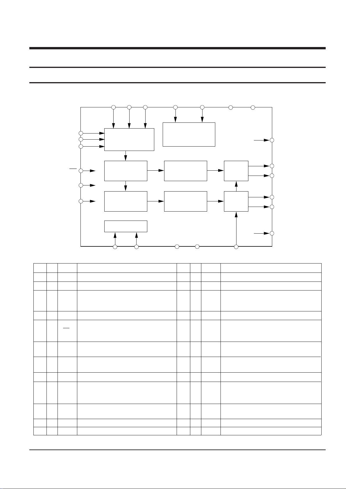
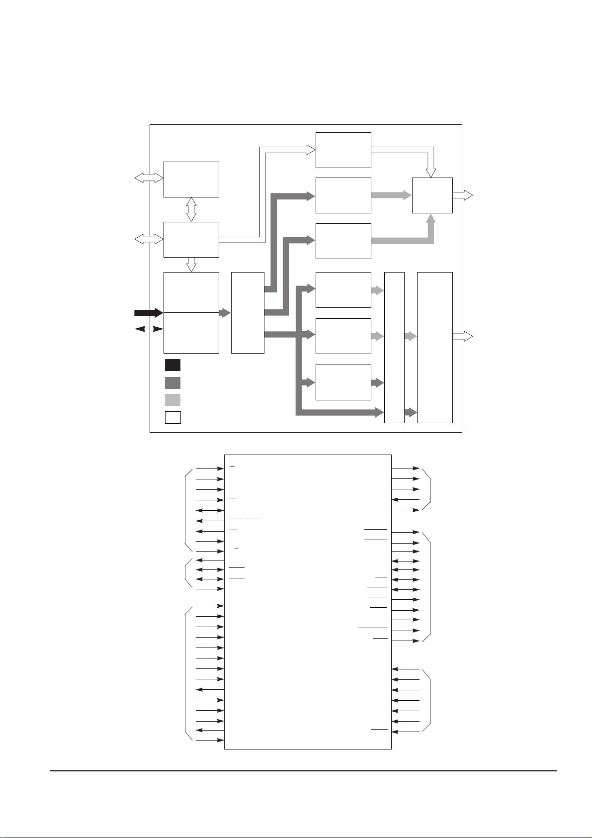
2-1-4 DIC1 (KS1453 ; DVD Data Processor)
X'TAL &
TIMING GEN
RFCK 17.58/7.35KHz
DVD CLV/CAV
CD CLV/CAV
M
23BIT SR
26.16MHz
32BIT SR 16-8 DEMOD
ECSY
FRAME SYNC
DET/PROT/INS
(17.57KHz)
(6, 4, 3)
efmwr ID ECC
WFCK 17.58/7.35KHz
M
VCO TIMING
GENERATOR
17.58KHz = 26.16M/1488
676.08Hz
(208, 192, 17)
(182, 172, 11)
ECC
VCO TIMING
GENERATOR
7.35KHz = 4.3218M/588
75Hz
(32, 28, 5)
(28, 24, 5)
CIRC
FRAME SYNC
DET/PROT/INS
(7.35KHz)
EFM DEMOD
SUBCODE I/F
CD-G
V-CD, CD-DA
SQ-VCD
DVDP,
DEINTERLEAVE
&
RAM CONTROL
(6, 4, 3)
trans ID ECC
EDC
DESCRAMBLER
MICOM I/F
M M
TO MICOM (15)
MDAT(7:0), MRZA, ZCS, MWR,
MRD, ZIRQZD, ZWAIT, ZRST
TO DRAM
256K*16
(32)
DD(15:0)
DADR(8:0)
ZRAS
ZUCAS
ZLCAS
ZOE(1:0)
ZWE(1:0)
TO AV (13)
SDATA[0] / CDATA
SDATA[1] / LRCK
SDATA[2] / BCLK
SDATA[3] / C2PO
SDATA[4] / SQDT
SDATA[5] / WFSY
SDATA[6] / SOS1
SDATA[7] / SQCK
DATREQ
CSTROBE
DTER
DATACK
TOS
TO (12)
XTI1
XTO1
CK33MI
CK33MO
FG
MON
MDP
MDS
FSW
PLL_LOCK
CLV_LOCK
SERVO_LOCK
FROM R/F,
PLL(3)
EFMI
PLCK
BCARZ
TO D-EQ (8)
PWMO(7:0)
Monitor(8) GFS, FRSYZ, TX, EFMO, WFCK, RFCK, CK 16M, DEMPHA Power(34)=VDD(11)+GND(23) Test Pin(3) TEST0, TEST1, TEST2
Reference Information
Samsung Electronics 2-7
DRAM data bus32 DD9_BI
Digital GND (0V)31 DVSS
DRAM data bus30 DD5_BI
DRAM data bus29 DD10_BI
DRAM data bus28 DD4_BI
DRAM data bus27 DD11_BI
Digital power (+5V)26 DVDD
DRAM data bus25 DD3_BI
DRAM data bus24 DD12_BI
DRAM data bus23 DD2_BI
DRAM data bus22 DD13_BI
Digital GND (0V)21 DVSS
DRAM data bus20 DD1_BI
DRAM data bus19 DD14_BI
DRAM data bus18 DD0_BI
DRAM data bus17 DD15_BI
Digital GND (0V)16 DVSS
System clock output for 26.16 MHz15 XTO_OUT
System clock input for 26.16 MHz14 XTI_IN
Digital power (+5V)13 DVDD
Micom data bus12 MDAT0_BI
Micom data bus11 MDAT1_BI
Micom data bus10 MDAT2_BI
Micom data bus9 MDAT3_BI
Micom data bus8 MDAT4_BI
Micom data bus7 MDAT5_BI
Micom data bus6 MDAT6_BI
Micom data bus5 MDAT7_BI
Digital GND (0V)4 DVSS
Micom register select
(L -> Register H -> Data)
3
MRZA_IN
Chip select (Active Low)2 ZCS_IN
Digital GND (0V)1 DVSS
FUNCTIONPIN NAME
DVD data/Sub code frame sink (WFSY)65 SDATA5_OUT
DVD data/Sub code serial data (SQDT)64 SDATA4_OUT
DVD data/CD data error flag (C2P0)63 SDATA3_OUT
DVD data/CD data bit clock (BLCK)62 SDATA2_OUT
DVD data/CD data L/R clock (LRCK)61 SDATA1_OUT
DVD data/CD data bitstream output60 SDATA0_OUT
Digital power (+5V)59 DVDD
Data acknowledge signal output58 DATACK_OUT
Top of sector57 TOS_OUT
Digital GND (0V)56 DVSS
Digital GND (0V)55 DVSS
DRAM address bus54 DADR3_OUT
DRAM address bus53 DADR4_OUT
DRAM address bus52 DADR2_OUT
DRAM address bus51 DADR5_OUT
DRAM address bus50 DADR1_OUT
DRAM address bus49 DADR6_OUT
DRAM address bus48 DADR0_OUT
Digital GND (0V)47 DVSS
DRAM address bus46 DADR7_OUT
DRAM address bus45 DADR8_OUT
DRAM row address strobe44 ZRAS_OUT
DRAM output enable 043 ZOEO_OUT
Digital power (+5V)42 DVDD
DRAM output enable 1 (16M, --------, 16M)41 ZOE1_OUT
DRAM write enable 0 (4M, 8M, 16M)40 ZWE0_OUT
DRAM write enable 1 (8M ONLY)39 ZWE1_OUT
DRAM upper column address strobe38 ZUCAS_OUT
DRAM row column address strobe37 ZLCAS_OUT
Digital GND (0V)36 DVSS
DRAM data bus35 DD7_BI
DRAM data bus34 DD8_BI
DRAM data bus33 DD6_BI
FUNCTIONPIN NAME
Digital GND (+5V)97 DVSS
System clock output for 33.8688MHz96 CK33MO_OUT
System clock input for 33.8688MHz95 CK33MI_IN
Digital out92 TX_OUT
Good frame sync detection result output (“H”
active)
93 GFS_OUT
Frame sync out91 FRSYZ_OUT
Digital GND (0V)90 DVSS
Digital GND (0V)89 DVSS
Digital GND (0V)88 DVSS
Digital GND (0V)87 DVSS
Digital power (+5V)86 DVDD
Digital power (+5V)85 DVDD
Digital GND (0V)84 DVSS
Digital GND (0V)83 DVSS
Digital GND (0V)82 DVSS
PWM output signal81 PWM00_OUT
PWM output signal80 PWM01_OUT
PWM output signal79 PWM02_OUT
PWM output signal78 PWM03_OUT
Digital power (+5V)77 DVDD
PWM output signal76 PWM04_OUT
PWM output signal75 PWM05_OUT
PWM output signal74 PWM06_OUT
PWM output signal73 PWM07_OUT
Digital GND (0V)72 DVSS
DVD data error output71 DTER_OUT
Data request from A/V decoder or ROM decoder70 DATREQ_IN
Data strobe (clock) output69
CSTROBE_OUT
Digital GND (0V)68 DVSS
DVD data/Sub code serial clock (SQCK)67 SDATA7_BI
DVD data/Sub code block sink (S0S1)66 SDATA6_OUT
FUNCTIONPIN NAME
Micom write strobe (schmidt trigger)128 MWR_IN
Micom read strobe (schmidt trigger)127 MRD_IN
Interrupt request from micom126 ZIRQZD_OUT
Micom read/write access wait (“L” wait)125 ZWAIT_OUT
Hardware reset active low124 ZRST_IN
Digital GND (0V)123 DVSS
BCA input signal122 BCARZ_IN
When DEEMPHASIS is ON, “HIGH”.121 DEMPHA_OUT
2∫–¡÷ clock of CK33M/16.934MHz120 CK16M_OUT
Digital power (+5V)119 DVDD
Digital power (+5V)118 DVDD
Spindle motor output filter conversion output (3-
state)
115
FSW_OUT
Digital power (+5V)117 DVDD
EFM/EFM+ signal input116 EFMI_IN
Reference signal for CAV114 FG_IN
Spindle motor ON/OFF control output113 MON_OUT
Spindle motor speed control signal
(3-state)
110 MDS_OUT
Spindle motor phase control signal
(3-state)
109 MDP_OUT
Digital GND (0V)112 DVSS
Digital GND (0V)111 DVSS
Lock signal for SERVO108 SERLOCK_OUT
Lock signal for CLV107 CLVLOCK_OUT
Lock signal for PLL106 PLLLOCK_OUT
Digital GND (0V)105 DVSS
Phase locked clock104 PLCK_IN
Reference frame pulse103 RFCK_OUT
Write frame pulse102 WFCK_OUT
EFM out101 EFMO_OUT
Test mode setting port100 TEST2_IN
Test mode setting port99 TEST1_IN
Test mode setting port98 TEST0_IN
FUNCTIONPIN NAME
Digital GND (0V)94 DVSS
Reference Information
2-8 Samsung Electronics
2-1-5 DIC2 (KM416C254BJ-6 ; CMOS DRAM)
NAME
A0-A8
DQ0-15
VSS
RAS
UCAS
LCAS
W
OE
V
CC
N.C
BLOCK DIAGRAM
Control
Clocks
VBB Generator
Lower
Data in
Buffer
DQ0
to
DQ7
OE
DQ8
to
DQ15
Lower
Data out
Buffer
Upper
Data in
Buffer
Upper
Data out
Buffer
Vcc
Vss
RAS
UCAS
LCAS
W
FUNCTION
Address Inputs
Data in/Out
Ground
Row Address Strobe
Upper Column Address Strobe
Lower Column Address Strobe
Read/Write Input
Data Output Enable
Power (+5V)
Power (+3.3V)
No Connection
Refresh Timer
Refresh Control
AO
.
.
A8
Refresh Counter
Row Address Buffer
Col. Address Buffer
Row Decoder
Column Decoder
Memory Array
262,144 x 16
Cells
Reference Information
Samsung Electronics 2-9
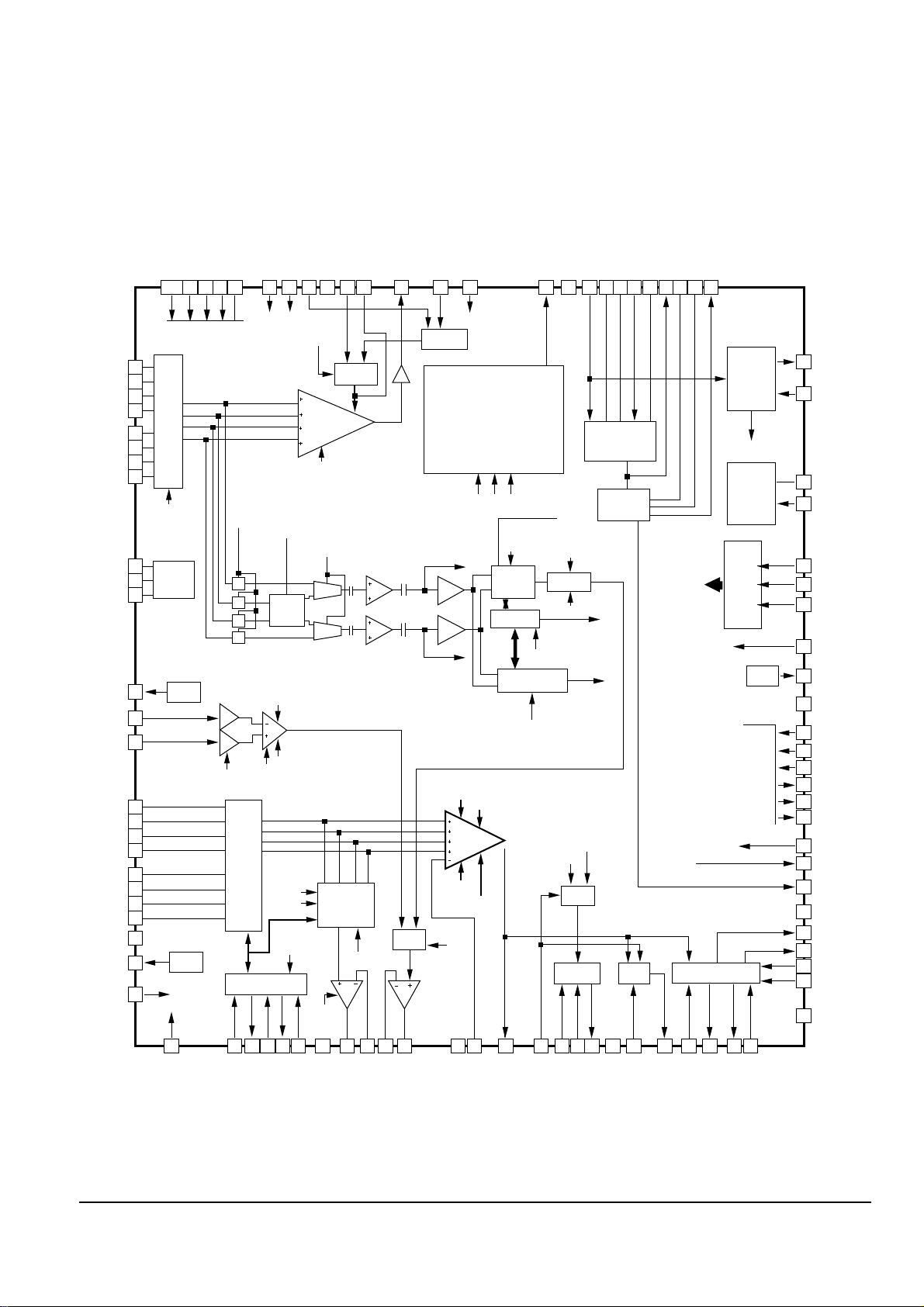
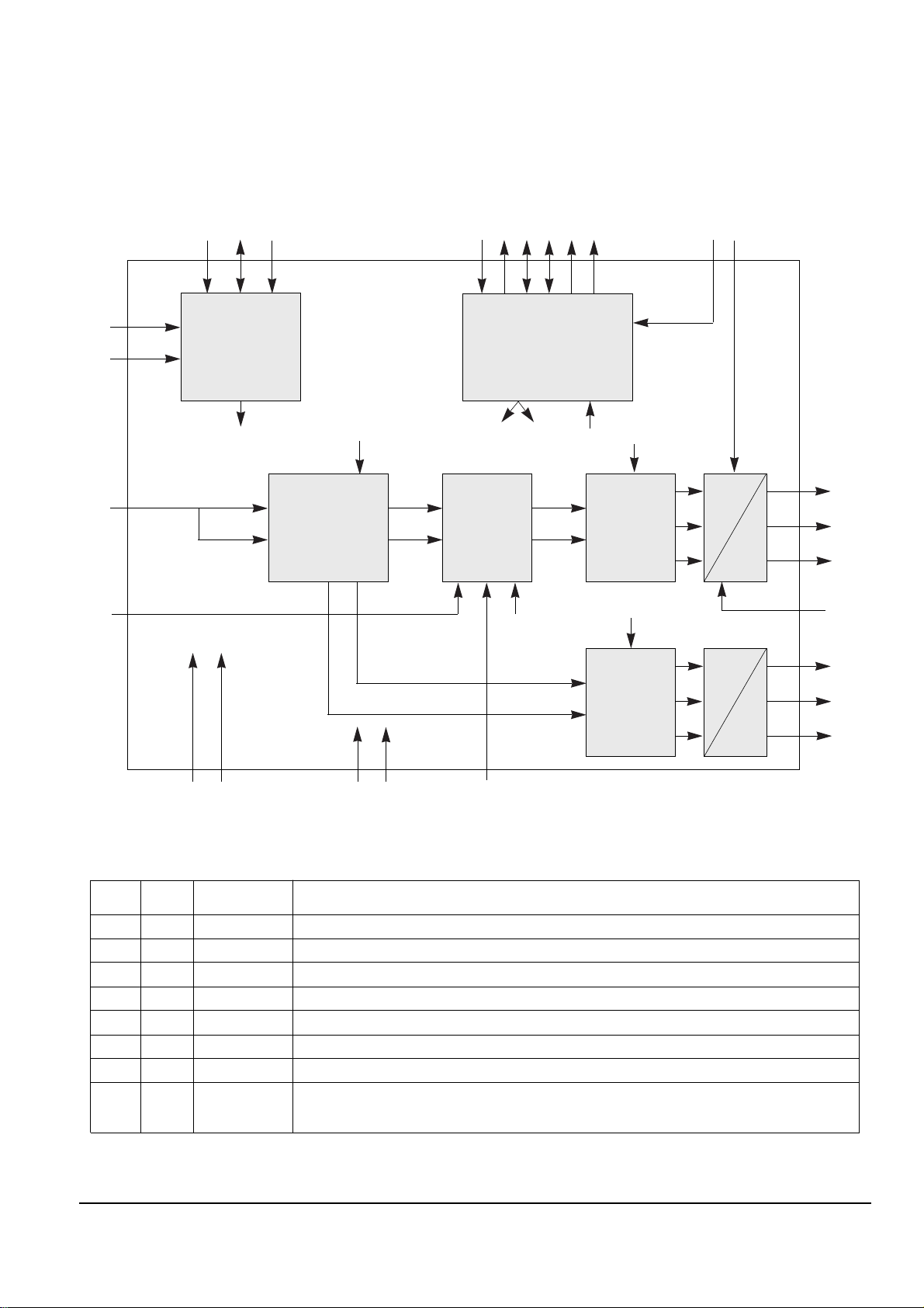
2-1-6 VIC1 (ZiVA-3 ; Audio/Video Decoder)
Memory
Controller
OSD
Decoder
Video
Interface
Audio
Interface
Subpicture
Decoder
MPEG
Video
Decoder
CD-DA and
LPCM
Decoder
Dolby Digital
Audio
Decoder
MPEG
Audio
Decoder
Host
Interface
Control Logic
Secure View
CSS
Descrambling
Bus Key
Authentication
(Optional)
SDRAM/
EDO/ROM
Interface
Host
Interface
DVD/CD
Interface
BLOCK DIAGRAM
Video
Mixer
ZiVA-3 Decoder
Stream
Program
Decoder
Audio
DSP
Audio
Interface
Digital
Scrambled, Compressed Content
Descrambled, Compressed Content
Decompressed Content
Display Content
LOGIC DIAGRAM
HADDR[2:0]
RD
HDATA[7:0]
WAIT/DTACK
INT
HOST8SEL
Host
Interface
Signals
Video
Interface
Signals
DVD/CD
Interface
Signals
Audio
Interface
Signals
SDRAM/EDO
Interface
Signals
Global
Interface
Signals
DA-DATA[0:3]
DA-LRCK
DA-BCK
DA-XCK
DA-IEC
EDO-CAS
EDO-RAS
LDQM
MDATA[15:0]
MADDR[20:0]
MWE
ROM-CS
SD-CLK
SD-CAS[1:0]
UDQM
SYSCLK
VDD
VSS
A_VSS
A_VDD
P10[10:0]
RESET
VDATA[7:0]
VCLK
DVD-DATA0/CD-DATA
DVD-DATA1/CD-LRCK
DVD-DATA2/CD-BCK
DVD-DATA3/CD-C2PO
DVD-DATA4/CDG-SDATA
DVD-DATA5/CDG-VFSY
DVD-DATA6/CDG-SOS1
DVD-DATA7/CDG-SCLK
VREQUEST
VSTROBE
ERROR
V-DACK/ASTROBE
AREQUEST
A-DACK
DTACKSEL
CS
R/W
VSYNC
HSYNC
SD-CAS
SD-RAS
ZiVA Decoder
Reference Information
2-10 Samsung Electronics
2-1-7 VIC50 (SAA7128 ; Digital Video Encoder)
I2C-
INTERFACE
SYNC/
CLOCK
MP
MP
9..16
44
20
21
I
2
C-Control
I
2
C-Control
I
2
C-Control
I
2
C-Control
I
2
C-Control
Clock&Timing
RESN
40
42
41
35
34
7
8
43
37
4
25,28,31,36
SDA
SCL
XTALI
XTAL
RCV1
RCV2
TTXRQ
XCLK
LLC1
VDDA
VDD I2C
SA
MP(7:0)
TTX
FADER
ENCODER
OUTPUT-
INTERFACE
D
A
RGB-
PROCESSOR
D
22,32,33
23
26
29
30
27
Y
C
Y
5,18,38
6,17,39
2
3
VSS
VDD
SP
AP
19
RTC1
CbCr
Y
CbCr
24
R(Cr)
VSSA
G(Y)
B(Cb)
CVBS
(CSYNC)
VBS
(CVBS)
C
(CVBS)
A
BLOCK DIAGRAM
NAME
res.
SP
AP
LLC1
V
SS1
V DD1
RCV1
RCV2
I/O
I
I
I
I
I
I/O
I/O
PIN
1
2
3
4
5
6
7
8
FUNCTION
Reserved pin, do not connect
Test Pin;connected to digital ground for normal operation
Test Pin;connected to digital ground for normal operation
Line-Locked Clock input;this is the 27 MHz master clock
Digital supply ground 1
Digital supply 1
Raster Contral 1 for video port. This pin receives/provides a VS/FS/FSEQ signal.
Raster Contral 2 for video port. This pin provides an HS pulse of programmable length or receives
an HS pulse.
Reference Information
Samsung Electronics 2-11
NAME
MP7
MP6
MP5
MP4
MP3
MP2
MP1
MP0
V
DD2
V SS2
RTCI
VDD
12C
SA
V
SSA1
R(Cr)
C
V
DDA1
G(Y)
VBS
V
DDA2
B(Cb)
CVBS
V
DDA3
V SSA2
V SSA3
XTAL
XTAL1
I/O
I
I
I
I
I
I
I
I
I
I
I
I
I
I
O
O
I
O
O
I
O
O
I
I
I
O
I
PIN
9
10
11
12
13
14
15
16
17
18
19
20
21
22
23
24
25
26
27
28
29
30
31
32
33
34
35
FUNCTION
Digital supply voltage 2
Digital ground 2
Real Time Control input. If the LLC1 clock is provided by an SAA7111 or SAA7151B, RTCI should be
connected to the RTCO pin of the respective decoder to improve the signal quality.
Sense input for 12C bus voltage;connect to 12C bus supply
Select 12C address; low selects slave address 88h, high selects slave address 8Ch.
Analog ground 1 for Red (Cr), C(CVBS), Green(Y) outputs
Analog ground 3 for the DAC reference ladder and the oscillator
Crystal oscillator output
Crystal oscillator input; if the oscillator is not used, this pin should be connected to ground.
Analog output of Red (Cr)signal
Analog output of Chrominance (CVBS) signal
Analog supply voltage 1 for R(Cr), C(CVBS) outputs
Analog output of Green(Y) signal
Analog output of VBS (CVBS) signal
Analog supply voltage 2 for VBS(CVBS), Green(Y) outputs
Analog output of Blue(Cb) signal
Analog output of CVBS(CSYNC) signal
Analog supply voltage 3 for Blue(Cb)and CVBS(CSYNC), outputs
Analog ground 2 for VBS (CVBS), Blue(Cb), CVBS(CSYNC)outputs
Double speed 54 MHzMPEG port. It is an input for "
CCIR 656"
style multiplexed Cb, Y, Cr data.
Data are sampled on the rising and falling clock edge;data sampled on the risting edge then are sent to
the encoding part of the device, data sampled on the falling edge are sent to the RGB part of the device.
(or vice verse, depending on programming)
V DDA4
XCLK
V
SS3
V DD3
RESN
SCL
SDA
TTXRQ
TTX
I
O
I
I
I
I
I/O
O
I
36
37
38
39
40
41
42
43
44
Analog supply voltage 4 for the DAC reference ladder and the oscillator
Clock output of the crystal oscillator
Digital supply ground 3
Digital supply 3
12C serial clock input
12C serial data input/output
Teletext Request output, indicating when text bits are requested
Teletext bit stream input
Reset input, active LOW. After reset is applied, all digital I/Os are in input mode; PALBlackburst on CVBS, VBS and C;RGB outputs set to lowest voltage.
The 12C-bus receiver waits for the START condition.
Reference Information
2-12 Samsung Electronics
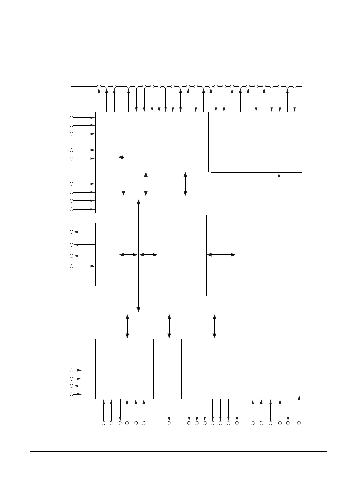
2-1-8 MIC1 (TMP93CM41F ; Main Micom)
PAO~PA6
PA7(SCOUT)
P50 to P57
(ANO to AN7)
AVCC
AVSS
VREFH
VREFL
(TXD0)P90
(RXD0)P91
(SCLK0/CTS0)P92
(TXD1)P93
(RXD1)P94
(SCLK1)P95
(PG 00)P60
(PG 01)P61
(PG 02)P62
(PG 03)P63
(PG 10)P64
(PG 11)P65
(PG 12)P66
(PG 13)P67
(T10)P70
(T01)P71
(T02)P72
(T03)P73
(INT4/T14)P80
(INT5/T15)P81
(T04)P82
(T05)P83
(INT6/T16)P84
(INT7/T17)P85
(T06)P86
(INTO)P87
VCC[3]
VSS[3]
X1
X2
CLK
XT1
XT2
AM8/16
EA
RESET
ALE
TEST2,1
NMI
WDTOUT
P00 to P07
(AD0 to AC7)
P10 to P17
(AD8 to AD15/A8 toA15
P20 to P27
(A0 to A7/A16 to A23)
P30(RD)
P31(WR)
P32(HWR)
P33(WAIT)
P34(BUSRQ)
P35(BUSAK)
P36(R/W)
P37(RAS)
P40(CS0/CAS0)
P41(CS1/CAS1)
P42(CX2/CAS2)
PORT A
High
Frequency
OSC
Low
Frequency
OSC
INTERRUPT
CONTROLLER
WATCH-DOG
TIMER
PORT 0
PORT 2
PORT 3
CS/WAIT
CONTROLLER
(3-BLOCK)
PORT 1
10-BIT 8CH
A/D
CONVERTER
SERIAL I/O
(CH,0)
SERIAL I/O
(CH,1)
PATTERN
GENERATOR
(CH,0)
PATTERN
GENERATOR
(CH,1)
16BIT TIMER
(TIMER 4)
16BIT TIMER
(TIMER 5)
8BIT TIMER
(TIMER 0)
8BIT TIMER
(TIMER 1)
8BIT PWM
(TIMER 2)
8BIT PWM
(TIMER 3)
900L-CPU
2KB RAM
XWA
XBC
ADE
XHL
XIX
XIY
XIZ
XSP
W
B
D
H
IX
IY
IZ
SP
A
C
E
L
32bit
F
SR
P C
Reference Information
Samsung Electronics 2-13
60
59
58
57
56
55
54
53
52
51
50
49
48
47
46
45
44
43
42
41
40
39
38
37
36
35
34
33
32
-31 XT1P96
-XT2P97
Test pin. connect to TEST2TEST1TEST1
Test pin. connect to TEST1TEST2TEST2
EEPROM CLOCKECKPA0
EEPROM DATA I/OEDTPA1
EEPROM WRITE PROTECTEWCPA2
-PA3
-PA4
-PA5
-PA6
-PA7
Address latch enableALEALE
VCCVcc
Address/Data 0HAD0AD0
Address/Data 1HAD1AD1
Address/Data 2HAD2AD2
Address/Data 3HAD3AD3
Address/Data 4HAD4AD4
Address/Data 5HAD5AD5
Address/Data 6HAD6AD6
Address/Data 7HAD7AD7
Address 8HA8A8
Address 9HA9A9
Address 10HA10A10
Address 11HA11A11
Address 12HA12A12
Address 13HA13A13
Address 14HA14A14
Address 15HA15A15
FUNCTION
ASSIGNED
NAME
PORT
NAME
No
I/O
O
O
-
-
O
I/O
O
O
O
O
O
O
O
-
I/O
I/O
I/O
I/O
I/O
I/O
I/O
I/O
O
O
O
O
O
O
O
O
30
29
28
27
26
25
24
23
22
21
20
19
18
17
16
15
14
13
12
11
10
9
8
7
6
5
4
3
2
A/D Ref input (L)1 GNDVREFL
A/D GND inputAGNDAVss
A/D VCC inputAVCCAVcc
Non-maskable interrupt-/NMI
DSP H/W resetZRSTP70
Master clock selectMCK_SELP71
AV-DEC H/W resetZIVA_RSTP72
Open/close blinkingLEDP73
Interrupt from AV-DECDVDINT/INT4
Interrupt from front micomSRQINT5
Open switchOPENP82
Close switchCLOSEP83
Interrupt from spindle motor FGFGINT/INT6
-
INT7
Request to front micomRRQP86
Interrupt from DSPZINTINTO
Serial data outputRXDTXDO
Serial data inputTXDRXDO
Serial data clockSCLKSCLKO
RF control dataMDTXD1
RF data latchSTB094
RF control clockMCSCLK1
Address mode (H: 8 bit mode)AM8AM8/16
Clock output (System clock÷2)CLKCLK
VCCVcc
GNDGNDVss
High frequency OSC inX1X1
High frequency OSC outX2X2
External access CS41/CS40/EA/EA
Master reset from FRONT/MRST/RESET
FUNCTION
ASSIGNED
NAME
PORT
NAME
No
I/O
I
-
-
I
O
O
O
O
I
I
I
I
I
I
O
I
O
I
I
O
I/O
O
I
O
-
-
I
O
I
I
808179
78
77
76
75
74
73
72
71
70
69
68
67
66
65
64
63
62
Watch dog timer output61 WDTOUT/WDTOUT
GNDVSS
VCCVcc
Address 16HA16A16
Address 17 (AV-DECODER)HA17A17
Address 18 (Data processor)HA18A18
Address 19HA19A19
Address 20 (D. SERVO)HA20A20
Address 21HA21A21
Address 22HA22A22
Address 23HA23A23
/Read strobe/RD/RD
/Write strobe/WR/WR
-P32
/Wait/MWAIT/WAIT
RCODEP34
-P35
-P36
-P37
Chip select 1
(SRAM, 1M Bit, 128KB)
/CS1
/CS1
-P40/CS0
FUNCTION
ASSIGNED
NAME
PORT
NAME
No
I/O
O
-
-
O
O
O
O
O
O
O
O
O
O
I/OII/O
I/OOI/O
-
O
99
98
97
96
95
94
93
LOCK monitor from DSP92 SLOCKP50
Monitor signalTILTOP51
Spindle direction from SP driverFRP52
SENSE monitor from SERVOSENSEP53
Focus lock monitor from RFFOKBP54
Tracking lock monitor from SERVO
RFRP1P55
RF sum signalRFOP56
VREFOP57
FUNCTION
ASSIGNED
NAME
PORT
NAME
No
I/O
I
I
I
I
I
I
I
100
A/D Ref input (H)AVCCVREFH
I
O
I/O
O
O
O
I/O
O
O
O
-
91
90
89
88
87
86
85
84
83
82
Chip slect 2
(EPROM, 4M Bit, 512KB)
/CS2
/CS2
-P60
Tray in control outputTRAY-INP61
Tray out control outputTRAY-OUTP62
IIC clock (VIDEO ENCODER)SCLP63
IIC clock (VIDEO ENCODER)SDAP64
D.Servo IC data/Address selectDABP65
D.Servo IC chip selectCSBP66
D.Servo IC resetRSTBP67
GNDVss
Reference Information
2-14 Samsung Electronics
2-1-9 MIC8 (M27C801 ; 8MB (1M x 8-bit) CMOS EPROM)
NAME
A0-A19
CE
DQ0-DQ7
OE
Vcc
Vss
1
2
3
4
5
6
7
8
9
10
11
12
13
14
15
16
A16
A15
A12
A7
A6
A5
A4
A3
A2
A1
A0
DQ0
DQ1
DQ2
Vss
Vcc
A17
A14
A13
A8
A9
A11
OE/VPP
A10
CE
DQ7
DQ6
DQ4
DQ4
DQ3
32
31
30
29
28
27
26
25
24
23
22
21
20
19
18
17
TOP VIEW
Output Enable
Chip Enable and
Prog Logic
Output Buffers
Y
Gating
2,097,152-Bit
Cell Matrix
Y
Decoder
A0-A19
Address
Inputs
OE/VPP
.
.
.
.
.
.
.
X
Decoder
Data Outputs
DQ0-DQ7
CE
Vcc
Vss
BLOCK DIAGRAM
FUNCTION
Address Inputs
Chip Enable Input
Data Input/Outputs
Output Enable Input
Vcc Syply Voltage
Ground
A19
A18
Reference Information
Samsung Electronics 2-15
2-1-10 FIC2 (LC866232 ; Front Micom)
60
59
58
57
56
55
54
53
52
51
50
49
48
47
46
45
44
43
42
41
40
39
38
37
36
35
34
33
32
FLT GRID CONTROL31 GRID8S0/T0
FLT GRID CONTROLGRID7S1/T1
FLT GRID CONTROLGRID6S2/T2
FLT GRID CONTROLGRID5S3/T3
FLT GRID CONTROLGRID4S4/T4
FLT GRID CONTROLGRID3S5/T5
FLT GRID CONTROLGRID2S6/T6
FLT GRID CONTROLGRID1S7/T7
-S8/T8
-S9/T9
-S10/T10
FLT SEGMENT CONTROLSEG21S11/T11
FLT SEGMENT CONTROLSEG20S12/T12
FLT SEGMENT CONTROLSEG19S13/T13
FLT SEGMENT CONTROLSEG18S14/T14
FLT SEGMENT CONTROLSEG17S15/T15
+5VVDD
-28VVP
FLT SEGMENT CONTROLSEG16S16
FLT SEGMENT CONTROLSEG15S17
FLT SEGMENT CONTROLSEG14S18
FLT SEGMENT CONTROLSEG13S19
FLT SEGMENT CONTROLSEG12S20
FLT SEGMENT CONTROLSEG11S21
FLT SEGMENT CONTROLSEG10S22
FLT SEGMENT CONTROLSEG9S23
FLT SEGMENT CONTROLSEG8S24
FLT SEGMENT CONTROLSEG7S25
FLT SEGMENT CONTROLSEG6S26
FLT SEGMENT CONTROLSEG5S27
FUNCTION
ASSIGNED
NAME
PORT
NAME
No
I/O
O
O
O
O
O
O
O
O
O
O
O
O
O
O
O
O
-
-
O
O
O
O
O
O
O
O
O
O
O
O
30
29
28
27
26
25
24
23
22
21
20
19
18
17
16
15
14
13
12
11
10
9
8
7
6
5
4
3
2
Front end reset1 MRSTP52
-PWM1
D/A ControlDFSP20
D/A ControlDEMO0P21
D/A ControlDEMO1P22
D/A ControlDARSTP23
D/A ControlDIF0P24
D/A ControlDIF1P25
D/A ControlDIF2P26
D/A ControlDARST1P27
-TEST1
Reset*RES
Low frequency OSC inGNDXT1
Low frequency OSC out-XT2
GNDVSS
High frequency OSC in-CF1
High frequency OSC out-CF2
VDDVDD
ECHO volume A/D inputECHO_VRAN0/P80
MIC detectMIC_DETAN1/P81
-AN2/P82
HARDWARE MODE SELECTMODE0AN3/P83
HARDWARE MODE SELECTMODE1AN4/P84
HARDWARE MODE SELECTMODE2AN5/P85
HARDWARE MODE SELECTMODE3AN6/P86
HARDWARE MODE SELECTMODE4AN7/P87
Request to front micomRRQP70/INT0
-P71/INT1
-P72/INT2
REMOCON data inREMOCONP73/INT3
FUNCTION
ASSIGNED
NAME
PORT
NAME
No
I/O
O
-
O
O
O
O
O
O
O
O
-
I
I
I
I
I
I
I
I
I
I
I
I
I
80
79
78
77
76
75
74
73
72
71
70
69
68
67
66
65
64
63
62
FLT SEGMENT CONTROL61 SEG4S28
FLT SEGMENT CONTROLSEG3S29
FLT SEGMENT CONTROLSEG2S30
FLT SEGMENT CONTROLSEG1S31
KEY SCANKEY0P00
KEY SCANKEY1P01
KEY SCANKEY2P02
GNDP03
-P04
-P05
-P06
Request to MAIN MicomSRQP07
SERIAL DATA OUTTXDP10/S00
SERIAL DATA INRXDP11/S10
SERIAL CLOCKSCLKP12/SCK0
-P13/S01
-P14/S11
-P15/SCK1
-P16/BUZ
P17/PWMO
FUNCTION
ASSIGNED
NAME
PORT
NAME
No
I/O
O
O
O
O
I
I
I
I
O
O
O
O
O
I
O
100
99
98
97
96
95
SCART CONTROL94 WIDEP43
SUB WOOPER MUTEAMUTE3P44
CENTER MUTEAMUTE2P45
REAR MUTEAMUTE1P46
FRONT MUTEAMUTE0
P47
STANDBY LEDLEDP50
POWER ON/OFF CONTROL
ON/OFF
P51
FUNCTION
ASSIGNED
NAME
PORT
NAME
No
I/O
O
O
O
O
O
O
O
93
92
91
90
89
88
87
86
85
84
83
82
81 SHUTTLE DATAS1P30
SHUTTLE DATAS2P31
SHUTTLE DATAS3P32
SHUTTLE DATAS4P33
JOG DATAJ1P34
JOG DATAJ2P35
TV TYPEATP36
TV TYPEADP37
+5 VVSS
GNDVDD
SCART CONTROLRGBCTLP40
SCART CONTROLSCON_BP41
-P42
I
I
I
I
I
I
I
I
-
-
O
O
O

Reference Information
2-16 Samsung Electronics
MEMO
Samsung Electronics 3-1
3. Product Specifications
Power Requirements AC 120V, 60Hz
Power Consumption DVD-909 ; 19W, DVD-709 ; 17W
GENERAL
Weight 7.5lbs
Dimensions W 16.9 in X D 11.0 in X H 3.5 in
Operating Temperature Range +41°F ~ +95°F
Operating Humidity Range 10% to 75%
DVD Reading Speed : 11.45 ft/sec.
(Digital Versatile Disc)
Approx. Play Time (Single Sided, Single Layer Disc) : 135 min.
CD : 5 inches Reading Speed : 3.9 to 4.6 ft/sec.
DISC
(Compact Disc) Maximum Play Time : 74min.
CD : 3
1/2
inches Reading Speed : 3.9 to 4.6 ft/sec.
(Compact Disc) Maximum Play Time : 20min.
VCD : 5 inches
Reading Speed : 3.9 to 4.6 ft/sec.
Maximum Play Time : 74min. (Video + Audio)
Component Video : 1.0Vp-p (75ohm load)
RCA-Jack
Y : 1.0Vp-p (75ohm load) ; <DVD-909 Only>
Video Output
Pr : 0.70Vp-p (75ohm load) ; <DVD-909 Only>
Pb : 0.70Vp-p (75ohm load) ; <DVD-909 Only>
S-Video
Luminance Signal : 1Vp-p (75ohm load)
Color Signal : 0.286Vp-p (75ohm load)
Mixed Audio Out
DVD-709 : L, R
DVD-909 : L1/L2, R1/R2
Analog Audio Out F/L, F/R, R/L, R/R, C/T, S/W ; DVD-909 Only
Analog : 2Vrms (1KHz, odBFS)
Output Level Digital : DVD-709 ; 500mVp-p (Coaxial)
Audio Output DVD-909 ; 500mVp-p (Coaxial), 1.15Vp-p (Optical)
* Frequency Response
48KHz Sampling : 4Hz to 22 KHz
96KHz Sampling : 4Hz to 44KHz
* S/N Ratio 110dB
* Dynamic Range 96dB
* Total Harmonic Distortion 0.003%
* : Nominal specification
NTSC
Product Specification
3-2 Samsung Electronics
Power Requirements AC 110V ~ 240V, 50/60Hz
Power Consumption DVD-909 ; 19W, DVD-709 ; 17W
GENERAL
Weight 3.4Kg
Dimensions W 430mm X D 280mm X H 89mm
Operating Temperature Range +5°C ~ 35°C
Operating Humidity Range 10% ~ 75%
DVD Reading Speed : 3.49m/sec.
(Digital Versatile Disc)
Approx. Play Time (Single Sided, Single Layer Disc) : 135 min.
CD : 12cm Reading Speed : 1.2 to 1.4m/sec.
DISC
(Compact Disc) Maximum Play Time : 74min.
CD : 8cm Reading Speed : 1.2 to 1.4m/sec.
(Compact Disc) Maximum Play Time : 20min.
VCD : 12cm
Reading Speed : 1.2 to 1.4m/sec.
Maximum Play Time : 74min. (Video + Audio)
R (Red) : 0.714Vp-p (75ohm load)
Scart Jack
G (Green) : 0.714Vp-p (75ohm load)
B (Blue) : 0.714Vp-p (75ohm load)
Video Output
Composite Video : 1.0Vp-p (75ohm load)
RCA-Jack
Component Video Channel : 1.0Vp-p (75ohm load) ; <DVD-709 Only>
2 Channel : 1.0Vp-p (75ohm load) ; <DVD-909 Only>
S-Video
Luminance Signal : 1Vp-p (75ohm load)
Color Signal : 0.286Vp-p (75ohm load)
Scart Jack 2 Channel : L, R
RCA-Jack
2 Channel : L (1/L), R (2/R)
5.1 Channel : F/L, L/R, R/L, R/R, C/T, S/W - (DVD-909 Only)
Analog : 2Vrms (1KHz, 0dBFS)
Output Level Digital : DVD-709 ; 500mVp-p (Coxial)
Audio Output DVD-909 ; 500mVp-p (Coxial), 1.15Vp-p (Optical)
* Frequemvy Response
48KHz Sampling : 4Hz to 22KHz
96KHz Sampling : 4Hz to 44KHz
* S/N Ratio 110dB
* Dynamic Range 96dB
* Total Harmonic Distortion 0.003%
* : Nominal specification
P A L
Samsung Electronics 4-1
4. Operating Instructions
4-1 NTSC (DVD-909/709)
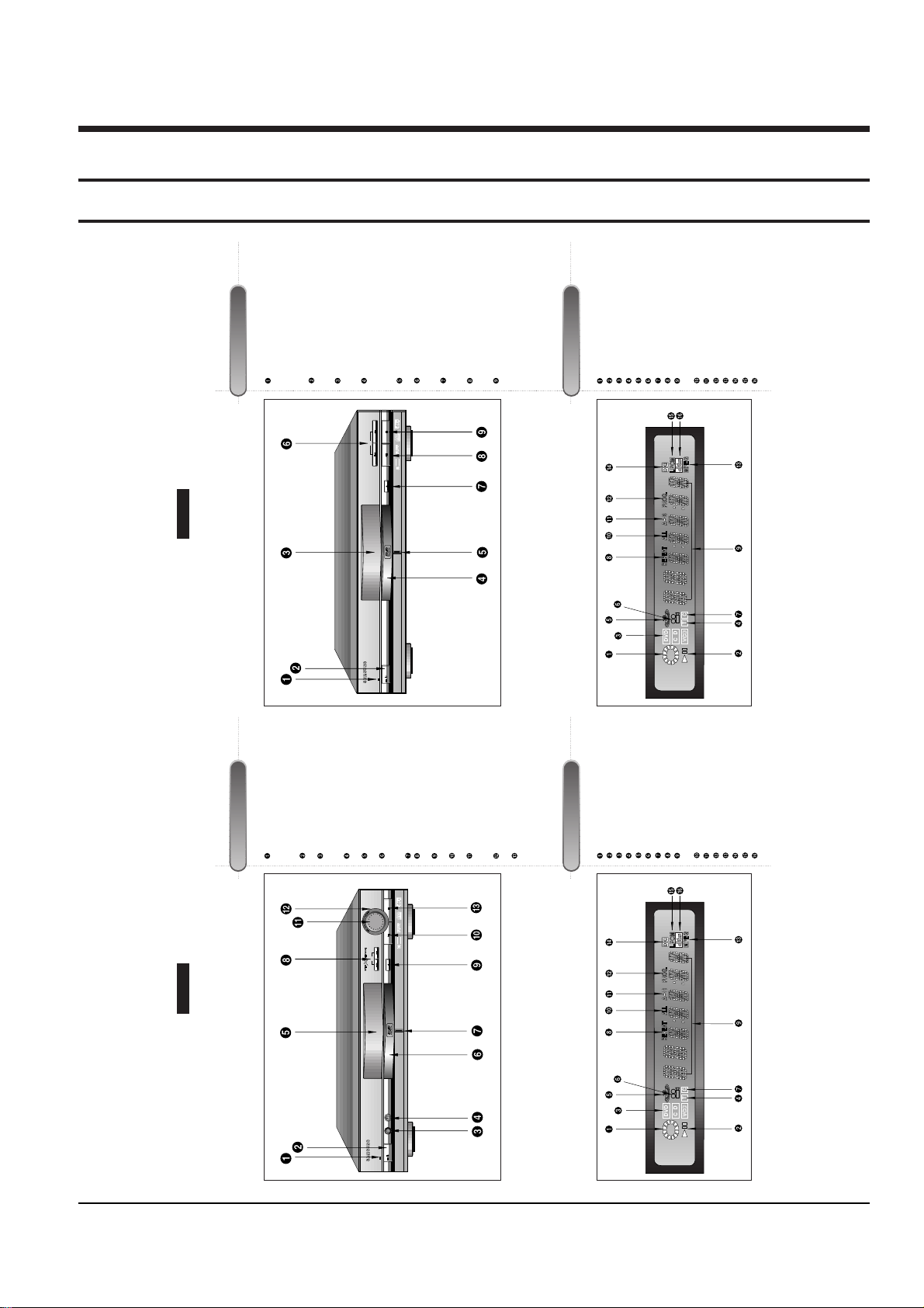
Front Panel Controls
Description-Front Panel
DVD-909
Front Display
STANDBY LAMP
• When the unit is first plugged in, the indi-
cator lights. When power is pressed on,
the lamp goes out.
POWER
• Use to turn the power on and off.
HEADPHONES JACK
• You can attach headphones here for pri-
vate listening.
HEADPHONES VOLUME
• Use to adjust headphones volume level.
DISPLAY (See below)
• Operation indicators are displayed here.
DISC TRAY
• Press OPEN/CLOSE to open and close
the disc tray.
GREEN LAMP
SKIP/SEARCH
• Use to skip or search a scene or music.
OPEN/CLOSE
• Press to open and close the disc tray.
PLAY/PAUSE
• Begin or pause disc play.
JOG DIAL
• Operates frame by frame playback. In
CD mode, performs track search.
SHUTTLE DIAL
• Performs fast or slow motion playback.
STOP
• Stops disc play.
DISC OPERATION ROTARY INDICATOR
OPERATION INDICATOR
DISC TYPE INDICATOR
TRACK INDICATOR
3D SOUND INDICATOR
ANGLE INDICATOR
CHAPTER INDICATOR
REPEAT INDICATOR
CHAPTER, TITLE, TRACK & MESSAGE
INDICATOR
ALL REPEAT INDICATOR
A-B REPEAT INDICATOR
PROGRAM PLAYINDICATOR
MPEG INDICATOR
DOLBY DIGITAL INDICATOR
LINEAR PCM INDICATOR
DTS INDICATOR
Description-Front Panel
DVD-709
Front Panel Controls
Front Display
STANDBY LAMP
• When the unit is first plugged in, the indi-
cator lights. When power is pressed on,
the lamp goes out.
POWER
• Use to turn the power on and off.
DISPLAY (See below)
• Operation indicators are displayed here.
DISC TRAY
• Press OPEN/CLOSE to open and close
the disc tray.
GREEN LAMP
SKIP/SEARCH
• Use to skip or search a scene or music.
OPEN/CLOSE
• Press to open and close the disc tray.
PLAY/PAUSE
• Begin or pause disc play.
STOP
• Stops disc play.
DISC OPERATION ROTARY INDICATOR
OPERATION INDICATOR
DISC TYPE INDICATOR
TRACK INDICATOR
3D SOUND INDICATOR
ANGLE INDICATOR
CHAPTER INDICATOR
REPEAT INDICATOR
CHAPTER, TITLE, TRACK & MESSAGE
INDICATOR
ALL REPEAT INDICATOR
A-B REPEAT INDICATOR
PROGRAM PLAYINDICATOR
MPEG INDICATOR
DOLBY DIGITAL INDICATOR
LINEAR PCM INDICATOR
DTS INDICATOR
DIGITAL VIDEO
SKIP
N-2-2
SPATIALIZER
OPEN/
CLOSE
OPEN/
CLOSE
DVD/VIDEO-CD/CD PLAYER DVD-709
POWER
STANDBY
24bit 96kHz AUDIO D/A CONVERTER
DIGITAL VIDEO
N-2-2
SPATIALIZER
SKIP
OPEN/
CLOSE
OPEN/
CLOSE
OPEN/
CLOSE
DVD/VIDEO-CD/CD PLAYER DVD-909
LEVEL
PHONE
POWER
STANDBY
MIN MAX
ADVANCED DOLBY DIGITAL DECODER BUILT-IN
Operating Instructions
4-2 Samsung Electronics
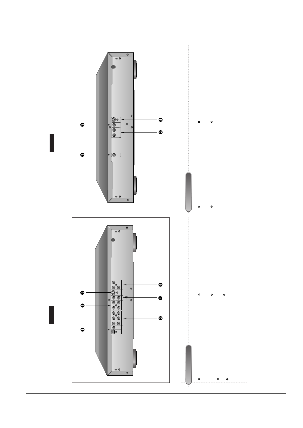
Description-Rear Panel
DVD-909
Rear Panel
DIGITAL AUDIO OUT JACK
• Use either an optical or coaxial digital cable to connect to a
compatible Dolby Digital receiver. Use to connect to an A/V
Amplifier that contains the Dolby Digital decoder or DTS
decoder.
5.1CH ANALOG AUDIO OUTJACKS
• Connect to an amplifier with 5.1ch analog input jacks.
MIXED AUDIO OUT JACKS
• Connect to the Audio input jacks of your television, audio/video
receiver, or VCR.
VIDEO OUT JACKS
• Use a video cable to connect one of these jacks to the Video
input on your television.
S-VIDEO OUT JACK
• Use the S-Video cable to connect this jack to the S-Video jack
on your television for a higher quality picture.
COMPONENT VIDEO OUT JACKS
• Use these jacks if you have a TV with component video in
jacks. These jacks provide Pr, Pb and Yvideo. Along with S-
Video, Component Video provides the best picture quality.
Description-Rear Panel
DIGITAL AUDIO OUT JACK
• Use a coaxial digital cable to connect to an A/V Amplifier that
contains a Dolby Digital decoder or DTS decoder.
ANALOG AUDIO OUT JACKS
• Connect to the Audio input jacks of your television, audio/video
receiver, or VCR.
VIDEO OUT JACK
• Use a video cable to connect this jack to the Video input on
your television.
S-VIDEO OUT JACK
• Use the S-Video cable to connect this jack to the S-Video jack
on your television for a higher quality picture.
DVD-709
Rear Panel
VIDEO OUT S-VIDEO OUT
R L
ANALOG AUDIO OUT
DIGITAL
AUDIO OUT
YPb
COMPONENT VIDEO OUT
Pr
V1
V2
VIDEO OUT S-VIDEO OUT
L1
L2
R2
S/W
CENTER R1
R FRONT L
R SURROUND L
DIGITAL AUDIO OUT ANALOG AUDIO OUT MIXED AUDIO OUT
OPTICAL COAXIAL
Operating Instructions
Samsung Electronics 4-3
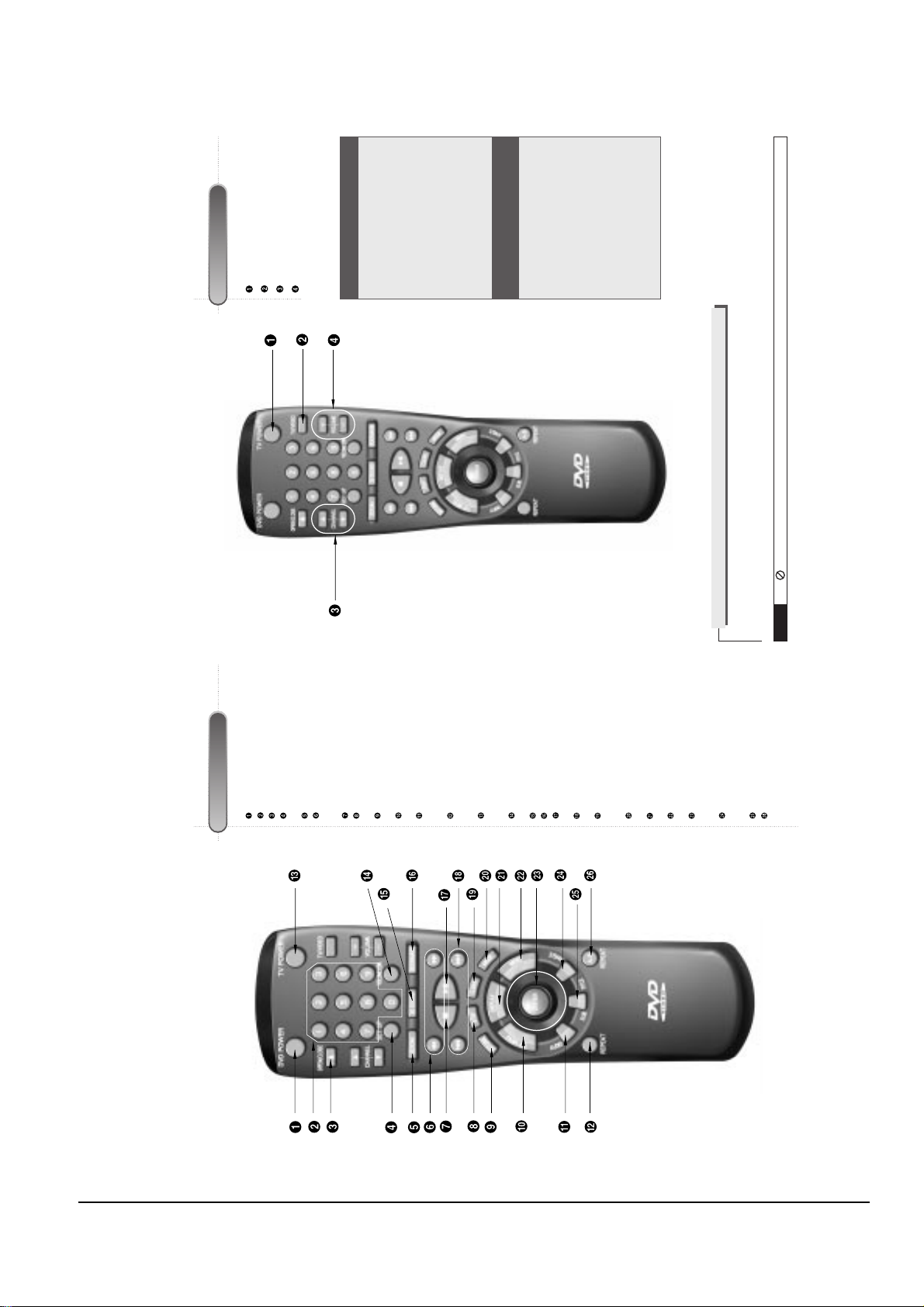
ATour of the Remote Control
DVD Function Buttons
DVD POWER Button
NUMBER Buttons
OPEN/CLOSE Button
SETUP Button
• Brings up the DVD player’s Setup menu.
ZOOM Button
SEARCH Buttons
• Allows you to search forward/backward
through a disc.
STOP Button
STEP Button
• Advances playback one frame at a time.
RETURN Button
• Returns to a previous menu.
TOP MENU Button
• Accesses a music or video display directly.
AUDIO Button
• Use this button to access various audio
functions on a disc.
REPEAT Button
• Allows you to repeat play a title, chapter,
track, or disc.
TV POWER Button
• Use to set the remote to control a compati-
ble TV.
VOLUME CON. Button
• To control the master volume of the player.
3D SOUND Button
BOOKMARK Button
PLAY/PAUSE Button
• Begin/Pause disc play.
SKIP Buttons
• Use to skip the title, chapter, or track.
CLEAR Button
• Use to remove menus or status displays
from the screen.
MODE Button
• Allows you to program a specific order.
DISPLAYButton
• Displays the current disc mode.
MENU Button
• Brings up the Disc menu.
ENTER/DIRECTION Button
(UP/DOWN or LEFT/RIGHT Button)
• This button functions as a toggle switch.
ANGLE Button
• Use to access various camera angles on a
DVD.
SUBTITLE Button
A-B REPEAT Button
• Use to mark a segment to repeat between
A and B.
ATour of the Remote Control (Cont’d)
TV Function Buttons
TV POWER Button
TV/VIDEO Selection Button
CHANNEL UP/DOWN Buttons
VOLUME UP/DOWN Buttons
NOTE
This icon indicates an invalid button press.
If remote doesn’t operate
properly:
1.
Open the battery cover on
the back of the remote.
2.
Insert two AAbatteries.
Make sure that the polari-
ties (+ and -) are aligned
correctly.
3.
Replace the battery cover.
• Check the polarity + - of the
batteries (Dry-Cell)
• Check if the batteries are
drained.
• Check if remote sensor is
blocked by obstacles.
• Check if there is any fluores-
cent lighting nearby.
Install Batteries in the Remote
To Connect Headphones (not included) (DVD-909 only)
Connect headphones with a standard stereo plug to the headphone jack (M6).
• Before connecting, set headphone volume at minimum. Then adjust to a suitable volume.
Operating Instructions
4-4 Samsung Electronics
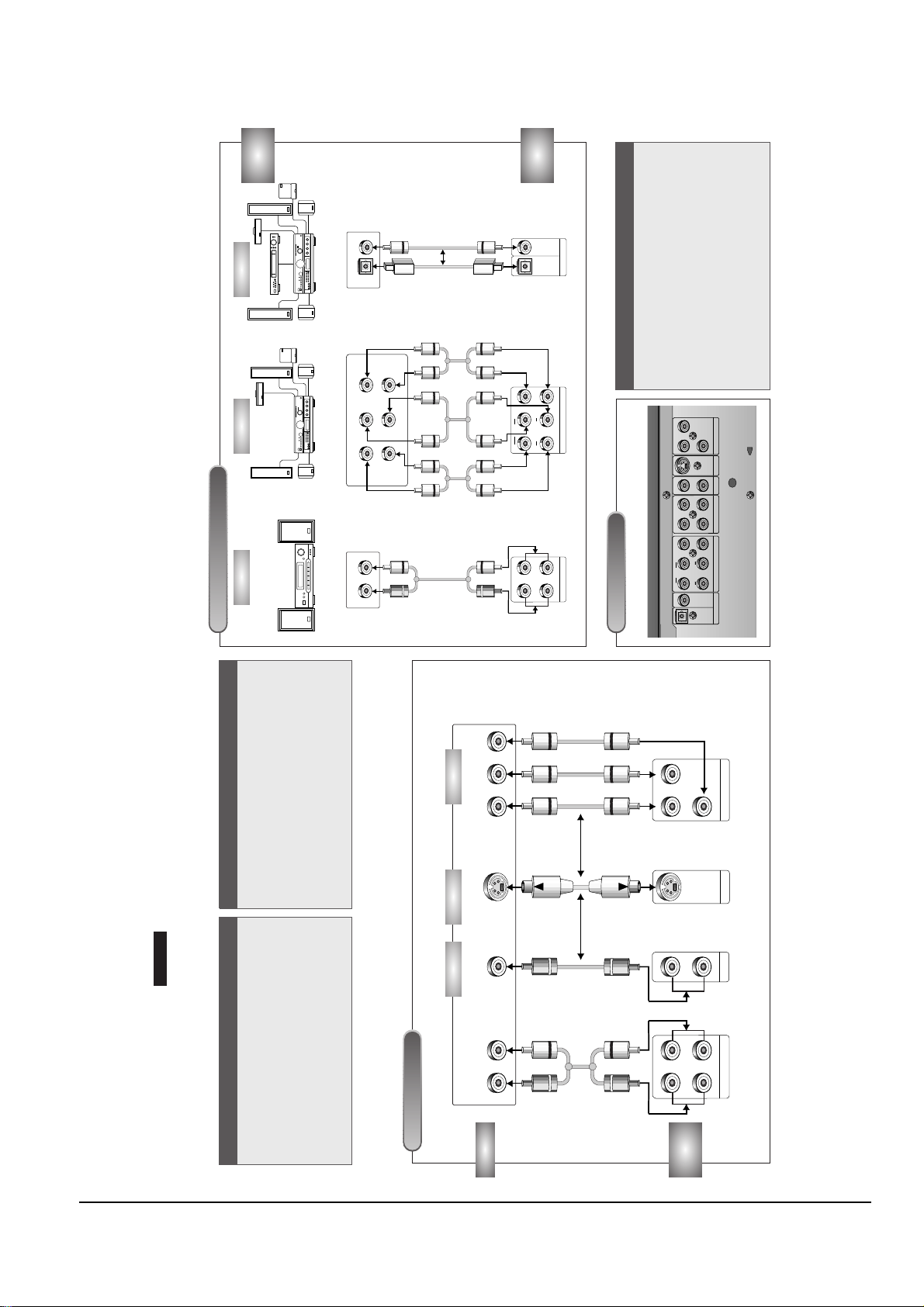
Choosing a Connection
The following show examples of connections commonly used to connect the DVD player with a TV and other
components.
DVD-909
Before Connecting the DVD Player Connecting to a TV (For Video)
MIXED AUDIO OUT
R1
R2
L1
R L
L2
COMPONENT VIDEO OUT
Y
Y
PbPbPr
Pr
VIDEO OUT
S-VIDEO OUT
V1
V2
TV
DVD
PLAYER
Connecting to a TV
• Method 1
DVD Player + TV with Video Input Jack
• Method 2
DVD Player + TV with S-Video Input Jack
• Method 3
DVD Player + TV with Component Video Jacks
• Always turn off the DVD player, TV, and other
components before you connect or disconnect any
cables.
• Refer to owner’s manual of the components you
are connecting for more information on those par-
ticular components.
TV (Normal, Widescreen, Projection, etc..)
Audio Input Jacks
Good
pictureBasic Audio
OR
OR
AV Cable
(included)
S-Video
Cable
(included)
Video Cables
(not included)
Better
picture Best picture
Video Input Jack S-Video Jack Component Video Jacks
Method 1 Method 2 Method 3
MIXED AUDIO OUT
R1
R2
L1
R L
L2
ANALOG AUDIO OUT
R FRONT L
R SURROUND L
CENTER
S/W
OPTICAL COAXIAL
OPTICAL COAXIAL
DIGITAL AUDIO OUT
C
hoosing a Connection (Cont’d)
Connecting to an Audio System
AUDIO
SYSTEM
DVD
PLAYER
Connecting to an Audio System
Rear Panel
• Method 1
DVD Player + 2ch Stereo Amplifier or
Dolby Pro Logic Decoder
• Method 2
DVD Player + Amplifier with 5.1ch
Analog Input Jacks
• Method 3
DVD Player + Amplifier with Dolby
Digital Decoder/DTS Decoder
Method 1 Method 2 Method 3
Mixed Audio Out Analog Audio Out
Audio Input JacksAudio Input Jacks
5.1ch Analog Amplifier Dolby Digital Decoder
Digital Audio Input Jacks
2ch Amplifier
Digital Audio Out
OPTICAL COAXIAL
DIGITAL AUDIO OUT ANALOG AUDIO OUT MIXED AUDIO OUT
VIDEO OUT S-VIDEO OUT
V1
V2
COMPONENT VIDEO OUT
YPb
Pr
R FRONT L
R SURROUND L
CENTER R1
R2
L1
L2
S/W
Front (RH)
Rear (RH)
Front (LH)
Rear (LH)
Center
Subwoofer
OR
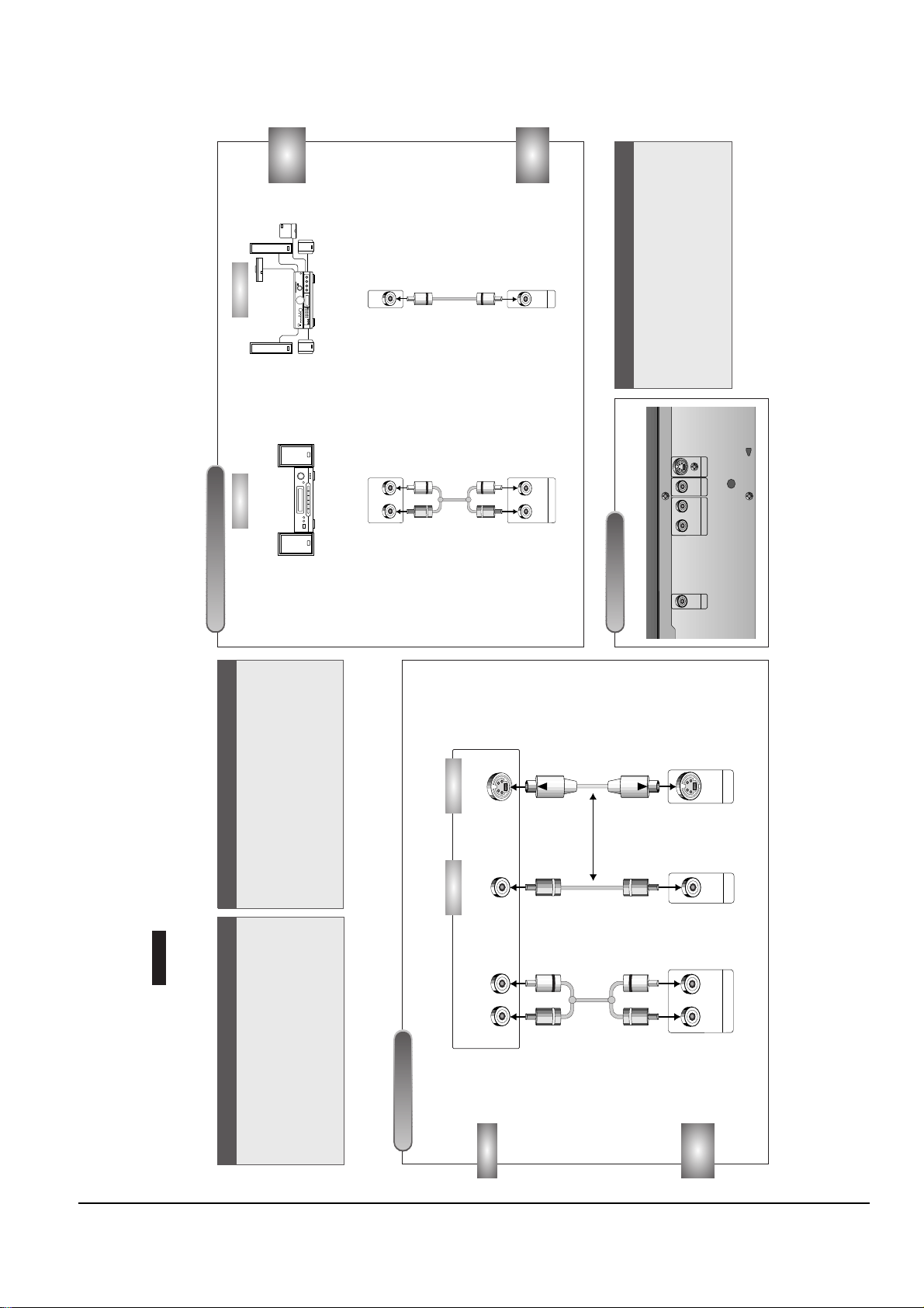
Operating Instructions
Samsung Electronics 4-5
Choosing a Connection
The following show examples of connections commonly used to connect the DVD player with a TV and other
components.
DVD-709
Before Connecting the DVD Player Connecting to a TV (For Video)
R L
ANALOG AUDIO OUT
R L
VIDEO OUT
S-VIDEO OUT
TV
DVD
PLAYER
Connecting to a TV
• Method 1
DVD Player + TV with Video Input Jack
• Method 2
DVD Player + TV with S-Video Input Jack
• Always turn off the DVD player, TV, and other
components before you connect or disconnect any
cables.
• Refer to owner’s manual of the additional compo-
nents you are connecting for more information for
those particular components.
AV Cable
(included)
S-Video Cable
(included)
Better
picture
Basic Audio
Best
picture
Video Input Jack
Audio Input Jacks
S-Video Jack
Method 1 Method 2
TV (Normal, Widescreen, Projection, etc..)
OR
Choosing a Connection (Cont’d)
DIGITAL
AUDIO OUT
R L
ANALOG AUDIO OUT
R L
AUDIO
SYSTEM
DVD
PLAYER
Connecting to an Audio System
Method 1 Method 2
Analog Audio Out
Audio Input Jacks
Digital Audio Input Jack
Dolby Digital Decoder2ch Amplifier
Digital Audio Out
Rear Panel
DIGITAL
AUDIO OUT
ANALOG AUDIO OUT
R L
VIDEO OUT S-VIDEO OUT
Connecting to an Audio System
• Method 1
DVD Player + 2ch Stereo Amplifier or Dolby Pro
Logic Decoder
• Method 2
DVD Player + Amplifier with Dolby Digital
Decoder/DTS Decoder