

Page 1
DLP Training
(Atlantis Chassis)
March 2004
Page 2
Agenda
1. Power Supply
2. Digital Board
3. Analog Board
4. DMD Board
5. Troubleshooting
6. Initialization Process
7. LED Indicators
8. Optical Section
9. Service Hints
10. Parts Information
11. Dimensions
12. Review
Page 3
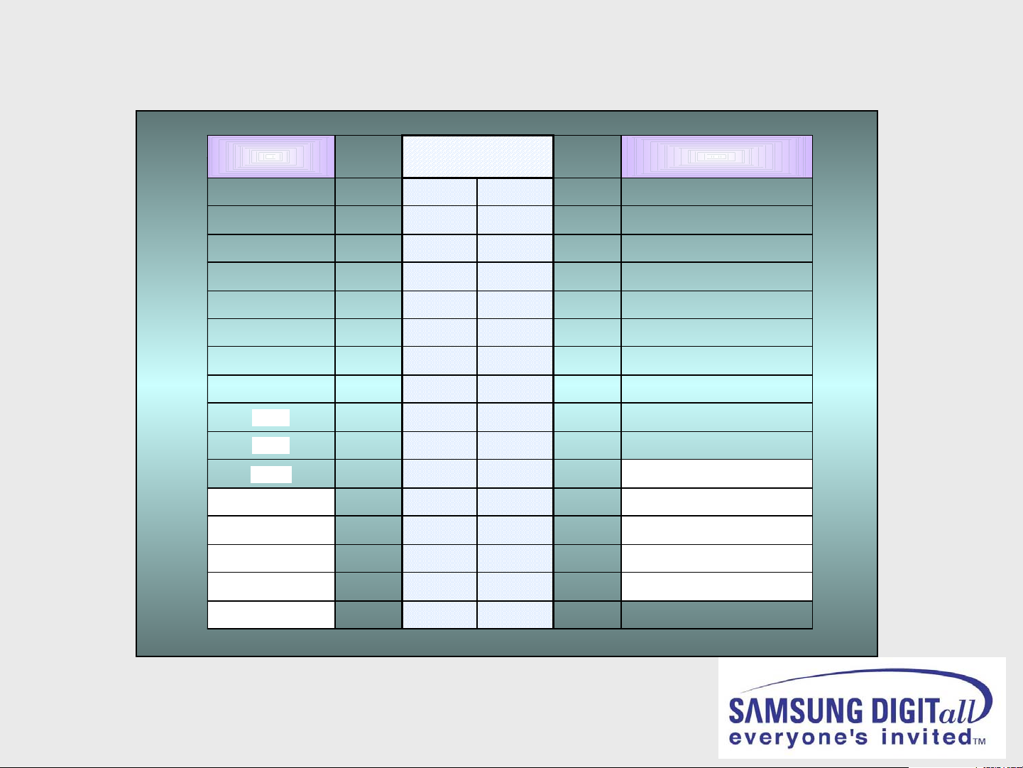
Power Supply Board
CN803
Pin #
Spec
Used
Pin #
Spec
Pin #
A
Power
-Mute
GND33VBGND5V
-S/W
Supplies DC voltage to the PCB ANALOG
CN802
S14.
5VB
S-
GND
S14.
5VB
S-
GND
12 13109118
5.7
VB
7654321
N.CN.C.Power
GN
D
7654321
CN 803
Spec
Used
GND12VB
B
Supplies DC voltage to the PCB ANALOG
70VBGNDGND12V
CN 802
Page 4
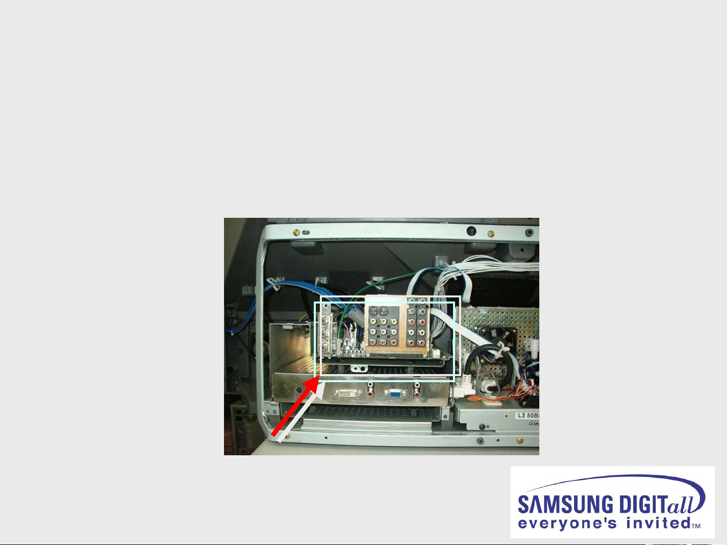
Digital Board
• Microprocessor (Generates turn on signal to power board)
• Monitor LED’s
• All Digital Video Processing
• Sensor / Switch Controls
• OSD / Menu
RS232- Factory Use Only
HDMI- A/V Input
RGB-PC Input
DVI – Digital Visual Interface
Page 5
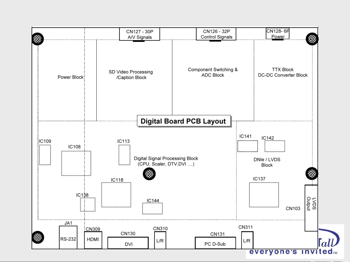
Digital Board Layout
Page 6
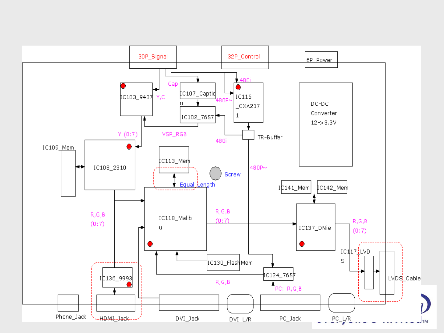
Digital Board Characteristics
Page 7
Analog Board
• Distributes supply voltage from the Power Board to Digital Board
• Transfers Turn-On Command from Digital Board to Power Board.
• Encompasses the majority of the Audio Circuit
• Analog Video Switching / Processing
Page 8
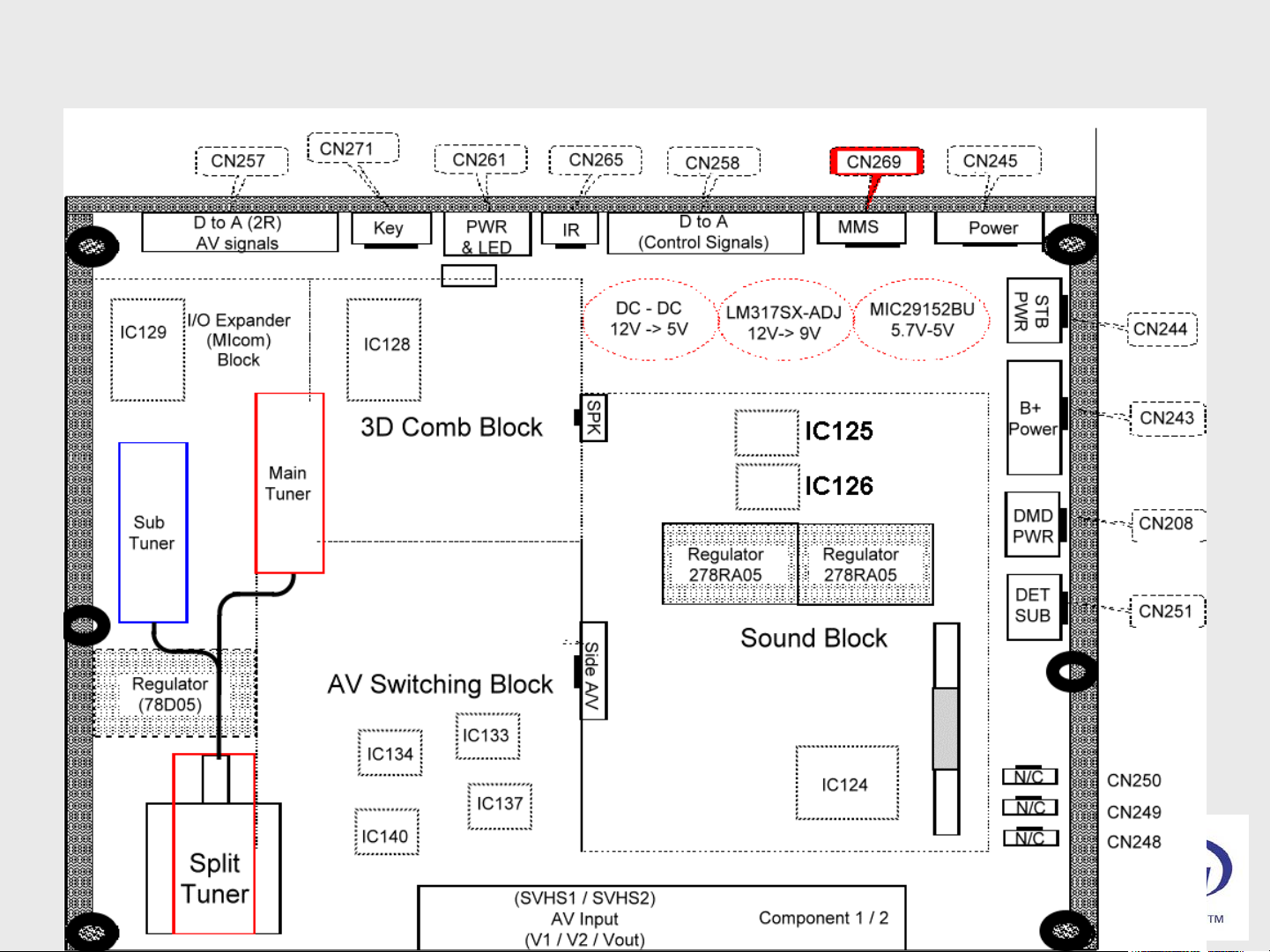
Analog PCB Layout
Page 9
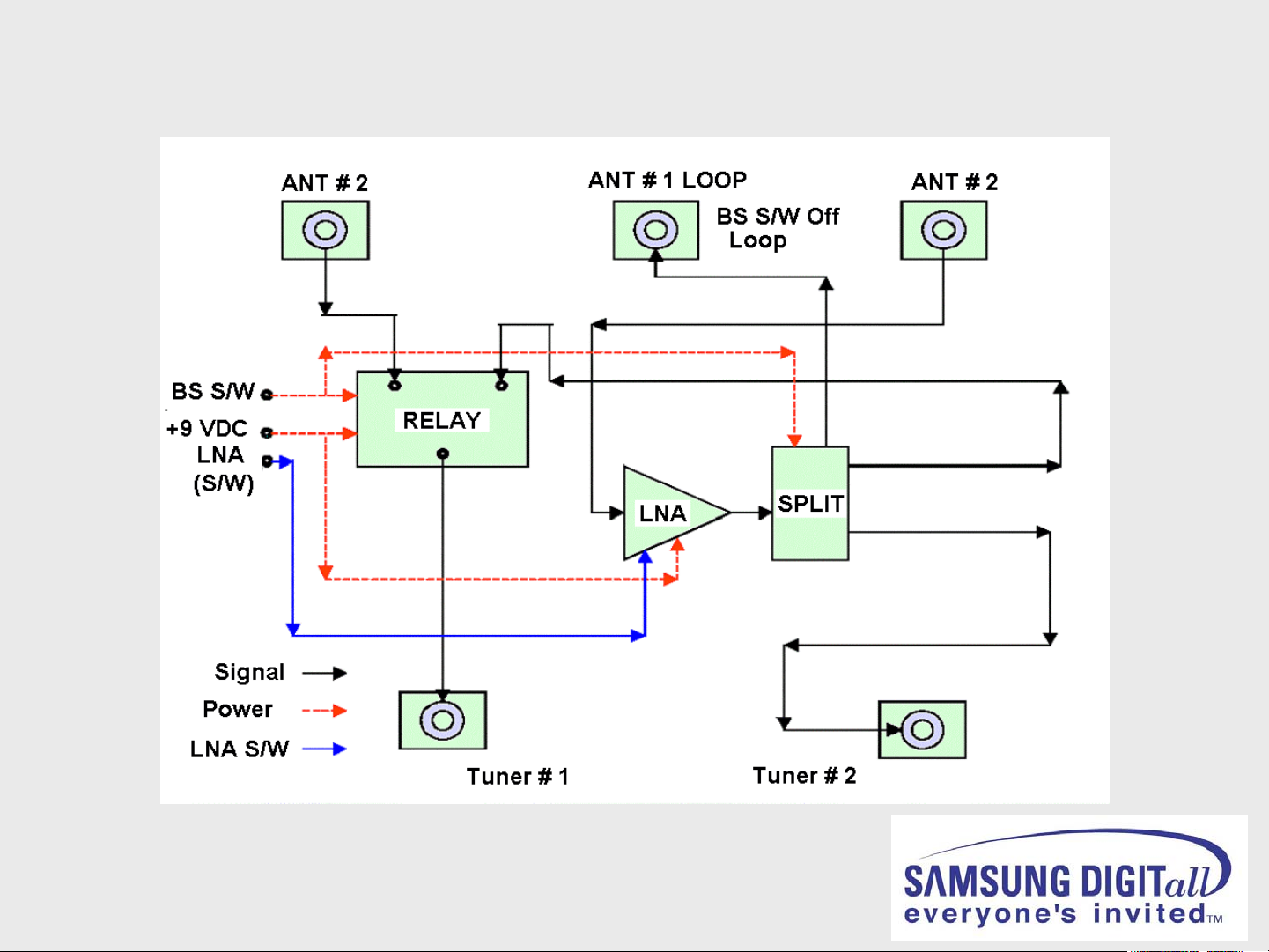
Analog Board Block Diagram
RF SWITCH (LNA) BLOCK
Page 10
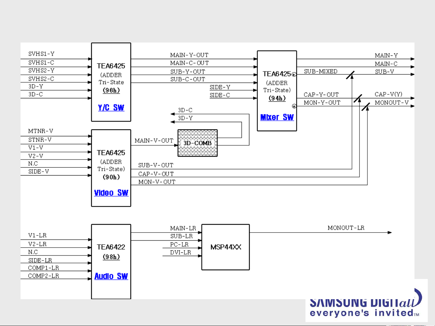
AV Switching (TEA64XX) Block
Page 11
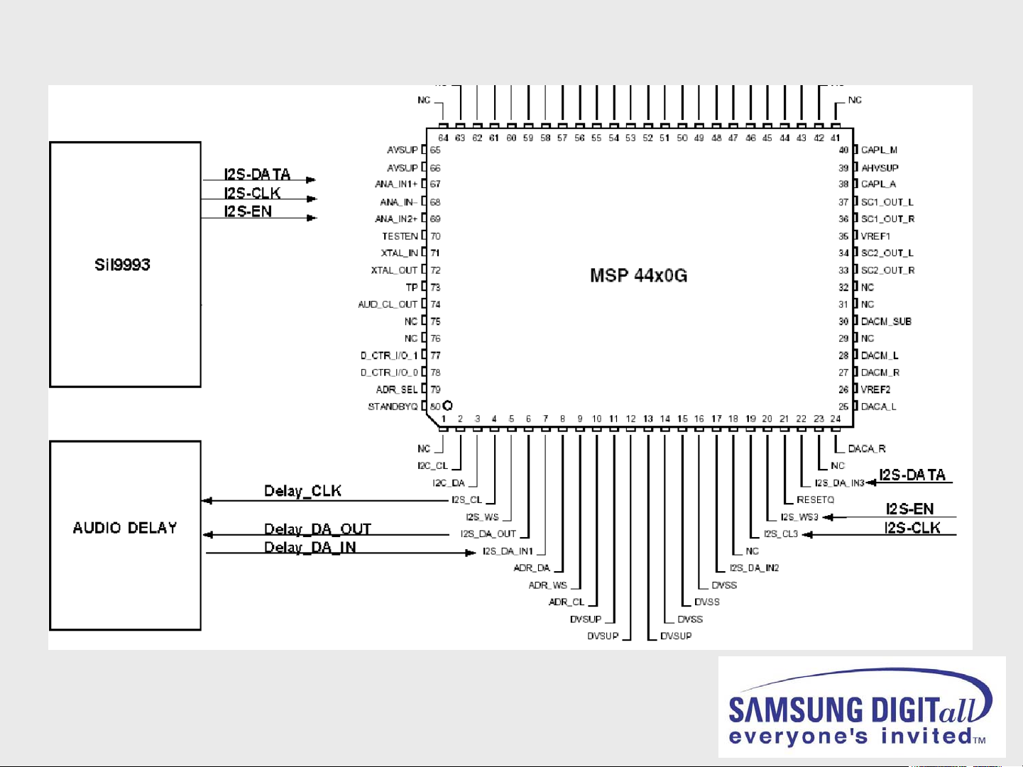
Audio Delay and HDMI Audio
Page 12
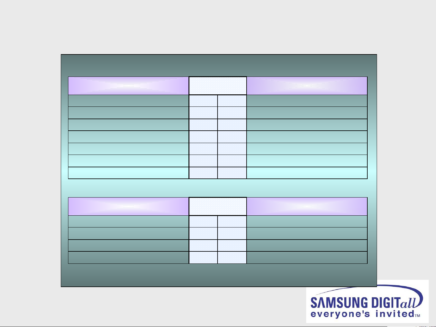
CN 257 Pin Assignment
CN257- Supplies AV Signals to PCB DIGITAL
Pin Name I/O PIN No. I/O Pin Name
Comp1-Y
Comp1-Pb
Comp1-Pr
Comp2-Y
Comp2-Pr
Comp2-Pb
N.C.
N.C.
N.C.
Main-Y/V
Main-C
Sub-Y/V
Sub-C
Caption-CVBS
IR
←
←
←
←
←
←
←
←
←
←
←
←
←
←
←
1 2 GND
3 4 GND
5 6 GND
7 8 GND
9 10 GND
11 12 GND
13 14 GND
15 16 GND
17 18 GND
19 20 GND
21 22 GND
23 24 GND
25 26 GND
27 28 GND
29 30 GND
Page 13
CN258 Pin Assignment
CN258- Connects Control Signals between PCB Analog and PCB Digital
Pin Name I/O PIN No. I/O Pin Name
LED1
LED2
LED3 5 6 GND
Key1
Key2 9 10
Reset-D
I2C-ST OP
Power-SW
N.C. 17 18
N.C.
GND
MCLK_AUDIO
S-MUTE
PC-L
PC-R 29 30 DVI-R
↔
→
←
←
←
←
←
←
→
→
→
1 2
3 4
7 8
11 12 GND
13 14
15 16 SCL-Digital
19 20
21 22 I2S-E N -H DMI
23 24 I2S-DATA-HDMI
25 26
27 28
↔
←
↔
←
←
←
←
←
←
SDA-Micom
SCL-Micom
SDA-Analog
SCL-Analog
SDA-Digital
GND
I2S-CLK-HDMI
GND
DVI-L
GND
←
31 32
←
GND
Page 14
CN243/CN244 Pin Assignment
CN243 / 244 Receives Power Signals from PCB POWER
Pin Name PIN No. Pin Name
Power-Mute 1 2 S14.5VB
S-GND 3 4 S14.5VB
S-GND 5 6 5.7VB
GND 7 8 12VB
GND 9 10 12VB
GND 11 12 70VB
GND 13 -
Pin Name PIN No. Pin Name
5VA 1 2 GND
33VB 3 4 GND
Power-SW 5 6 N.C.
N.C. 7 -
Page 15
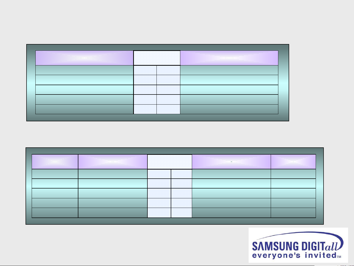
CN208 / CN251 Pin Assignment
CN208 Supplies Power Signals to PCB DMD
Pin Name PIN No. Pin Name
5VB 1 2 5VB
GND 3 4 GND
12VB 5 6 12VB
GND 7 8 GND
GND 9 - -
CN251 supplies power to Actuator / Protection Board
Pin Name SUB Detector/Actuator PIN No. SUB Detector/Actuator Pin Name
GND Ground 1 2 Fan-VCC 12VB
GND Ground 3 4 SDA-Memory SDA-M
SCL-M SCL-Memory 5 6 Ground GND
5VA 5VA 7 8 Ground GND
70VB 70VB 9 10 Ground GND
Page 16
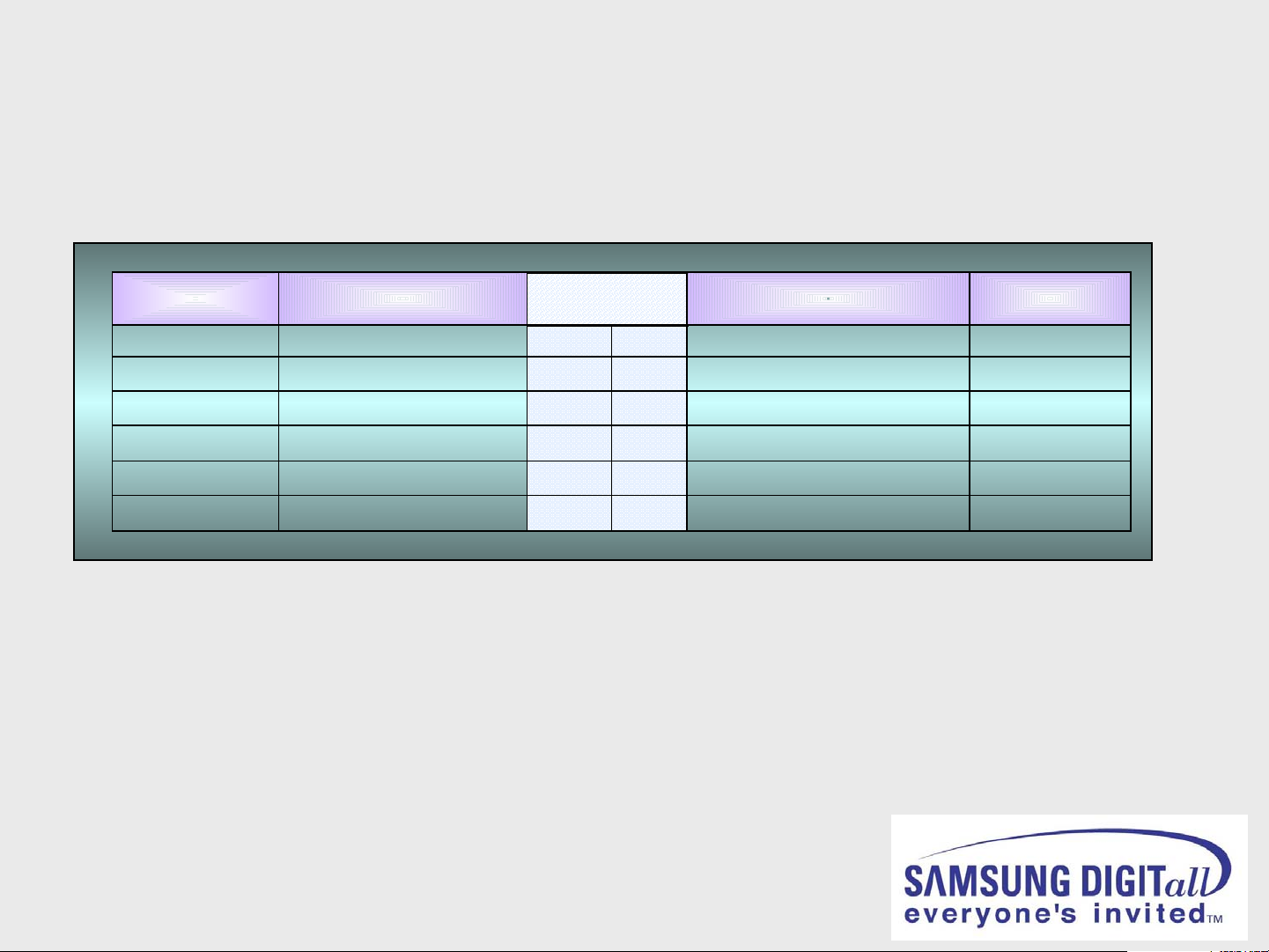
CN223 Pin Assignment
CN223 Receives AV Signals from PCB SIDE-AV
Pin Name Side AV PIN No. Side AV Pin Name
Side-Y SVHS Y (Luma) 1 2 SVHS C (Chroma) Side-C
GND Ground 3 4 Video (CVBS) Side-V
GND Ground 5 6 Side Sound L Side-L
GND Ground 7 8 Side Sound R Side-R
GND Ground 9 10 SVHS Jack Detect Side-SDET
Side-VDET Video Jack Detect 11 -
Page 17
I/O Expander Pin Assignment
DES NAME PIN PIN NAME DES
GND VSS 1
XIN 2 31 P0.2 I/O S1-DET
XOUT 3 30 P0.3 I/O S2-DET
GND TEST 4 29 P0.4 I/O,ADC Side-SDET
Comp2-DET I/O P0.1 5 28 P0.5 I/O,ADC V1-DET
Comp1-DET I/O P0.0 6 27 P0.6 I/O,A D C V2-DET
RESET-D RESET 7 26 P0.7 I/O,A DC Side-VDET
S
3
P
9
4
32 VDD
2
RF-SEL O P3.0 8 25 P3.1 O SOUND-RESET
8
LNA-SW O P3.2 9 24 P3.3 O DEFAULT
MTNR-AFT I/O,A D C P2.0 10 23 P1.0 I/O DELAY1
STNR-AFT I/O,A D C P2.1 11 22 P1.1 I/O DELAY2
N.C I/O,A DC P2.2 12 21 P1.2 I/O GAIN0
N.C I/O,A DC P2.3 13 20 P1.3 I/O GAIN1
RF-AGC I/O,A DC P2.4 14 19 P2.7 SCL SCL-A
/
3
2
S
O
P
GND ADDRESS P2.5 15 18 P2.6 SDA SDA-A
GND AVSS 16 17 AVREF
Page 18

DMD Board
• Controls Lamp Turn-On
• Powers Color Wheel
Motor
• Drives DMD Panel
• Sensor Controls
• Attached to Light Engine
Page 19

DMD Block Diagram
Page 20

Troubleshooting
Page 21

OP101
OP101
Dead Set
Check power
to analog
board CN245
OK
Unplug
connector
CN245 if LED
(OP103)
turns on
replace the
digital board
Is 5V standby
LED(OP103) lit
on analog board?
Yes
Make sure CN103
on digital board
is connected
OK
Replace keypad
No
NG
NG
Reconnect CN103
Unplug the
Actuator
Board
OK
CN103
Replace the
Actuator
CN103
NG
Replace the
Power
board
Page 22

CN106
CN106
Blinking Temp LED
Check Temp Sensor
connector CN106
on Actuator Board
OK
NG
Re-insert
connector
Install jumper across
Temp Sensor Terminals.
Does it work?
Yes
Replace Temp Sensor.
No
Temp Sensor
Temp Sensor
Replace
the Actuator board
Page 23

Blinking Temp and Timer LED
Yes
Are fans running?
Replace Actuator board
No
Check for 8VDC
voltage(s) at CN103,104
on Actuator Board
NG
Check CN802 pin 8,10
on Power board for 12VB
OK
Replace
NG
OK
Replace fan(s)
NG
Remove power and
check the DMD,
Actuator and Digital
boards for short
circuit on the 12V
line to ground.
the Actuator
board
Page 24

All Front Panel LEDs Blinking
All three LEDs blinking is the most common failure indication. It can be caused by
defective lamp, defective color wheel, fan failure or other defective components.
wheel assembly
Replace
NO
Replace color
NG
OK
OK
Does color
wheel run?
YES
If Lamp is on
with no Video,
Check
Is lamp on?
YES
NO
See next page
DMD BOARD
connector
CN103 on the
Digital board
Page 25

All Front Panel LEDs Blinking Continued
NO
Does lamp
come on, then
shut off?
Check 220-280V dc to lamp ballast (CN1)
Replace Power Board
OK
Replace lamp
assembly
Check pin 2 on CN504 (lamp enable)
Measure with DC meter
NG
Re-install
lamp assembly
NG
OK
on DMD Board for 5V p-p (90Hz).
NG
Replace
OK
YES
Check 0V dc at
CN504
(lamplitz) pin 5
on DMD Board
OK
Replace
ballast or
assembly
NG
lamp
or ballast
DMD Board
Page 26

Blinking Lamp and Temp. LED’s
Is lamp
cover installed?
Yes
Make sure lamp cover
switch is activating
OK
Short CN107
Check boss
NG
No
Install lamp cover
CN107
CN107
on Actuator Board
Replace the Actuator board
on Lamp Cover
NG
Page 27

Initialization Process
Standby LED
1. Standby LED on Analog PCB ON (5V)
2. Power ON signal from Sub Front PCB or IR sensor
to Digital PCB.
3. Power ON signal generated by Digital PCB->
Analog PCB-> POWER PCB.
4. All other voltages turn on (3 status LED’s on
analog board lit) .
5. Fans turn on.
6. Fan protection circuit verifies Fan Operation.
7. Digital PCB tells DMD PCB to turn color wheel and
lamp on.
8. DMD / digital PCB’s check feedback (LampLitz –
low, DDP ready – High) signals from lamp and DMD
Controller (DDP1011).
9. If OK, Digital PCB tells DMD to remove video mute.
Page 28

Front Panel LED Indicators
Legend
¦ = LED On
|= LED Off
= LED Blinking
Timer Lamp Standby/
Temp
| | ¦ Standby State
¦ | | Auto Timer On/Off has been set
| | | Set is operating Normally
| | Turn on state, picture will appear in about 15 seconds
| Auto Timer On/Off has been set, picture will appear in ~ 25
| A cooling fan inside the set is not operating properly
| The Lamp cover on the rear of the set is not installed properly.
| | Excessive Temperature error, check for proper ventilation
Indication
seconds
Lamp does not light, replace with a new lamp
Page 29

Optical Section
Page 30

Background
Samsung introduced their new DLP technology projection televisions in
2002. DLP stands for
Digital Light Processing
DLP is quite different than conventional projection television, which uses
three separate color CRT’s. These separate video signals are projected
and combined on the screen. DLP, on the other hand, has no CRT’s.
Instead, one high intensity lamp is used to project one image on the
screen.
DLP technology was first developed by Texas Instruments.
The heart of this technology is the DMD, or
Digital Micromirror Device.
Page 31

L2 and L3 Design Comparison
DMD PANEL
Incident light
1280 X 720
(921600 pixels)
Incident light
L2 Design : HD2 Panel
0.79
* Unit = Inch
L3 Design : HD3 Panel
Diamond Pixel Pattern
640 x 720
(460800 pixels)
* Unit = Inch
Page 32

Incident light
DMD Differences
1280 X 720
(921600 pixels)
Incident light
640 x 720
(460800 pixels)
0.79
Focus
Adjust
Focus
Adjust
Page 33

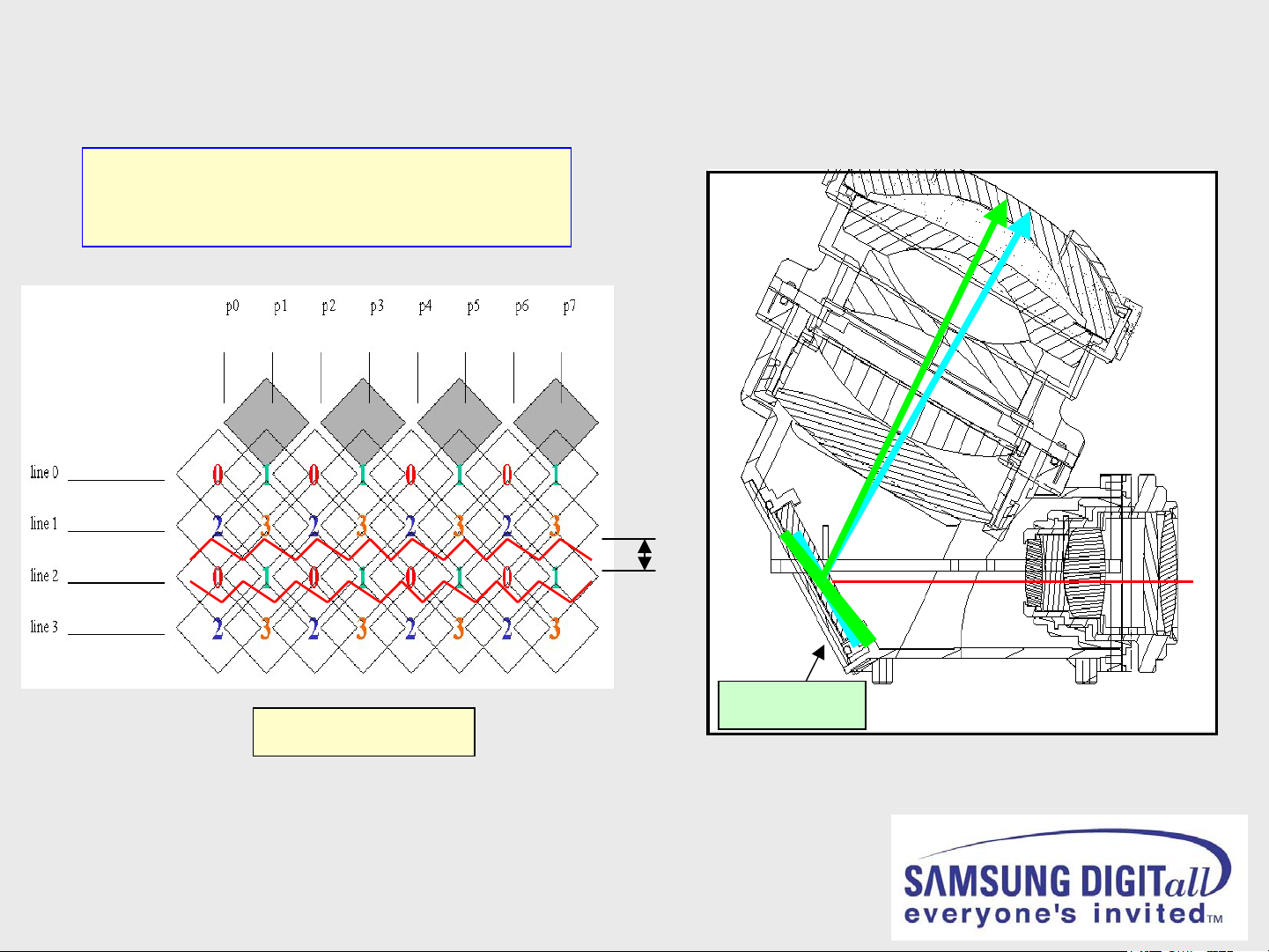
1. Display Resolution
p0 p1 p2 p3 p4 p5 p6 p7
p0 p1 p2 p3 p4 p5 p6 p7
1
1
1
line 0
line 0
line 1
line 1
line 2
line 2
line 3
line 3
1
1
2
2
2
1 1 1 1
1 1 1 1
2 2 2 2
2 2 2 2
2
2
2
Low Resolution
1
1
1
2
2
Design Concept
Frame 1 Frame 2
p0 p1 p2 p3 p4 p5 p6 p7
p0 p1 p2 p3 p4 p5 p6 p7
line 0
line 0
line 1
line 1
line 2
line 2
line 3
line 3
Driving Actuator
=
1
1
1
2
2
2
2
1 1 1 1
1 1 1 1
2 2 2 2
2 2 2 2
1
1
1
2
2
line 0
line 0
line 1
line 1
line 2
line 2
line 3
line 3
1
1
2
2
2
2
0 0 0 0
0 0 0 0
2 2 2 2
2 2 2 2
p0 p1 p2 p3 p4 p5 p6 p7
p0 p1 p2 p3 p4 p5 p6 p7
0 0 0 0
0 0 0 0
3 3 3 3
+
p0 p1 p2 p3 p4 p5 p6 p7
p0 p1 p2 p3 p4 p5 p6 p7
1
1
2
3
2
3
1 1 1 1
1 1 1 1
3 3 3 3
3 3 3 3
3 3 3 3
0 0 0 0
0 0 0 0
3 3 3 3
3 3 3 3
1
1
3 3 3
3 3 3
1
1
2
2
10 0 0 0
10 0 0 0
2
2
( dr iven to bla ck)
( dr iven to bla ck)
High Resolution
X2 RESOLUTIONX1 RESOLUTION
Page 34
Realizing Method
Mirror movement by vibration of
Mirror movement by vibration of
Piezoelectric material.
Piezoelectric material.
Vibration Distance = ½ Pixel
X2 Resolution
460800 pixels -> 921600 pixels
Effect = Jagged line to Smooth line
Actuator
Folding Mirror VibrationFolding Mirror Vibration
Page 35

Light Engine Breakdown
LAMP MODULE
OPTICAL MODULE
DMD MODULE
Page 36

Optical Module
PROJECTION LENS
COLOR WHEEL
LOCATION OF DMD
LIGHT TUNNEL
Page 37

NDF
Color Wheel
<Air Bearing Type Motor>
<Air Bearing Type Motor>
Life time : over 30,000 hrs (max 50,000 hrs)
Life time : over 30,000 hrs (max 50,000 hrs)
On/off : over 50,000 times (max 300,000 times)
On/off : over 50,000 times (max 300,000 times)
Less Vibration & Noise
Less Vibration & Noise
7
*Addition = Neutral Density Filter
NDF Purpose: Decrease Dither noise.
10,800
Page 38

60Hz
Actuator
SpecificationItemsNo.
79gMass1
0~0.015deg.Mirror tilt angle range2
Purpose: Smooth Picture
by ½ Pixel movement
using 60Hz mirror
vibration.
<1.0 mSecState transition time3
+/-0.025deg.Initial static angle4
Page 39

Lamp
Full name : High Pressure Mercury Lamp
Full name : High Pressure Mercury Lamp
Maker : Philips
Maker : Philips
Specification
Specification
Arc gap : 1.0 mm
Arc gap : 1.0 mm
Wattage : 100W or 120W
Wattage : 100W or 120W
Life time : about 8000 – 6000hrs
Life time : about 8000 – 6000hrs
Optical Specification
Optical Specification
Reflector type : E23
Reflector type : E23
Size : 95.25 +/-0.5mm
Size : 95.25 +/-0.5mm
Mount to focal point : 52mm
Mount to focal point : 52mm
(Reflector)
Bulb
Mount to Focal Point
Cover Glass
Page 40

Maker : Philips
Maker : Philips
Type no. : EUC 120PH/11
Type no. : EUC 120PH/11
Ignition : 20KV(Max 25KV)
Ignition : 20KV(Max 25KV)
Size : 150 x 60 x 32mm
Size : 150 x 60 x 32mm
Ambient temp. : under 65deg C.
Ambient temp. : under 65deg C.
Ballast
Page 41
Good Point :
Good Point :
1. Good Contrast
1. Good Contrast
2. No reflection of out-light.
2. No reflection of out-light.
3. Good View Angle (140 deg)
3. Good View Angle (140 deg)
4. Reduced Moire
4. Reduced Moire
5. Increased Screen Gain
5. Increased Screen Gain
Screen
Diffusion Plate
Diffusion Plate
High Brightness,
High Brightness,
High Contrast
High Contrast
Hard Coat
Hard Coat
Anti-static
Anti-static
function
function
Black Stripe(BS)
Black Stripe(BS)
Lenticular Lens
Lenticular Lens
155um
um
98
98um
61.9um
2.1mm
2.1mm
Lenticular Screen
Lenticular Screen
2.0mm
2.0mm
Fresnel Lens
Fresnel Lens
Page 42
Optical Specification
Parameter
Nominal
value
Commentunit
7-segment color wheel, TI
nits460Brightness
development board, no spoke
light recapture, reference lamp
Uniformity (ANSI)
-Typical
- Minimal
Contrast full on/off
–Typical
+/- 15
+/- 25
n.a.1500:1
%
%
+: brightest of 13 ANSI
points/average of 9 points
-: darkest of 13 ANSI
points/average of 9 points
7 segment color wheel,
TI development board, no
spoke light recapture
Page 43

Optical Specification Continued
Nominal
Parameter
value
Commentunit
Color Temperature
Projection distance
at 50” screen size
7,500 K
(Warm 1)
measured in image centern.a.
design valuen.a.≥ 2.6F-number
projection distance: distance from
mm585
mm30.98 mmExit pupil position
vertex of front lens to projection
screen
design value, distance to vertex of
front lens
design valuedeg.94F.O.V (Field of View)
Diamond Pixel Configurationmm12.451 x 7.008Panel size
Page 44
Optical Specification Continued
Nominal
Parameter
value
Commentunit
Lateral color aberration
@ 50” (R-G; B-G)
TV distortion
- in horizontal direction
- in vertical direction
≤ 7
≤ 8.5
≤ |0.3|
≤ |0.3|
µm
µm
%
%
Design value
440/546/640 nm
Pin Cushion or Barrel
condition
mechanical design valuedeg.66folding angle
Page 45
Service Hint #1
DMD BOARD ASSY
Problem : PIXEL DEFECT, VERTICAL LINE
Solution : Change the DMD Board assembly.
Vertical Line Problem (Jail Bar effect)
Pixel
Defect
Page 46

Service Hint #2
Color Wheel Assembly
13. Service Module
Problem : INCREASED NOISE
Solution : Change the Color wheel module.
Page 47
Service Hint #3
LAMP ASSY
Problem : LOW BRIGHTNESS or No Power
Solution : Change the Lamp module
Page 48
Service Hint #4
ACTUATOR
Problem : High Frequency Noise(1200Hz), Distorted edges in Picture
Solution : Change the Actuator
Actual
Page 49

Mechanic
Page 50
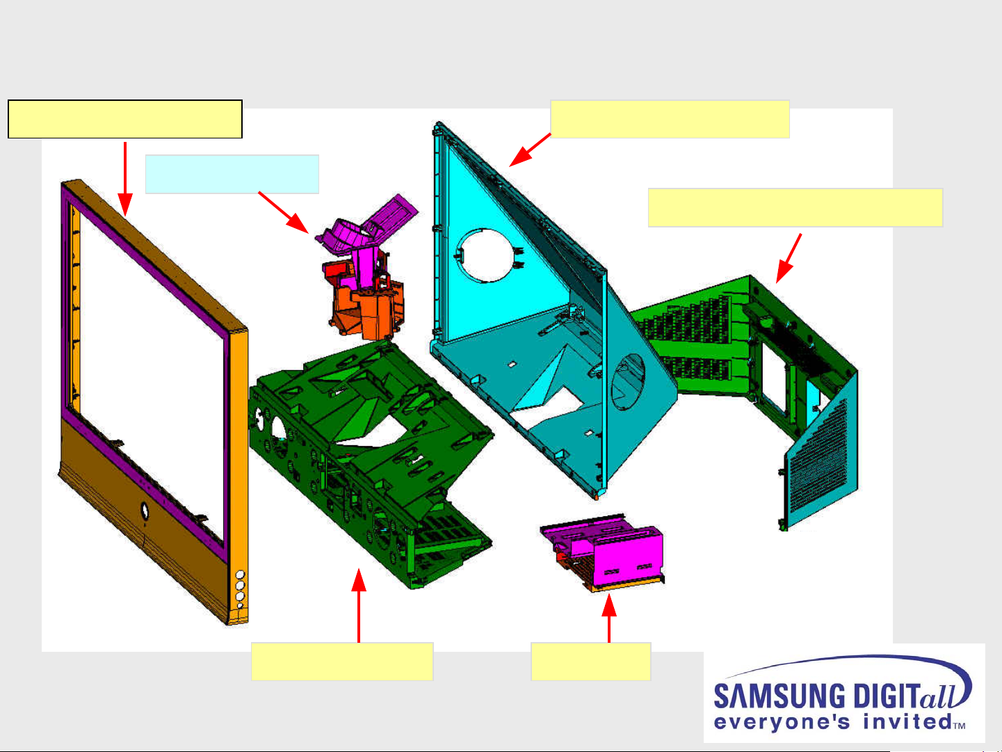
L3 DLP Main Parts
CABINET-FRONT
ENGINE ASSY
CABINET-BACK TOP
CABINET-BACK, BOTTOM
CABINET-MAIN
CHASSIS
Page 51

Set Dimensions
MODEL
46L3
50L3
56L3
61L3
MODEL
46L3
W x D x H
( mm Unit )
1094 x 339 x 814
1182 x 359 x 870
1330 x 396 x 963
1446 x 425 x 1035
Mirror Size
SIZE (W1 x W2 x H)
1035 x 530 x 523
Weight
(Kg)
31.5
35
41.5
45
W x D x H
( mm Box)
1205 x 455 x 950
1300 x 480 x 1010
1450 x 520 x 1105
1580 x 565 x 1170
Screen Size
MODEL
46L3
Weight
(Kg)
39
43
53
57
SIZE (W x H)
1021 x 580.5
50L3
56L3
61L3
1030 x 580 x 570
1279 x 650 x 645
1395 x 692 x 700
* Dimensions in mm
50L3
56L3
61L3
1126 x 646
1257 x 713.5
1381 x 790
Page 52

The End
Thank You!
Thank You!
 Loading...