

Page 1

2
CONTENTS
ⅠⅠ
.. SSPPEECCIIFFIICCAATTIIOONN
1. CAMERA SPECIFICATION …………………………………………………………………………………… 4
2. SYSTEM REQUIREMENT …………………………………………………………………………………… 5
3. LCD MONITOR INDICATOR ………………………………………………………………………………… 6
4. CONNECTION DIAGRAM …………………………………………………………………………………… 8
5. IDENTIFICATION OF FEATURES …………………………………………………………………………… 9
ⅡⅡ
.. IINNSSTTAALLLLAATTIIOONN && FFAAQQ
……………………………………………………………………………… 11
ⅢⅢ
.. EEXXPPLLOODDEEDD VVIIEEWW AANNDD PPAARRTTSS LLIISSTT
1.
MAIN ASSEMBLY
…………………………………………………………………………………………… 20
2. B
ODY ASSEMBLY
………………………………………………………………………………………… 22
3. BARREL ASSEMBLY ………………………………………………………………………………………… 24
4. BARRIER ASSEMBLY …………………………………………………………………………………………26
5. FRONT COVER ASSEMBLY ………………………………………………………………………………… 28
6. BACK COVER ASSEMBLY ………………………………………………………………………………… 30
7. CRADLE ASSEMBLY …………………………………………………………………………………………32
8. PACKING ITEMS …………………………………………………………………………………………… 34
9. ELEC. PARTS
1) POWER PCB ………………………………………………………………………………………………37
2) MAIN PCB …………………………………………………………………………………………………38
3) TOP PCB……………………………………………………………………………………………………39
4) STROBO PCB ………………………………………………………………………………………………40
10. INITIAL PARTS LIST ……………………………………………………………………………………… 41
ⅣⅣ
.. AADDJJUUSSTTMMEENNTT
1. DIGITAL CAMERA SERVICE………………………………………………………………………………… 42
2.
ADJUSTING ITEM BY CHANGED PARTS
……………………………………………………………… 48
1) ADJUSTING EQUIPMENT …………………………………………………………………………………48
2) FIRMWARE VERSION CHECK ……………………………………………………………………………48
3) FIRMWARE UPGRADDE …………………………………………………………………………………50
3. ADJUSTMENT …………………………………………………………………………………………………51
Page 2

3
ⅤⅤ
.. PPAATTTTEERRNN DDIIAAGGRRAAMMSS
1. PARTS ARRANGEMENT FOR EACH PCB ASS'Y
1) MAIN PCB ASSEMBLY ………………………………………………………………………………… 62
2) POWER PCB ASSEMBLY ……………………………………………………………………………… 64
3) TOP F PCB ASSEMBLY ………………………………………………………………………………… 66
4) KEY PCB ASSEMBLY …………………………………………………………………………………… 67
2. BLOCK DIAGRAM ……………………………………………………………………………………………65
3. CIRCUIT DIAGRAM ……………………………………………………………………………………………69
ⅥⅥ
.. TTRROOUUBBLLEESSHHOOOOTTIINNGG
1. CHECK FOR REPAIRING …………………………………………………………………………………… 83
2. MAIN TROUBLESHOOTING
1) THE POWER CAN’T BE TURNED ON ………………………………………………………………… 84
2) FLASHING DEFECT……………………………………………………………………………………… 88
3) CHARGING DEFECT …………………………………………………………………………………… 89
4) CCD RELATED DEFECT ………………………………………………………………………………… 90
5) LCD RELATED DEFECT ………………………………………………………………………………… 91
6) AUDIO RELATED DEFECT량 …………………………………………………………………………… 92
7) ZOOM RELATED DEFECT ……………………………………………………………………………… 93
8) CRADLE RELATED DEFECT………………………………………………………………………………95
7. DISASSEMBLE AND ASSEMBLE ………………………………………………………………………… 96
Page 3

4
ⅠⅠ.. SSPPEECCIIFFIICCAATTIIOONN
11.. CCaammeerraa SSppeecciiffiiccaattiioonn
Type 1/2.5" CCD
Effective Pixel Approx. 5.13 Mega-pixel
Total Pixel Approx. 5.25 Mega-pixel
SHD Lens f = 5.8 ~ 17.4mm
(35mm film equivalent : 35 ~ 105 mm)
F No. F2.8 ~ F4.8
Still Image mode : 1.0X ~ 5.0X
Play mode : 1.0X ~ 10.1X (depends on image size)
LCD Monitor 1.8" colour TFT LCD (118,080 dot)
Type TTL auto focus
Normal : 80cm ~ infinity
Macro : 5 ~ 80cm (Wide), 50 ~ 80cm (Tele)
Auto Macro : 5cm ~ infinity (Wide), 50cm ~ infinity (Tele)
Type Mechanical and Electronic shutter
Speed 1 ~ 1/2,000 sec. (Night Scene mode : 16 ~ 1/2,000 sec.)
Program AE
Metering : Multi, Spot
Compensation ±2EV (0.5EV steps)
ISO Equivalent Auto, 100, 200, 400
Auto, Auto & Red-eye reduction,
Fill-in, Slow sync, Off, SF
Range Wide : 0.3 ~ 3.0m, Tele : 0.5 ~ 2.0m
Recharging Time Approx. 5.5 sec.
Sharpness Soft, Normal, Vivid
Effect Normal, B&W, Sepia, Negative, RGB
Auto, Daylight, Cloudy, Fluorescent_H, Fluorescent_L, Tungsten,
Custom
Voice Recording (max. 1 hour)
Voice Memo in Still Image (max. 10 sec.)
Date Imprinting Date&Time, Date, Off (user selectable)
Modes : Auto, Manual, Scene
* Scene : Night, Portrait, Children, Landscape, Text, Close-up, Sunset,
Dawn, Backlight, Fireworks, Beach/Snow
Continuous : Single, Continuous
Self-timer : 2 sec., 10 sec., Double, Remote control
With audio (recording time : memory capacity dependent)
Movie Clip Size : 640x480, 320x240, 160x128 (Digital zoom enable)
Frame rate : 30 fps, 15 fps
Media SD : up to 1GB guaranteed (MMC Compatible)
Still Image : JPEG (DCF), EXIF 2.2, DPOF 1.1, PictBridge 1.0
Movie Clip : AVI (MPEG-4) Audio : WAV(voice memo)
Image
Sensor
Lens
Shutter
Focusing
Exposure
Shooting
Storage
White Balance
Voice Recording
Flash
Focal Length
Digital Zoom
Range
Control
Modes
Still Image
FileFormat
Page 4

5
Ⅰ. SPECIFICATION
2592 : 2592x1944, 2272 : 2272x1704,
2048 : 2048x1536, 1600 : 1600x1200,
1024 : 1024x768, 640 : 640x480
2592 : Super fine 11, Fine 21, Normal 33
2272 : Super fine 14, Fine 26, Normal 40
2048 : Super fine 17, Fine 33, Normal 50
1600 : Super fine 30, Fine 51, Normal 75
1024 : Super fine 60, Fine 106, Normal 129
640 : Super fine 121, Fine 165, Normal 202
* These figures are measured under Samsung’s standard conditions
and may vary depending on shooting conditions and camera set-
tings.
Single image, Thumbnails, Slide show, Movie Clip,
Album Organization
Editing Trimming, Resizing, Rotating
Digital output connector : USB 2.0
Audio : Mono Video output : NTSC, PAL (user selectable)
DC power input connector : 4.2V
Rechargeable battery : 1 x Li-ion (SLB-1137)
AC Charger : DC 4.2V, 750mA (SAC-41)
* Included power source may vary depending on sales region.
Dimensions (W X H X D) 102.2 x 54.7 X 29.6mm(excluding the projecting parts of the camera)
Weight Approx. 130.6g (without batteries and card)
Operating Temperature 0 ~ 40˚C
Operating Humidity 5 ~ 85%
Camera Driver Storage Driver (Windows98/98SE/2000/ME/XP, Mac OS 9.0 ~ 10.3)
Software Digimax Viewer, Digimax Reader,
Arcsoft PhotoImpression
Safety Flash mode
New type charging system (Cradle)
MPEG-4 VGA 30fps Movie Clip(Embedded Editing program)
Special Effect(Highlight, Composite shooting, Photo Frame)
Easy Mode chage button(M button)
22.. SSyysstteemm RReeqquuiirreemmeennttss
PC with processor better than MMX Pentium 233MHz (XP : Pentium II 300MHz)
Windows 98/98SE/2000/ME/XP
Minimum 32MB RAM (XP : 128MB)
For Windows
140MB of available hard-disk space
USB port
CD-ROM drive
800x600 pixels, 16-bit color display compatible monitor
(24-bit color display recommended)
PowerMac G3 or later
MacOS 9.0 ~ 10.3
Minimum 64MB RAM
For Macintosh
110MB of available hard-disk space
USB port
CD-ROM drive
QuickTime player or DivX (for Movie Clip)
SpecialFeatures
Application
Storage
Capacity
(32MB)
Image Size
Image Play
Type
Interface
Power Source
Page 5
6
Ⅰ. SPECIFICATION
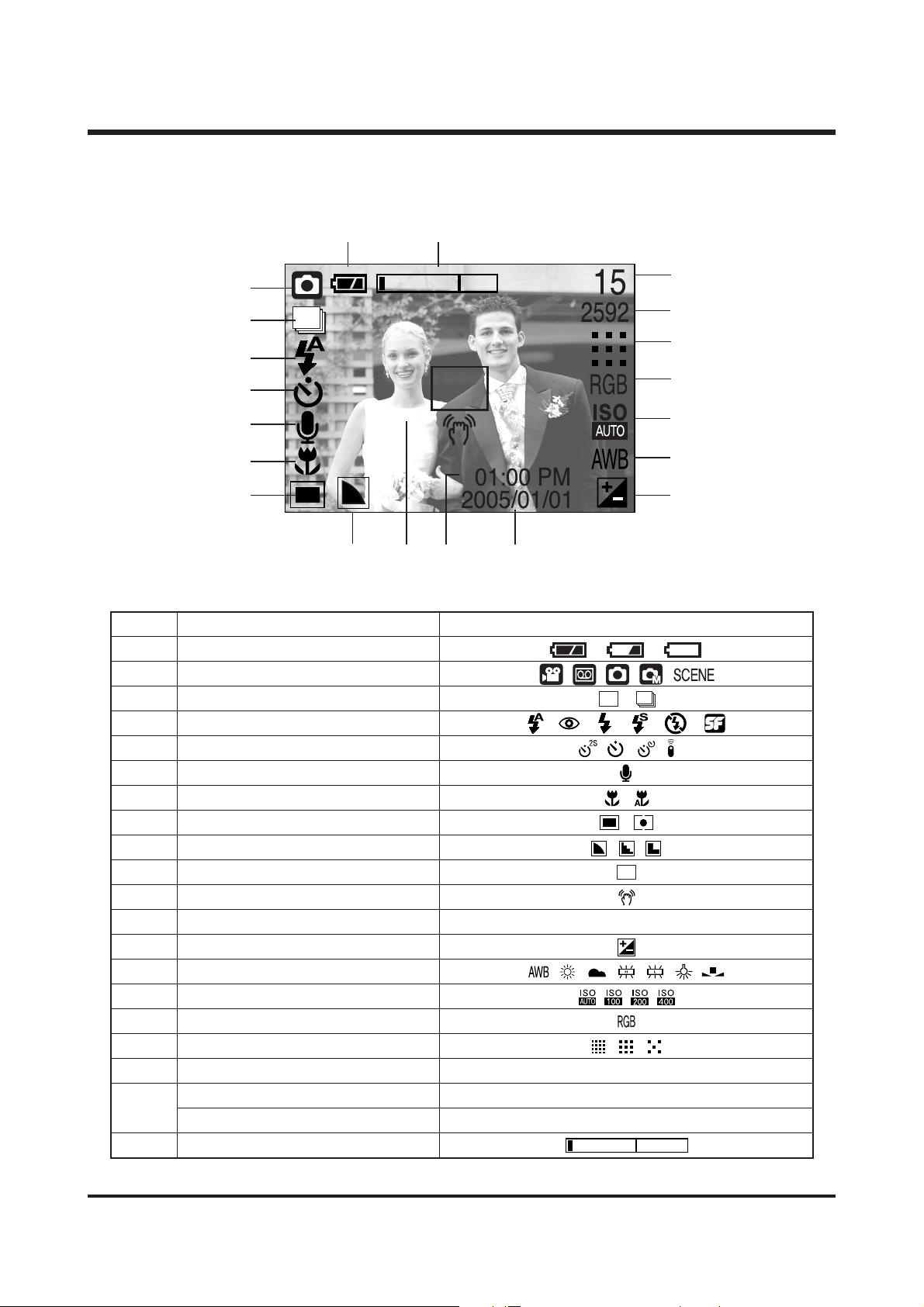
33.. LLCCDD mmoonniittoorr iinnddiiccaattoorr
■ Recording mode
No. Description Icons
1 Battery
2 Recording mode
3 Continuous shot
4 Flash
5 Self-timer
6 Voice memo
7 Macro
8 Metering
9 Sharpness
10 Auto focus frame
11 Camera shake warning
12 Date/ Time 2005/01/01 01:00 PM
13 Exposure compensation
14 White Balance
15 ISO
16 RGB
17 Image quality
18 Image size
2592, 2272, 2048, 1600, 1024, 640
Number of available shots remaining
15
Remaining time( Movie clip/ Voice recording)
00:01:30/ 01:00:00
20 Optical/Digital Zoom bar
[ Image & Full Status ]
②
⒃
③
④
⑤
⑥
⑮
⑭
⑬
⑫
⑪
⑩
⑦
⑧
⑨
⒔
⒕
①
⒗
⒖
19
Page 6

7
Ⅰ. SPECIFICATION
■ Play mode
No. Description Icons
1 Battery
2 Play mode
3 File type
4 Voice memo
5 Protect indicator
6 DPOF indicator
7 Stored image number 9
②
SIZE : 2592x1944 Image size
AV : F2.8 Aperture value
TV : 1/60 Shutter speed
ISO : 100 ISO sensitivity
FLASH : OFF Whether or not the
flash is used.
DATE : 2005/01/01 Recording date
⑥
③
④
⑤
⑦
①
Size : 2592X1944
Av : F2.8
Tv : 1/60
ISO : 100
Flash : Off
Date : 2005/01/01
Page 7
8
Ⅰ. SPECIFICATION
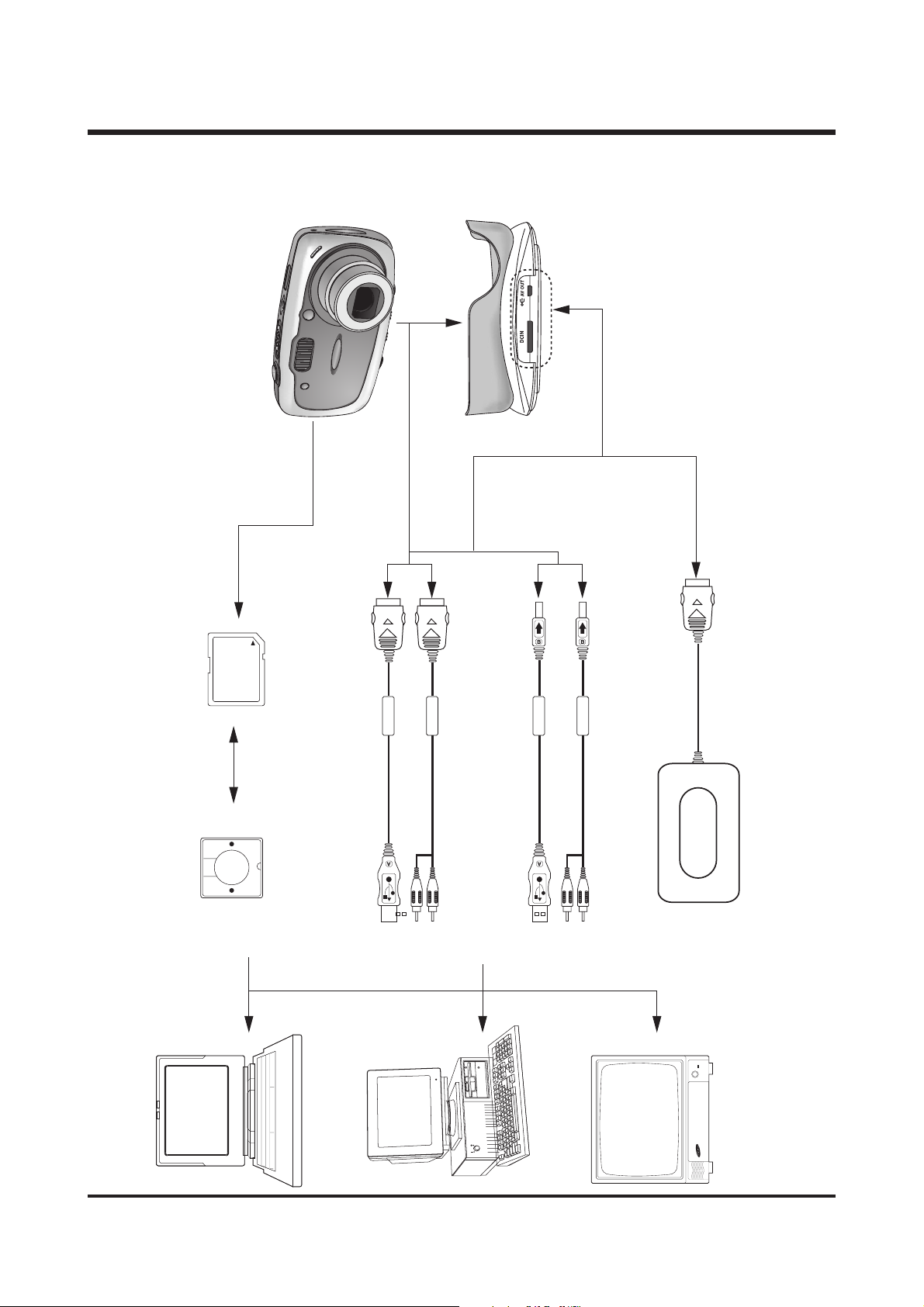
44.. CCoonnnneecctt iioo nn ddiiaaggrraamm
Cradle
SD Card
Card Reader
Lap top
USB Cable
AV Cable
USB Cable
IBM / MAC
AC Adaptor
AV Cable
TV Monitor
Page 8
9
Ⅰ. SPECIFICATION
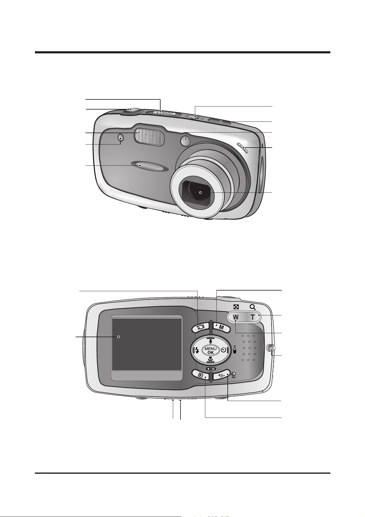
55..
IIddeennttiiffiiccaatt iioo nn ooff ffeeaattuurreess
Flash
Remote control
sensor
Lens
Power button
Auto Focus lamp
Speaker
Microphone
Shutter button
Mode switch
Function lamp
&
Self-timer lamp
LCD
monitor
LCD button
Strap eyelet
Zoom T button
(Digital zoom)
Zoom W button
(Thumbnail)
Play mode
button
Tripod socket
DC/USB/AV
connection terminal/
Cradle connector
+/-, DELETE
button
M button
(Album button)
Page 9
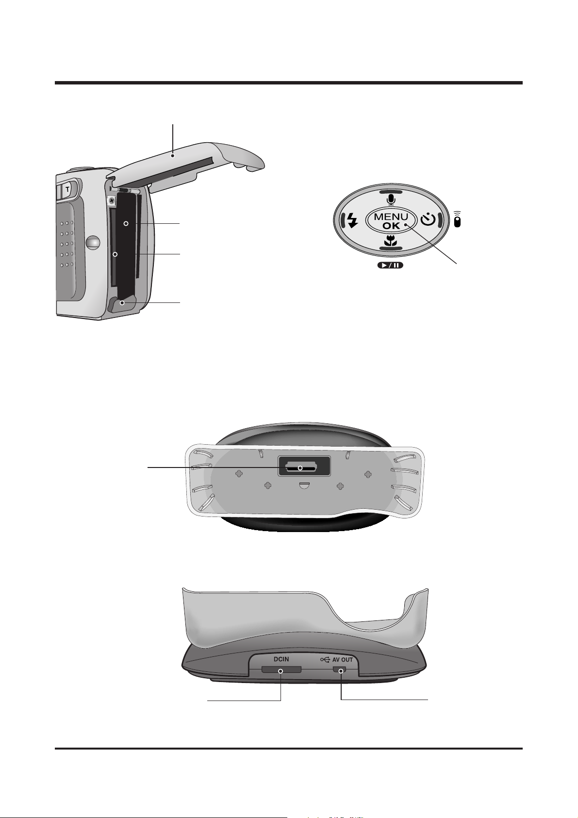
10
Ⅰ. SPECIFICATION
Battery holder
Memory card slot
Battery chamber
Battery chamber cover
FLASH/
LEFT button
MENU/ OK
button
Macro / DOWN button
Play & Pause button
SELF-TIMER/
REMOTE/
RIGHT button
Voice memo/ UP button
● Back
● Top
Camera connection
terminal
USB port
AV connection
terminal
DC input connection
point
Page 10

11
11.. IInnssttrruuccttiioonn ffoorr tthhee bbuunnddlleedd ssooffttwwaarreess ooff tthhee DDiiggiimmaaxx UU--CCAA 55
▶ USB Storage Driver
U-CA 5 uses the USB Storage Driver as the camera driver. You can use the camera as a USB card
reader.
After installing the driver and connecting this camera to the PC, you can download or view the
images
taken with U-CA5. A USB Storage Driver is provided only for Windows 98/98SE and a driver for
Macintosh is not included. But, you can use the camera with Mac 9.2 or later
▶ Xvid codec
This makes movie clips(MPEG-4) recorded with this camera play back on a PC.
To play back a movie clip recorded with this camera, you must install the XviD codec.
If a movie clip recorded with this camera does not play well, install this codec.
This software is only compatible with Windows.
If a move clip can't play back on the Mac OS, please visit the following site.
http://www.divx.com/divx/mac
▶ Digimax Viewer 2.1
Digimax Viewer 2.1 is the same software as Digimax Viewer 2.0
This software is only compatible with Windows.
▶ Digimax Reader : Text recognition program
You can save an image file that was captured in the TEXT mode as a text file with this program.
This software is only compatible with Windows
▶ Arcsoft PhotoImpression : Image editing program
You can edit or store still images that you download from the camera.
This software is only compatible with Windows.
22.. SSYYSSTTEEMM RREEQQUUIIRREEMMEENNTTSS
▶ For Windows
Computer PC with processor better than MMX Pentium 266MHz or higher
(XP : Pentium Ⅱ 300MHz)
O/S MS Windows 98, 98SE, 2000, ME, XP
Memory Minimum 32MB RAM (XP : 128MB)
Etc. USB port, XviD Codec
▶ For Macintosh
Computer PowerMac G3, G4, G4 Cube, iMac, PowerBook G3, G4, iBook series
OS Mac OS 9.2 or later
Memory Minimum 64MB
USB port, DivX Codec, QuickTime Player
ⅡⅡ.. IINNSSTTAALLLLAATTIIOONN && FFAAQQ
Page 11
12
Ⅱ. INSTALLATION & FAQ
33.. IInnssttaallllaattiioonn
▶ For Windows
Refer to the user manual for more information.
USB Storage Driver, Direct X, XviD Codec, Digimax Viewer 2.1, Digimax Reader, Arcsoft
PhotoImpression
▶ For Macintosh
A camera Driver, Viewer and Editing programs for Macintosh don't included on the application CD.
Connect the camera to the Macintosh and turn the camera power on. Mac will recognise the
camera directly.
To play back a movie clip on Mac, you have to install the DivX code.
44.. FFAAQQ
Using a Hand-made PC or a PC and OS that has not been guaranteed by the manufacturer is not
covered by the Samsung warranty.
▶▶ II nnss tt aall ll aa tt iioo nn
Q1. Though the Driver CD inserted in CD-ROM Drive, Auto Installation screen is not operate.
How can I install the program?
A1. First, It might be occurred if [Auto insert notification], the option to run Auto installation Screen
when the CD inserted was not set.
Set 「Auto insert notification」as follows.
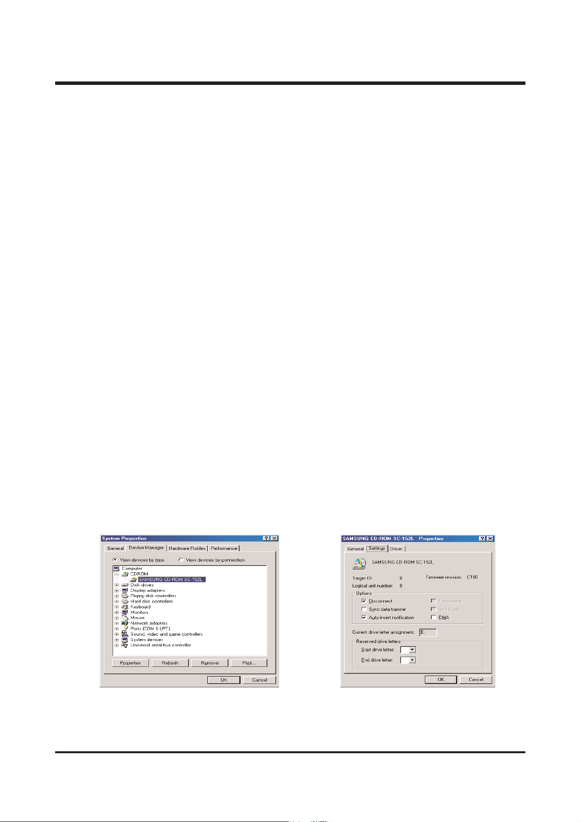
If selecting 「Start → Setting → Controller → System → Device Manager → CDROM」(see Fig. 1),
the installed CD-ROM appears. Double click this and then select the setting, the following
frame(see Fig. 2) will be shown.
Select 「Auto insert notification」from the options and reboot the PC.
< Fig. 1 > < Fig. 2 >
Page 12

13
Ⅱ. INSTALLATION & FAQ
Second, You need 5~10 seconds for running the automatic setup program according to the
capaility of select 「Samsung.exe」in the CD-ROM drive root directory.
Third, Without running the Auto Installation Screen, run the 「Windows Explorer」and install
the S/W directly at the desired program folder of CD-ROM root directory.
- USB Storage Driver : Run 「USB Driver」in the 「Setup.exe」folder.
- DirectX : Run 「USB Driver → DriectX8.1」in the 「DXSETUP.exe」folder.
- XviD Codec : Run 「XviD」in the 「XviD-1.0.2.exe」folder.
- Digimax Viewer 2.1 : Run 「Digimax Viewer 2.1」in the 「Setup.exe」folder.
- Digimax Reader : Run 「Digimax Reader → Kor → Install」in the 「Setup.exe」실행 folder.
- Arcsoft PhotoImpression 4 : Run 「PhotoImpression 4」in the 「Setup.exe」folder.
Q2. When the Digimax U-CA 5 Driver, DirectX are installed?
A2. After clicking the [Install] button, the camera driver is installed and DirecX 8.1 is installed.
In Windows 98/98SE/ME, DirectX is installed automatically.
In Windows 2000/XP, the computer checks the version of DirectX and install the DirextX when
the version of installed DirectX is older than that, or the DirectX is not installed.
Q3. Does the DirectX have to be installed?
A3. To play back a movie clip recorded with U-CA 5 on a PC, the DirectX and XviD codec
(commented later) must be installed.
DirectX is an application program interface (API) for creating and managing graphic images and
multimedia effects in applications such as games or active Web pages that will run in Microsoft's
Windows operating systems. As an API (using 2D or 3D graphics, sounds and videos) accesses a
hardware device directly, it was named "DirectX".
Page 13
14
Ⅱ. INSTALLATION & FAQ
Q5. What is XviD Codec and does it must be installed?
A5. Codec stands for Coder/Decoder. Basically it is a piece of software or a driver that adds a
support for certain video/audio format for your operation system. With codec, your system
recognizes the format the codec is built for and allows you to play the audio/video file
(=decode) or in some cases, to change another audio/video file into that format (=(en)code).
DivX codec is based on MPEG codec. It has high compression rate and it is good for
transmitting data.
As mentioned before, to play back a videos coded with DivX codec, the DivX codec must be
installed on a PC.
Though the MPEG-4 codec is installed, AVI type videos(coded by
DivX MPEG 4 - DVD to AVI) may not play back on a PC. In this case, install the DivX codec.
To play back a movie clip recorded with U-CA 5, we use XviD codec.
DivX becomes addware from version 5.xxx as it have advertisement. To resist the DivX
advertisement, the Xvid was released. XviD has lower image quality than DivX and Xvid can't
control the brightness of the video.
You must install the Xvid codec to play back a movie clip recorded with U-CA 5, the movie clip
information is as follow.
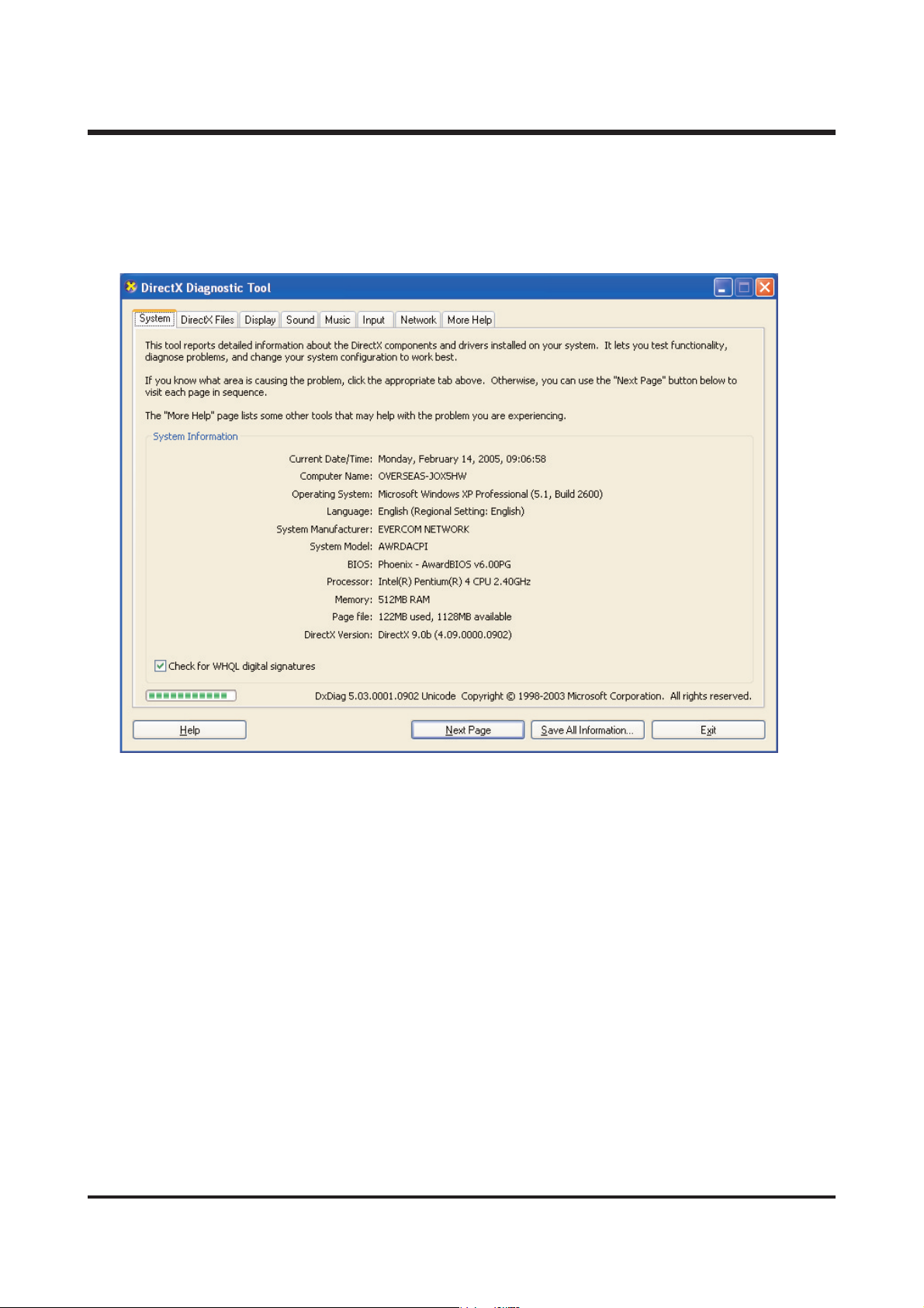
Q4. How do I check the version of DirectX?
A4. Select the [Start → Run]. type "dxdiag" on the text field, and click the [OK] button.
DirectX diagnostic tool window will display and you can check the version of the DirectX
(written bottom center of the window).
Page 14

15
Ⅱ. INSTALLATION & FAQ
< Trouble shooting 1 : Codec related problem>
As there are too many codecs and video formats, it is hard to select a proper codec for your PC.
And if different kinds of codecs are installed together, there may be a code corruptions and video file
can't play back. In this case, remove all of the codecs and install Xvid codec included in the S/W CD.
< Trouble shooting 1 : Graphic card related problem>
Though the Xvid codec is installed correctly, the video may not play back because of the graphic card.
In this case, update the graphic card driver by visiting the manufacturer's web-site.
The following driver will display on the [Sound & Multimedia] menu in the [Settings → Control panel]
Q6. How can I check whether the XviD codec install correctly or not?
A6. If the Xvid codec install correctly, you can view [XviD] folder by selecting
[Start → Program → XviD]..
Page 15
16
Ⅱ. INSTALLATION & FAQ
▶▶ UUssiinngg DDiiggiimmaaxx VViieewweerr 22..11
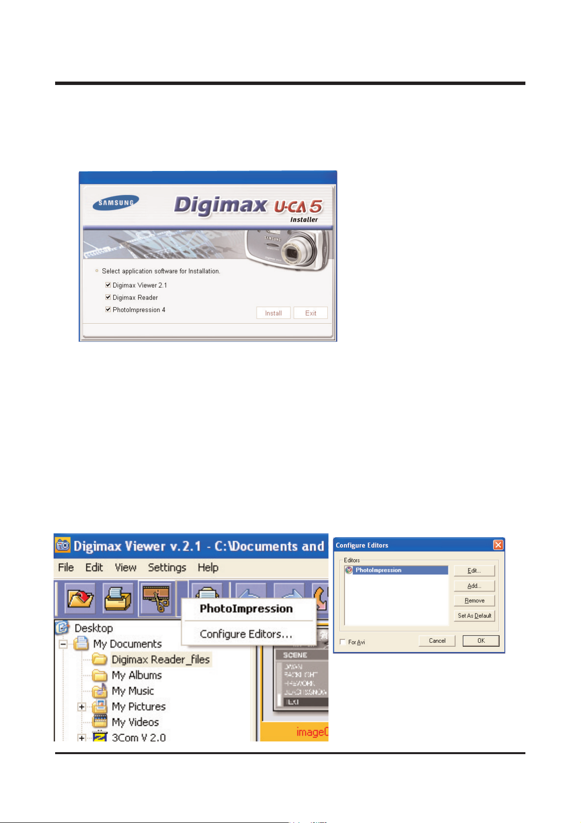
Q1. How can I register different editing program?
A1. Select an image and press the go to editing program icon. Click the [Configure Editors] menu.
A window for selecting a editing program will display.
- Edit : Rename the editing program
- Add : Adding a different program
- Remove : Remove a editing program
- Set As Default : Setting the selected program as a default editing program. It will run
automatically by clicking [Editor programs] menu.
- For Avi : For setting up the video editing program
Q7. Can I install Digimax Viewer2.1 or PhotoImpression 4 only?
A7. Select a application program you want on the program selection window displayed during setting
up the application software. You can view the brief explanation by moving the mouse point on a
program.
Page 16
17
Ⅱ. INSTALLATION & FAQ
Q2. A movie clip recorded with Digimax U-CA 5 can't play back..
A2. Digimax U-CA 5 uses XviD MPEG-4 codec.
To play back this file on a PC, XviD codec must be installed.
Install the XviD codec and play back the movie clip.
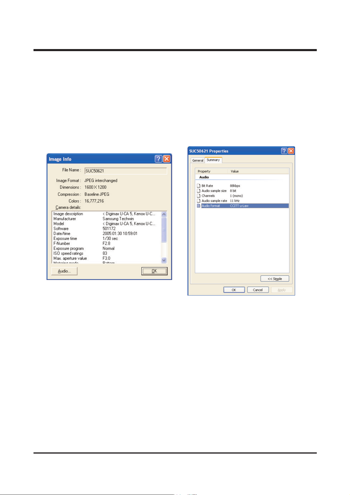
Q3. How can I view the voice memo(attached to an image)
information?
A3. Select an image and press the right mouse button.
Click the [Properties] button and you can view the image information.
If you select a voice memo file, you can view the voice memo file information.
<<<< FFoorr MMaaccii nnttooss hh >>>>
- When you buy the Macintosh, check the MacOS whether it is 9.2 or later and whether the
USB Mass Storage Support 1.3.5 is installed or not.
- If the version of Mac OS and USB Mass Storage Support can't be matched with our system
requirements, we don't hold any responsibility.
Q1. A movie clip recorded with U-CA5 can't play back on a macintosh.
A1. A codec for playing back the movie clip doesn't be installed.
Install the DivX codec for Mac as following steps.
1) Visit the following site for downloading the codec.http://www.divx.com/divx/mac
2) Click the [Free Download] button located upper right side of the page and a window for
downloading the DivX codec will display.
3) Select Mac OS you use and click the [Download] button. Save it on a folder you want to.
4) Run the downloaded file and the codec for playing back the movie clip will be installed.
For Mac OS X user, use Mplayer(http://mplayerosx.sourceforge.net) or VLC media player
(http://www.videolan.org/vlc/) to play back the movie clip.
Page 17

18
Ⅱ. INSTALLATION & FAQ
▶ The camera driver for Windows 98/98SE consists of the following 3 files.
1. U_CA5.inf
When U-CA5 is connected to a PC, this file induces USB Mass Storage installation.
2. U_CA5PDR.pdr
This is I/O related file. When you read/write/copy/delete the image on the Windows Explorer,
this file will activate.
3. U_CA5.sys
When a PC recognise the camera as a USB device, this file will activate.
▶ Checking whether the USB Storage driver is installed correctly or not.
After installing the USB Mass Storage for Windows 98/98SE, connect the camera and PC with
supplied USB cable and turn on the camera and PC.
The removable Disk will display.
For your information, Windows ME/2000/XP user need not install the USB Mass Storage Driver.
(1) The removable Disk will display.
(2) "The device is working properly." message will display on the system information window.
< Win 98/98SE >
- Disk drive : Samsung Digital Camera
- Harddisk controller : Samsung Digital Camera / USB Mass Storage Device
< Win ME >
- Disk drive: Samsung Digital Camera
- Universal Serial Bus(USB) controller : USB Mass Storage device
- Storage device : USB disk
< Win 2K/XP >
- Disk drive : Samsung Digital Camera USB Device
- Universal Serial Bus(USB) controller : USB Mass Storage device
- Storage volume : Normal
(3) The camera driver file has to be installed under the following folders.
< Windows 98 / 98SE >
U_CA5.inf : Windows/inf
U_CA5PDR.pdr : Windows/system/iosubsys
U_CA5.sys : Windows/system32/drivers
< Windows ME / 2000 / XP >
usbstor.sys : Windows/system32/drivers
usbstor.inf : Windows/inf
Page 18

19
Ⅱ. INSTALLATION & FAQ
▶▶ RReemmoovv ii nngg tthhee UUSSBB MMaassss SSttoorraaggee ddrriivveerr ffoorr WW ii nnddoowwss 9988//9988SSEE
When you remove the USB driver files for Windows 98/98SE manually, refer to the following steps.
1. Click the [Start] button.
2. Click the [실행] menus and type "regedit" to run the regedit program.
3. Select "HKEY_LOCAL_MACHINE\Enum\U_CA5" folder and press the DEL button to delete it.
4. Select "HKEY_LOCAL_MACHINE\Enum\SCSI\SAMSUNG_DIGITAL_CAMERA__" and delete the
VID:0839, PID:1032 folders by pressing the DEL button.
5. Select "HKEY_LOCAL_MACHINE\Enum\USB" folder and delete VID_0839&PID_1032 folder
by pressing the DEL button.
6. Select "HKEY_LOCAL_MACHINE\Enum\\System\CurrentControlSet\Services\Class\hdc" folder.
Select each folders related with U_CA5~ and delete them by pressing the DEL button.
7. Delete the following files located on the marked folders.
U_CA5.inf : Windows/inf/other
U_CA5PDR.pdr : Windows/system/iosubsys
U_CA5.sys : Windows/system32/drivers
If you are Windows 2000/XP user, do not delete the folders and files by using "regedit" program.
▶▶ CCoo ppyy aann iimm aaggee ffiillee ffrroomm tthhee ccaa mm eerraa ttoo aa PPCC,, tt hhee ff ii ll ee ccaann '' tt bb ee ccooppiieedd ..
During the file tramsmission, you operate the camera.
The icon located upper left side of the LCD monitor will blink, when a file is transferred (copy or
deletion) between the PC and the camera. Do not remove the USB cable until the icon stops
blinking To remove the USB cable in Windows 2000/ME/XP, use the [Unplug or Eject Hardware]
icon on the task bar.
☞ Don't operate the camera when the function lamp is blinking as this may cause damage to
data in the memory card.
Don't Operate the camera until the camera status lamp stops blinking.
You should allow 3~4 seconds before operating the camera.
Page 19
20
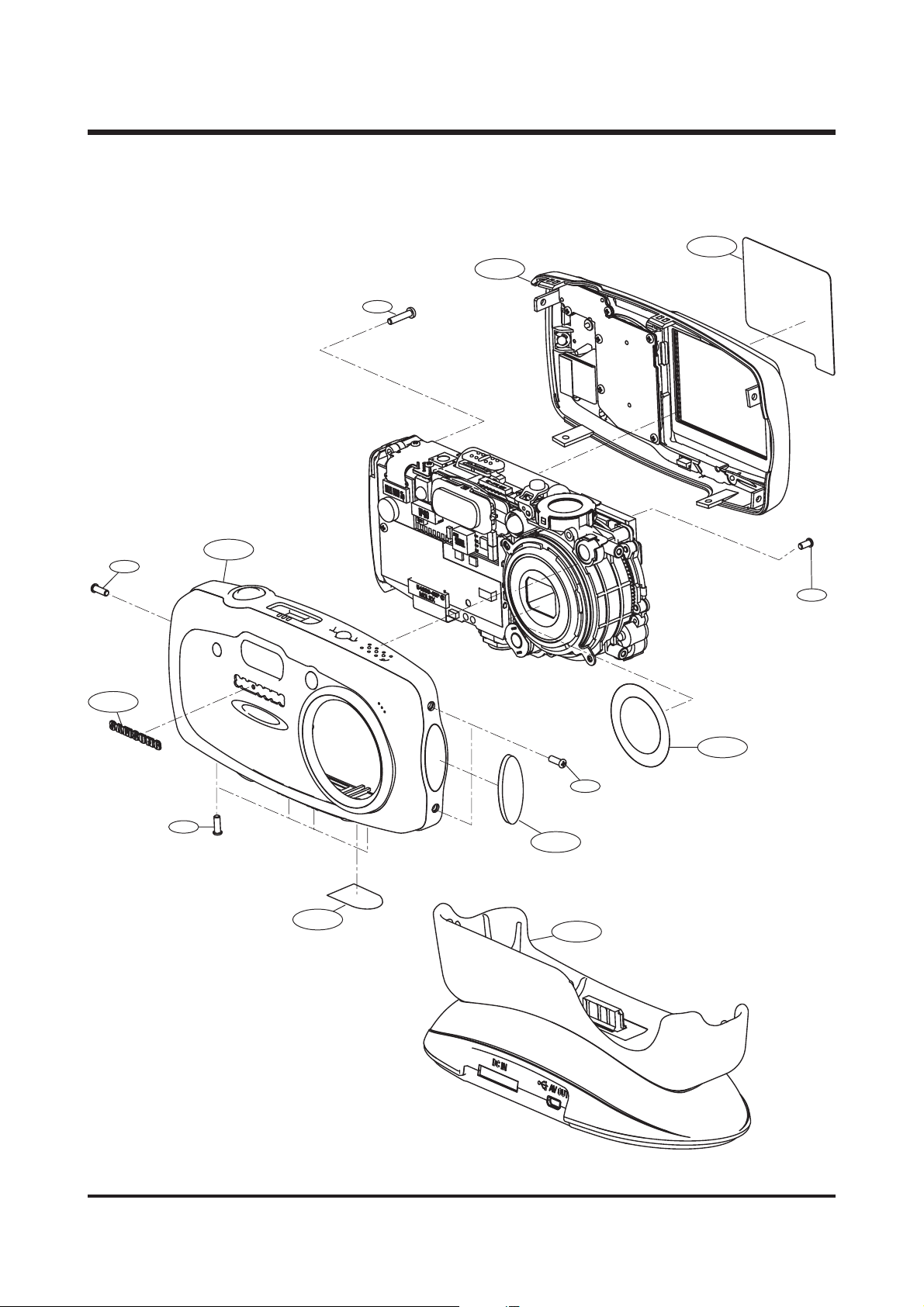
ⅢⅢ.. EEXXPPLLOODDEEDD VVIIEEWWSS AANNDD PPAARRTTSS LLIISSTT
1. MAIN ASSEMBLY
1-2
1-11
1-4
1-6
1-10
1-9
1-1
1-8
1-9
1-7
1-9
1-5
1-3
Page 20

21
Ⅲ. EXPLODED VIEWS AND PARTS LIST
▶▶
PARTS LIST
Fig.No. Parts No. Parts Name Q'ty Remarks
1-1 Q9007223801A FRONT COVER ASSY-KENOX U-CA 5 1 NEO GRAY
Q9007224301A FRONT COVER ASSY-KENOX U-CA 50 1 NEO BLUE
Q9007224001A FRONT COVER ASSY-KENOX U-CA 5 1 NEO WINE
Q9007221201A FRONT COVER ASSY-DIGIMAX U-CA 5 1 NEO GRAY
Q9007224801A FRONT COVER ASSY-DIGIMAX U-CA 5 1 NEO BLUE
Q9007224601A FRONT COVER ASSY-DIGIMAX U-CA 5 1 NEO WINE
1-2 Q9007221301A BACK COVER ASSY 1 NEO GRAY
Q9007224501A BACK COVER ASSY 1 NEO BLUE
Q9007224201A BACK COVER ASSY 1 NEO WINE
1-3 Q9010050101A CRADLE ASS'Y 1
1-4 Q7409178901A LCD SHIELD FOAM 1
1-5 Q7217328201A SIDE DECO 1
1-6 Q7017037701C LOGO PLATE 1
1-7 Q7012076401B DECORATION RING 1
1-8 Q7409178601A MIC LABEL_KENOX UCA 5_KOR (MIC) 1
Q7409178701A FCC LABEL_DIGIMAX UCA 5_EXP (MIC) 1
Q7409178201A FCC LABEL_DIGIMAX UCA 5_EXP (MBS) 1
Q7409179101A FCC LABEL_DIGIMAX UCA 5_EXP (MIK) 1
1-9 Q6003024201A SCREW 6
1-10 Q9761174507 SCREW 2
1-11 Q6003046201A SCREW 1
Page 21
22
Ⅲ. EXPLODED VIEWS AND PARTS LIST
2. BODY ASSEMBLY
2-27
2-39
2-39
2-
2-29
2-35
2-30
2-37
2-34
2-33
2-28
2-32
2-39
2-39
2-18
2-36
2-31
2-20
2-19
2-35
2-21
2-15
2-40
2-16
2-17
2-26
2-41
2-12
2-13
2-39
2-38
2-24
2-14
2-23
2-22
2-3
2-2
2-11
2-25
2-4
2-9
2-6
2-
2-1
2-8
2-10
2-7
2-5
Page 22

23
Ⅲ. EXPLODED VIEWS AND PARTS LIST
▶▶
PARTS LIST
Fig.No. Parts No. Parts Name Q'ty Remarks
2-1 Q7011049101A LCD FRAME 1
2-2 Q0704010501A LCD 1
2-3 Q7211068701A TRIPOD CONNECTOR 1
2-4 Q0961900301A SCREW 2
2-5 Q9002133501A BARREL ASSY 1
2-6 Q9765143007 SCREW 4
2-7 Q2904002102A IR CUT FILTER 1
2-8 Q7309043101A OLPF CUSHION 1
2-9 Q9761173507 SCREW 2
2-10 Q9001102001A CCD FPCB ASSY 1
2-11 Q4101032101A ESD SHEET 1
2-12 Q7011051001A BATTERY CONTACT 3
2-13 Q6107054601A BATTERY SPRING 1
2-14 Q7211074901A BATTERY CHAMBER_A 1
2-15 Q7211075201A BATTERY LOCK 1
2-16 Q6107059601A BATTERY LOCK SPRING 2
2-17 Q7411118301A BATTERY HINGE 1
2-18 Q7011048801A BATTERY PLATE 1
2-19 Q7011048901A BATTERY PLATE HOLDER 1
2-20 Q6107054501A BATTERY HINGE SPRING 1
2-21 Q7411118301A BATTERY HINGE 1
2-22 Q0601004601A AF LED 1
2-23 Q4101031701A AF LED FPCB 1
2-24 Q9008081301A MAIN PCB ASSY 1
2-25 Q4101030301A CONNECTOR FPCB 1
2-26 Q9008081501A POWER PCB ASSY 1
2-27 Q9008081701A TOP FPCB ASSY 1
2-28 Q2401008301A MAIN CONDENSOR 1
2-29 Q9001101901A REFLECTOR ASSY 1
2-30 Q7214087301A FRESNEL LENS 1
2-31 Q7214087201A REFLECTOR HOLDER 1
2-32 Q7014004101A REFLECTOR 1
2-33 Q7014004601A TRIG CONTACT 1
2-34 Q0611003101A XE-TUBE 1
2-35 Q7309039701A TUBE RUBBER 2
2-36 Q9008081901A STROBO PCB SMD ASSY 1
2-37 Q7211074801A BATTERY COVER 1 NEO GRAY
Q7211080601A BATTERY COVER 1 NEO BLUE
Q7211080901A BATTERY COVER 1 NEO WINE
2-38 Q4101033201A EMI SHEET 1
2-39 Q0961900301A SCREW 6
2-40 Q6003027501A SCREW 1
2-41 Q7211075001A BATTERY CHAMBER_B 1
Page 23

24
Ⅲ. EXPLODED VIEWS AND PARTS LIST
3. BARREL ASSEMBLY
3-36
3-20
3-35
3-30
3-34
3-1
3-31
3-37
3-3
3-2
3-10
3- 23
3-22
3-4
3-28
3-26
3-25
3-55
3-27
3-24
3-5
3-11
3-20
3-12
3-6
3-18
3-53
3-7
3-38
3-22
3-19
3-15
3-17
3-16
3-13
3-8
3-14
3-54
3-44
3-42
3-46
3-9
3-41
3-21
3-40
3-45
3-48
3-51
3-49
3-52
3-39
3-47
3-56
3-50
Page 24

25
Ⅲ. EXPLODED VIEWS AND PARTS LIST
▶▶
PARTS LIST
Fig.No. Parts No. Parts Name Q'ty Remarks
3-1 Q9002135901A LENS BASE ASS'Y 1
3-2 Q7212184003A LENS BASE 1
3-3 Q7411097601A AF GUIDER BAR_A 1
3-4 Q7411097701A AF GUIDER BAR_B 1
3-5 Q7411085902A ZOOM GEAR_A SHAFT 1
3-6 Q7411097801A ZOOM GEAR_B SHAFT 4
3-7 Q7411090001B ZOOM GEAR_C SHAFT 2
3-8 Q7411097901B ZOOM GEAR_D SHAFT 1
3-9 Q3107001701A ZOOM MOTOR 1
3-10 Q9611142007 SCREW 2
3-11 Q7212160001B ZOOM MOTOR GEAR 1
3-12 Q7212160101A ZOOM GEAR_A 1
3-13 Q7411085802A ZOOM GEAR_D 1
3-14 Q7411085702A ZOOM GEAR_C 1
3-15 Q7411085601B ZOOM GEAR_B 1
3-16 Q7212160602B ZOOM GEAR_E 2
3-17 Q7212172701A ZOOM GEAR_H 3
3-18 Q7212173801A ZOOM GEAR_G 1
3-19 Q7212172601A ZOOM COVER 1
3-20 Q7012075904A ZOOM COVER_B 1
3-21 Q6003040401A SCREW 2
3-22 Q0961900301A SCREW 1
3-23 Q9008062101A MAIN FPCB ASS'Y 1
3-24 Q4101025801A MAIN F PCB 1
3-25 Q9002104301A AF MOTOR ASS'Y 1
3-26 Q4101026701A ZOOM MOTOR FPCB 1
3-27 Q0608001001A PHOTO INTERRUPTER 2
3-28 Q0608000701A PHOTO REFLECTOR 1
3-29 Q7012069301A AF CLIP 1
3-30 Q9002129801A 3rd LENS BARREL ASS'Y 1
3-31 Q9002128901A 3rd LENS ASS'Y 1
3-32 Q7012079101A AF CLIP HOLDER 1
3-33 Q6001014001A SCREW 1
3-34 Q6107048305A 3RD LENS BARREL SPRING 1
3-35 Q7212181401A AF GUIDE HOLDER 1
3-36 Q0961900101A SCREW 1
3-37 Q0994913101A SCREW 1
3-38 Q6003040401A SCREW 2
3-39 Q7212180803A GUIDE PLATE 1
3-40 Q9002129001A 2nd LENS BARREL ASS'Y 1
3-41 Q9002128801A 2nd LENS ASS'Y 1
3-42 Q9005017101A SHUTTER ASS'Y 1
3-43 Q0961900301A SCREW 2
3-44 Q7409155801A SHUTTER SHIELD 1
3-45 Q7411106802A 2ND MOVE PIN 3
3-46 Q7012075703A F_PCB GUIDER 1
3-47 Q7212180702A ZOOM RING 1
3-48 Q7409138001A FRONT SHIELD 1
3-49 Q7012079001A 1ST PUSH PLATE 1
3-50 Q7411106702A 1ST MOVE PIN 3
3-51 Q7212180901A CAM BARREL 1
3-52 Q7012081901A FINDER HOLDER 1
3-53 Q9002133301A OUTER GUIDE BARREL ASS'Y 1
3-54 Q7212181001A OUTER CAM BARREL 1
3-55 Q9761173007 SCREW 5
3-56 Q9002128702A 1st LENS ASS'Y 1
Page 25
26
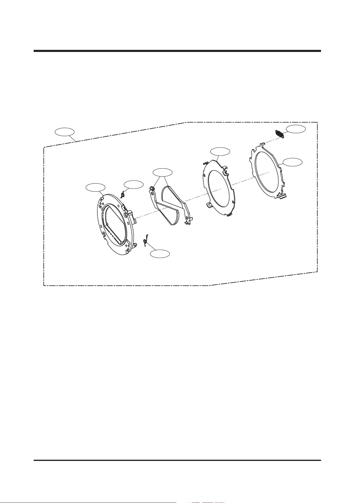
Ⅲ. EXPLODED VIEWS AND PARTS LIST
4. BARRIER ASSEMBLY
4-1
4-2
4-7
4-5
4-6
4-4
4-3
4-3
Page 26

27
Ⅲ. EXPLODED VIEWS AND PARTS LIST
▶▶
PARTS LIST
Fig.No. Parts No. Parts Name Q'ty Remarks
4-1 Q9002129401A BARRIER ASSY 1
4-2 Q7212181204A FRONT PANEL 1
4-3 Q6107053705A BARRIER CLOSE SPRING 2
4-4 Q7212181304A BARRIER_A 2
4-5 Q7012079406B BARRIER BASE 1
4-6 Q9002129501A BARRIER LEVER ASSY 1
4-7 Q6107052802A BARRIER OPEN SPRING 1
Page 27

28
Ⅲ. EXPLODED VIEWS AND PARTS LIST
5. FRONT COVER ASSEMBLY
5-3
5-6
5-4
5-5
5-1
5-2
Page 28

29
Ⅲ. EXPLODED VIEWS AND PARTS LIST
▶▶
PARTS LIST
Fig.No. Parts No. Parts Name Q'ty Remarks
5-1 Q7217327301A POWER BUTTON 1 NEO GRAY
Q7217347201A POWER BUTTON 1 NEO BLUE
Q7217350601A POWER BUTTON 1 NEO WINE
5-2 Q9007226701A FRONT COVER SUB ASSY-KENOX U-CA 5 1 NEO GRAY
Q9007226801A FRONT COVER SUB ASSY-KENOX U-CA 50 1 NEO BLUE
Q9007226901A FRONT COVER SUB ASSY-KENOX U-CA 5 1 NEO WINE
Q9007227001A FRONT COVER SUB ASSY-DIGIMAX U-CA 5 1 NEO GRAY
Q9007227101A FRONT COVER SUB ASSY-DIGIMAX U-CA 5 1 NEO BLUE
Q9007227201A FRONT COVER SUB ASSY-DIGIMAX U-CA 5 1 NEO WINE
5-3 Q7217327201A RELEASE BUTTON 1
5-4 Q7217328001A MODE SLIDE BUTTON 1 NEO GRAY
Q7217347001A MODE SLIDE BUTTON 1 NEO BLUE
Q7217350501A MODE SLIDE BUTTON 1 NEO WINE
5-5 Q7217328101A MODE SLIDE PLATE 1
5-6 Q6107059701A RELEASE SPRING 1
Page 29

Ⅲ. EXPLODED VIEWS AND PARTS LIST
6. BACK COVER ASSEMBLY
30
6-12
6-1
6-4
6-10
6-3
6-14
6-11
6-6
6-7
6-2
6-8
6-13
6-9
6-5
Page 30

31
Ⅲ. EXPLODED VIEWS AND PARTS LIST
▶▶
PARTS LIST
Fig.No. Parts No. Parts Name Q'ty Remarks
6-1 Q9007221501A KEY FPCB ASSY 1
6-2 Q9007227301A BACK COVER SUB ASSY 1 NEO GRAY
Q9007227401A BACK COVER SUB ASSY 1 NEO BLUE
Q9007227501A BACK COVER SUB ASSY 1 NEO WINE
6-3 Q7217327401A ZOOM BUTTON 1
6-4 Q7309043601A ZOOM RUBBER 1
6-5 Q7409170301A LCD SPONGE 1
6-6 Q7217327601A FUNCTION BUTTON-A 1
Q7217347701A FUNCTION BUTTON-A 1 NEO WINE
6-7 Q7217337301A FUNCTION BUTTON-B 1
Q7217347801A FUNCTION BUTTON-B 1 NEO WINE
6-8 Q7217337401A FUNCTION BUTTON-C 1
Q7217347901A FUNCTION BUTTON-C 1 NEO WINE
6-9 Q7217337501A FUNCTION BUTTON-D 1
Q7217348001A FUNCTION BUTTON-D 1 NEO WINE
6-10 Q7411115101A STRAP HOLDER 1
6-11 Q7017036201A E-RING 1
6-12 Q6003018401A SCREW 2
6-13 Q6003027501A SCREW 4
6-14 Q9007966801A NAVI BUTTON ASSY 1
Page 31

32
Ⅲ. EXPLODED VIEWS AND PARTS LIST
7. CRADLE ASSEMBLY
7-4
7-3
7-9
7-11
7-6
7-10
7-1
7-12
7-8
7-8
7-5
7-7
7-2
Page 32

33
Ⅲ. EXPLODED VIEWS AND PARTS LIST
▶▶
PARTS LIST
Fig.No. Parts No. Parts Name Q'ty Remarks
7-1 Q9008085101A SUB PCB ASSY-UC2(5M3 1
7-2 Q7309045701A CRADLE PAD 4
7-3 Q7209000403A CRADLE INT PCB HOLDE 1
7-4 Q9010050601A CRADLE BODY ASSY 1
7-5 Q7209000102A CRADLE BOTTOM 1
7-6 Q6003046901A CRADLE SCREW 2
7-7 Q6003046501A SCREW 4
7-8 Q6003046401A SCREW 4
7-9 Q9761174507 SCREW 2
7-10 Q4101032001A CRADLE FPCB 1
7-11 Q9008084901A CHARGER PCB SMD ASSY 1
7-12 Q9008085001A USB AV PCB SMD ASSY 1
Page 33

34
Ⅲ. EXPLODED VIEWS AND PARTS LIST
88 .. PP AA CC KKII NNGG II TT EEMMSS
8-4
8-15
8-17 8-6
8-18
8-19
8-20
8-22
8-7
8-16
CHARGE
8-21
8-11
8-12
8-1
8-3
8-8
8-10
8-9
8-5
8-13
8-2
8-14
Page 34

35
Ⅲ. EXPLODED VIEWS AND PARTS LIST
▶▶
PARTS LIST
Fig.No. Parts No. Parts Name Q'ty Remarks
8-1 QP960210101A PE BAG (FOR CAMERA)
8-2 Q6909011601A PE BAG (FOR ACCESSORY)
8-3 Q6901207801A INNER PAD
8-4 Q7409176501A STRAP
8-5 Q4609010301A DRIVER+VIEW+PHOTO IMPRE+VIDEO_IMPR+READER (KOR)
Q4609010401A DRIVER+VIEW+PHOTO IMPRE+VIDEO_IMPR+READER
8-6 Q4401000201A AC_ADAPTOR_4.2V
8-7 Q4301003201A LITHIUM-ION_SLB-1137
8-8 Q6904026201A POUCH_UCA 5_KOR/EXP
8-9 Q6806244601A Q/GUIDE_KENOX UCA 5_KOR
Q6806244701A Q/GUIDE_UCA 5_ENG
Q6806244801A Q/GUIDE_UCA 5_GER
Q6806244901A Q/GUIDE_UCA 5_FRA
Q6806245001A Q/GUIDE_UCA 5_SPA
Q6806245101A Q/GUIDE_UCA 5_ITA
Q6806245201A Q/GUIDE_UCA 5_CHI(T)
Q6806245301A Q/GUIDE_UCA 5_DUT
Q6806245401A Q/GUIDE_UCA 5_POR
Q6806245501A Q/GUIDE_UCA 5_SWE
Q6806245601A Q/GUIDE_UCA 5_DEN
Q6806245701A Q/GUIDE_UCA 5_FIN
Q6806245801A Q/GUIDE_UCA 5_RUS
Q6806245901A Q/GUIDE_UCA 5_CHI(S)
Q6806246001A Q/GUIDE_UCA 5_TK
8-10 Q6806246101A U/MANUAL_KENOX UCA 5_KOR
Q6806246201A U/MANUAL_Digimax UCA 5_ENG
Q6806246301A U/MANUAL_Digimax UCA 5_GER
Q6806246401A U/MANUAL_Digimax UCA 5_FRA
Q6806246501A U/MANUAL_Digimax UCA 5_SPA
Q6806246601A U/MANUAL_Digimax UCA 5_ITA
Q6806246701A U/MANUAL_Digimax UCA 5_CHI(T)
Q6806246801A U/MANUAL_Digimax UCA 5_DUT
Q6806246901A U/MANUAL_Digimax UCA 5_POR
Q6806247001A U/MANUAL_Digimax UCA 5_SWE
Q6806247101A U/MANUAL_Digimax UCA 5_DEN
Q6806247201A U/MANUAL_Digimax UCA 5_FIN
Q6806247301A U/MANUAL_Digimax UCA 5_RUS
Q6806247401A U/MANUAL_Digimax UCA 5_CHI(S)
Q6806247501A U/MANUAL_Digimax UCA 5_TK
Page 35

36
Ⅲ. EXPLODED VIEWS AND PARTS LIST
Fig.No. Parts No. Parts Name Q'ty Remarks
8-11 Q6806247701A C/MANUAL_KENOX UCA 5_KOR
Q6806247801A C/MANUAL_Digimax UCA 5_ENG
Q6806247901A C/MANUAL_Digimax UCA 5_GER
Q6806248001A C/MANUAL_Digimax UCA 5_FRA
Q6806248101A C/MANUAL_Digimax UCA 5_SPA
Q6806248201A C/MANUAL_Digimax UCA 5_POR
Q6806248301A C/MANUAL_Digimax UCA 5_RUS
Q6806248401A C/MANUAL_Digimax UCA 5_CHI(T)
Q6806251301A C/MANUAL_Digimax UCA 5_CHI(S)
8-12 Q6807002601F WARRANTY CARD_KOREA
Q6807003003U WARRANTY CARD_EXP
Q6807010902B WARRANTY CARD_RUS
Q6807011301B WARRANTY CARD_TSOE(CHINA)
Q6807009502E CARD_PRODUCT(Mexico)
8-13 Q6901205901A G/T BOX_KENOX UCA 5_KOR
Q6901206001A G/T BOX_Digimax UCA 5_EXP/AUS
Q6901206101A G/T BOX_Digimax UCA 5_EXP/AUS_PREMIUM
Q6901206201A G/T BOX_Digimax UCA 5_USA/CAN
Q6901206301A G/T BOX_Digimax UCA 5_USA/CAN_PREMIUM
Q6901207701A G/T BOX_Digimax UCA 5_CHI(S)_TSOE
Q6901207901A G/T BOX_Digimax UCA 5_CHI(S)_TSOE_PREMIUM
8-14 Q6804068801A STICKER_G/T BOX_UCA 5_Blue
Q6804069001A STICKER_G/T BOX_Digimax UCA 5_EXP/AUS_Blue
Q6804069101A STICKER_G/T BOX_Digimax UCA 5_EXP/AUS_PREMIUM_Blue
Q6804069201A STICKER_G/T BOX_Digimax UCA 5_USA_BLUE
Q6804069301A STICKER_G/T BOX_Digimax UCA 5_USA_PREMIUM_BLUE
Q6804071801A STICKER_G/T BOX_Digimax UCA 5_CAN_PREMIUM_BLUE
Q6804072201A STICKER_G/T BOX_UCA 5_WINE
Q6804072401A STICKER_G/T BOX_Digimax UCA 5_EXP/AUS_WINE
Q6804072501A STICKER_G/T BOX_Digimax UCA 5_EXP/AUS_PREMIUM_WINE
Q6804072601A STICKER_G/T BOX_Digimax UCA 5_USA_WINE
Q6804072701A STICKER_G/T BOX_Digimax UCA 5_CAN_WINE
Q6804072801A STICKER_G/T BOX_Digimax UCA 5_USA_PREMIUM_WINE
Q6804072901A STICKER_G/T BOX_Digimax UCA 5_CAN_PREMIUM_WINE
8-15 Q9010050101A CRADLE
8-16 Q4309001601A SBC-L3
8-17 Q3801003001A AC CODE CABLE_KOR
Q3801003201A AC CODE CABLE_EXP
Q3801003101A AC CODE CABLE_USA
Q3801001001A AC CODE CABLE_UK
Q3801003401B AC CODE CABLE_AUS
Q3801003701A AC CODE CABLE_CHI
8-18 Q3802002801A USB CABLE
8-19 Q3802003501A 24PIN USB CABLE
8-20 Q3802002901A VIDEO CABLE
8-21 Q3802003401A 24PIN AV CABLE
8-22 Q4602000601A SECURE DIGITAL CARD(32MB)
Q4602000701A SECURE DIGITAL CARD(64MB)
Q4602001301A SECURE DIGITAL CARD(128MB)
Q4602001901A SECURE DIGITAL CARD(256MB)
Page 36

37
Ⅲ. EXPLODED VIEWS AND PARTS LIST
Symbol Parts No. Parts Name Q’ty Remarks
F2 Q3601000701A CHIP FUSE 1
Q14 Q0505002701A FETTKY(SSM6J50TU) 1
T1 Q2601001301A TRANSFORMER 1
BTP1 Q4304000101A BUTTON CELL BATTERY 1
U1 Q1009001401A PWMIC 1
9. ELEC. PARTS
1) POWER PCB ASSY(TOP)
▶▶
PARTS LIST
F2
T1
BTP1
Q14
U1
Page 37

38
Ⅲ. EXPLODED VIEWS AND PARTS LIST
Symbol Parts No. Parts Name Q’ty Remarks
Y2 Q2802002601A CRYSTAL(VT-200-F) 1
U4 Q1103001901A SERIAL EEPROM 1
J2 Q3719003901A CRADLE CONNECTOR 1
SLOT Q3708884501A SD CARD CONNECTOR 1
2) MAIN PCB ASSY(BOTTOM)
▶▶
PARTS LIST
Y2
U4
J2
SLOT
Page 38

39
Ⅲ. EXPLODED VIEWS AND PARTS LIST
Symbol Parts No. Parts Name Q’ty Remarks
S1 Q3403969201A RELEASE SWITCH 1
S2 Q3408001301A SLIDE SWITCH 1
S3 Q3409001901A TACT SWITCH 1
SENSOR Q1409000201A REMOCON RECWIVER 1
3) TOP F PCB ASSY
▶▶
PARTS LIST
S1
SENSOR
S3
S2
Page 39

40
Ⅲ. EXPLODED VIEWS AND PARTS LIST
Symbol Parts No. Parts Name Q’ty Remarks
T1 Q2601002501A TRANSFORMER 1
T2 Q2704002701A TRIG TRRABS 1
Q3 Q1407001201A IGBT 1
4) STROBO PCB ASSY
▶▶
PARTS LIST
T2
Q3
T1
Page 40

41
Ⅲ. EXPLODED VIEWS AND PARTS LIST
PAGE PARTS NO. PARTS NAME SPEC SYMBOL
20 Q9007223801A FRONT COVER ASSY-KENOX U-CA 5 NEO GRAY
20 Q9007224301A FRONT COVER ASSY-KENOX U-CA 5 NEO BLUE
20 Q9007224001A FRONT COVER ASSY-KENOX U-CA 5 NEO WINE
20 Q9007221201A FRONT COVER ASSY-DIGIMAX U-CA 5NEO GRAY
20 Q9007224801A FRONT COVER ASSY-DIGIMAX U-CA 5NEO BLUE
20 Q9007224601A FRONT COVER ASSY-DIGIMAX U-CA 5NEO WINE
20 Q9007221301A BACK COVER ASSY NEO GRAY
20 Q9007224501A BACK COVER ASSY NEO BLUE
20 Q9007224201A BACK COVER ASSY NEO WINE
20 Q9010050101A CRADLE ASS'Y
20 Q7217328201A SIDE DECO
20 Q7012076401B DECORATION RING
22 Q0704010501A LCD
22 Q9002133501A BARREL ASSY
22 Q9001102001A CCD FPCB ASSY
22 Q9008081301A MAIN PCB ASSY
22 Q4101030301A CONNECTOR FPCB
22 Q9008081501A POWER PCB ASSY
22 Q9008081701A TOP FPCB ASSY
22 Q9008081901A STROBO PCB SMD ASSY
22 Q7211074801A BATTERY COVER NEO GRAY
22 Q7211080601A BATTERY COVER NEO BLUE
22 Q7211080901A BATTERY COVER NEO WINE
28 Q73217327301A POWER BUTTON NEO GRAY
28 Q7217347201A POWER BUTTON NEO BLUE
28 Q7217350601A POWER BUTTON NEO WINE
34 Q3802002801A USB CABLE
34 Q3802003501A 24PIN USB CABLE
34 Q3802002901A VIDEO CABLE
34 Q3802003401A 24PIN AV CABLE
34 Q4401000201A AC_ADAPTOR_4.2V
37 Q3601000701A CHIP FUSE F2
37 Q0505002701A FETTKY SSM6J50TU Q14
37 Q2601001301A TRANSFORMER T1
37 Q4304000101A BUTTON CELL BATTERY BTP1
37 Q1009001401A PWMIC U1
38 Q2802002601A CRYSTAL VT-200-F Y 2
38 Q1103001901A SERIAL EEPROM U4
38 Q3719003901A CRADLE CONNECTOR J2
38 Q3708884501A SD CARD SLOT
39 Q3403969201A RELEASE SWITCH S1
39 Q3408001301A SLIDE SWITCH S2
39 Q3409001901A TACT SWITCH S3
39 Q1409000201A REMOCON RECEIVER SNESOR
40 Q2601002501A TRANSFORMER T1
40 Q2704002701A TRIG TRANS T2
40 Q1407001201A IGBT Q3
11 00 .. II NNIITTII AALL PPAARRTTSS LLIISSTT
Page 41

42
ⅣⅣ.. AADDJJUUSSTTMM EENNTT
11.. DDiiggiittaall ccaammeerraa sseerrvviiccee
To take a digital camera service(Repair, Tuning and Checking), the following equipments have to be
arranged.
The sequences for the camera service are as shown
alongside.
1. Receiving the camera
When receiving a camera, check whether the accessories
are included or not and ask the customer exact problems.
2. Checking the camera
Checking the camera with priority given to the exact
problems to find overall malfunctions.
3. Repairing the camera
Repair the camera malfunctions found at the step 2.
4. Inspection
After repairing the camera, inspect all of the camera
functions.(See p.52)
※ The illustrations may be different from the real display in accordance with the camera model.
11.. CChh eecckkiinngg tt hhee ccaammeerr aa
aa nn dd II nn ss ppee cctt iioo nn
22.. RReepp aaiirriinn gg tthhee ccaammeerr aa 33.. TTuunn ii nngg
Receiving the camera
Checking the camera
Repairing the camera
Tuning
Inspection
Finish
Page 42

43
Ⅳ. ADJUSTMENT
11)) EE qquuiippmmeenn ttss ffoorr cchheecc kk iinn gg aa nndd iinnssppee cc tt iioonn
To check and inspect the camera malfunction, the following equipments have to be arranged.
①①
②②
③③
⑤⑤
⑥⑥
⑦⑦
⑧⑧
⑪⑪
⑨⑨
⑩⑩
④④
No. Device Description
1 PC for inspection - Installing a digital camera driver or Checking the removable device
- Checking the file transference(upload and download)
- Playing back the still image or movie clip
2 HARD RACK, For the compatibility test.
by Operating System by the O/S(WIN 98SE, ME, 2000, XP)
3 Driver CD, by camera models S/W CDs for installing a camera driver
4 USB HUB For using all kinds of USB cable at a time
5 USB cable, by camera models For checking file transference(upload and download) by camera models
6 Chart for checking colors For checking color and image resolution before or after camera repair
7 TV MONITOR For checking video output and whether NTSC/PAL can be selected
8 Memory card by types For checking card recognition by brands and sizes
9 A/V CABLE For checking whether the image can be displayed on a external monitor
10 POWER SUPPLY For checking camera power by camera models
11 Power cable by camera models
Page 43

44
Ⅳ. ADJUSTMENT
22)) EE qquuiipp mmee nn tt ss ff oo rr ccaamm eerraa rreepp aaiirr
To repair the camera, the following equipments have to be arranged.
①①
②②
③③
⑤⑤
⑥⑥
⑪⑪
⑨⑨
④④
⑩⑩
⑧⑧
⑪⑪
⑫⑫
⑬⑬
⑦⑦
No. Device Description
1 A set of tools Pincette/ Screwdriver/ Discharger etc.
2 Cleaning paper For cleaning camera lens and camera parts
3 Detergent container For containing detergent
4 Parts case For keeping various camera parts and disassembled camera parts
5 Anti-electricity mat For repairing table made from anti-electricity material
6 Soldering sponge For removing solder
7 Air pump For removing various kinds of dust
8 LIGHT BOX Color temperature 5100
9 POWER SUPPLY 7.5V 2.0A
10 Soldering iron Soldering iron that can select temperature
11 Tester Portable tester that can test AC/DC, Ω,♪ ect.
12 BATTERY & AC ADAPTOR & Rechargeable battery by camera models
AC ADAPTOR - SBP3603/ SBP3605/ SBP3606
- SLB 1437
- SBP 1103
Page 44

45
Ⅳ. ADJUSTMENT
33)) EE qquuiipp mmee nntt ss ffoorr cc aammeerr aa ttuunn ii nngg
To tune the camera, the following equipments have to be arranged.
①①
②②
③③
⑤⑤
⑥⑥
No. Device Description
1 AE TESTER For tuning AE and STROBE
2 AWB LIGHT For checking and tuning AWB
SOURCE BOX
3 COLOR chart For checking AWB and color of images
4 AF chart For tuning AF
5 Chart for checking For checking image resolution
resolution
6 TRIPOD
④④
Page 45

46
Ⅳ. ADJUSTMENT
44)) CChh eecckk ll iisstt ffoorr DDiiggiittaall ccaammeerr aa rr eeppaaiirr
To check the digital camera functions before/after repairing, refer to the check list.
NNoo.. CChh eecckkiinngg iitteemm CChh ee cckk ppooii nntt
1 - Check the scratch, stain, misprint.
- Check whether the screws are turned firmly.
- Check the corrosion of terminal, bad exterior.
- Do chemical and glue test to the printing/ painting parts.
2 - Check the connecting and contact condition.
3 - Insert the batteries with the correct polarity and check the
contact condition.
- Check whether the cover is opened easily after closing.
4 - The card can be inserted or removed easily and cover is
closed firmly.
- Do inserting and removing card(SD/MMC) test two times.
→ The card must be inserted firmly and has not to spring out.
- Insert the card/batteries and give a little impact on the
camera. The camera must recognize the card and “CARD
LOCKED”message has not to be displayed.
5 - When the cable is inserted, check whether the images play
back on the external monitor.
6 - Check whether the green LED is blinking, SAMSUNG LOGO is
on and the start-up sound sounds.
- Check the “L”and “FINE”icon on the LCD monitor.
- Check whether the AE function is correct at the low light and
high light condition.
- Check whether the “beep”sounds on the recording and movie
clip mode.
→ The “beep”can be sounded in the microphone part. Check
that in a quiet room.
7 - Press the zoom W/T button with the viewfinder.
→ Check dust and percentage of the frame seen, zoom rate.
- Press the zoom W/T button with the TFT-LCD monitor.
→ Check the zoom rate and whether the zoom bar moves
smoothly.
8 - Check whether the Macro icon(Flower) is displayed on the
LCD monitor.
- Check the AF in the Macro focus with the TFT-LCD monitor.
9 - Check whether the subject captured from 2M has over or
under exposure and the fucus is clear.
Check the exterior of a camera.
Insert the adapter.
Check the battery cover.
Check the card condition after
inserting the card.
Insert the Video cable.
Turn on the camera.
Press the zoom W/T button.
Macro focus.
Normal focus.
Page 46

47
Ⅳ. ADJUSTMENT
NNoo.. CChh eecckk ii tteemm CChheecc kk ppoo ii nntt
10 - Check whether the icon and counter are displayed on the
LCD monitor.
11 - Check whether the recording time is displayed and there
are a noise, dim frame and discontinuous frame in the movie
clip.
12 - Check whether the zoom rate is changed and there are
unclear part, noise and dim part in the image.
- The distance from the subject is 2M and have to use the
FILL IN flash.
13 - Check whether the PLAY mode can be selected without any
problem and there are any noise, frame shaking and
discoutinuous frame.
- Check the voice recorded in the still image and the movie clip.
- Check whether the still image can be enlarged correctly
with the 5 function button.
14 - Select 2 sec. of slide show interval time and check whether
there are any noise, image shaking and discontinuous frame.
15 - Check whether the mode dial is rotated with the equal force.
- Check whether each camera mode can be recognized correctly.
16 - Check whether there are unclear part, dim part, noticeable
flare, noise, ghost image and smear.
17 - Check whether all images are deleted.
18 - Check whether the “NO IMAGE”message is displayed on the
LCD monitor.
- Check whether the LARGE, FINE icon and 0018 number are
displayed.
- Check whether the camera power is turned off without any
problem.
MANUAL focus.
Take a movie clip with
TELE zoom during 10 seconds.
Take a chart with TELE zoom
in a low light condition.
Play back a image with
the TFT LCD monitor.
Start the slide show
in the PLAY mode.
Try to rotate the mode dial.
Download a image from a PC
with USB cable and check the
image quality in a external
monitor.
Format the card in the PLAY
mode.(Delete all images in the
PLAY mode)
Check whether there is no image
and reset the camera. Remove
the card and turn off the camera.
Page 47

48
Ⅳ. ADJUSTMENT
22.. TTuunniinngg iitteemm bbyy cchhaannggeedd ppaarrttss
After changing the electronic parts of Digimax U-CA 5, the parts have to be tuned in accordance
with the tuned items. The items listed on the table are have to be tuned after changing.
11)) EE qquuiipp mmeenn ttss ffoorr ttuunn ii nngg
▶ Equipments
- AE TESTER : AE TESTER can test upto LV 15.7
- POWER SUPPLY : 7V/2A
▶ Chart
- Focus chart : Download “AFCHART.pdf”file from the Samsung camera Service site(www.ssa.net)
and print it.
22)) CChheecc kk ii nngg tthhee cc aammeerraa ff ii rrmm wwaa rree vv eerrssiioonn
1. Remove all kinds of card. 2. Use the AC adapter or fully charged
batteries.
PROCESS MAIN SUB BARREL CCD
CODE PCB PCB ASS’Y
FIRMWARE UPGRADE ● ●
CCD DEFECT CELL 6 ● ●
PUNT ADJ. 2 ● ● ●
SHUTTER CLOSE TIME ADJ. 7 ● ● ●
BACK LASH ADJ. 9 ● ● ●
FLASH ADJ. 13 ● ●
BATTERY LEVEL 5 ● ●
OB SETTING 15 ● ●
BURNING TEST 10 ● ● ● ●
EEPROM READ 16
EEPROM WRITE 17
Page 48

49
Ⅳ. ADJUSTMENT
3. Set the mode dail to VOICE RECORDING mode and turn on the camera.
4. Press the buttons as following order.
(Left button 3 times -> Right button 1time -> Down button 1time -> +/- button 1time)
5. After pressing the buttons as shown above, the firmware version will display on the LCD.
①① ②②
③③
④④
Page 49

50
Ⅳ. ADJUSTMENT
33)) UUppgg rraaddiinngg tthhee ff ii rr mm wwaarr ee
1. Insert the SD card that has the firmware file and set the mode dail to VOICE RECORDING
mode. Turn on the camera.
※※ WWhheenn yyoouu uuppddaattee tthhee ffiirrmmwwaarree,, yyoouu hhaavvee ttoo
uussee tthhee AACC aaddaappoorr oorr ffuullllyy cchhaarrggeedd bbaatttteerryy..
2. Press the buttons as following order.
(Left button 3 times -> Right button 1time -> Down button 1time -> +/- button 1time)
3. When press the buttons as above No. 2, the update is processed then remove the SD card.
4. After finishing update, you have to reset the camera in SET UP menu.
①① ②②
③③
④④
Page 50

51
Ⅳ. ADJUSTMENT
33.. AAddjjuussttmmeenntt
To tune all items, all kinds of code by items have to be inserted in program file and saved it to
the SD card as TXT file type. The codes are listed below.
<Description of TXT file>
If the program is saved as shown above, the file name has to be saved as UC2ADJ.TXT.
※ After inserting each code, [;] mark has to be inserted.
CCoodd eess ooff pprroo ggrraamm DDee sscc rrii ppttiioonn oo ff ccooddee ss
<1> PROCESS CODE ; Insert the PROCESS CODE that you want to tune
<2> 65535 ; 65535 --> DEFAULT
<3> PROCESS CODE ; Insert the PROCESS CODE that you want to tune.
<4> 0 OR 1 ; Insert 1 to write tuned codes to the EEPROM.
<5> 0 OR 1 ; To save the result data to the SD card, insert 1 or 0.
<6> CONDITION ; Insert each tuning item's condition.(See each tuning item)
<7> SPEC ; Insert each tuning item's condition.(See each tuning item)
<8> NOT Not used
<9> NOT Not used
<10> NOT Not used
<11> NOT Not used
<12> NOT Not used
<13> NOT Not used
<14> 0 0 --> DEFAULT
<15> 0 0 --> DEFAULT
Page 51

52
Ⅳ. ADJUSTMENT
11)) CCCCDD DD EEFFEECCTT CCEELLLL
After changing the MAIN PCB and CCD, tune the DEFECT CELL of CCD.
<Codes of program>
<How to tune the item>
a. Insert the codes and save the program in the SD card.
b. Insert the SD card to the camera.
c. Turn on the camera.
(Set the mode dial to Still image mode)
d. <Figure 1-1> will display on the TFT LCD monitor and the items will be tuned automatically.
e. After completing the tuning, the camera will be turned off.
※ If the tuning is incomplete, <Figure 1-2> will display. In this case, re-try the tuning process.
<Figure 1-1> <Figure 1-2>
BB AASSIICC PPRROO GGRRAAMM CCCCDD DDEEFFEE CCTT CCEE LLLL
<1> PROCESS CODE ; <1>6;
<2> 65535 ; <2>65535;
<3> PROCESS CODE ; <3>6,0;
<4> 0 OR 1 ; <4>1;
<5> 0 OR 1 ; <5>0;
<6> CONDITION ; <6>1,2000,0,6;
<7> SPEC ; <7>12000,0;
<8> NOT <8>;
<9> NOT <9>;
<10> NOT <10>;
<11> NOT <11>;
<12> NOT <12>;
<13> NOT <13>;
<14> 0 <14>0;
<15> 0 <15>0;
EXPOSURE : 1 sec
HOT LEVEL : 2452
EXPOSURE : 8 sec
REF LEVEL : 2000
DEFECT PIXEL : 6847
SUCCESS!
EXPOSURE : 1 sec
HOT LEVEL : 2452
EXPOSURE : 8 sec
REF LEVEL : 2000
DEFECT PIXEL : 6847
FAIL!
Page 52

53
Ⅳ. ADJUSTMENT
22)) PPUUNNTT AADDJJUUSSTTMMEENNTT
After changing the MAIN PCB and BARREL, tune the PUNT.
<Codes of program>
<How to tune the item>
a. Arrange a chart for tuning the PUNT. ※ Download the chart from the SSA.NET(A3 size)
b. Attach the camera to the tripod.
c. The distance between the chart and the camera should be 80cm.
d. Insert the codes and save the program in the SD card.
e. Insert the SD card to the camera and turn on the camera.
(Set the mode dial to Still image mode)
f. After completing the tuning, the camera will be turned off.
※ If the tuning is incomplete, <Figure 2-2> will display. In this case, re-try the tuning process.
<Figure 2-1> <Figure 2-2>
PUNT PROCESS
ZOOM:1 START:10 END:170
POS:116
PROCESS FAIL
ZOOM:4 START:26 END:186
POS:168
BB AASSIICC PPRROO GGRRAAMM PPUUNNTT AA DDJJUUSS TTMMEENNTT
<1> PROCESS CODE ; <1>2;
<2> 65535 ; <2>65535;
<3> PROCESS CODE ; <3>2,0;
<4> 0 OR 1 ; <4>1;
<5> 0 OR 1 ; <5>1;
<6> CONDITION ; <6>1,0,1,2,3,4,5,6,7;
<7> SPEC ; <7>10,170,14,174,18,178,26,186,34,194,44,204,56,216,68,228;
<8> NOT <8>;
<9> NOT <9>;
<10> NOT <10>;
<11> NOT <11>;
<12> NOT <12>;
<13> NOT <13>;
<14> 0 <14>0;
<15> 0 <15>0;
Page 53

54
Ⅳ. ADJUSTMENT
33)) SSHHUUTTTTEERR CCLLOOSSEE TTIIMMEE AADDJJUUSSTTMMEENNTT
After changing the MAIN PCB, BARREL and CCD, tune the SHUTTER CLOSE TIME.
<Codes of program>
<How to tune the item>
a. Prepare a AE TESTER that can test upto LV16±0.2
b. Attach the camera to the AE TESTER.
c. Change the LV to 16±0.2
d. Insert the codes and save the program in the SD card.
e. Insert the SD card to the camera and turn on the camera.
(Set the mode dial to PROGRAM mode)
f. After completing the tuning, the camera will be turned off.
※ If the tuning is incomplete, <Figure 3-2> will display. In this case, re-try the tuning process
<Figure 3-1> <Figure 3-2>
BB AASSIICC PPRROO GGRRAAMM SSHHUUTTTTEERR CCLLOOSSEE TTIIMMEE
<1> PROCESS CODE ; <1>7;
<2> 65535 ; <2>65535;
<3> PROCESS CODE ; <3>7,0;
<4> 0 OR 1 ; <4>1;
<5> 0 OR 1 ; <5>1;
<6> CONDITION ; <6>1,238,1120,250,160,37,55,13,21,15;
<7> SPEC ; <7>;
<8> NOT <8>;
<9> NOT <9>;
<10> NOT <10>;
<11> NOT <11>;
<12> NOT <12>;
<13> NOT <13>;
<14> 0 <14>0;
<15> 0 <15>0;
Preview LUM: 181
TEST COUNT : 3
LUMINANCE : 194
LIN DELAY : 224
SHUTTER ADJ SUCCESS!
PROCESS FAIL
Preview LUM: 137
Page 54

55
Ⅳ. ADJUSTMENT
44)) BBAACCKK LL AASSHH AADDJJUUSS TTMMEENNTT
After changing the MAIN PCB, BARREL and CCD, tune the BACK LASH.
<Codes of program>
<How to tune the item>
a. Insert the codes and save the program in the SD card.
b. Insert the SD card to the camera and turn on the camera.
(Set the mode dial to Still image mode)
c. After completing the tuning, the camera will be turned off.
<Figure 4-1> <Figure 4-2>
BB AASSIICC PPRROO GGRRAAMM BBAACCKK LL AASS HH
<1> PROCESS CODE ; <1>9;
<2> 65535 ; <2>65535;
<3> PROCESS CODE ; <3>9,0;
<4> 0 OR 1 ; <4>1;
<5> 0 OR 1 ; <5>1;
<6> CONDITION ; <6>3;
<7> SPEC ; <7>50;
<8> NOT <8>;
<9> NOT <9>;
<10> NOT <10>;
<11> NOT <11>;
<12> NOT <12>;
<13> NOT <13>;
<14> 0 <14>0;
<15> 0 <15>0;
BACKLASH TEST
BACKLASH : XX
Page 55

56
Ⅳ. ADJUSTMENT
55)) FF LLAA SSHH AADDJJ UU SSTT MMEENNTT
After changing the MAIN PCB and SUB PCB, tune the FLASH.
<Codes of program>
<How to tune the item>
a. Arrange a 31% reflect chart in a darkroom.
b. Arrange a camera in a darkroom.
c. The distance between the reflect chart and the camera should be 1M.
d. Insert the codes and save the program in the SD card.
e. Insert the SD card to the camera and turn on the camera.
(Set the mode dial to Still image mode)
f. After completing the tuning, the camera will be turned off.
※ If the tuning is incomplete, <Figure 5-2> will display. In this case, re-try the tuning process.
<Figure 5-1> <Figure 5-2>
BB AASSIICC PPRROO GGRRAAMM FFLLAASSHH AADDJJ UU SSTTMMEENNTT
<1> PROCESS CODE ; <1>13;
<2> 65535 ; <2>65535;
<3> PROCESS CODE ; <3>13;
<4> 0 OR 1 ; <4>1;
<5> 0 OR 1 ; <5>1;
<6> CONDITION ; <6>675,3722,28100;
<7> SPEC ; <7>150,400,2000,3500,3000,4095,16,24,37,55,1,7,0;
<8> NOT <8>;
<9> NOT <9>;
<10> NOT <10>;
<11> NOT <11>;
<12> NOT <12>;
<13> NOT <13>;
<14> 0 <14>0;
<15> 0 <15>0;
PROCESS SUCCESS
Flash PASS LUM
MIN 0 341
MID 0 3008
MAX 0 3959
FLASH ADJ
CX 21 CY : 43
R: 60 G: 152 B: 16
AWB OK!
PROCESS FAIL
Flash PASS LUM
MIN 0 341
MID 0 3008
MAX 0 3959
FLASH ADJ
CX 21 CY : 43
R: 60 G: 152 B: 16
AWB ERROR!!
Page 56

57
Ⅳ. ADJUSTMENT
66)) BBAATTTTEERRYY LLEEVVEE LL AADDJJ UU SSTTMMEENNTT
After changing the MAIN PCB, set the battery warning voltage and lock voltage.
<Codes of program>
<How to tune the item>
a. Arrange a POWER SUPPLY.
b. Attach the camera to the POWER SUPPLY.
c. Set the voltage to 2.74V.
d. Insert the codes and save the program in the SD card.
e. Insert the SD card to the camera and turn on the camera.
(Set the mode dial to Still image mode)
f. After completing the tuning, the camera will be turned off.
※ If the tuning is incomplete, <Figure 6-2> will display. In this case, re-try the tuning process.
<Figure 6-1> <Figure 6-2>
BB AASSIICC PPRROO GGRRAAMM BBAATTTTEERRYY LLEEVVEELL
<1> PROCESS CODE ; <1>5;
<2> 65535 ; <2>65535;
<3> PROCESS CODE ; <3>5,10;
<4> 0 OR 1 ; <4>1;
<5> 0 OR 1 ; <5>1;
<6> CONDITION ; <6>124,144,125,129,123;
<7> SPEC ; <7>;
<8> NOT <8>;
<9> NOT <9>;
<10> NOT <10>;
<11> NOT <11>;
<12> NOT <12>;
<13> NOT <13>;
<14> 0 <14>0;
<15> 0 <15>0;
SET BATTERY LEVEL
WARN : XXX
LOCK : XXX
START-UP : XXX
SET BATTERY LEVEL
WARN : XXX
LOCK : XXX
START-UP : XXX
(Beep will sound)
Page 57

58
Ⅳ. ADJUSTMENT
77)) OO BB AA DDJJUUSSTTMMEENNTT
After changing the MAIN PCB, BARREL and CCD, tune the Black color.
<Codes of program>
<How to tune the item>
a. Insert the codes and save the program in the SD card.
b. Insert the SD card to the camera and turn on the camera.
(Set the mode dial to Still image mode)
c. After completing the tuning, the camera will be turned off.
<Figure 7-1>
BB AASSIICC PPRROO GGRRAAMM BBAATTTTEERRYY LLEEVVEELL
<1> PROCESS CODE ; <1>18;
<2> 65535 ; <2>65535;
<3> PROCESS CODE ; <3>18,0;
<4> 0 OR 1 ; <4>1;
<5> 0 OR 1 ; <5>0;
<6> CONDITION ; <6>0,0,0,33;
<7> SPEC ; <7>0,0,0,63;
<8> NOT <8>;
<9> NOT <9>;
<10> NOT <10>;
<11> NOT <11>;
<12> NOT <12>;
<13> NOT <13>;
<14> 0 <14>0;
<15> 0 <15>0;
Pr:2112 Pg:2112 Pb:2112
Cr:1856 Cg:1856 Cb:1856
OB OK!
Page 58

59
Ⅳ. ADJUSTMENT
88)) BBUU RRNNIINN GG TT EESSTT
After changing the MAIN PCB and parts, check whether all of the camera functions work correctly.
<Codes of program>
<How to test>
a. Insert the camera function number to the <6> code. The first position is for repeat time
(10 means 10 repeat time), the rest of the positions are for camera function. See the below list.
b. Insert the codes and save the program in the SD card.
c. Insert the SD card to the camera and turn on the camera.
(Set the mode dial to Still image mode)
d. The programed camera functions will work. If the test is complete,
“
Burning END”message will
display on the LCD monitor and the camera will be turned off.
BB AASSIICC PPRROO GGRRAAMM BBUURRNNII NNGG TT EESSTT
<1> PROCESS CODE ; <1>10;
<2> 65535 ; <2>65535;
<3> PROCESS CODE ; <3>10,0;
<4> 0 OR 1 ; <4>;
<5> 0 OR 1 ; <5>;
<6> CONDITION ; <6>40,1,2,4,3,6,7,8,9,10,11,12,13,14,15;
<7> SPEC ; <7>;
<8> NOT <8>;
<9> NOT <9>;
<10> NOT <10>;
<11> NOT <11>;
<12> NOT <12>;
<13> NOT <13>;
<14> 0 <14>0;
<15> 0 <15>0;
Specify the repeat times
camera function number
CODE Function CODE Function
1 DELETE ALL 9 MACRO SHOOTING
2 LCD ON 10 CONTINUOUS SHOOTING(2)
3 WIDE 11 SELF TIMER (10 sec.)
4 TELE 12 PLAY MODE
5 NOT USE 13 SLIDE SHOW
6 FLASH ONSHOOTING 14 MOVIE CLIP RECORD
7 FLASH OFF SHOOTING 15 MOVIE PLAY
8 NORMAL SHOOTING
Page 59

60
Ⅳ. ADJUSTMENT
99)) EE EEPPRROOMM RREE AADD
To read the data of EEPROM, refer to the below codes.
<Codes of program>
<How to test>
a. Insert the codes (from START ADDRESS 0 TO END ADDRESS 540) and save the program in the
SD card.
b. Insert the SD card to the camera and turn on the camera.
(Set the mode dial to PROGRAM mode)
c. Turn on the camera and the DATA in the EEPROM will be copied in the SD card.
The codes from ADDRESS 1 to 10 will display on the LCD monitor and the rest of codes will not
display.
d. When the copy is complete, turn off the camera.
e. If you read the SD card in your PC, you can find the V5DAT.TXT file and you can check the
EEPROM DATA.
BB AASSIICC PPRROO GGRRAAMM EEEEPP RR OO MM RREEAA DD
<1> PROCESS CODE ; <1>16;
<2> 65535 ; <2>65535;
<3> PROCESS CODE ; <3>16,3;
<4> 0 OR 1 ; <4>;
<5> 0 OR 1 ; <5>1;
<6> CONDITION ; <6>0,540;
<7> SPEC ; <7>;
<8> NOT <8>;
<9> NOT <9>;
<10> NOT <10>;
<11> NOT <11>;
<12> NOT <12>;
<13> NOT <13>;
<14> 0 <14>0;
<15> 0 <15>0;
Page 60

61
Ⅳ. ADJUSTMENT
99)) EE EEPPRROO MM WWRRIITTEE
If you want to write the DATA of EEPROM, do as follows.
<Codes of program>
<How to test>
a. Insert the ADDRESS number(from START ADDRESS 0 to end ADDRESS 540) and save the program
in the SD card.
b. Insert the SD card to the camera and turn on the camera.
(Set the mode dial to PROGRAM mode)
c. Turn on the camera and the data of EEPROM will be copied to the camera.
d. When the copy is complete, turn off the camera.
BB AASSIICC PPRROO GGRRAAMM EEEEPP RROOMM WWRRIITTEE
<1> PROCESS CODE ; <1>17;
<2> 65535 ; <2>65535;
<3> PROCESS CODE ; <3>17;
<4> 0 OR 1 ; <4>1;
<5> 0 OR 1 ; <5>1;
<6> CONDITION ; <6>Sum_ADD,ADDRESS 0,DATA, ,....,ADDRESS 540,DATA;
<7> SPEC ; <7>;
<8> NOT <8>;
<9> NOT <9>;
<10> NOT <10>;
<11> NOT <11>;
<12> NOT <12>;
<13> NOT <13>;
<14> 0 <14>0;
<15> 0 <15>0;
Write the ADDRESS number which you
want to insert. If you want to inseart
all value, write 541 because the
ADDRESS is from 0 to 541.
Page 61

62
ⅤⅤ.. PPAATTTTEERRNN DDIIAAGGRRAAMMSS
11.. PPAARRTTSS AARRRRAANNGGEEMMEENNTT FFOORR EEAACCHH PPCCBB AASSSS''YY
1) MAIN_TOP
Page 62

63
Ⅴ. PATTERN DIAGRAMS
2) MAIN_BOTTOM
Page 63

64
Ⅴ. PATTERN DIAGRAMS
3) POWER_TOP
Page 64

65
Ⅴ. PATTERN DIAGRAMS
4) POWER_BOTTOM
Page 65

66
Ⅴ. PATTERN DIAGRAMS
5) TOP F PCB
Page 66

67
Ⅴ. PATTERN DIAGRAMSⅤ. PATTERN DIAGRAMSⅤ. PATTERN DIAGRAMSⅤ. PATTERN DIAGRAMSⅤ. PATTERN DIAGRAMS
6) KEY
Page 67

68
22 .. BBLLOOCC KK DDII AAGGRR AAMM
Ⅴ. PATTERN DIAGRAMS
LIGHT
AUX(SELF)
1
TILT
STOBO
LENS
POWER/
PLAY KEY
2
DETECTOR
BLOCK
DRIVER
KEY SW
(MODE,MENU..)
4
AV
2
DET /CTL
2
3
16
LED
3
3 (SPI)
17
CPU
HOST
1 (IRQ)
1 (IRQ)
REMOCON
2
MRESETLRESETCRESET
1
1
1 (PWDN)
RGB
SPI
LRESET
1 (EN)
1 (EN)
15V
POWER
LCD
DRIVER
E2PROM
12V
7
5V
4.2V
3.3V
7
1.8V
TFT
7.5V
-
LCD
JTAG
36.00MHz
CRESET
TG/ CDS/ AGC
2M
CCD
LENS
3M
(SHCNT
TGVLD
3
27.00MHz
48.00MHz
RESET
AGCVLD)
MRESET
IC
16Mb
128Mb
-
-
FLASH
SDRAM
MRESET
DSC25
1
USB_DET
2 (WP, DET)
S/S
M
6
6
1 (EN)
2 (CLK, PWDN)
AUDIO
32.768MHz
D
S.P
VIDEO
FILTER
RTC
MRESET
CODEC
AV
MIC
32.768KHz
EMI,ESD
EAR2O
2
DET/ CTL
1
USB DET
FILTER
AV
USB/
AMP
VIDEO
Page 68

69
Ⅴ. PATTERN DIAGRAMS
ZPI
XFOE
XFRESBSY
CDATA[11..2]
XFWR
XRAMCAS
SPDATA
RAMCLK
DDR_GND
XRAMWE
RAMADD[14..0]
ZPR_CNT
RAMLDQS
FCLK
FEP_RST
ZPI_CNT
RAMUDM
CCLK
ALE
RAMDAT[15..0]
HD
2_5VCC_DDR
FD[7..0]
RAMCKEN
ZPR
XRAMCS
RAMVREF
ZOOM[1..0]
SHUTT[1..0]
XRAMRAS
AFPI_CNT
RAMLDM
RAMUDQS
FOCUS[3..0]
SPCLK
CLE
SCL
XFEXTCE1
SE
XRAMCLK
SDA
VD
XFRESCE
SUBCNTL1
SD_WP
AFPI
IRIS[1..0]
XFCD1
AFEVAL
NWP
BL_CNT
3_3VCC_LCD
LCDDAT[7..0]
HSYNC
VSYNC
SEN
SCK
SDAT
LCD_RST
PLAY_ON
POWER_ON
POWERON
KEY_IN[1..0]
LCDCLK
USBDP
TXD
USBD
N
VJ_DET
N
C
VBS
LINEOU
T
RX
D
USBVBU
S
GND
15VCC_CCD
3_3VCC_COACH
PWRENB
CHARGER_ID
CCD_CNT
FLED[5..0]
LI_CHK
XRESET
4_2VCC
2_5VCC_MAIN
GNDM
1_8VCC_MAIN
LCD_CNT
3_3VCC_MAIN
N7_5VCC_LCD
16_5V
CC_LCD
BLED
P
5VCC_LCD
BLED
N
CHARGE
3_3VCC_ADC
FLSHTRIG
POWER_KEY
MIC_P
AL_LED
MODE_KEY
SPKRNSPKRN
GND
VDDRTCVDDRTC
SH2
RC_ON
SPKRP
AUDIO_PWDN
SH1
VDDPWR
FREADY
RC_CNT
GNDC
3_3VCC_CCD
N7_5VCC_CCD
3_3VCC_MAIN
3_3VCC_AUDIO
KEY_LED
MICN
BAT_CHK
SUBCNTL2
TG
VAL
GNDAUD
GNDP
COACH7
3_3VCC_COACH
3_3VCC_MAIN
1_8VCC_MAIN
2_5VCC_DDR
2_5VCC_MAIN
CCLK
XFRESBSY
LCDDAT[7..0]
SCL
HD
IRIS[1..0]
LCD_CNT
NWP
POWER_ON
AFEVAL
RAMCKEN
SDAT
ZPI_CNT
FEP_RST
RAMUDQS
USBDN
AFPI
FCLK
LCD_RST
ZPR_CNT
RAMLDM
SD_WP
XFRESCE
XRAMRAS
SPKRP
FLED[5..0]
VSYNC
SCK
PLAY_ON
FD[7..0]
RAMVREF
XFWR
CDATA[11..2]
DDR_GND
AFPI_CNT
XRAMCLK
USBDP
RAMADD[14..0]
TXD
RAMCLK
VJ_DETN
XRAMCS
USBVBUS
HSYNC
AL_LED
XFOE
LINEOUT
RAMDAT[15..0]
RAMLDQS
CVBS
SEN
CLE
SPDATA
XRESET
SPKRN
MIC_P
XRAMCAS
SE
ZPI
RXD
RAMUDM
LCDCLK
XRAMWE
SHUTT[1..0]
ALE
VD
SDA
VDDPWR
BL_CNT
FLSHTRIG
SUBCNTL1
SPCL
K
PWRON
LI_CHK
KEY_LED
AUDIO_PWDN
KEY_IN[1..0]
GND
3_3VCC_ADC
XFCD1
XFEXTCE1
FREADY
CHARGE
ZOOM[1..0]
FOCUS[3..0]
PWRENB
3_3VCC_AUDIO
ZPR
RC_ON
VDDRTC
RC_CNT
SH1
SH2
CCD_CNT
MODE_KEY
MICN
BAT_CHK
SUBCNTL2
TG
VAL
GNDAUD
CRADLE
CRADLE
CHARGER_ID
LINEOUT
VJ_D
ETN
3_3VCC_MAIN
CVBS
USBVBU
S
USBD
P
USBDN
RXD
TXD
GND
GNDP
KEY
KEY
GND
PLAY_ON
POWER_ON
PWRON
3_3VCC_ADC
KEY_IN[1..0]
POWER_KEY
VDDPWR
KEY_LED
3_3VCC_MAIN
4_2VCC
GNDP
FEP
FEP_RST
CCL
K
SPCL
K
VD
HD
AFEVAL
SUBCNTL
1
SPDATA
CDATA
[11..2]
3_3VCC_CCD
N7_5VCC_CCD
15VCC_CCD
GNDC
SUBCNTL2
TG
VAL
DDR
DDR
RAMLDM
XRAMWE
XRAMCAS
XRAMRAS
RAMCKEN
RAMCLK
XRAMCLK
RAMUDM
XRAMCS
RAMVREF
RAMDAT[15..0]
RAMADD[14..0]
DDR_GND
RAMLDQS
RAMUDQS
2_5VCC_DDR
MOTOR
MOTOR
3_3VCC_MAIN
4_2VCC
ZOOM[1..0]
SHUTT[1..0]
IRIS[1..0]
FOCUS[3..0]
AFPI_CNT
AFPI
ZPI_CNT
ZPR_CNT
ZPI
ZPR
GNDM
GND
MAIN-TOP
MAIN-TOP
AL_LED
3_3VCC_ADC
3_3VCC_AUDIO
SH1
RC_CNT
MODE_KEY
VDDRTC
SH2
POWER_KEY
VDDPWR
AUDIO_PWDN
CHARGE
MIC_P
GND
FLSHTRIG
FREADY
SPKRN
SPKRP
RC_ON
N7_5VCC_CCD
15VCC_CCD
3_3VCC_CCD
GNDC
GNDAUD
MICN
PWRENB
3_3VCC_MAIN
LCD
LCD
16_5VCC_LCD
3_3VCC_LCD
N7_5VCC_LCD
5VCC_LCD
LCDDAT[7..0]
HSYNC
SCK
VSYNC
SEN
SDAT
LCD_RST
BLEDP
BLEDN
GND
LCDCLK
3_3VCC_MAIN
3_3VCC_COACH
MAIN-POWER
MAIN-POWER
1_8VCC_MAIN
GNDM
2_5VCC_MAIN
CHARGER_ID
4_2VCC
PWRENB
CCD_CNT
LCD_CNT
LI_CHK
3_3VCC_MAIN
GND
FLED[5..0]
XRESET
3_3VCC_LCD
N7_5VCC_LCD
5VCC_LCD
16_5VCC_LCD
BLEDP
BLEDN
BL_CNT
BAT_CHK
MEMORY
MEMORY
SE
NWP
ALE
XFRESBSY
XFRESCE
XFWR
CLE
FD[7..0]
XFOEGND
3_3VCC_COACH
SD_WP
FCLK
XFCD1
XFEXTCE1
SCL
SDA
22.. CCIIRR CCUUIITT DDIIGG RRAAMM
1) MAIN BLOCK
Page 69

70
Ⅴ. PATTERN DIAGRAMS
2) DSP
:
1005
(1) : 1608
(2) : 2012
(3) : 3216
C19
C19
C18
C18
C17
C17
C16
C16
C15
C15
1_8VCC_COACH
C14
C14
12
R13 39KR13 39K
12
R12 39KR12 39K
12
R11 39KR11 39K
12
R10 39KR10 39K
12
R9 39KR9 39K
12
R8 39KR8 39K
12
R7 39KR7 39K
FA14
FA17
LCDDAT0
LCDDAT1
LCDDAT2
LCDDAT4
LCDDAT3
RESERVED CONFIGURATION PINS
AUDIO_PWDN
BL_CNT
LCD_CNT
CCD_CNT
LI_CHK
FEP_RST
AUDIO_PWDN
BL_CNT
LCD_CNT
CCD_CNT
LI_CHK
FEP_RST
CARD1CARD1
CARD2CARD2
12
R6 10KR6 10K
NAND2NAND2
NAND1NAND1
3_3VCC_COACH
12
12
Cofiguration pins
8 - 5 Boot
0000 - UART
0001 - UART CMD
0010 - NOR
1_8VCC_MAIN
R5 100KR5 100K
R15 39KR15 39K
NAND
0011 - 1-2M
1_8VCC_MAIN
0100 - 4-8M
FA12
Clk bypass
0101 - 16-32M
FA13
FA15
Vis bus
Reserve
0110 - 64-128M
FA18
FA16
Boot 5
Boot 6MSBoot Spd
0111 - H-up
1000 - SD 4b
1001 - CF
1_8VCC_USB
FB2
FB2
1_8VCC_COACH
FB1
FB1
FA19
1010 - SSFDC
FA20
Boot 7
FA21
FA22
FA23
Boot Loc
Boot 8
1011 - USB
1100 - MS-Pro
BLM18PG181SN1(1)
BLM18PG181SN1(1)
+
+
12
BLM18PG181SN1(1)
BLM18PG181SN1(1)
12
12
12
12
12
12
12
12
12
8/14 1_8VCC_UTG
GND
C7
0.01C70.01
C6
0.1C60.1
C5
C5
TMCUA0J336MTR(A2)
TMCUA0J336MTR(A2)
R23 10KR23 10K
1_8VCC_USB
R22 39KR22 39K
R21 39KR21 39K
R20 39KR20 39K
R19 39KR19 39K
R18 39KR18 39K
R17 39KR17 39K
R16 100KR16 100K
R14 39KR14 39K
MIC_P
7R247 4K7
R247 4K
FLED5
7R246 4K7
R246 4K
4
CL10B104KB8NNNC(1)
CL10B104KB8NNNC(1)
CL10B104KB8NNNC(1)
CL10B104KB8NNNC(1)
NC
NC
NC
NC
RAMUDQS
XRAMWE
XRAMCS
RAMCKEN
XRAMCS
XRAMWE
RAMCKEN
W9
Y14
W11
W13
RAMCS_N
RAMUDQS
RAMWE_N
CCLK
VDDCCLK
CCLKOUT
T20
T17
U15
R17
CCLK
2_5VCC .
RAMCKEN
GNDCCLK
RAMVREF
RAMVREF
Y10
VDDRAMU5VDDRAMU6VDDRAMU8VDDRAM
RAMVREF
AUXILIARY PORT
AUXILIARY PORT
SCL
SDA
V16
V15
SCL
SDA
SCL
SDA
1_8VCC_COACH 3_3VCC_COACH
2_5VCC_DDR
U10
U12
VDDRAM
PWRC INTERFACE
PWRC INTERFACE
RESET_N
PWRON
PWRENB
A20
B20
H18
PDETECT
XRESET
PWRON
PWRENB
R177 0RR177 0R
XRESET
PWRON
PWRENB
FLED
R245 4K7R245 4K7
FLED3
CHARGE
R244 NCR244 NC
10/27
GNDAUD
3_3VCC_AUDIOCVBS
3_3VCC_AUDIO
BLM18PG181SN1(1)FB35 BLM18PG181SN1(1)
FB35
C189
ELM0J476ASSR(A)+C189
ELM0J476ASSR(A)
+
12
C188
C188
1(1)
1(1)
C187
C187
0.01
0.01
MICENB
SPKRP
SPKRN
LINEOUT
0R(2)R59 0R(2)
MIC_P
MICN
0.1C142 0.1
R59
C47 0.1C47 0.1
C142
8/14 MIC differential .
DDR_GNDDDR_GNDDDR_GNDDDR_GNDDDR_GNDDDR_GNDDDR_GNDDDR_GNDDDR_GNDDDR_GNDDDR_GNDDDR_GNDDDR_GNDDDR_GNDDDR_GNDDDR_GNDDDR_GNDDDR_GNDDDR_GNDDDR_GNDDDR_GNDDDR_GNDDDR_GNDDDR_GNDDDR_GNDDDR_GNDDDR_GNDDDR_GNDDDR_GNDDDR_GNDDDR_GNDDDR_GNDDDR_GNDDDR_GNDDDR_GNDDDR_GNDDDR_GNDDDR_GNDDDR_GNDDDR_GNDDDR_GNDDDR_GNDDDR_GNDDDR_GNDDDR_GNDDDR_GNDDDR_GNDDDR_GNDDDR_GNDDDR_GNDDDR_GNDDDR_GNDDDR_GNDDDR_GNDDDR_GNDDDR_GNDDDR_GNDDDR_GNDDDR_GNDDDR_GNDDDR_GNDDDR_GNDDDR_GNDDDR_GNDDDR_GNDDDR_GNDDDR_GNDDDR_GNDDDR_GNDDDR_GNDDDR_GNDDDR_GNDDDR_GNDDDR_GNDDDR_GNDDDR_GNDDDR_GNDDDR_GNDDDR_GNDDDR_GND
MICENB
SPKRN
SPKRP
AREF
VCM
U14
U16
V13
V14
A7
B7
C8
C9
C7
C15
A19
C19
A16
A15
B17
B18
G17
B16
B19
A18
B15
C16
D15
MIC
HPL
HPR
VCM
DAIN
AREF
MIC_N
SPKRP
SPKRN
DAOUT
DAFRM
MICENB
DASCLK
DAMCLK
VDDDSK
VDDRAM
VDDRAM
PDETECT
VDDPWR
GNDPWR
E17
D18
C20
0RR178 0R
R178
VDDPWR
GNDDSK
RTC INTERFACE
RTC INTERFACE
RTCXI
F18
E18
RTCXI
RTCXO
VDDRTC
RTCXO
G18
VDDRTC
AUDIO INTERFACE
AUDIO INTERFACE
EJTAG INTERFACE
EJTAG INTERFACE
EJTMS
EJTDO
EJTDI
V8
U7
V10
V11
PWRENBPWRENBPWRENBPWRENB
E23
E23
AVL18S03300LC75(1)
AVL18S03300LC75(1)
UART PORT
UART PORT
RTSV2EJTCK
V3
NC
NC
C184
C184
3_3VCC_COACH
CTS
TXD
LINEOUT
TXD
U3
TXD
RXD
T2
RXD
RXD
3_3VCC_DAC
D14
TV OUTPUT
TV OUTPUT
GNDDAC
VDDDAC
B14
VDDPWR
VDDAUD
GNDAUD
VDDSPKR
GNDSPKR
INTERFACE
INTERFACE
USB
USB
ADC
INTERFACE
ADC
INTERFACE
FLASH STROBE
FLASH STROBE
PWM
PORT
PWM
PORT
PORT
PORT
XLGPIO
XLGPIO
PLL
PORT
PLL
PORT
POWER PINS
POWER PINS
CVBS
RSET
B13
A13
CVBS
RSET
392R(1%)
392R(1%)
R68
R68
12
PDETECT
12
12
R73NCR73
NC
R76NCR76
XRESET
AVL18S03300LC75(1)E1AVL18S03300LC75(1)
NCD7NC
D7
KDS160E(ESC)
E1
R72
R72
100K
100K
12
12
C50
C50
R184 10KR184 10K
SD
AT
10KR183 10K
R183
K
SC
R182 10KR182 10K
SEN
R181 10KR181 10K
A
SPDAT
K
R180 10KR180 10K
SPCL
R65 10KR65 10K
SC
L
R64 10KR64 10K
A
SD
R63 NCR63 NC
LI_CHK
R62 10KR62 10K
TX
D
RXD
10KR61 10K
R61
.
RAMCLK XRAMCLK
RAMDAT0
RAMDAT1
RAMDAT2
RAMDAT3
RAMDAT4
RAMDAT5
RAMDAT6
100RR35 100R
100RR34 100R
100RR33 100R
100RR37 100R
100RR36 100R
R35
R38 100RR38 100R
R39 100RR39 100R
R36
R37
R33
R34
V1
RAMDAT1Y1RAMDAT2Y2RAMDAT3Y3RAMDAT4Y4RAMDAT5Y5RAMDAT6Y6RAMDAT7Y7RAMDAT8W8RAMDAT9
RAMDAT0
FOE_N
FWR_N
FCD2_N
FCD1_N
FMSDIO
FSDIOCLK
FSDIOCMD
FRESBSY_N
FRESCE_N
FEXTRST
FEXTBSY_N
FEXTCE2_N
FEXTCE1_N
FLASH/ROM MEMORY INTERFACE
FLASH/ROM MEMORY INTERFACE
DVDAT0
DVDAT1
DVDAT2
DVDAT3
DVDAT4
DVDAT5
DVDAT6
DVDAT7
DVCLK
DVCNTL0
DVCNTL1
DVCNTL2
DLCD INTERFACE
DLCD INTERFACE
DVCNTL3
DVCNTL4
DVCNTL5
DVCNTL6
DVCNTL7
DVCNTL8
DVCNTL9
LENS
LENS
M3CA2M4AA1M4B
M4D
M4C
M3D
E3
B1
B2
C2
IRIS0
IRIS1
SHUTT0
SHUTT1
AFPI
AFPI
AFPI_CNT
IRIS[1..0]
SHUTT[1..0]
IRIS[1..0]
SHUTT[1..0]
M3AC3M3B
RAMDAT7
R40 100RR40 100R
INTERFACE
INTERFACE
D3
ZPI_CNT
GND shield .
ZPI_CNT
ZOOM[1..0]
RAMDAT8
RAMDAT9
RAMDAT10
100RR43 100R
100RR42 100R
100RR41 100R
R41
R43
R42
W7
RAMDAT10W6RAMDAT11W5RAMDAT12W4RAMDAT13W3RAMDAT14W2RAMDAT15
M2CB3M2D
A3
ZOOM0
ZOOM1
ZPR_CNT
FOCUS[3..0]
ZOOM[1..0] ZPR_CNT
FOCUS[3..0]
RAMDAT11
100RR44 100R
R44
M1DD4M2AC4M2B
FOCUS3
DDR_GND
RAMDAT12
R45 100RR45 100R
FOCUS2
3_3VCC_COACH
DDR_GND
RAMADD[14..0]
RAMDAT13
RAMDAT15
RAMDAT14
100RR48 100R
100RR47 100R
R46 100RR46 100R
R48
R47
W1
M1A
M1BA4M1C
B4
C5
M20
CDATA0
0RR195 0R
FOCUS0
FOCUS1
R195
CDATA[11..2]
CDATA[11..2]
2_5VCC_MAIN
MIC,MIENB,SPKRN,SPKRP
Analog
RAMADD[14..0]
RAMADD5
RAMADD6
RAMADD7
RAMADD8
RAMADD9
RAMADD10
RAMADD0
RAMADD1
RAMADD2
RAMADD3
RAMADD4
100RR53 100R
100RR49 100R
100RR51 100R
100RR54 100R
100RR55 100R
100RR50 100R
100RR56 100R
R53
R50
R54
R52 100RR52 100R
R56
R51
R55
R49
Y18
Y19
Y20
V19
V20
W20
W19
W18
W17
W16
Y17
RAMADD0
RAMADD1
RAMADD2
RAMADD3
RAMADD4
RAMADD5
RAMADD6
RAMADD7
RAMADD8
RAMADD9
DDR INTERFACE
DDR INTERFACE
VID4
VID1
VID7
VID3
VID6
VID8
VID9
VID10
VID2
VID0
VID5
L19
P19
P20
P18
R20
N18
N17
R18
N19
N20
M19
CDATA1
R196 0RR196 0R
CDATA7
CDATA8
CDATA9
CDATA10
CDATA11
CDATA2
CDATA3
CDATA4
CDATA5
CDATA6
2_5VCC_DDR
2_5VCC_MAIN
FB7
FB7
RAMADD11
RAMADD12
RAMADD13
RAMADD14
W15
W14
Y15
RAMADD10
RAMADD11
RAMADD12
RAMADD13
CCD
CCD
VIS
VID11
HIS
T19
R19
HD
VD
HD
VD
C43
C43
0.01
0.01
C42
C42
0.1
0.1
+
+
12
C44
C44
TMCUB0J476MTR(B3)
TMCUB0J476MTR(B3)
BLM18PG181SN1(1)
BLM18PG181SN1(1)
Y16
RAMADD14
INTERFACE
INTERFACE
EXPCNTL
T3
SUBCNTL2
SUBCNTL2
RAMCLK
RAMCLK
BLM18BB600SN1(1)
BLM18BB600SN1(1)
FB8
FB8
XRAMCAS
XRAMRAS
XRAMCAS
XRAMRAS
100RR57 100R
R57
Y12
Y13
W12
RAMCLK
RAMCAS_N
RAMRAS_N
SUBCNTL
SPDATA
U4
U13
SPDATA
SUBCNTL1
SPDATA
SUBCNTL1
+
+
VCM
C49
C49
+
+
AREF
C48
C48
XRAMCLK
XRAMCLK
FB9 BLM18BB600SN1(1)FB9 BLM18BB600SN1(1)
C46
C46
C45
C45
RAMUDM
RAMLDM
RAMLDQS
RAMLDM
RAMUDM
RAMLDQS
RAMUDQS
R58 100RR58 100R
Y11
Y9
W10
Y8
RAMLDM
RAMUDM
RAMLDQS
RAMCLK_N
COACH-7m (ZR36451)
COACH-7m (ZR36451)
SPCLK
AFEVAL
TGVAL
V9
V12
U11
CCLK
AFEVAL
SPCLK
TGVAL
AFEVAL
TGVAL
SPCLK
3_3VCC_COACH
C35
C35
0.1
0.1
C34
C34
0.1
C26
C26
C25
C25
C24
C24
C23
C23
C22
C22
LCDDAT[7..0]
LCDDAT[7..0]
3_3VCC_MAIN
0.1
C33
C33
0.1
0.1
0.1
0.1
C32
C32
0.1
0.1
0.1
0.1
C31
C31
0.1
0.1
0.1
0.1
C30
C30
0.1
0.1
3_3VCC_COACH
0.1
0.1
C29
C29
0.1
0.1
0.1
0.1
C28
C28
0.1
0.1
RAMDAT[15..0]
DDR-SDRAM
RAMDAT[15..0]
XFWR
XFOE
FCLK
XFRESCE
XFRESBSY
XFCD1
FCLK
M2
FCL
K
L1
XFO
E
M1
XFW
R
U2
T
FEP_RS
V4
XF
CD1
V5
4
FLED
P1
FLED
DN
K
8/14 PWCH_CNT, PWR_ETC
LCDDAT0
LCDDAT
1
2
LCDDAT
LCDDAT
3
LCDDAT
4
LCDDAT
5
6
LCDDAT
LCDDAT
7
D
C
SCK
SEN
SDAT
VSYNC
HSYNC
AL_LED
LCD_RST
3_3VCC_USB
8/14 3_3VCC_UTG
FB6
FB6
BLM18PG181SN1(1)
BLM18PG181SN1(1)
C21
C21
0.01
0.01
3_3VCC_COACH
C20
C20
0.1
0.1
+
+
12
3_3VCC_COACH
C27
C27
TMCUB0J476MTR(B3)
TMCUB0J476MTR(B3)
FB4
FB4
BLM18PG181SN1(1)
BLM18PG181SN1(1)
ESBSY
XFR
XFRESCE
P
SD_W
E1
XFEXTC
0
FD
1
FD
2
FD
3
FD
4
FD
5
FD
FD
6
FD
7
AL
E
E
CL
SE
AUDIO_PW
LI_CH
BL_
CNT
CNT
LCD_
CNT
CCD_
NWP
2
FA1
3
FA1
4
FA1
5
FA1
FA1
6
7
FA1
FA1
8
9
FA1
0
FA2
1
FA2
2
FA2
FA23
LCDCLKLCDCL
K
AL_LE
C
VSYNCVSYN
HSYNCHSYN
AT
SDATSD
SCKSC KSCKSCKSCKSCKSCKSCK
SENSENSENSENSENSENSENSEN
LCD_RSTLCD_RST
FLED1
FLED0FLED0FLED0FLED0FLED0FLED0FLED0FLED0
3_3VCC_USB
5
3
0
1
FLED2
3_3VCC_ADC
P3
FLED
M3
L3
V6
R3
V7
N2
FD0
R1
FD1
R2
FD2
P2
FD3
T4
FD4
T1
FD5
L2
FD6
U1
FD7
N1
FA0
D2
FA1
D1
FA2
F3
FA3
E2
FA4
E1
FA5
G3
FA6
F2
FA7
F1
FA8
G1
FA9
G2
FA10
H1
FA11
H2
FA12
H3
FA13
J1
FA14
K1
FA15
J2
FA16
J3
FA17
K4
FA18
K2
FA19
L4
FA20
K3
FA21
M4
FA22
N4
FA23
N3
D1
9
R31 BLM15BB121SN1R31 BLM15BB121SN1
0
D2
R30 BLM15BB121SN1R30 BLM15BB121SN1
E1
9
R29 BLM15BB121SN1R29 BLM15BB121SN1
0
E2
R28 BLM15BB121SN1R28 BLM15BB121SN1
F19
R27 BLM15BB121SN1R27 BLM15BB121SN1
G1
9
R26 BLM15BB121SN1R26 BLM15BB121SN1
M1
8
R25 BLM15BB121SN1R25 BLM15BB121SN1
L18
R24 BLM15BB121SN1R24 BLM15BB121SN1
(1)
BLM18BB121SN1(1)
BLM18BB121SN1
F20
R32
R32
K1
8
H1
9
J18
0
G2
0
H2
J20
J19
0
K2
FLED
L20
FLED
K1
9
FLED2
U10
U10
C1
FLED5
FLED4
FLED3
AFPI_CNT
FLED[5..0]
3_3VCC_ADC
C38
C38
0.01
0.01
C37
0.1
0.1
12
C36
1(1)
C36
1(1)
FB5
FB5
BLM18PG181SN1(1)
BLM18PG181SN1(1) C37
XFEXTCE1
SD_WP
FD[7..0]
ALE
FD[7..0]
NC
NC
C186
C186
LCDCLK
C13
C13
0.01
0.01
3_3VCC_DAC
C12
C12
0.1
0.1
+
+
12
C11
C11
TMCUB0J476MTR(B3)
TMCUB0J476MTR(B3)
FB3
FB3
BLM21PG331SN1(2)
BLM21PG331SN1(2)
0.1
0.1
0.1
0.1
0.1
0.1
0.1
0.1
0.1
0.1
2_5VCC_DDR
0.1
0.1
NWPSECLE
3_3VCC_MAIN
1k1
R1
1K1 R1
1K1
0RC1930R
C193
RR250 0R
R252
NC
R252
NC
R250 0
12233
1
NCC192 NC
4
C192
Q17NCQ17
NC
R253 NCR253 NC
R249 0RR249 0R
455
3_3VCC_AUDIO
MICN
C1
1(1)C11(1)
1 2
C2
0.1C20.1
1 2
MICENB
R179
1K1
R179
1K1
MICN
MICP
GND
8/14 MIC differential .
11/19 MIC preAMP
SingleEnded
MICN
KEY_IN[1..0]
USB2.0 USBDP,USBD
1_8VCC_USB
USBVBUS
3_3VCC_USB
8/14 USB
C51
C51
O
I
VCLKO
Y
K
1
0
G
N
N
N
D
E
Y
VCLK
VCLK
1_8VCC_COACH
27P
27P
Y1
1K2R78 1K2
R78
R79
R79
12
12
P
2
1
N
CNT
I
R
3_3VCC_COACH
C52
C52
12MHz(FCX-03)Y112MHz(FCX-03)
1M
1M
3_3VCC_COACH
10K
10K
R186
R186
1 2
R80
6K19(1%)
R80
6K19(1%)
R185 10KR185 10K
USBD
N
USBDN
MODE_KE
BAT_CH
KEY_IN
KEY_IN
FLSHTRI
3_3VCC_ADC
VJ_DET
PLAY_O
POWER_O
KEY_LE
2
SH
1
SH
E
CHARG
N
RC_ONRC_ONRC_ONRC_O
Y
FREAD
RC_CNTRC_CNTRC_CNTRC_
I
ZP
R
ZP
1_8VCC_COACH
5P
5P
C53
C54
5P
C535PC54
27P
27P
Y2
32.768KHz(VT-200)Y232.768KHz(VT-200)
RTCXO
RTCXI
VCLKI
VCLKI
GNDUSB
2
B1
GNDUSBPLL
B9
VDDUSBPLL
B1
0
VDDUSB
1
B1
USBVBUS
3
C1
USBRSET
D1
3
USBPWREN
D1
0
USBID
C1
8
USBDP
1
A1
USBDN
2
A1
GPADC5
7
A1
GPADC4
C1
7
GPADC1
4
A1
GPADC0
C1
2
GNDADC
2
D1
VDDADC
4
C1
FPDIN
V1
8
FLSHTRIG
V1
7
PWM7
D7
PWM6
D6
PWM5
A6
PWM4
B6
PWM3
A5
PWM2
B5
PWM1
C6
PWM0
D5
XLGPIO5
B8
XLGPIO4
D8
XLGPIO3
E4
XLGPIO2
0
C1
XLGPIO1
F17
XLGPIO0
D1
7
VCLKO
A1
0
VCLKI
A9
GNDPLL
A8
VDDPLL
1
C1
VDDCORE
D9
VDDCORE
P4
VDDCORE
U9
VDDCORE
L17
VDDCORE
7
H1
VDDCORE
J4
VDDP
H4
VDDP
G4
VDDP
J17
VDDP
K1
7
VDDP
R4
VDDP
T18
VDDP
D1
1
VDDP
F4
VDDP
M1
7
VDDP
P1
7
GND
J10
GND
J12
GND
J11
GND
U1
9
GND
0
U2
GND
K9
GND
L10
GND
J9
GND
K1
0
GND
1
K1
GND
2
K1
GND
1
M1
GND
M1
2
GND
L11
GND
L12
GND
L9
GND
M1
0
GND
8
U1
GND
M9
GND
7
U1
GND
6
D1
NC
NC
C185
C185
NC
0.1
0.1
POWER_ON
PLAY_ON
FLSHTRIG
VJ_DETN
KEN_IN[1..0]
PLAY_ON
POWER_ON
FLSHTRIG
VJ_DETN
KEY_IN0
KEY_IN1
USBDP
USBD
MODE_
KEY
BAT_CHK
KEY_LED
SH
SH
CHARG
GPIO1GPIO1
RC_O
FREAD
RC_
CNT
GPIO2GPIO2
ZP
ZP
Page 70

71
Ⅴ. PATTERN DIAGRAMS
3) MAIN 24PIN connector
3_3VCC_MAIN
USBVBUS
Q1
KTN2907AU/UMT2907
Q1
KTN2907AU/UMT2907
R81
10K
R81
10K
Q10
Q10
2
C141
0.1
C141
0.1
1 2
R82
33K
R82
33K
1 3
FB200
FB200
GNDP
NC(2)
NC(2)
E8
E8
E7
E7
E6
E6
E5
E5
E4
E3
E2
E2
FB201
FB201
NC(1)
NC(1)
NCE4NC
NCE3NC
CHARGER_ID
3_3VCC_MAIN
NCR174 NC
BLM18PG181SN1(1)
FB10
BLM18PG181SN1(1)
FB10
R174
AVL18S03300LC75(1)
AVL18S03300LC75(1)
AVL18S03300LC75(1)
AVL18S03300LC75(1)
AVL18S03300LC75(1)
AVL18S03300LC75(1)
AVL18S03300LC75(1)
AVL18S03300LC75(1)
AVL18S03300LC75(1)
AVL18S03300LC75(1)
123456789
G
25
J2
J2
LINEOUT
C1910RC191
NTSC
BLM18BB221SN1(1)FB11 BLM18BB221SN1(1)
BLM18BD601SN1(1)FB13 BLM18BD601SN1(1)
FB13
FB11
1 2
USBDP
USBDN
0R
3
4
DLP11SN900SL2L1 DLP11SN900SL2
1
2
L1
VJ_DETECT
TXD
RXD
FB12
BLM18PG181SN1(1)
FB12
BLM18PG181SN1(1)
RXD
TXD
NCR176 NC
NCR175 NC
R176
R175
1 2
1 2
101112131415161718
VBUS
KRC407E/DTC114YE(EMT)
KRC407E/DTC114YE(EMT)
8/12 PAD size
GNDP1GNDP1
GNDP
C56
C56
C55
C55
VBUS
BLM18PG181SN1(1)
FB14
BLM18PG181SN1(1)
FB14
E9
E9
BLM21PG220SN1(2)
FB15
BLM21PG220SN1(2)
ICVL1026900A580(1)
ICVL1026900A580(1)
FB15
1920212223
VCC1VCC1
0.1
0.1
1(1)
1(1)
ICVL1026900A580(1)
ICVL1026900A580(1)
E10
E10
BLM21PG220SN1(2)
FB16
BLM21PG220SN1(2)
FB16
24
G
26
Back Key Metal frame
0R(1)
FB202
0R(1)
FB202
49045-0011
49045-0011
NTSCCVBS
22p
22p
LB16084R7M(1)
LB16084R7M(1)
1 2
L2
L2
1 2
C57
C57
CVBS
3_3VCC_MAIN
3_3VCC_MAIN
VJ_DETECT
GND1 GND2
)R83 75R(1%)
12
R84
33K
R84
33K
330P
C59
330P
C59
C58
270P
C58
270P
12
VJ_DETN
VJ_DETN
R83 75R(1%
Q2
43
6
GND
KRX203EQ2KRX203E
2 5
1
Page 71

72
Ⅴ. PATTERN DIAGRAMS
4) DDR
2_5VCC_DDR
0.1
C61
0.1
C61
C60
0.1
C60
0.1
R85
10K(1%)
R85
10K(1%)
12
C63
0.1
C63
0.1
C62
0.1
C62
0.1
R86
10K(1%)
R86
10K(1%)
12
COACH SIDE DDR SIDE
DDR_GND
RAMCLK
XRAMCLK
2_5VCC_DDR
C72
C72
C71
C71
C70
C70
C69
C69
C68
C68
C67
C67
C66
C66
C65
C65
0.1
0.1
0.1
0.1
0.1
0.1
0.1
0.1
0.1
0.1
0.1
0.1
0.1
0.1
0.1
0.1
DDR_GND
2_5VCC_DDR
RAMDAT[15..0]
2_5VCC_DDR2_5VCC_DDR
U2
U2
RAMVREF
RAMVREF
RAMDAT14
RAMDAT13
RAMDAT12
RAMDAT15
60
61
63
64
65
66
VSS
DQ1362DQ14
DQ15
VSSQ
VDDQ
VDD
DQ02VDDQ3DQ14DQ25VSSQ6DQ37DQ48VDDQ9DQ5
1
RAMDAT0
RAMDAT1
RAMDAT2
RAMDAT3
RAMDAT10
RAMDAT9
RAMDAT11
RAMDAT8
54
55
56
57
58
DQ8
DQ9
DQ10
DQ1159DQ12
VSSQ
VDDQ
DQ611VSSQ12DQ713NC14VDDQ15LDQS16NC17NC19VDD18LDM
10
RAMDAT4
RAMDAT5
RAMDAT6
RAMDAT7
RAMUDQS
51
52NC53
VSSQ
UDQS
RAMLDQS
RAMUDM
RAMUDM
RAMVREF
47
48
49NC50
VSS
UDM
VREF
20
RAMLDM
XRAMCLKXRAMCLK
RAMCKENXRAMRAS
44CK45
46
CK
CKE
WE21 CAS22 RAS23 CS
XRAMWE
XRAMCAS RAMCLKRAMCLKRAMCLKRAMCLKRAMCLKRAMCLKRAMCLKRAMCLKRAMCLKRAMCLKRAMCLKRAMCLK
RAMADD8
RAMADD11
RAMADD12
RAMADD9
42NC43
A1141A12
BA026BA127AP/A1028A029A130A231A332VDD
24NC25
XRAMCS
RAMADD14
RAMADD10
RAMADD13
RAMADD6
RAMADD5
RAMADD7
RAMADD0
RAMADD2
RAMADD1
RAMADD4
34A435A536A637A738A839A940
VSS
33
RAMADD3
DDR_GND
K4H561638F-TCB3
K4H561638F-TCB3
DDR_GND
RAMADD[14..0]
RAMDAT[15..0]
RAMLDQS RAMUDQS
RAMLDM
XRAMWE
XRAMCAS
XRAMRAS RAMCKEN
XRAMCS
RAMADD[14..0] DDR_GND
Page 72

73
Ⅴ. PATTERN DIAGRAMS
5) TG
15VCC_TG
N7_5VCC_TG
CDATA[11..2]
SPDATA
AFEVAL
SPCLK
TGVAL
CDATA[11..2]
R234
10K
R234
10K
2 9/21
R233
10K
R233
10K
GNDTG GNDTG
CDATA7
CDATA6
CDATA2
CDATA4
CDATA5
SPDATA
SPCLK
TGVALTGVALTGVALTGVAL
AFEVALAFEVALAFEVALAFEVAL
A
SPDAT
SPCLK
TGVAL
0.1
C147
0.1
C147
GNDTG
C146
0.1
C146
0.1
GNDTG
Vhld
Vst
V8
V7B
V7A
V6
V5
B
V5A
V4
V3B
V3A
V2
V1B
V1A
CDATA3
C151
0.1
C151
0.1
GNDC
C150
0.1
C150
0.1
DVDD
R6
A6
GNDTG
DVDD2R7DVDD3A7DVDD4
DVDD1
OEN
A8
VSS10
K1
4
VSS9
D5
VSS8
E1
2
VSS7
H1
4
VSS6
M1
0
VSS5
M8
VSS4
P9
VSS3
P7
VSS2
P4
VSS1
TG DIGITAL GNDTG 48bit SPI
TG DIGITAL GNDTG 48bit SPI
M2
SSI
B6
SCK
D6
SEN
B7
GNDTG
VM
D1
2
VMM
C2
VH
D1
0
VHH
F4
VL
D8
VLL
G2
Vhld
D2
Vst
E4
V8
B8
V7B
B9
V7A
D9
V6
D7
V5B
B1
0
V5A
B1
1
U11
U11
V4
B1
2
V3B
H4
V3A
Vertical signal (14)
Vertical signal (14)
G4
V2
1
D1
V1B
F2
V1A
E2
C1A
SUB
H2
N15
C153
C153
SUBOUT
HD
VD
CDATA8
CDATA9
CDATA11
CDATA10
HD
VD
FEP_RSTFEP_RST
CDATA[11..2]
CDATA2
100RR202 100R
R202
B1D1C1D2D1D3E1D4F1D5G1D6H1D7J1D8K1D9L1
N1
D0
DRVDD
AFE DIGITAL PART
AFE DIGITAL PART
C1B
C2
K15C3A13C4A12C5A10
M15
0.1
0.1
4.7n
4.7n
680n(1)
680n(1)
C156
C154
C156
C155
C154
C155
FEP_RST
SUBCNTL1
CDATA3
100RR203 100R
R203
0.1
0.1
SUBCNTL1
SUBCNTL2
C158
C158
SUBCNTL2
CDATA4
100RR204 100R
R204
0.1
0.1
CCLK
CCLK
CDATA6
CDATA7
CDATA5
100RR207 100R
100RR206 100R
100RR208 100R
R207
R208
R206
DIGITAL DATA 10BIT
DIGITAL DATA 10BIT
AVD2
R1
L2
H15
33KR205 33K
HVDD
R205
GNDC
CDATA9
CDATA8
100RR210 100R
100RR209 100R
R210
R209
RG / H1 / H2
RG / H1 / H2
AVD3
P3
M5
0.1
C160
0.1
C160
0.1
C159
0.1
C159
CDATA11
CDATA10
100RR212 100R
100RR211 100R
R212
R211
AVSS1
AVSS2
AVD4
AVD5
P8
R12
R13
GNDTG
R10
P10
R11
R5
H12
P11
P5
R8
SHP
SHD
XSHP
CXD4802
CXD4802
AFE ANALOG PART GND
AFE ANALOG PART GND
AVSS3
DVSS1
R2
B15
GNDC
PBLK
XSHD
ADCLK
ADCLKI
AFE DIGITAL PART GND
AFE DIGITAL PART GND
DVSS3
H1A
DVSS2R3DVSS4
P2
A5
A9
15RR213 15R
R213
H1A
GNDC
R9
PBLKI
CLPOBI
HORIZONTAL SIGNAL
HORIZONTAL SIGNAL
H2A
H1BM4H2BM7RG
M6
15RR215 15R
15RR216 15R
R214 15RR214 15R
R215
R216
H2B
H2A
H1B
M12
CLPOB
M1
33RR217 33R
R217
C161
C161
RG
P12
CLPDM
AVDD1
P15
AVDD
0.1
0.1
GNDTG
9PC167 9P
9PC162 9P
C162
C167
54MHz(FCX-04)Y3 54MHz(FCX-04)
Y3
0RR218 0R
R218
R219
NC
R219
NC
680RR220 680R
R220
1000PC166 1000P
C166
E15
F15
J14
CKI
OSCI
OSCO
Clock
Clock
AFE ANALOG PART
AFE ANALOG PART
CCDIN
AVDD2
L15
C15
0.1
C164
0.1
C164
C163
0.1
C163
0.1
GNDC
GNDTG
CCLK
L3
1 2
F14
D14
CKO
MCKO
TG DIGITAL
TG DIGITAL
AFE 16bit SPI
AFE 16bit SPI
OPEN or C-
OPEN or C-
TOUT1
N14
GNDTG
GNDC
NC
NC
C190
C190
GNDTG
100R(1)L3100R(1)
SNCSL
K2
GNDTG
SSGSL
K4
R244, R225
VDD
NC
P1
NC
R4
NC
N2
NC
J15
NC
5
G1
NC
G1
2
NC
F12
NC
5
D1
NC
A1
1
VDD
AVD10
L12
AVD9
B5
AVD8
4
E1
C174
0.1
C174
0.1
AVD7
4
R1
AVD6
AVD1
VDD4
VDD3
VDD2
VDD1
HR
VR
WEN/FLD
ID/EXP
RST
TRST
SSI2
SCK2
SEN2
TEST5
TEST4
TEST3
TEST2
TEST1
TEST0
TOUT2
TOUT3
TOUT4
L14
P13
M14
GNDTG
M9
C173
0.1
C173
0.1
J4
GNDTG
D4
C172
0.1
C172
0.1
G1
4
GNDTG
M1
1
C171
0.1
C171
0.1
P6
GNDTG
B1
4
R223 0RR223 0R
HD
4
C1
R222 0RR222 0R
VD
B4
B3
B2
B1
3
GNDTG
A3
SPDATA
A2
K
SPCL
A4
AFEVAL
4
A1
4
P1
J12
2
K1
L4
J2
GNDTG
FEP_RST
1KR227 1K
R227
C175
C175
R226
10K
R226
10K
0.1
0.1
VDD
GNDTG
FB27
FB27
3_3VCC_CCD
1 2
VDD
BLM18BD331SN1(1)
BLM18BD331SN1(1)
C176
C176
ELM0J476ASSR(A)
ELM0J476ASSR(A)
GNDTG
FB28
FB28
1 2
AVDD
BLM18AG601SN1(1)
BLM18AG601SN1(1)
C177
C177
ELM0J476ASSR(A)
ELM0J476ASSR(A)
FB30
FB30
15VCC_TG
GNDC
15VCC_CCDN7_5VCC_CCD
0R(1)
0R(1)
1 2
C179
C179
FB31
FB31
1 2
DVDD
1206Y106Z160(3)
1206Y106Z160(3)
BLM18AG601SN1(1)
BLM18AG601SN1(1)
C180
C180
ELM0J476ASSR(A)
ELM0J476ASSR(A)
GNDTG
GNDC
1 2
FB33
FB33
15VCC_SENSOR
FB34
BLM18BD331SN1(1)
FB34
BLM18BD331SN1(1)
1 2
C183
C183
HVDD
BLM18AG601SN1(1)
BLM18AG601SN1(1)
C182
C182
1206Y106Z160(3)
1206Y106Z160(3)
ELM0J476ASSR(A)
ELM0J476ASSR(A)
GNDTG
GNDTG
15VCC_TG
D8
C149
C149
KDS160E(ESC)D8KDS160E(ESC)
C148
C148
SUBOUT
0RR197 0R
R197
SUB
CL21F105ZAFNNNE(2)
CL21F105ZAFNNNE(2)
100K
R199
100K
R199
CL10B104KB8NNNC(1)
CL10B104KB8NNNC(1)
1M
R198
1M
R198
C153 PAD
1005->1608
L4
0R(1)L40R(1)
1 2
GNDC
Q13
Q13
2
CCDOUT
KTC4082(UMT3)
KTC4082(UMT3)
1 3
10P
C169
10P
C169
L4
1(1)C170 1(1)
C170
CCD POWER PART
GNDC
2K7
R221
2K7
R221
GNDC
SUBCNTL2
SUBCNTL1
2
2
KRC407E/DTC114YE(EMT)
KRC407E/DTC114YE(EMT)
KRC407E/DTC114YE(EMT)
KRC407E/DTC114YE(EMT)
1 3
1 3
GNDTG
GNDTG
Q12
Q11
Q12
Q11
R200
R201
R201
R200
2K7
2K7
3K3
3K3
0.1
0.1
C157
C157
GNDTG
V3B
Vhld
V1B
Csub
GNDTG
0.1
C152
0.1
C152
N7_5VCC_SENSOR
GNDTG
2
4
6
10
VL
J9
CSUB
GNDTG
54809-3398J954809-3398
GND3SUB5V1A7V3A9Vst
GND
1
12V814
V1B8V3B
Vhld
GND
11V613
Vst
V3A
V1A
V2
V5A
V8
V7A
18V220
V7A16V5A
V7B15V5B17V419GND21H2A23H2B25GND27GND29GND31GND
V5B
V7B
V6
H1B
H1A
GNDTG
22
24
26RG28
H1A
H1B
GND
V4
H2B
H2A
15VCC_SENSOR
RG
C168
C168
0.1
0.1
GNDC
0.1
C165
0.1
C165
30
32
VDD
CCDOUT
33
GNDC
GNDTG
FB29
FB29
N7_5VCC_TG
1 2
BLM18AG601SN1(1)
BLM18AG601SN1(1)
C178
C178
1206Y226Z100(3)
1206Y226Z100(3)
GNDTG
12
FB32
FB32
N7_5VCC_SENSOR
BLM18AG601SN1(1)
BLM18AG601SN1(1)
C181
C181
1206Y226Z100(3)
1206Y226Z100(3)
GNDTG
Page 73

74
Ⅴ. PATTERN DIAGRAMS
6) KEY SIGNAL
VDDPWR
VDDPWR
PWRON
AVL18S03300LC75(1)
AVL18S03300LC75(1)
E12
E12
C115
C115
0.1
0.1
PWRON
3_3VCC_MAIN
12
12
3_3VCC_MAIN
KTC601EQ4KTC601E
4
3
12
2
Q4
1
33K
33K
R125
VDDPWR
R124
R124
R125
10K
10K
1 2
POWER_KEY
AVL18S03300LC75(1)
AVL18S03300LC75(1)
E11
E11
C114
C114
0.1
0.1
5
R132
33K
R132
33K
R128
33K
R128
33K
R126 10KR126 10K
1 2
POWER_KEY
PLAY_ON
PLAY_ON
Q9
Q9
Q5
KTN2907AU/UMT2907
Q5
KTN2907AU/UMT2907
R127
R127
1 2
PLAY_KEY
AVL18S03300LC75(1)
AVL18S03300LC75(1)
E13
E13
C116
C116
152
3
10K
10K
0.1
0.1
4
POWER_ON
KRC657E/EMG5
KRC657E/EMG5
0.1
C119
0.1
C119
C117
0.1
C117
0.1
POWER_ON
AVL18S03300LC75(1)
AVL18S03300LC75(1)
E14
E14
C118
C118
0.1
0.1
8/12
GND
NC
NC
C123
C123
R142
10K
R142
10K
12
VDDPWR
NC(1)
NC(1)
E18
E18
6/18 VDDPWR
PLAY_KEY
300KR229 300K
R229
3_3VCC_MAIN
TELE
WIDE
22
IMSA-9637S-22Y905
IMSA-9637S-22Y905
3D2D1
G
S
Q14
Q14
4D6D5
LED_VCC
R228 NC(1)R228 NC(1)
R230 0R(1)R230 0R(1)
1 2
1 2
4_2VCC
MPV
LCDUPRIGHTOKDOWN
Q15
Q15
SSM6J50TU
SSM6J50TU
LED_VCC
KEY_LED
KRC407E
KRC407E
GNDP
10KR23110K
R231
AVL18S03300LC75(1)
AVL18S03300LC75(1)
E26
E26
DEL
PLAY_KEY
LEFT
AVL18S03300LC75(1)
AVL18S03300LC75(1)
KEY_IN1KEY_IN1KEY_IN1KEY_IN1KEY_IN1KEY_IN1KEY_IN1
E16
KEY_IN[1..0]
KEY_IN0
KEY_IN1
3_3VCC_ADC
GNDP
GNDP
GNDP
123456789101112131415161718192021
J4
J4
3_3VCC_ADC
E16
C121
0.047
C121
0.047
RIGHT
0V0V
KEY_IN0
E24
E24
E15
E15
R136
3K9
R136
3K9
AVL18S03300LC75(1)
AVL18S03300LC75(1)
AVL18S03300LC75(1)
AVL18S03300LC75(1)
C120
0.047
C120
0.047
GNDP GNDP GNDP GNDPGNDP
TELETELE
R133
3K9
R133
3K9
R130
15K
R130
15K
R129
15K
R129
15K
UPLCD
LEFT
R137
6K2
R137
6K2
WIDE
0.68V
R134
6K2
R134
6K2
DOWN
R138
11K
R138
11K
DEL
1.33V
1.93V
R135
11K
R135
11K
OK
R139
33K
R139
33K
MPV
2.53
R143
33K
R143
33K
Page 74

75
Ⅴ. PATTERN DIAGRAMS
7) LCD connector
J5
J5
Anode2SCL3SDI4HSYNC5VSYNC6CLK7DATA08DATA19DATA2
Cathode
1
DATA311DATA412DATA513DATA614DATA715VCC16VGH17RESET18VGL19CS20DDVDH21VCOMH22VCOML23VLOUT24GND25GND
10
52435-2672
52435-2672
26
26pin-Molex(B)
BLEDP
SCK
SDAT
HSYNC
BLEDN
3_3VCC_COACH
LCDDAT[7..0]
LCDCLK
VSYNC
LCDDAT0
LCDDAT1
LCDDAT2
LCDDAT3
LCDDAT4
LCDDAT5
LCDDAT6
LCDDAT7
LCD_RST
R191 10KR191 10K
AVL18S03300LC75(1)
AVL18S03300LC75(1)
LCD_RST
N7_5VCC_L
16_5VCC_L
LCD_RST
3_3VCC_L
0.1
0.1
C145
C145
E22
E22
SENSEN
5VCC_L
1(1)C1261(1)
1(1)C1251(1)
C126
C125
1(1)C1271(1)
C127
GND
5VCC_LCD
N7_5VCC_LCD
LCDDAT[7..0]
LCDDAT1
LCDDAT0
LCDDAT2
LCDDAT3
LCDDAT6
LCDDAT5
LCDDAT4
LCDDAT7
HSYNC
HSYNC
VSYNC
VSYNC
SEN
SEN
SCK
SCK
SDAT
SDAT
LCDCLK
LCDCLK
Connect to the DSP(Coach7)
3_3VCC_L 5VCC_L5VCC_L5VCC_L5VCC_L5VCC_L
16_5VCC_L16_5VCC_L16_5VCC_L16_5VCC_L16_5VCC_L N7_5VCC_LN7_5VCC_LN7_5VCC_LN7_5VCC_LN7_5VCC_LN7_5VCC_L
C129
C129
0R(1)R146 0R(1)
R146
LCD POWER PART
16_5VCC_LCD
(Connect to the Main to Power Connector)
OPEN(2)
OPEN(2)
3_3VCC_MAIN
BLEDP BLEDN
BLEDP BLEDN
Page 75

76
Ⅴ. PATTERN DIAGRAMS
8) MAIN-POWER
2_5VCC_MAIN
GND
CHARGER_ID
GNDM
16_5VCC_LCD
BLEDP
5VCC_LCD
3_3VCC_MAIN
LCD_CNT
LI_CHK
BAT_CHK
4344
45
54809-4598
54809-4598
2_5VCC_MAIN
GND
4142
3738
3940
GNDM
4_2VCC
3132
3334
3536
2930
GND
2728
R254 0RR254 0R
GND
FLED1
23
2526
24
FLED0
FLED3
1_8VCC_MAIN
1516
17
19
21
18
20
22
FLED4 FLED5
FLED2
GND
34
56
78
910
1112
1314
GND
3_3VCC_MAIN
GNDGND
12
J6
J6
FLED[5..0]
FLED1
FLED2
FLED0
FLED3
FLED4
FLED5
BLEDN
4_2VCC
PWRENB
N7_5VCC_LCD
XRESET
1_8VCC_MAIN
BL_CNT
CCD_CNT
Page 76

77
Ⅴ. PATTERN DIAGRAMS
9) MAIN-TOP
GND
AL_LED
GND
AL_LED
3738
39
54809-3998
54809-3998
GND
VDDPWR
RC_CNT
POWER_KEY
SH1
MIC_P
MIC_P
BLM18BD151SN1(1)R240 BLM18BD151SN1(1)
POWER_KEY
SH1
R240
31
3334
3536
32
BLM18BD151SN1(1)R241 BLM18BD151SN1(1)
R241
3_3VCC_ADC
MODE_KEY
MICN
SPKRN
RC_CNT
GNDAUDAUDIO_PWDN
VDDPWR
2526
2728
2930
10KR242 10K
R242
SH2
SPKRN
23
24
GNDAUD
FLSHTRIG
VDDRTC
3_3VCC_AUDIO
FLSHTRIG
VDDRTC
3_3VCC_AUDIO
SPKRP
GNDAUD
1314
1516
17
19
21
18
20
22
NCR232 NC
R232
3_3VCC_AUDIO
SPKRP
CHARGE
PWRENB
N7_5VCC_CCD
3_3VCC_CCD
GNDC
3_3VCC_CCD
GNDC
N7_5VCC_CCD
5678910
1112
3_3VCC_CCD
FREADY
N7_5VCC_CCD
GNDC
15VCC_CCD
15VCC_CCD
12
34
J7
J7
15VCC_CCD
3_3VCC_ADC
3_3VCC_MAIN
3_3VCC_MAIN
SH2
MICN
MODE_KEY
Q16
Q16
NC
NC
SPKRN
SPKRP
PWRENB
AUDIO_PWDN
R248
R248
FREADY
CHARGE
0R
0R
RC_ON
RC_ON
R243
R243
100K
100K
Page 77

78
Ⅴ. PATTERN DIAGRAMS
10) CARD/EEPROM/FLASH MEMORY
C132
0.1
C132
0.1
3_3VCC_COACH
R149
47K
R149
47K
4
3A12A01
A2
GND
SDA
VCC
SCL
U4
U4
8WP7
6
5
M24C08-WDW6T(TSSOP-8)
M24C08-WDW6T(TSSOP-8)
SCL
SDA
3_3VCC_COACH
3_3VCC_COACH
C131
C131
C130
C130
0.1
0.1
R148
R148
0.1
0.1
100R
100R
44
23
VCC
VCC
U5
U5
33K
33K
R150
R150
33K
33K
R194
R194
33K
33K
R193
R193
33K
33K
R192
R192
FD3
FD0
FD2
FD1
FD4
18
I/O119I/O220I/O321I/O424I/O525I/O626I/O7
I/O0
CLE
ALE
2
3WE4WP5
ALE
CLE
NWP
XFWR
FD5
SCL SDA
FD7
FD6
RE42CE
XFRESCE
XFOE
FD[7..0]
27
43
XFRESBSY
FD[7..0]
41
R/B
GND
40
SE XFRESBSY
K9F6408UOC(TSOP II)
K9F6408UOC(TSOP II)
VSS
VSS
33K
R151
33K
R151
C134
C134
0.1
0.1
C133
C133
0.1
0.1
3_3VCC_COACH
12
R157 10KR157 10K
12
R156 10KR156 10K
12
R155 10KR155 10K
12
R154 10KR154 10K
12
R153 10KR153 10K
12
R152 10KR152 10K
DAT2
DAT1DAT1DAT1DAT1DAT1DAT1
DAT1
DAT3
22
1
GND
DAT3 DAT3DAT3
1 2
1 2
1 2
BD3 BLM15BB121SN1BD3 BLM15BB121SN1
BD2 BLM15BB121SN1BD2 BLM15BB121SN1
BD1 BLM15BB121SN1BD1 BLM15BB121SN1
FD2
FD3 DAT3DAT3DAT3DAT3DAT3DAT3
FD1
SCLK
SCMD
1 2
1 2
BD4 0RBD4 0R
BD5 BLM15BB121SN1BD5 BLM15BB121SN1
XFEXTCE1
FCLK
4K7R158 4K7
R158
DAT0
DAT0
1 2
BD6 BLM15BB121SN1BD6 BLM15BB121SN1
FD0
FB25
BLM18BD601SN1(1)
FB25
BLM18BD601SN1(1)
DAT2
9
1
CMD
2
VSS
3
VDD
4
CLK
5
VSS2
6
DAT0
7
DAT1
8
CD1
10
11WP12
XFCD1
1 2
13
GRD
CD/DAT3
COM
XFCD1
J8
J8
SD_WP
SD_WP
SCDA1A401
SCDA1A401
4K7R159 4K7
R159
3_3VCC_COACH
CLE
ALE
XFWR
NWP
XFRESCE
XFOE
FCLK
XFEXTCE1
SE
Page 78

79
Ⅴ. PATTERN DIAGRAMS
11) MOTOR IC
IRIS0
ZM_MINUS
3_3VCC_MAIN
AFPI_EMITTER
SH_MINUS
FOCUS2
SH_PLUS
AFST1
ZMPR_CATHODE
AFPI_CATHODE
FOCUS3
ZM_PLUS
AFST2
AFST3
SHUTT0
ZMPI_CATHODE
ZMPR_EMITTER
ZM_MINUS
ZOOM0
AFST1
SHUTT1
AFST2
4_2VCC_MOT4_2VCC
AP_PLUS
ZMPI_EMITTER
ZOOM1
AP_PLUS
AFST4
AFST4
FOCUS0
ZM_PLUS
AP_MINUS
AP_MINUS
IRIS1
AFST3
FOCUS1
SH_PLUS
SH_MINUS
ZOOM1
ZOOM0
FOCUS2
FOCUS0
FOCUS1
IRIS1
FOCUS3
SHUTT1
SHUTT0
IRIS0
ZMPI_EMITTER
ZM
PI_CATHODE
ZPI
AFPI
ZPR_CNT
ZPI_CNT
AFPI_CNT
ZPR
ZMPR_CATHODE
AFPI_CATHODE
AFPI_EMI
TTER
ZMPR_EMI
TTER
3_3VCC_MAIN
4_2VCC
ZOOM[1..0]
SHUTT[1..0]
IRIS[1..0]
FOCUS[3..0]
GNDM
GND
AFPI_CNT
ZPR
ZPR_CNT
ZPI
AFPI
ZPI_CNT
GNDM
GNDM
GNDM
GNDMGNDM
GNDM
GNDM
GNDM
GNDM
4_2VCC_MOT
GNDM
GNDM
GNDM
3_3VCC_COACH
D5
KDS160E(ESC)
D5
KDS160E(ESC)
R173
18K
R173
18K
123456789
1011121314151617181920
21
MJ1
52435-2172
MJ1
52435-2172
C138
1(1)
C138
1(1)
C136
0.1
C136
0.1
R168
300R
R168
300R
1
12233
4
455
Q8
KRC657E/EMG5
Q8
KRC657E/EMG5
R164
75K(1%)
R164
75K(1%)
R165
4K7
R165
4K7
C137
ELM0J476ASSR(A)
C137
ELM0J476ASSR(A)
D6
KDS160E(ESC)
D6
KDS160E(ESC)
R172
18K
R172
18K
R171
39K
R171
39K
1
12233
4
455
Q6
KRC657E/EMG5
Q6
KRC657E/EMG5
IN12
1
IN112IN103IN94IN85IN76IN67IN58IN49IN3
10
IN211IN1
12
NC
13
NC
14
IAE
15
ISH
16
VC2
17
VC1
18
VREF
19
VCC1
20
VB1
21
NC
22
PG
23
OUT1
24
OUT2
25
OUT326OUT427OUT9
28
RFG1
29
OUT10
30
OUT11
31
RFG2
32
OUT12
33
OUT5
34
OUT635OUT7
36
OUT8
37
PG
38
NC
39
VB2
40
VCC2
41
NC
42
FC1
43
FC2
44
VDD
45
NC
46
SG
47
INHD
48
U6
FAN8702MP
U6
FAN8702MP
R161
100K(1%)
R161
100K(1%)
C139
0.1
C139
0.1
R167
4K7
R167
4K7
R166
4K7
R166
4K7
C140
4700P
C140
4700P
R160
1R(1%)R160 1R(1%)
R162
33K(1%)
R162
33K(1%)
D4
KDS160E(ESC)
D4
KDS160E(ESC)
R170
300R
R170
300R
1
12233
4
455
Q7
KRC657E/EMG5
Q7
KRC657E/EMG5
R169
300R
R169
300R
C135
1(1)
C135
1(1)
R163
22K(1%)
R163
22K(1%)
FB26
BLM18PG181SN1(1)
FB26
BLM18PG181SN1(1)
Page 79

80
Ⅴ. PATTERN DIAGRAMS
12) MAIN(CCD POWER)
4_5VCC_FLED
D1
SSC-HBTGFR421
D1
SSC-HBTGFR421
D2
SSC-HBTGFR421
D2
SSC-HBTGFR421
Q1
Q1
R1 180R(1)R1 180R(1)
5
1
FLED5
2
R2 180R(1)R2 180R(1)
43
FLED4
4
3
KRC657E
KRC657E
BLUE
GREEN
ANODE
1
RED
2
Q2
Q2
R3 300R(1)R3 300R(1)
5
1
FLED3
2
R4 180R(1)R4 180R(1)
43
FLED2
R5 180R(1)R5 180R(1)
KRC657E
KRC657E
BLUE
4
3
GREEN
ANODE
1
RED
2
Q3
Q3
FLED1
R6 300R(1)R6 300R(1)
5
1
2
43
FLED0
KRC657E
KRC657E
FLED[5..0]
Page 80

81
Ⅴ. PATTERN DIAGRAMS
13) POWER
GND POWER
GND POWER
GND POWER
GNDGNDGNDGNDGND
BLEDP
5VCC_LCD
2_5VCC_MAIN
4_2VCC_MOT
CHARGER_ID
2728
2930
3132
3334
3536
3738
3940
4142
4344
45
MAIN-POWERJ1MAIN-POWER
BLEDN
N7_5VCC_LCD 16_5VCC_LCD
PWRENB
2_5VCC_MAIN
4_2VCC_MOT
GND POWER
GND POWER
FLED[5..0]
FLED4
FLED0
FLED2
FLED5
FLED1
FLED3
DL3
DL2
DL1
C1
0.1UC10.1U
R7
10R(1%)R710R(1%)
R9 10KR9 10K
BLEDN
BL_CNT
10_5VCC_BL10_5VCC_BL
D5C
Q4
1
R8
0R(1)R80R(1)
DL3
FLED1
FLED3
2526
24
FLED0
FLED2
GND POWER
PWRENBPWRENB
4_5VCC
R11 2K(1%)R11 2K(1%)
R10 680K(1%)R10 680K(1%)
C2
BLEDP
4
A3S2G
SSM5H05TUQ4SSM5H05TU
L1 A993AS-220ML1 A993AS-220M
VCC
1_8VCC_MAIN
182022
FLED4 FLED5
1_8VCC_MAIN
VDDRTC
15VCC
R14 10KR14 10K
2n2C22n2
C4
GND POWER
3_3VCC_MAIN
1112
1314
151617192123
3_3VCC_MAIN
2
1
CCD_CNT
R13
R13
62K(1%)
62K(1%)
R12
100K
R12
100K
R15
R15
10U/10V(2)C410U/10V(2)
C3
10U/10V(2)C310U/10V(2)
LCD_CNTLCD_CNT
GND POWER
LCD_CNT
LI_CHK
BAT_CHK
12345678910
J1
CCD_CNT
BL_CNT
XRESET
GND POWER
GND POWER
TP1TP1
BL_CNTBL_CNT
CCD_CNTCCD_CNT
BTP1
MS614
BTP1
MS614
3_3VCC_MAIN
C8
100U/6.3V(B)C8100U/6.3V(B)
L2 A993AS-100ML2 A993AS-100M
4_5VCC
10U/10V(2)C710U/10V(2)
C7
C5
0.1UC50.1U
R18
62K(1%)
R18
62K(1%)
30
GNDIC
CC2
FB2
31
INDL2
32
GND
33
DL2
34
DL3
35
DL1
36
PV
37
CC3
38
FB3L
39
ON3
40
FB3H1CC12FB13ON14PGSD5LXSD6PVSD7ONSD8FBSD9CCSD
C6
0.1UC60.1U
200K(1%)
200K(1%)
R16
27K(1%)
R16
27K(1%)
GNDIC
29
R19
R19
R17
R17
ON2
10K
10K
100K(1%)
100K(1%)
R20
R20
28
100K(1%)
100K(1%)
5
U2
123
VCC
CHARGER +CHARGER +CHARGER +CHARGER +CHARGER +CHARGER +CHARGER +CHARGER +
LI1LI1
4_5VCC_AL
4_5VCC4_5VCC
27
LXM
PVM
PW
2_5VCC_MAIN
R22
R22
4
UMC2NU2UMC2N
VCC
3_3VCC_MAIN
LI_CHK
R21 100KR21 100K
ID_HOLE1ID_HOLE1
4_5VCC
4_5VCC_STROBO
FB1 BLM18PG181SN1(1)FB1 BLM18PG181SN1(1)
D4
1SS417D41SS417
25
24
26
PGM
LXSU
PVSU
MAX1566
MAX1566
C10
C10
VCC
L3 A993AS-100ML3 A993AS-100M
1_8VCC_MAIN
TP2TP2
100K(1%)
100K(1%)
C13
C13
BAT_CHK
3
G
S4D6D
Q5
GND POWER
GND POWER1GND POWER1
4_5VCC_FLED
FB2 BLM18PG181SN1(1)FB2 BLM18PG181SN1(1)
C11
10U/10V(2)
C11
10U/10V(2)
VCC
C12
C12
L4 A914BYW6R8ML4 A914BYW6R8M
22
23
21
OSC
PGSU
SDOKB
10
10U/10V(2)
10U/10V(2)
C9
10U/10V(2)C910U/10V(2)
R26
100K(1%)
R26
100K(1%)
1U/16V(1)
1U/16V(1)
R25 4K7R25 4K7R30 0R(1)R30 0R(1)
1
D2D
5
CHARGER_ID
10U/10V(2)
10U/10V(2)
R29
R29
2_5VCC_MAIN
C14
C14
R24
R24
47K(1%)
47K(1%)
SSM6J50TUQ5SSM6J50TU
CHARGER_ID1CHARGER_ID1
4_5VCC
TP5TP5
TP4TP4
TP3TP3
GNDIC
100p
100p
R31 10KR31 10K
AUX1OKB
20
SCF
19
ONSU
18
FBSU
17
CCSU
16
REF
15
ONM
14
FBM
13
CCM
12
SUSD
11
U1
U1
22K
22K
C15
15n
C15
15n
R28
30K(1%)
R28
30K(1%)
R27
R27
12K(1%)
12K(1%)
R23 10KR23 10K
PWRENB
PW
R34
R34
R32
R32
GNDIC
R38 24K(1%)R38 24K(1%)
R37 100K(1%)R37 100K(1%)
47K(1%)
47K(1%)
22K
22K
4_5VCC
C16
C16
CHARGER +CHARGER +CHARGER +CHARGER +CHARGER +CHARGER +CHARGER +CHARGER +CHARGER +CHARGER +CHARGER +CHARGER +
F1
R39
R39
C17
C17
1U/16V(1)
1U/16V(1)
C18
C18
VCC+1VCC+1
D5 RB501V-40D5 RB501V-40
47K(1%)
47K(1%)
0.1U
0.1U
15n
15n
FHC16 (1)F1FHC16 (1)
GND POWER
VCC-1VCC-1
15VCC_CCD
R69
R69
15VCC_CCD15VCC_CCD
C22
C22
C19
C19
L5 LB2518T100ML5 LB2518T100M
15VCC
C21
C21
5
E8E7E6E
T1_CCD
T1_CCD
1
VCC
3_3VCC_MAIN
GNDIC
33K(1%)
33K(1%)
R35
R35
R33
R33
20K(1%)
20K(1%)
3_3VCC_MAIN
open(1)
open(1)
10U/16V(3)
10U/16V(3)
0.1U/25V(open)
0.1U/25V(open)
GNDC
10U/16V(3)
10U/16V(3)
E4E3E2E
6CA1(#838CN-1740)
6CA1(#838CN-1740)
Q14
MGSF2N02EL(SOT23)
Q14
MGSF2N02EL(SOT23)
C20
22U/10V(3)
C20
22U/10V(3)
R36 0R(1)R36 0R(1)
DL2
D22
KDR521T(SOT23)
D22
KDR521T(SOT23)
3
R43 10KR43 10K
2_5VCC_MAIN
R44
R44
VCC
N7.5VCC_CCD
R70
open(1)
R70
open(1)
N7.5VCC_CCDN7.5VCC_CCD
C23
22U/10V(3)
C23
22U/10V(3)
C56
0.1U/25V(open)
C56
0.1U/25V(open)
L6 LB2518T100ML6 LB2518T100M
C24
C24
22U/10V(3)
22U/10V(3)
D12 RB501V-40D12 RB501V-40
GNDC
1_8VCC_MAIN
NC
1
CATHODE
ANODE
2
100K(OPEN)
100K(OPEN)
Q9
DTC114YE(EMT)(OPEN)
Q9
DTC114YE(EMT)(OPEN)
R45 10KR45 10K
PWRENB
R42
0R(1)
R42
0R(1)
R41
0R(1)
R41
0R(1)
GNDC
GNDC
GNDIC
GND POWERGND POWER
VDDPWR
R49 0R(1)R49 0R(1)
5
OUT
IN1EN3GND
U5
4_2VCC_MOT
4_2VCC_MOT4_2VCC_MOT
10
9
ON
POUT
U4
U4
ISET1REF2GND3FB4OUT
VDDPWRVDDPWR
FLSHTRIG
3_3VCC_CCD3_3VCC_CCD
GNDCGNDCGNDC
VDDRTC
N7.5VCC_CCD
15VCC_CCD
3_3VCC_AUDIO
VDDPWR
4_5VCC_AL
GNDCGNDC
GND POWERGND POWERGND POWER
GND POWERGND POWER
1
192123
25
FREADY
CHARGE
3_3VCC_MAIN
4_5VCC_STROBO
GND POWER
VCC
J2
2 3
4 5
6 7
8 9
10 11
12 13
14 15
16 17
182022
24
R200 0R(open)R200 0R(open)
FREADY
15VCC_CCD
CHARGE
N7.5VCC_CCD
3_3VCC_CCD
4_5VCC_AL
GNDC
3_3VCC_AUDIO
PWRENB
GND POWERGND POWERGND POWERGND POWER
5VCC_LCD
FB
R57
300K(1%)
R57
300K(1%)
R58
100K(1%)
R58
D8 1SS417D8 1SS417
L8 A993AS-220ML8 A993AS-220M
R54 0R(1)R54 0R(1)
3_3VCC_MAIN
22U/10V(3)
22U/10V(3)
100U/6.3V(B2)
100U/6.3V(B2)
C31
C31
100U/6.3V(B2)
100U/6.3V(B2)
4R7
4R7
62K(1%)
62K(1%)
C32
C32
R56 4K7R56 4K7
C33
C33
22U/10V(3)
22U/10V(3)
U7
R55 100KR55 100K
1U/16V(1)
1U/16V(1)
16
100K(1%)
C35
220p
C35
220p
13
14
15
LX
TGND
PGND
RDY1FB2INTG3IN4GND
FB
FB
3_3VCC_AUDIO3_3VCC_AUDIO
U6
5VCC_LCD5VCC_LCD
C29
1U/16V(1)
C29
1U/16V(1)
D7 1SS372D7 1SS372
C30
C30
0.1U/50V(1)
0.1U/50V(1)
C28
10U/10V(2)
C28
10U/10V(2)
4
NC
RT9178-33CBU5RT9178-33CB
2
R50 4K7R50 4K7
C27
C27
VCC
C26
C26
D6
1SS417D61SS417
L7 A914BYW6R8ML7 A914BYW6R8M
7
6
8
LX
PGND
CLK/SEL
R53
R53
MAX1760EUB(H)
MAX1760EUB(H)
5
R52 150K(1%)R52 150K(1%)
R51
R51
C25
1U/16V(1)
C25
1U/16V(1)
TOP-POWERJ2TOP-POWER
12
SUPP
DRVP
5
C40 1U/16V(1)C40 1U/16V(1)
3_3VCC_AUDIO
5
OUT
IN1EN3GND
2
C34
C34
4_2VCC_MOT
2_5VCC_MAIN2_5VCC_MAIN
Q10
Q10
11
SUPN
REF6FBP7FBN
C39
C39
C38
C38
C37
C37
C36
C36
4
NC
1U/16V(1)
1U/16V(1)
3_3VCC_MAIN
D5C
1
DL1
FREADY1FREADY1
LCD_CNT
D9 1SS372D9 1SS372
10
SHDN9DRVN
8
2n2
2n2
0.1U/50V(1)
0.1U/50V(1)
10U/10V(2)
10U/10V(2)
22U/10V(3)
22U/10V(3)
RT9178-33CBU6RT9178-33CB
R60 4K7R60 4K7
2_5VCC_MAIN
4
A3S2G
SSM5H05TU
SSM5H05TU
L9 A993AS-150ML9 A993AS-150M
R59 100R(1)R59 100R(1)
FLSHTRIG
STROBO1STROBO1
CHARGE1CHARGE1
C42
C42
0.1U/50V(1)
0.1U/50V(1)
MAX1779EUEU7MAX1779EUE
C41 4U7/10V(2)C41 4U7/10V(2)
VCC
VCC1VCC1
GNDP1GNDP1
3_3VCC_MAIN13_3VCC_MAIN1
4_5VCC_STROBO14_5VCC_STROBO1
16_5VCC_LCD
C201
1U/25V(2)
C201
1U/25V(2)
16_5VCC_LCD16_5VCC_LCD
C46
C46
R64 330K(1%)R64 330K(1%)
R66
R66
C43 0.1U/50V(1)C43 0.1U/50V(1)
D10
D10
R61 200K(1%)R61 200K(1%)
R62
R62
33K(1%)
33K(1%)
3_3VCC_CCD3_3VCC_CCD
U8
R65 0R(1)(open)R65 0R(1)(open)
R63 0R(1)R63 0R(1)
3_3VCC_MAIN
22U/10V(3)
22U/10V(3)
C45
C45
L10
L10
A993AS-150M
A993AS-150M
C44
C44
10U/10V(2)
10U/10V(2)
open
open
R77
2K(1%)
R77
2K(1%)
27K(1%)
27K(1%)
1SS372
1SS372
C48
C48
C200
C200
N7_5VCC_LCDN7_5VCC_LCD
N7_5VCC_LCD
3_3VCC_CCD4_5VCC
C49
10U/10V(2)
C49
10U/10V(2)
4
5
NC
OUT
IN1EN3GND
RT9178-33CBU8RT9178-33CB
2
C47
1U/16V(1)
C47
1U/16V(1)
R67 4K7R67 4K7
3_3VCC_MAIN
1U/16V(1)
1U/16V(1)
10U/10V(2)
10U/10V(2)
R68
R68
GNDC
100K(OPEN)
100K(OPEN)
Page 81

82
Ⅴ. PATTERN DIAGRAMS
14) TOP PCB
EVQPRBA09S1EVQPRBA09
S1
1
1
2
2
C7
SLN1SLN1
SLP1SLP1
1.5 PAI
R3
47R(1)R347R(1)
DTC123JET1
DTC123JET1
Q1
Q1
2 3
1
4_5VCC_AL
4
4
3
3
AL_LED
RC_ON
VOUT1VOUT1
4_5VCC_AL
VCC1VCC1
GND3GND3
C6
C5
0.1C70.1
1(2)C61(2)
0.1C50.1
RC_CNT
Q2
Q2
KRC407E/DTC114YE(EMT)
KRC407E/DTC114YE(EMT)
VDDPWR
S3
1 3
POWER_KEY
SOT-132HTS3SOT-132HT
E7NCE7
C9
12
R13
R13
NC
0.1C90.1
100K
100K
GND
39
MAIN-TOPJ1MAIN-TOP
GND1GND1
J2
J2
MICP
POWER_KEY
AL_LED
3334
3536
3738
GND
3_3VCC_ADC
MODE_KEY
3_3VCC_ADC
GND
GNDT
1
2 3
GNDTGNDTGNDTGNDTGNDTGNDTGNDTGNDTGNDTGNDT
VDDPWR
SH1
RC_CNT
2728
2930
31
32
RC_ON
SH2
MICN
GND2GND2
VDDRTC
VDDPWR
4_5VCC_AL
4 5
6 7
8 9
4_5VCC_AL
3_3VCC_AUDIO 3_3VCC_AUDIO
CCD_CNT1
SPKRP
3_3VCC_AUDIO
SPKRN
AUDGND
2526
24
3_3VCC_AUDIO3_3VCC_AUDIO3_3VCC_AUDIO3_3VCC_AUDIO
AUDIO_PWDN
SPKRN
SPKRP
10K10K
10K10K
FLSHTRIG
10 11
12 13
CHARGE
GNDAUD
182022
3_3VCC_CCD
GNDC
192123
14 15
16 17
182022
FREADY
GNDC
3_3VCC_CCD
VDDRTC
GNDCGNDCGNDC
FLSHTRIG
GNDC
1112
1314
151617192123
CHARGE
FREADY
CCD_CNT1CCD_CNT1
SH1
N7_5VCC_CCD
15VCC_CCD
25
24
15VCC_CCD
N7_5VCC_CCD
3_3VCC_CCD3_3VCC_CCD
15VCC_CCD
N7_5VCC_CCD
12345678910
N7_5VCC_CCD
15VCC_CCD
3_3VCC_CCD
GNDCGNDCGNDCGNDC
TOP-POWER
TOP-POWER
J1
NC
E2NCE2
NC
SH2
E1NCE1
R9
12
3_3VCC_ADC
SPKN1SPKN1
1 2
U1
FB1
FB1
BLM18PG221SN1(1)L1BLM18PG221SN1(1)
8
Vo-
TPA2005D1U1TPA2005D1
SHUTDOWN1NC2IN+3IN-
AUDIO_PWDN
SPKP1SPKP1
BLM18BD151SN1(1)
BLM18BD151SN1(1)
FB2
BLM18BD151SN1(1)
FB2
BLM18BD151SN1(1)
C2
C1
6
5
7
Vo+
VDD
GND
4
150KR4150K
12
R4
22(3)C222(3)
1(1)C11(1)
V18MLE0603H(1)
V18MLE0603H(1)
R5 150KR5 150K
C3 0.22C3 0.22
SPKRP
GNDAUD
E4
V18MLE0603H(1)
E4
V18MLE0603H(1)
E3
E3
R6 150KR6 150K
C4 0.22C4 0.22
SPKRN
MICP
MICP1MICP1
3_3VCC_AUDIO
PAD
L1
PG05FB(ESC)
PG05FB(ESC)
MODE_KEY
E5
E5
0.047 => 0.1 (7/3)
27K(1%)R927K(1%)
MICN
E8NCE8
NC
E6NCE6
NC
MICN1MICN1
C8
0.1C80.1
6
5
R1291K(1%)R1291K(1%)
4
3
2
R1147K(1%)R1147K(1%)
1
R1022K(1%)R1022K(1%)
S2 SSSS813701S2 SSSS813701
Page 82

83
11.. CChheecckk LLiisstt ffoorr rreeppaaiirriinngg
1) When received
·Grasp customer's complaints exactely
·Check the product's condition of exterior view(damage by shock)
·Check the condition of battery and all kinds of cables(USB cable, AV cable, AC Adaptor)
·Check working condition with new battery or adaptor
- ON/OFF/TELE/WIDE
- Check if the image shows correctly with TFT LCD on
(Turn on the TFT LCD and check if the image shows correctly)
- Take a picture by pressing the shutter button.
- Turn the dial and check if modes change correctly.
·Download from the camera by connecting it with PC and check if correctly.
·Check if the image shows correctly with it connected to monitor.
2) When repairing
· When disassembling the camera, please discharge the MAIN CONDENSOR.
(Use 500Ω and 100W discharger)
· After removing the BACK COVER and FRONT COVER discharge the MAIN CONDENSOR.
·Check the connections of each PCB before assembling covers and embarkation of the
parts(soldering condition) with the naked eye.
·Ateter assembling the camera, insert battery only when condition of the parts' embarkation
and connection is all right.
(Inserting battery when the camera has inside-short will result n death or serious injury
to the CPU and all parts)
·After setting the mode dial in position assemble the Top Cover and check if the dial nverts
correctly.
3) After repairing
3-1) A/S Check list for each item
To judge inferior goods, begin with doubtful PCBs, replacing one after another to replace bad
parts.
ex.) When Main PCB ass'y is in trouble, try replacing it with inferior camera's fair
Main PCB ass'y.
Ⅵ. TROUBLESHOOTING
DDiisscchhaarrggee PPoossiittiioonnss
Page 83

84
66.. PPrriinncciippaall ttrroouubblleesshhoooottiinngg
11)) DD oo eess nnoott PPooww eerr oonn ..
Check : Power input
(Battery, Adaptor, etc.)
Check the assembly condi-
tion of various Connectors!
Current electricity : 0mA
① Check connecting state : Between the Main PCB
(J5) and the Power PCB(J1).
② Check soldering state : Battery contact (3point).
③ Check connection state between the Power PCB(J2)
and the Top PCB.
① Check connecting state : Between the Main PCB
(J5) and the Power PCB(J1).
-> Lead wires soldering state.
② Check if the FUSE (F2 : Q3601000701A) is Short
or Open!
-> Fuse Check (0Ω).
Doesn't camera on
with buzzer sound.
① Check connecting state : Between the Main PCB
(J5) and the Power PCB(J1).
② Refer to the Zoom related defect (93 page)
Current electricity :
280~330mA
Flash memory defect.
-> Upgrade the full version firmware.(refer to 87page)
Ⅵ. TROUBLESHOOTING
Check the parts on the Main PCB
-> U1, U4, U5, U6, U7, Q14, T1
Power PCB defect.
Page 84

85
STROBO PCB
BODY
TOP F PCB
SPK.
MIC.
TFT LCD
TFT LCD
BARREL + CCD
MAIN PCB
KEY F PCB
POWER PCB
CONNECTOR F PCB
b
c
a
f
e
g
j
h
i
d
Symbol Connection
a MAIN(J6) - POWER(J1)
b MAIN(J9) - CCD
c MAIN(MJ1) - BARREL
d MAIN(J5) - TFT LCD
e MAIN(J7) - TOP FPCB
f MAIN(J4) - KEY FPCB
g POWER(J2) - TOP FPCB
h POWER - STROBO
i POWER - BAT. CONTACT
j TOP FPCB - AF LED
Ⅵ. TROUBLESHOOTING
Page 85

86
②② CC hheecc kk tthh ee ss oo ll--
dd ee rrii nngg ccoonndd ii ttoonn oo ff
BB aa tttt eerryy cc oo nntt aacctt
④④ CC hheecc kk tthh ee ss oo ll dd eerriinngg ccoonn ddiitt ii oo nn bbeett wweeeenn tt hhee
MMaa ii nn PPCCBB aanndd tt hhee lleeaa dd wwiirree ffoorr PPoo wweerr PPCCBB..
①① CC hheecc kk tthh ee ccoonnnneecctt ii oo nn bbeettwweeee nn tt hhee
MMaaiinn PPCCBB ((JJ55 )) aann dd PPooww eerr PPCCBB((JJ 11))
③③ CC hheecc kk tthh ee ccoonnnneecctt ii oo nn bbeettwweeee nn
tthh ee PPoowweerr PPCCBB((JJ 22)) aann dd TT oopp PPCCBB..
⑤⑤ CC hheecc kk tthh ee bbootthh tteerr--
mmiinn aall ooff ffuussee((FF22)) aa nndd
iiff ii tt iiss 00ΩΩ ii tt ii ss OO KK ..
TT 11
UU 11
⑥⑥ CC hheecc kk tthh ee ccoonnnncc eett ii oo nn bbeettwweeee nn tt hhee
MMaa ii nn PPCCBB((MM JJ11 )) aanndd BBaarrrree ll FF PPCC BB
Ⅵ. TROUBLESHOOTING
Page 86

87
⑧⑧ HHooww ttoo uu ppggrr aaddee tthhee FFUULLLL VV EERRSSIIOONN FFIIRR MM WWAARREE
Connect the camera with power supply turn on the power. If the electronic current consumption
which is between 200 and 250mA is shown and the camera does not turn on, recover the flash memory by following the below instruction.
1. Short the pattern on the Main PCB.
2. Download the Full version Fimware into the SD card.
3. Upgrade the Full version Firmware which has same way as Firmware upgrade.
(Refer to the page 60 How to update the Firmware)
4. After upgrading Firmware, release the short on the Main PCB.
5. Turn on the camera and Reset it on the Set up mode.
6. Do the adjustment.
(Refer to the page 61 for adjustment)
Short
Short
Ⅵ. TROUBLESHOOTING
Page 87

88
2) Flashing Defect.
Check the XE TUBE condition.
(Breakage, incorrect assembly)
Check the soldering between
the Strobo PCB and Power PCB.
Check the IGBT(Q3)
Check the Trig coil(T2)
①
②
③
④
Check the below spare parts.
T3, Q4, C9
⑤
<<HHooww tt oo cchh ee cckk tt hhee QQ33 IIGGBBTT >>
·1,2,3+4 = about 4.7KΩ
·1,2,3+5,6,7,8 and 4+5,6,7,8
=Hundreds of KΩ ~ several MΩ
11
44
88
55
③③
BB eedd ssoollddeerriinngg ooff
tt hh ee XXEE TTUU BBEE
BB ee dd ssoollddee rr ii nngg
bb eewwtteeeenn PP CCBBss..
BB eedd ssoollddeerriinngg ooff TT22
①①
②②
④④
TT hhee ff ll aasshh ii nngg ddeeff ee cctt
bbeecc aauussee DD 11 iiss bbrrookkiinngg
Ⅵ. TROUBLESHOOTING
Page 88

89
<<HHooww tt oo cchheecc kk tthh ee TT 11 TTRR AANNSS>>
·3+4 = about 0.3Ω
·5+6 = about 52Ω
. 1+2, 1+3, 1+5 = OPEN
3) Charging Defect.
Check the soldering
between Strobo PCB
and Power PCB
Check the condition of
T1
Check the VCC voltage
of FB1
Check the charing voltage of Main
CON. 300~320V
①
②
③
④
BB ee dd ssoollddee rr ii nngg
bbeettwwee eenn PPCCBBss
①①
FF BB 11
11
44
66
55
②②
Ⅵ. TROUBLESHOOTING
Page 89

90
4) The defect related to the CCD
11
2233
44
Check the connect condition of CCD F PCB.
-> If the connection is incorrect, the image doesnot come out or it is unusual.
When assembling CCD F PCB, please follow
the order.
check the soldering of CCD SENSOR's
Pin -> Short or pattern comes out
If the CCD F PCB pattern comes out or
changes, the image defect occur.
Ⅵ. TROUBLESHOOTING
Page 90

91
5) The defect related to LCD
TT hhee iimmaagg ee ii ss sshhoo wwnn oo nn tthhee
LL CCDD bb uutt nnoo BBAACCKK LL II GGHHTT
-> check the soldering condition.
WWhhee nn tthhee uu nnuussuuaall iimm aagg ee iiss
sshhoowwnn oonn tt hh ee LLCC DD ,, ff iirrsstt ooff
aa ll ll ,, cc hheecc kk tthhee ccoonnnn eeccttii oo nn ooff
LL CCDD FF PP CCBB..
Check the defect related to
the CCD
Check the connection of
LCD F PCB
The normal image is shown
while connecting TV
YES
NO
BB AACCKK LL IIGGHHTT ccoommeess oouutt bbuutt tthh eerree iiss nnoo
iimmaaggeess..(( WWhhiitt eennee ssss))
-> Check the connection of LCD F PCB
Check the soldering condi-
tion of BACK LIGHT
The defect of BACK LIGHT
①
②
①①
②②
Ⅵ. TROUBLESHOOTING
Page 91

92
6) The defect related to AUDIO
- First of all, check that the AUDIO is ON in the MENU
- When the MIC & SPEAKER are slodered, be careful of breakage by a high
temperature.
Check the connection of TOP F PCB
-> If the connection is incorrect, defect related to
the AUDIO occurs
Check the soldering
condition of SPK
Check the MIC soldering
Check the spare parts related
to the AUDIO
Ⅵ. TROUBLESHOOTING
Page 92

93
7) The defect related to ZOOM
Check the connection between
BARREL and MAIN PCB(MJ1)
Check the soldering and
shutter condition if the SHUTTER does not act properly.
·1+2 = about 25Ω
·3+4 = about 15Ω
11
44
22
33
11
22
44
33
FOCUS MOTOR
1 ↔ 3 : 45Ω
2 ↔ 4 : 45Ω
Ⅵ. TROUBLESHOOTING
Page 93

94
ZOOM MOTOR : 25Ω
Check that the RERLECTOR SHEET is
attached firmly.
Ⅵ. TROUBLESHOOTING
Page 94

95
8) The defect related to CRADLE
Check the 24Pin of CRADLE which is connected to the PC
-> Soldering condition, change, short, etc.
Check the lead wire between
the CHARGE PCB and SUB
PCB.
Check the 24Pin which is
connected to the camera.
Check the soldering of USB
JACK -> Change, breakage of
pattern, etc.
Check the soldering between
SUB PCB and USB-AV PCB
Ⅵ. TROUBLESHOOTING
Page 95

96
Spare parts Caution etc.
F PCB type When assembling the F PCB to the CONNECTOR by using
pincettte, be careful of tearing and hooking.
CCD and IR CUT Be careful of the hand print while handling them.
Using the pincette which has soft tip.
The Spot will be shown by using normal alchol when
cleaning them.
Do the reparing where is no dust.
PCB type Wearing the band which cut off the electric current and
do the reparing where the blocking static electricity mat
is on by preventing the defect of spare parts
CONTACT type Be careful of defect and change by pincette.
11.. TThhee oorrddeerr ooff ddiissaasssseemmbbllyy aanndd aasssseemmbbllyy..
■ Caution.
1. Do the disassembling and assembling camera where the blocking static electricity mat is on the
table.
2. When handling the major PCBs of camera, please wearing the band which is cut off the electric
current on the wrist.
3. When handing the major spare parts, be careful of blow caution.
Ⅵ. TROUBLESHOOTING
Page 96

97
CCAAUUTTIIOONN
When disassmebling the BACK COVER, take
apart the LCD F PCB CONNECTOR first.
1. Remove SCREWS.
a X 1
b X 4
2. Remove SCREWS.
b X 2
3. Take apart the BACK COVER.
aa
bb
bb
■■ TT hhee oo rrddee rr ooff ddiissaass ssee mmbbllyy
Ⅵ. TROUBLESHOOTING
Page 97

98
CCAAUUTTIIOONN
After disassembling the FRONT COVER, discharge the MAIN CON. before moving to the
next step.
4. Remove a SCREW to take apart
FRONT COVER (Located inside)
5. Disassemble the FRONT COVER
6. Discharge the MAIN CON. after
disassembling FRONT COVER
Dischargin point
Ⅵ. TROUBLESHOOTING
Page 98

99
7. Disassemble the TFT LCD F PCB from the
CONNECTOR and take apart TFT LCD
from LCD HOLDER using pincette.
(Be caseful of scrach on LCD by using
pincette.)
8. Remove 2 SCREWS to disassemble the TFT
LCD HOLDER.
a X 2
9. Remove the CCD F PCB and MAIN F PCB
from the MAIN PCB and then, remove 4
SCREWS.
a X 4
Remove a SCREW to disassemble BARREL
b X 1
CCAAUUTTIIOONN
Please assemble the FPCB to the CONNECTOR firmly.
CCAAUUTTIIOONN
Please assemble the FPCB to the CONNECTOR firmly.
aa
bb
aa
Ⅵ. TROUBLESHOOTING
Page 99

100
10. Remove 2 SCREWs to disassemble
BARREL
b X 2
11. Remove 2 SCREWS to disassemble the
MAIN PCB
a X 2
12. Take apart the MAIN PCB.
bb
aa
CCAAUUTTIIOONN
When disassembling the MAIN PCB, please
remove the TOP F PCB CONNECTOR first
then remove the MAIN PCB.
EMI SHEET
Ⅵ. TROUBLESHOOTING
Page 100

101
13. Remove the lead wire that is connected
with POWER PC and remove the F PCB
CONNECTOR
14. To disassemble the POWER PCB, remove
the soldering which is BATTERY
CONTACT and STROBO PCB
CCAAUUTTIIOONN
When disassembling the MAIN PCB, please
remove the CONNECTOR that is connected
to POWER PCB first then, remove the leadwire.
PPOOWW EERR lleeaadd wwii rree
CCAAUUTTIIOONN
When the BATTERY CONTACT is not soldered
properly, it causes POWER ON problem.
CCAAUUTTIIOONN
When disassembling the POWER PCB,
remove TOP F PCB CONNECTOR first.
Make sure the connection when assembling.
CCAAUUTTIIOONN
Remove the soldering between STROBO
PCBand POWER PCB.
Ⅵ. TROUBLESHOOTING
 Loading...