

Page 1
78
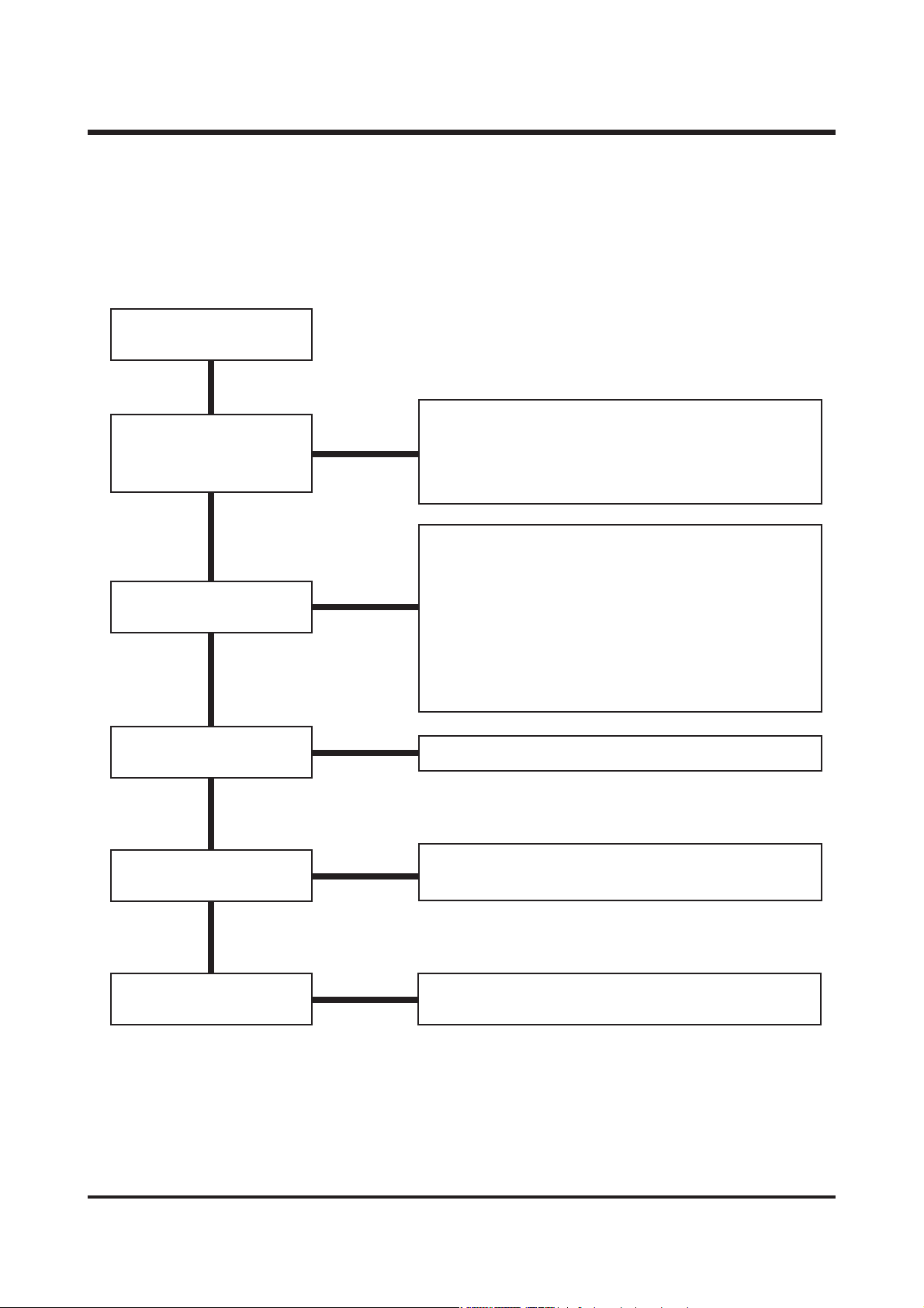
66.. PPrriinncciippaall ttrroouubblleesshhoooottiinngg
11)) DDooeess nn oott PPoowweerr oonn..
Check : Power input
(Battery, Adaptor, etc.)
Check the assembly
condition of various
Connectors!
Current electricity : 0mA
① heck soldering state : Between the Jack PCB and
the Power PCB (4point)
② Check soldering state : Battery contact (3point)
③ Check connection state between the Power PCB
and the Main PCB (J5)
① Check soldering state : Between the Jack PCB and
the Power PCB (4point)
-> Check parts : FB8, FB9, DP1 on Jack PCB.
② Check if the FUSE (FP-1, Q3601000701A) is Short
or Open!
-> Fuse Check (0Ω).
③ Check connection state between the Power PCB
and the Main PCB (J5)
④ Check soldering state : Battery contact (3point)
Power on, Circuit-short
(Overheating)
① Check parts : E6, C5, C6 on Jack PCB.
Current electricity :
280~330mA
Flash memory defect.
-> Upgrade the latest Firmware by I/F box
79 Page
86 Page
ⅥⅥ.. TT RR OOUUBBLL EESS HHOOOO TTIINN GG
76 Page
68 Page
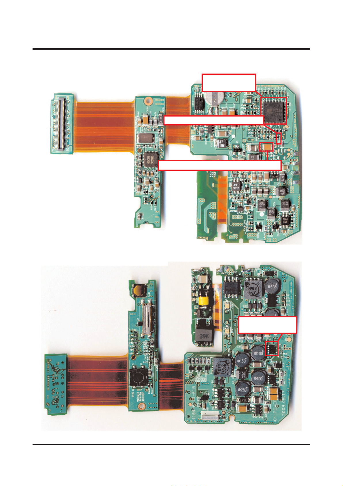
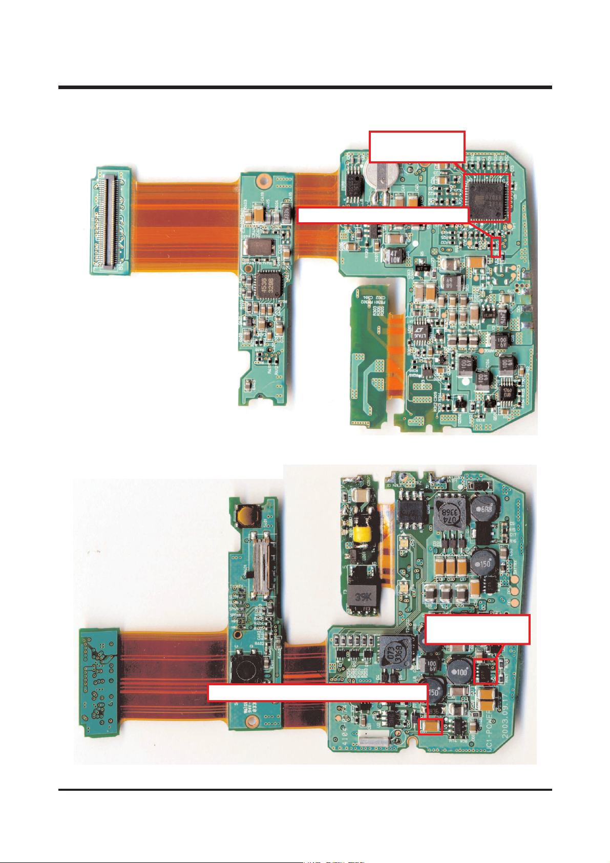
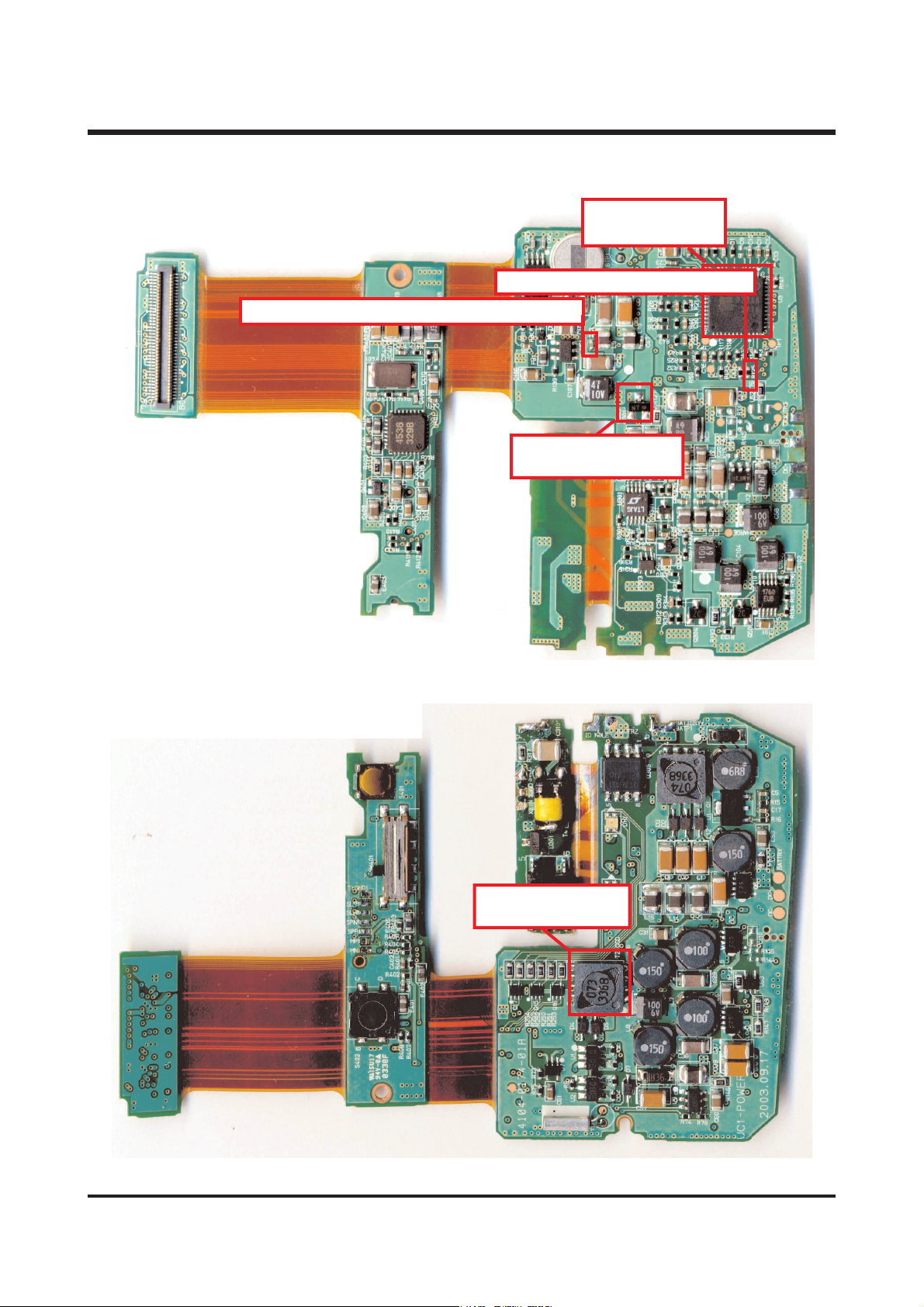
How to check the unit parts on the Power board
(Refer to 80~85 page)
Power PCB defect.
Page 2
79
8
1
1
12
13
24
25
36
3748
12
8024479
13
24
2536
37
48
1
1
1
4
8
5
4
8
5
6
45
14
85
ⅥⅥ.. TT RR OOUUBBLL EESS HHOOOO TTIINN GG
Check the connection state.
Check the connection state.
Check the connection state.
TFT LCD
g
PIN
J2
R2
D1
C14
C13
C17
R16
R15
C15
C16
R13
R12
E7
E6
C8
C10
C9
U1
C7
R1
R28
E5
C25
C24
C2
E8
LCD PCB
C1
PIN
C23
E9
R29
R31
R33
R35
R30
R32
R34
R36
L2
L1
J1
e
Jack PCB
C5
BAT
DP1
VCC
C6
C7
GNDP
FB8
E7
ID
J2
E6
FB9
FB2
R3
FB1
FB4
R2
FB3
E1
R4
E3
E2
FB6
FB7
E5
E4
FB5
c
FB2
C121
VJ DET
EAR201
GNDL1
NTSC1
GND1
USB DM
USB AT
USB DP
GND2
R158
R159
Q10
R154
Q6
R173
Q11
MICOM¡
HRESET
R156
R157
C102
R119R121
R118R120
C103
FB16
C104
R122
R134
D3
R131
R125
Q4
R132
R124
R135
Q5
D4
J4
C6
C5
FB7
C9
R28
U9
R29
R24
C118
FB18
R30
FB19
C123
C120
R151
C122
E2
C124
C119 C125
R91
R152
R153C126
C127
U10
TP7TP8
R99
C67
C60
R155
C70
FB21
CLKSEL
VCC3¡H
C64
C105
C145
C65
C146
C66
C63
U6
C97
C62
9 8 6 5 4 3 2 1
R104
FB13
C68
C58
R170
R140
J3
R133
R130
R126
FB9
C88
C86
D2
Q3
a
C19
PIN
C18
C6
E10
R3
C12
C4
C5
C3
L3
E11
C14
C15
C16
FB3
GND
R25
FB8
R19
R57
R61
R62
R23
R21
R26
R38
R59
C53
R96
J5
R27
R40
C55
R166
R95
I2C SC
I2C SD
E5
E4
R98
R100
R103
R102
R107
A
B
C
D
C61
L3
C59
Q9
C80
C78 C81
C87
FB11 FB14
Y3
C134C136
R172
R101 R171
R105
R113
R168
C57
L9
R106
C137
C138
C56
J
L
F
K
E
N
H
G
M
C99
C82
U5
C83
C93
R112
R111
C69
C73
L5L7L6
C79
C72
D1
C90
C74
R115
FB15
FB10
C71
C89
C91
J1
C101
FB12
C95
SPK. MIC. PCB
d
Main PCB
b
a Main(J1) - CCD F PCB
b Main(J3) - Barrel Main F PCB
c Main - Jack(J2 )
d Main(J5) - Power(J1 )
e Main(J4 ) -LCD(J1)
f Power - XE Tube, Main CON.
g LCD(J2) - TFT LCD
Main CON.
Power PCB
+
S401
f
SW401
T GND1
SLP1
SLN1
E406
SPN1
FB403
SPP1
R406
MP1
R404
MN1
R405
R401
C402C401
R402
E402
D
C
E401
S402
A
B
R407
R408
ID HOLE
C310
R317
XGND SVCC
T4
XETN
D301
SEC
FHVP
T3
SW
DCVIN
R254
R255
R252
R250
R251
R253
T2 CCD
Q17
Q15
Q16
D4
U7
R73
R6
R75
C61
BATTERY
D100
BATP1
BATTRZ
Q305
T1 LCD
C19
D14 D10
L15
C31
L6L8
C44
D5
U1
R8
D8
R13
U2
D7
C57
R12 R9
Y1
C5
R15
Q1
C17
R16
D2
D3
D1
C53
L12 L50
C1
C14
FB1
BATTERY
Q6
C54
DC
L13
L14
R74
DC
C110
Q2Q4
L5
R145
R144
C29
C40
R122
L7
R147 R148
C37
C38
C39
L16
R146
U9
C60
R78
PILOT
2003. 09. 27
UC1-POWER
Page 3
80
1-1) Power PWM IC Checking
※※ ww aarrnn iinn gg
11.. SSuupp ppll yy 33..33VV ffoorr aallll kk iinndd ss ooff ccoo nnttrroo ll ssiigg nnaallss..
22.. WWhheenn cchh eecckkii nngg ppaarrttss oonn PPoowweerr bb ooaarrdd aafftt eerr ddii ssaasssseemmbbllii nngg iitt ff rr oomm MM aaii nn BBoo aarrdd,,
bb ee ssuu rree ttoo ssuupp ppllyy 33..33VV 22AA ff oorr DD CC pp oowweerr..
1. Chcek Point
1) Power PWM IC Channel 1 : 8.5V / 5V / 3V
2) Power PWM IC Channel 2 : 18Vcc_Main
3) Power PWM IC Channel 3 : 3.3Vcc_Main
4) Power PWM IC Channel 4 : 15V / -7.5V_CCD
5) Power PWM IC Channel 5 : 5Vcc
※ If Output. any one output of Power Channels is not correct, all of the five channels will not work.
--
++
ⅥⅥ.. TT RR OOUUBBLL EESS HHOOOO TTIINN GG
ppoowweerr ssuuppppllyy :: 33..00VV 22..00AA
Page 4
81
①① rree mmoovvee RR11
②② II nnppuutt ccoonnttrrooll ssiiggnnaall oonn PPII NN NNOO..3311 ooff UU 33
③③ cchheecckk iiff 33VV ccoo mmee ss oouutt ooff CC 2211
▶▶ PPoowweerr PPWWMM IICC CChhaannnneell--11
TT11__LLCCDD
((QQ226600 11000011 440011AA))
QQ11 PPOOWWEERR BBJJTT
((QQ005500 22000011 330011AA))
ⅥⅥ.. TT RR OOUUBBLL EESS HHOOOO TTIINN GG
HHooww ttoo TTEESSTT
①① RReemmoovvee RR11
②② ii nnppuutt cc oonn ttrroo ll ssii ggnnaa ll oonn PPii nn
NNoo..3311 ooff UU 33
③③ CChheecckk iiff 33VV ccoommeess oouutt ffrroomm CC2211
→→ II ff nn oott,, rree ppllaaccee TT11__LLCC DD oorr QQ11
Page 5
82
②② cchheecckk iiff 11.. 88VV ccoo mmee ss oouutt ffrroomm CC22 77
▶▶ PPoowweerr PPWWMM IICC CChhaannnneell--22
UU33 PPWWMM IICC
((QQ112200 99000011 990011AA))
QQ22 FFEETT TTKKYY
((QQ005500 55000011 880011AA))
HHoo ww tt oo tt eesstt..
①① II nnppuutt ccoonntt rr ooll ssii ggnnaa ll oo nn RR 112255
②② cchheecckk iiff 11.. 88VV ccoo mmee ss oouutt ffrroomm CC22 77
→→ II ff nn oott,, rree ppllaaccee PPoo wweerr PPWWMM IICC oo rr QQ22
①① II nnppuutt cc oonntt rr ooll ssii ggnnaa ll RR1122 55
ⅥⅥ.. TT RR OOUUBBLL EESS HHOOOO TTIINN GG
Page 6
83
▶▶ PPoowweerr PPWWMM IICC CChhaannnneell--33
QQ44 FFEETT TTKKYY
((QQ005500 55000011 880011AA))
HHoo ww tt oo tt eesstt..
①① II nnppuutt ccoonntt rr ooll ssii ggnnaa ll oo nn RR 112255
②② cchheecckk iiff 33.. 33VV ccoo mmee ss oouutt ffrroomm CC33 77
→→ II ff nn oott,, rreepp llaaccee PPWWMM IICC oorr QQ44
①① II nnppuutt cc oonntt rr ooll ssii ggnnaa ll RR1122 55
②② cchheecckk iiff 33.. 33VV ccoo mmee ss oouutt ffrroomm CC33 77
UU33 PPWWMM IICC
((QQ112200 99000011 990011AA))
ⅥⅥ.. TT RR OOUUBBLL EESS HHOOOO TTIINN GG
Page 7
84
②② CChheecckk iiff 11.. 55VV ccoo mmeess oouutt ffrroomm CC443377
▶▶ PPoowweerr PPWWMM IICC CChhaannnneell--44
TT22__LLCCDD
((QQ226600 11000011 330011AA))
HHoo ww tt oo tt eesstt
①① II nnppuutt ccoonntt rr ooll ssii ggnnaa ll oo nn RR 112255
②② cchheecckk iiff 11.. 55VV ccoo mmee ss oouutt ffrroomm CC44 33
→→ II ff nn oott,, rree ppllaaccee PPoo wweerr PPWWMM IICC,,
TT22__LLCCDD oorr QQ55
QQ55 MMOOSS FFEETT
((QQ005500 55000011 990011AA))
UU33 PPWWMM IICC
((QQ112200 99000011 990011AA))
ⅥⅥ.. TT RR OOUUBBLL EESS HHOOOO TTIINN GG
①① II nnppuutt cc oonntt rr ooll ssii ggnnaa ll RR1122 55
Page 8

85
②② cchheecckk iiff 55VV ccoo mmeess oouutt ffrroomm CC55 22,, 5555,,
aa nndd CC5566..
▶▶ PPoowweerr PPWWMM IICC CChhaannnneell--55
QQ66 FFEETT TTKKYY
QQ00 55005500 0011880011AA
HHooww tt oo tteess tt HH ooww ttoo tteess tt
①① II nnppuutt ccoonntt rr ooll ssii ggnnaa ll oo nn RR 112255
②② cchheecckk iiff 55VV ccoommeess oouutt ffrroomm CC5522,, CC 5555,, CC5566
→→ II ff nn oott,, rreepp llaaccee PPWWMM IICC oorr QQ66
UU33 PPWWMM IICC
((QQ112200 99000011 990011AA))
ⅥⅥ.. TT RR OOUUBBLL EESS HHOOOO TTIINN GG
①① II nnppuutt cc oonntt rr ooll ssii ggnnaa ll RR1122 55
Page 9

86
2) Flashing defect.
<<QQ330055 IIGGBB TT CC hheecckk mmeett hhoodd >>
·1,2,3+4 = about 4.7KΩ
·1,2,3+5,6,7,8 and 4+5,6,7,8
= some KΩ ~ some MΩ
Check the XE TUBE.
Check the connection state between
the Trig F PCB and Power PCB.
Check the IGBT
79 Page
아래
부품
상태
aa
bb
cc
ee
ff
aa
bb
cc
dd
aaaa
aa
aa
aa
D301
Check the C307, C308
11
22
33
44
88
77
66
55
ⅥⅥ.. TT RR OOUUBBLL EESS HHOOOO TTIINN GG
TT44((QQ2277 004400 0011990011 AA))
TTRRII GG CCOO IILL
. a + c = about 87Ω
. b + c = about 1Ω
YY11((QQ2288 00220000 00880011 AA))
RRTTCC CCRRYYSSTTAALL
FFPP11 ((QQ 33660011 000000770011AA))
CChhii pp FF uussee((00ΩΩ))
DD11 00,,11 44((QQ0066 00110000 551100 11AA))
77 CCOOLL OORR LLEEDD
TT33((QQ2266 001100 0011550011 AA))
TTRRAANNSSFFOORRMMEERR
. c + d = about 0.3Ω
. e + f = about 52Ω
. a+b, a+c, a+e = Open
UU11((aa)):: 88..55 VV OOuu ttppuu tt(( ttoo LLCC DD))
UU22((aa)):: 55..oo VV OOuu ttppuu tt(( ttoo LLCCDD))
QQ22 PPII NN nnoo ..88((aa)) 11..88VV
((ttoo CCCC DD))
QQ44 PPII NN nnoo ..88((aa))
33..33VV ((ttoo MMaaiinn ))
QQ66 PPII NN nnoo ..88((aa)) 55..00VV
((ttoo IIGGBBTT,, AALL ,, FF LL EE DD))
QQ33 0055((QQ1144 00770000 00990011AA)) IIGGBBTT
FFll aasshhii nngg SSii ggnnaa ll ccoonntt rr ooll
Check the belows parts.
R310, R311, R312, R313,
R314, R315, R316, R317,
C309, C310, Q303, Q304,
Q305, T4
79 Page
①
②
③
④
③
Page 10

87
3) Charging defect.
Check the connection state between
the Trig F PCB and Power PCB.
Check the belows parts.
R307, R308, Q302, R309, T1,
R301, R302, R303, D301,U301
Check the Flash power circuit.
FB301, C301, C302 : 3.0VCC
FB302, C303, C304 : 3.3VCC
Check the charging voltage of
Main CON.(300~320V)
79 Page
CC3300 33
CC3300 11
FFBB 330011 FFBB3300 22
CC33 0022 CC33 0044
UU330011
RR3300 11
RR3300 22
RR3300 99
RR33 0077 RR33 0088
RR3300 33
ⅥⅥ.. TT RR OOUUBBLL EESS HHOOOO TTIINN GG
①
②
③
④
③
Page 11

88
ⅥⅥ.. TT RR OOUUBBLL EESS HHOOOO TTIINN GG
4) If Images cam be seen on LCD PANEL but Back Light is not turned on.
MMeeaa ssuu rree tthhee vvoo llttaaggee ooff BBLLPP && BBLLNN oonn bbootthh
ⓐ 9V ~ -11V : replace LCD Panel
ⓑ 0V :
check if D7 in the Power Board is 7.5V
check Main to Power connector (80 Pin).
DDiiggiittaall 88 BBiitt LLiinnee rreessiissttaannccee((RR2299--RR3366))
CClloocckk ccoonnnneeccttiioonn rreessiissttaannccee ((RR33))
OOppeenn // SShhoorrtt // ccoolldd ssoollddeerriinngg cchheecckk ((3333ΩΩ))
check J1 connection
and soldering(Open, Short)
AA ddddii ttiioonn dd eeff eeccttss oonn LLCC DD PPAARR ::
LCD becomes too bright while high current flows.
-> LCD F PCB connect defect (or F PCB CRACK)
LCD DRIVER IC SMT defect
Page 12

89
ⅥⅥ.. TT RR OOUUBBLL EESS HHOOOO TTIINN GG
5) In case LCD becomes all white.
check the connection and
soldering of J1 (Open, Short)
measure L1(3V), L2(5V) voltage.
If images cannot be seen after TV out,
In case LCD becomes all white and
Booting is not possible.
⇒ replace DSP Chip or Main Board
AA ddddiitt iioonnaall ddee ffeecctt ss oonn LLCC DD PPCCBB ::
When Keys don't work.
-> check the condition of LCD F PCB connection and
F PCB PATTERN CRACK,
Check if KEY PAD and KEY PATTERN of LCD PCB is
positioned on the right CENTER,
Check if there's any dirt on KEY PATTERN of LCD PCB.
Page 13

90
6) AUDIO Part
- Check if Audio is turned on from Menu.
- Be careful not to damage while soldering MIC & SPEAKER
ⅥⅥ.. TT RR OOUUBBLL EESS HHOOOO TTIINN GG
Check the condition of J1 connector’s
connection or soldering
(Short or Open)
--UU4400 11 AAUUDDIIOO CCOO DDEECC ((QQ338800 11000033 550011AA))
Check if PIN No.5 is High while using Audio.
When it is Low, check the connection with MICOM.
--UU11 22((QQ1122 0033000022 220011AA)) RR EEGGUULLAATT OORR
check PIN no.5 : 3.3V
Supply power to Audio circuit.
Page 14

91
7) ZOOM defect.
ⅥⅥ.. TT RR OOUUBBLL EESS HHOOOO TTIINN GG
II ff ll eennss iiss nn oott ww oorrkkii nngg pp rr ooppeerrllyy..
21 of J3 is 25Ω±5Ω, zoom motor is OK..
WWhheenn zzoooomm mmoo vveess ttoo tthhee eenndd
ooff TT// WW ppoo ssiitt iioo nn..
- Check the Q4, D3
- R131(300Ω), R132(18KΩ)
WWhh eenn FF OOCC UUSS--MM iiss nnoott
wwoorrkkii nngg pprroo ppeerrll yy ..
- Check the Q5, D4
WWhh eenn ppoowweerr oonn,, iiff iitt
mmoovveess ttoo tthh ee eenndd ww iitthh oouu tt
sstt oopppp iinn gg aatt tthhee wwoo ddee
ppoo ss iitt ii oonn ..
- Check the Q3, D2
Page 15

92
1. Remove the 1 screw at back cover side. 2. Remove the 4 screws at bottom side.
3. Remove the 4 screws at side. 4. Remove the back cover.
5. Remove the LCD EXIT F PCB from connector.
Remove the back cover ass’y.
77.. DDiissaasssseemmbbllee tthhee ccaammeerraa
ⅥⅥ.. TT RR OOUUBBLL EESS HH OOOO TTII NN GG
Page 16

93
6. Remove the front cover. 7. Besure to bleed the capacitor by the discharge
resistor.
8. Remove the electricity sheet. 9. Disconnect the CCD F PCB from the MAIN F
PCB.
10. Remove the 2 screws and take off the 11. Remove the OLPF.
CCD plate.
ⅥⅥ.. TT RR OOUUBBLL EESS HHOOOO TTIINN GG
Page 17

94
12. Don’t leave fingerprint on OLPF. 13. Remove the finder holder.
(fingerprint and substance matters)
14. Remove the 3 screws. 15. Remove the barrel ass’y.
16. Remove the one screw and connector 17. Remove the one screw and connector.
than resoldering 3 points.
ⅥⅥ.. TT RR OOUUBBLL EESS HHOOOO TTIINN GG
Page 18

95
ⅥⅥ.. TT RR OOUUBBLL EESS HHOOOO TTIINN GG
18. Remove the one screw and resoldering the 19. Resoldering the battery contacts.(3 points)
F PCB than remove the Main PCB.
20. Resoldering the power PCB and reflector. 21. Remove the power PCB.
22. Remove the 5 screws. 23. Remove the lead wires.
Page 19

96
24. Remove the TFT LCD. 25. Remove the 3 screws.
26. Remove the LCD PCB.
ⅥⅥ .. TT RR OOUU BBLL EESS HH OOOO TTII NN GG
Page 20

97
1. Remove the finder holder. 2. Remove the one screw.
3. Disconnect the F PCB by iron. 4. Remove the 3 screws.
5. Remove the lens base. 6. LENS BASE ASS’Y.
88.. DDiissaasssseemmbbllee tthhee bbaarrrreell
ⅥⅥ.. TT RR OOUUBBLL EESS HHOOOO TTIINN GG
Page 21

98
7. Remove the outer guide barrel. 8. Remove the outer cam barrel.
9. Remove the cam barrel. 10. Remove the zoomring.
11. Remove the 2nd lens ass’y. 12. 2nd LENS ASS’Y.
ⅥⅥ.. TT RR OOUUBBLL EESS HHOOOO TTIINN GG
Page 22

99
1. Assemble the 2nd lens barrel ass’y in the the zoomring.
Coincide the groove of 2nd lens barrel ass’y with the groove of zoomring.
2. Assemble the zoomring ass’y in the cam barrel.
Coincide the boss “a”and “b”of zoomring ass'y with “a”and “b”of cam barrel each other.
3. Assemble the cam barrel ass’y in the outer cam barrel.
Exact position after assembly is that the sutter F PCB is located on the boss of out cam barrel
together.
88.. AAsssseemmbbllee tthhee bbaarrrreell
aa
aa
ⅥⅥ.. TT RR OOUUBBLL EESS HHOOOO TTIINN GG
A
B
a
b
Page 23

100
6. Put the assembled OUT CAM BARREL ASS'Y in the OUT BARREL.
The boss of OUT CAM BARREL ASS'Y should be in line with the starting point of the screw thread
on the OUT GUIDE BARREL.
And Put the SHUTTER F PCB on the reflecting plate of PHOTO REFLECTOR.
7. Put the assembled OUT GUIDE BARREL ASS'Y and LENS BASE ASS'Y together.
The SHUTTER F PCB should be positioned in line with the slot for F PCB.
8. Finished.
ⅥⅥ.. TT RR OOUUBBLL EESS HHOOOO TTIINN GG
 Loading...