

Page 1

Samsung Electronics 13-1
13. Circuit Operating Description
13-1 Introduction to the product
13-1-1 Introduction
Miniket Photo is a digital camera equipped with a 5.25M CCD, and is capable of recording MPEG4 movies at
30fps in VGA. It is a multi-function gadget that can be used as a MP3 Player, a Mass Storage, a PC Camera
(webcam) and a Voice Recoder. This product has a memory slot for Mini-SD Card, and can be recharged
using a USB cable.
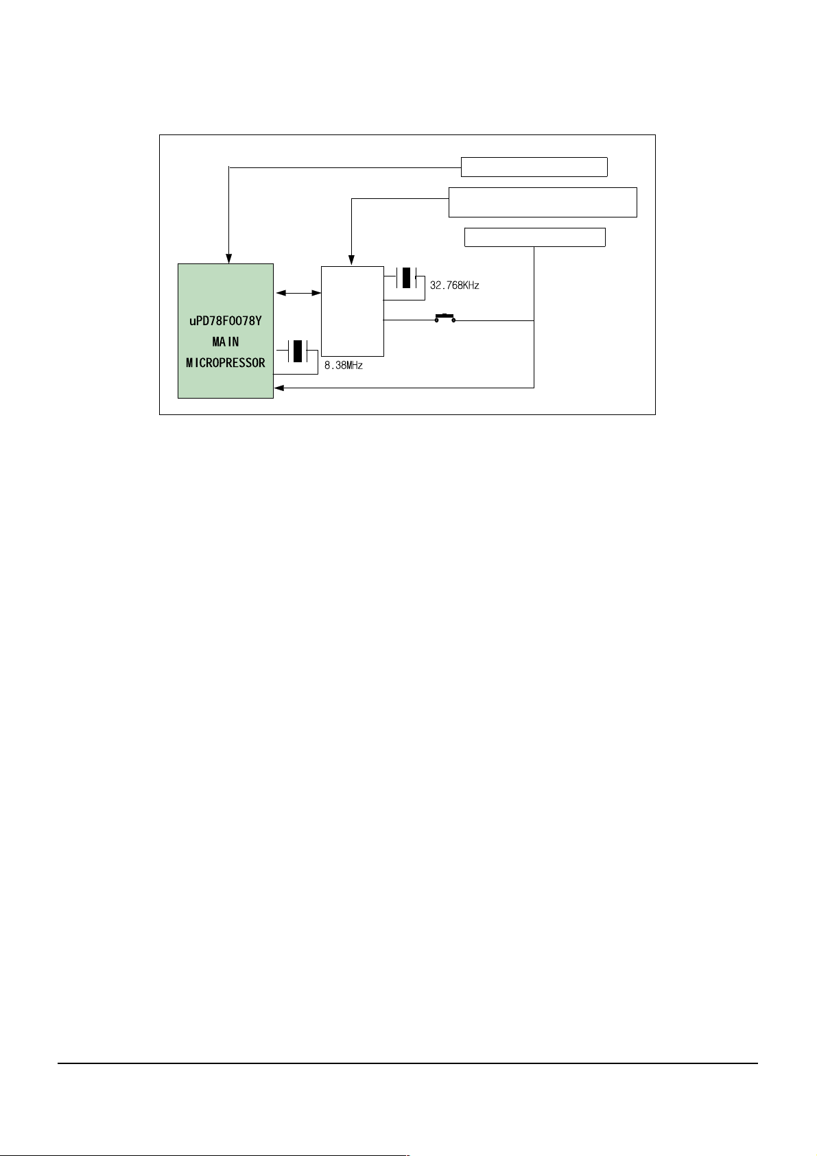
13-1-2 MICOM
1) MICOM CHIP FEATURE
ΠMICOM P/N : uPD78F0078Y
´ MAIN Clock : 8.38 MHz
ˇ MICOM Characteristics :
- 52 I/O port
- 8 channel 10 bit A/D port
- 4 channel serial port(2-channel UART, 2-channel 3wire)
- 1 channel IIC
- 6 channel Timer
- 26 vector interrupt
2) Control and Operating Description
Miniket Photo uses an 8-bit MICOM(uPD78F0078Y) to control "Key" inputs and for power
management. Its main clock runs at 8.38MHz; and rather than using 32.768KHz subsystem clock, a Real-Time
Clock(RTC) IC (RS5C372A) is connected to its I2C bus. Since Miniket Photo supports both Normal-Mode and
Stop-Mode, and a RTC IC is used to suspend all operations in the Stop Mode while power is supplied to the
MICOM. This will enhance the efficiency of limited battery capacity.
♦ SLEEP(HALT) MODE
In Wait State, Power Save Mode
- Stop Main Clock
- Stop Sub Clock -> System Clock and RTC Clock are used simultaneously
♦ STOP MODE
All operations are in suspend state. Voltage is being supplied and up to the last operation data
is stored in RAM
- Stop Main and Sub Clock
Page 2
Circuit Operating Description
13-2 Samsung Electronics
2) RESET Circuit diagram
Fig 13-1
TPS65520 2.9V Regulator
Back up Batter y 3.0V
Batter y/AC Adpter 3.6V
TPS65520 MICOM Reset
RTC
RS5C372
A
MENUAL RESET
RESET
Page 3
Circuit Operating Description
Samsung Electronics 13-3
3) MICOM and KEY CONTROL
Keys are controlled by MICOM. To use less MICOM ports, voltage dividing method is used and the voltage
values are inputted into MICOM's AD ports. AD Values are as shown below.
Table 13-1
MICOM
NO
PIN PORT
NO NAME MACRO
1
32 ANI 1 8WAY_AD2
5
31 ANI 2 8WAY_AD1
9
28 ANI 5 KEY_AD2
15
27 ANI 6 KEY_AD1
VOLTAGE Level
(2.9V base)
KEY NAME
TES18.1
EGAROTS51.12
MACCP16.03
REDROCERECIOV04
BMD18.1
3PM51.16
GEPM16.07
CSD08
UNEM0
YALPSID16.001
4YEKTOH51.111
3YEKTOH37.121
2YEKTOH43.231
1YEKTOH36.241
RETNE0
TFEL43.261
THGIR37.171
PU16.081
NWOD51.191
Page 4
Circuit Operating Description
13-4 Samsung Electronics
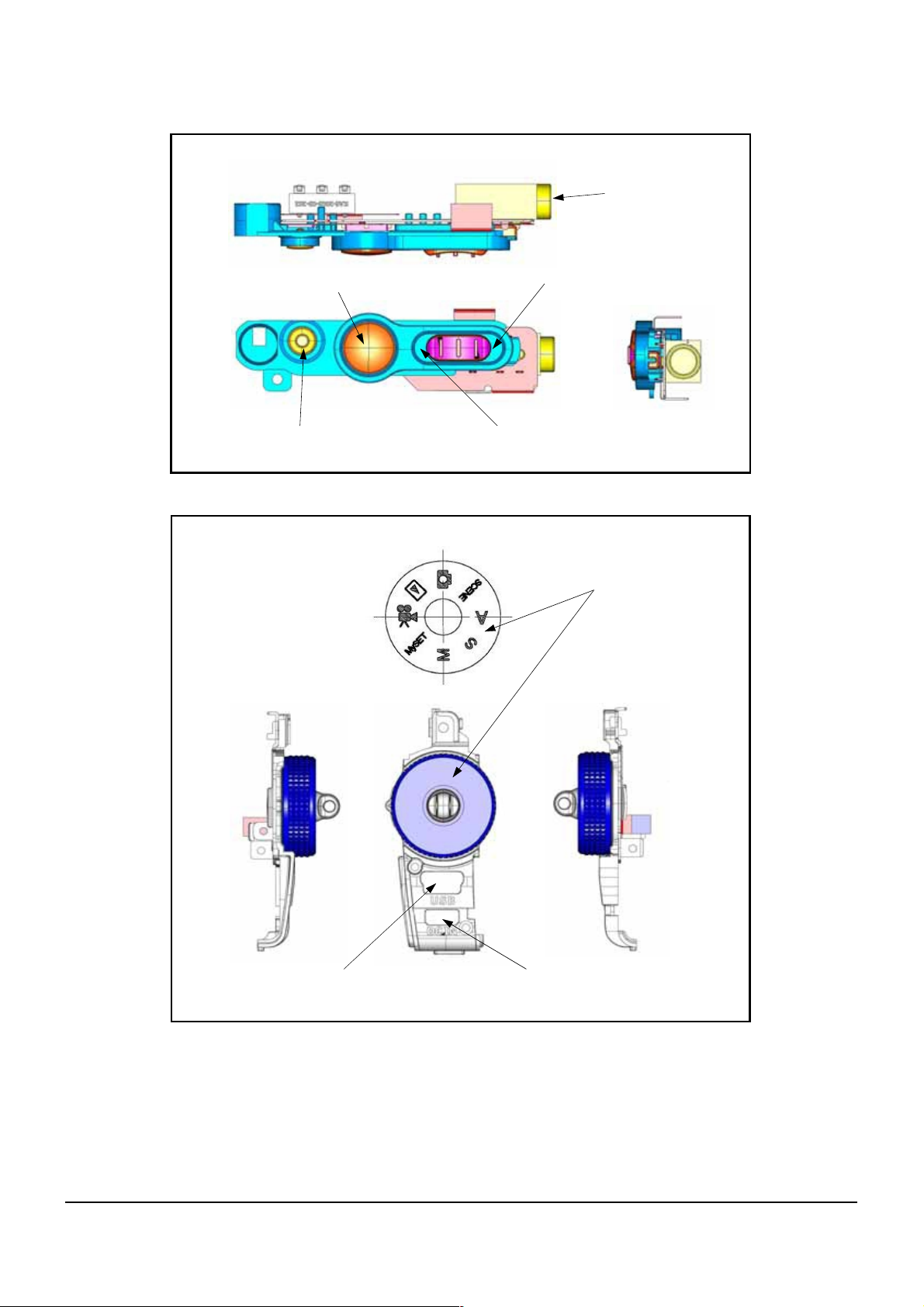
Fig 13-2
A/V JACK
B/T SHUTTER
B/T POWER_ON & PWR_LED
ZOOM_TELE
ZOOM_WIDE
ASSY POWER
8WAY MODE DIAL
USB JACK
DC JACK
ASSY MODE DIAL
Page 5

Circuit Operating Description
Samsung Electronics 13-5
4) MICOM and M3MML Interface
MICOM and M3MML are interconnected as shown below. They send and receive data regarding System Control.
In Miniket Photo, MICOM does not need Chip select signal to communicate with M3MML. M3MML establishes
communication with MICOM by sending out an interrupt signal; and whenever booting is done, M3MML
notifies to MICOM.
Fig 13-3
5) MICOM and CAMERA BARRIER CONTROL
MICOM checks PI signal from Lens Barrier, then send out a control signal to Motor Driver IC.
Motor Driver IC checks the signal and controls Motor's rotating direction. Interface between MICOM and Motor
Driver IC, Truth Table and Timing Chart are shown below.
Fig 13-4
Table 13-2
-
L
H
-
L
H
L
H
L
L
H
H
Z
H
L
L
Z
L
H
L
OFF
Forward Rotation
Reverse Rotation
Brake
Page 6

Circuit Operating Description
13-6 Samsung Electronics
6) MICOM and Back-Up
ΠIntroduction of Control
Power management for each mode must be done by controlling supplied power. Entering Stop Mode,
the minimum level of power is provided to protect backup data. MICOM controls power management
for each mode. It manages battery related signals, and switches to either Normal Mode or Stop Mode
by checking battery's voltage level that goes into an AD Port. In Miniket Photo, MICOM enters
Stop Mode when less than 3.3V of battery voltage is detected at the AD Port. MICOM can also
enter Stop Mode by Power Switch; however, it can wake-up only by the Power Switch (active Low).
´ H/W Interface Diagram
Fig 13-5
MICOM
M3MML
M3MML
DC-JACK
DC-JACK
(4.8V1A)
(4.8V1A)
Battery
Battery
(3.7V/820mAh)
(3.7V/820mAh)
Clock-Lithium
Clock-Lithium
(3V/3.4mAh)
(3V/3.4mAh)
RSTN(Mai n Res et)
RSTN(Mai n Res et)
P33/P41/P43
P33/P41/P43
Current Consumption : 10u A
Current Consumption : 10u A
TPS65520
TPS65520
BATT_CHARGER
BATT_CHARGER
RTC BLOCK
RTC BLOCK
BATT_SW_ DET
BATT_SW_ DET
MICOM
DSP_RESET
DSP_RESET
SI1/SO1/SCK1
SI1/SO1/SCK1
nMRESET
nMRESET
S/W Process
S/W Process
(CHARGE_CONTROL)
(CHARGE_CONTROL)
S/W Process
S/W Process
33Pin Voltage Level < 3.3V -->
33Pin Voltage Level < 3.3V -->
(1) Power off
(1) Power off
(2) BACK UP
(2) BACK UP
DC/DC CTL
DC/DC CTL
Power Enable
Vdd 0(VSTANDBY)
Vdd 0(VSTANDBY)
Vdd 1(VCC_MAIN3V)
Vdd 1(VCC_MAIN3V)
SDA0/SCL0
SDA0/SCL0
Memory-Map
Memory-Map
000H
000H
ROM
ROM
60KB
60KB
200H
200H
000H
000H
200H
200H
I:1024B
I:1024B
E:1024B
E:1024B
POWER CTL
POWER CTL
RAM
RAM
("L"->Off,
("L"->Off,
"H"->On )
"H"->On )
BLOCK
BLOCK
Page 7

Circuit Operating Description
Samsung Electronics 13-7
13-2 DC/DC (TPS65520)
13-2-1 Interface with MICOM
DC/DC IC is controlled by M3MML, and it communicates with M3MML via Serial Bus. Input voltage level and
On/Off control of DC/DC channels are done by MICOM. Default setting data gets stored in EEPROM.
Table 13-3
Table 13-4
13-2-2 TPS65520 Channel Summary
Characteristics of each channel of TPS65520 are shown below.
13-2-2 TPS65520 Operation Flow
Once power is supplied to the board, CH8 outputs 3.6V, which then becomes the reference voltage
for LDO-1 and LDO-2 to output 2.9V. Then this 2.9V becomes the reference voltage for MICOM.
At this point, when Power Key gets pressed, MICOM will receive POWER_ON signal. Upon the
reception of POWER_ON signal, MICOM will send out DD_ON signal to DC/DC IC (TPS65520),
then DC/DC IC will turn on all its channels from Ch1 to Ch7.
Pin No
C7
Pin Name
SYSDDON
K8,L8,K7,L7 Serial Bus
D7
LD04_ON
uPD78F0078-P56,SI3,SO3,SCK3
Connection
uPD78F0078-P55
uPD78F0078-P53
Control
Active High
Active High
NAME
CH-1
CH-2
CH-3
CH-4
CH-5
CH-6
CH-7
CH-8
LDO-1
LDO-2
LDO-3
LDO-4
LDO-5
Output Range
[V]
2.65 ~ 3.2 3V DSP, AUDIO, MC Vout1 = 1011 400 mA
1.1 ~ 1.8 1.8V DSP, DMB Vout2 = 0011 500 mA
4.5 ~ 5.2 5V CCD, Vout3 = 1101 500 mA
15.0 ~ 16.5 15V CCD Vout4 = 00 50 mA
-9.0 ~ -7.5 -7.5V CCD Vout5 = 00 50 mA
5.6 ~ 21.0 9.5V Backlight LCD Vout6B = 10 12 mA
2.5 ~ 3.2 2.5V DMB Vout7 = 1100 500 mA
8.5 ~ 13.5 8.5 ~ 13.5 LCD LDO5Vo = 10 36 mA
Output
Setting
Purpose Register Setting Current limit
Am081CCV~6.3CCV~6.3
Am639.29.2
Am06MOCIM9.29.2
Am42DCL1.31.3
Am021BMD1.31.3
Page 8

Circuit Operating Description
13-8 Samsung Electronics
13-3 AUDIO/VIDEO
13-3-1 AUDIO CODEC Operation
Audio Codec IC(AK4642) operates as a Master.
Fig 13-6
13-3-2 MIC Recording (Mono)
PMADL and PMADR bits set mono/stereo ADC operation.
Since MIC is mono, duplicate copy of Rch MIC input becomes Lch input during ADC data communication.
13-3-3 Audio Output
Stereo Line-out (LOUT/ROUT pins) are default Audio Output. When playing back a recorded
Voice or a MPEG4 file, Mono signals get duplicated; whereas MP3 files are played in Stereo.
DAC Master Mode
Page 9

Circuit Operating Description
Samsung Electronics 13-9
13-3-4 VIDEO Output
Video output and LCD output cannot be outputted at the same time. When A/V jack is inserted,
LCD display will automatically turns off, and M3MML's Pin Y14 outputs composite Video signals.
This output signals will be input to IC803's Pin #4 and 6dB amplification will occur. Then this
amplified signals will be inputted to IC801 (A/V Switch), IC801 will output the signals to A/V
Jack once the jack is detected.
TS3V330(A/V Switch) Control
TS3V330 is a Quad Video Switch, and is used for switching between A/V data output and
earphone output which allows us to use a single A/V Jack. The following function table
shows TS3V330 operations.
Table 13-5
Table 13-6
13-3-5 AV Jack / Earphone Classification
MICOM control for detecting Earphone Jack and A/V Jack is as shown below.
Input
#EN IN
Output D Function
Signal Name Connection I/O Control
JACK_ON
AV_JACK_DET
uPD78f0078 - P70
uPD78f0078 - AN13
O
I
Active Low
To recognize de-insertion of a Jack, this
signal needs to be always turned on
When JACK is inserted, AV_JACK_DET=L
When JACK is not inserted, AV_JACK_DET
=H
Check AD value for Jack insertion/deinsertion status.
1S=D1SLL
2S=D2SHL
tcennocsiDZXH
If AV Jack is inserted, JACK_EAR_DET = L
JACK_EAR_DET
OUT_SEL
AV_EAR_SEL
uPD78f0078 - P44
uPD78f0078 - P41
uPD78f0078 - P40
if Earphone Jack is inserted,
I
JACK_EAR_DET = H
During speaker output, if OUT_SEL = H
AV_JACK_DET = L, then set OUT_SEL =
O
L
If (AV_JACK_DET = L &&
JACK_EAR_DET = L) ,AV_EAR_SEL = L
(AV output)
O
If (AV_JACK_DET = L &&
JACK_EAR_DET = H),AV_EAR_SEL = H
(Earphone output)
Page 10

Circuit Operating Description
13-10 Samsung Electronics
13-4 CAMERA
13-4-1 CCD Circuit
1/2/5" 5.25M pixel CCD is used, and block diagram for CCD signal processing circuit is as shown below.
Fig 13-7
Timing Generator(TG) generates various pulses to allow CCD to operate. CCD receives pulses from
TG to output CCD image signals. After CCD outputs signals, sampling of these signals is
performed by CDS, then the sampled signals get converted to 10-bit digital signals by ADC. The
digitized signals then inputted to DSP for signal processing, then get stored into memory.
Miniket Photo uses a single chip solution that is comprised of Timing Generator (TG), CDS, PGA
and ADC. TG is controlled by DSP, and CDS/AGC/ADC are controlled by CPU itself.
+15V and -7.5V are supplied to CCD, then 11 vertical transmission register pulses (V1A, V1B, V2,
V3A, V3B, V4, V5A, V5B, V6, V7A, V7B), 2 horizontal transmission register pulses (H1, H2), RG
and electronic shutter signal (SUB) get inputted into CCD. To prevent "blooming" effect from
happening during a capture, CCDSHCNT signal is received from DSP. CCD operates according to
aforementioned signals, and it outputs CCD output signals.
CCD in Miniket Photo is ICX495CQZ in SMD type package. SMD package is chosen due to spatial
limitation. CCD's backside is shielded with a metal plate to reduce noise impact since CCD is very
noise sensitive.
Total pixel count : 2668(H) x 1970(V) apprx. 525M pixels
Effective Pixel count : 2616(H) x 1960(V) apprx. 513M pixels
Active Pixel count : 2608(H) x 1952(V) apprx. 509M pixels diagonal 7.19mm
Recommended Recording Pixel count :
2592(H) x 1944(V) apprx. 504M pixels diagonal 7.128mm
aspect ratio 4:3
Unit Cell Size : 2.2 µm(H) x 2.2µm(V)
AE/CAPTURE
CCD OUT
TG
Operation
CCD
CCD Drive Pulse
CDS/ADC
TG CONTROL
10BIT
CCD DAT
CDS/ADC
CONTROL
A
MICOM DS P
Page 11

Circuit Operating Description
Samsung Electronics 13-11
Fig 13-8
13-4-2 TIMING GENERATOR
CXD4802 is an IC which is comprised of TG (Timing Generator), VD (Vertical Driver), CDS (
Correlated Double Sampling), PGA (Programmable Gain Amplifier) and ADC (Analog to Digital
Converter).
CPU(M3MML) controls TG RESET through its designated RESET port.
TG receives 54MHz clock from a 54MHz Oscillator, and its internal PLL divides 54MHz clock
down to 27MHz then output the clock pulses to DSP and it also generates various pulses that CCD
requires as well. Default clock frequency for CCD is 27MHz. Once DSP receives 27MHz clock, it
counts the clock then outputs HD signals and VD signals back to TG accordingly. TG, then,
generates pulses in sync with HD and VD signals. CCD is equipped with RGB Bayer color filter.
+15 V, -7.5V
CCD
11 Vertical Transmission Pulses
2 Horizontal Transmission Pulses
Electronic Shutter, RG, CCDSHCNT
CCD Anal. OUt
Page 12

Circuit Operating Description
13-12 Samsung Electronics
MEMO
 Loading...