

Page 1
This Document can not be used without Samsung’s authorization.
Samsung Electronics
10-1
10. Schematic Diagrams
10-1 Battery/Charger/DC-DC (Main PCB)- - - - - - - - - - - - - - - - - - - - - - - - - - - -
10-2 MICOM (Main PCB)- - - - - - - - - - - - - - - - - - - - - - - - - - - - - - - - - - - - - - -
10-3 CPU/NOR/NAND/DDR/EEPROM/LCD/SD Slot (Main PCB) - - - - - - - - - - - - -
10-4 CCD TG/Motor (Main PCB) - - - - - - - - - - - - - - - - - - - - - - - - - - - - - - - - - -
10-5 Sloenoid/Strobe Connector (Main PCB) - - - - - - - - - - - - - - - - - - - - - - - - -
10-6 H264 Decoder/DMB Module I/F (Main PCB) - - - - - - - - - - - - - - - - - - - - - -
10-7 Audio DAC (Main PCB) - - - - - - - - - - - - - - - - - - - - - - - - - - - - - - - - - - - -
10-8 A/V Switching Logic/Video AMP (Main PCB) - - - - - - - - - - - - - - - - - - - - -
10-9 Function PCB (Function PCB) - - - - - - - - - - - - - - - - - - - - - - - - - - - - - - - -
10-2
10-3
10-4
10-5
10-6
10-7
10-8
10-9
10-10
For schematic Diagram
Note
Special note :
Most semiconductor devices are electrostatically sensitive and therefore require the special handling techniques described under the
“electrostatically sensitive (ES) devices” section of this service manual.
Note :
Do not use the part number shown on this drawing for ordering. The correct part number is shown in the parts list (may be slightly
different or amended since this drawing was prepared).
Important safety notices :
Components identified with the mark have the special characteristics for safety. When replacing any of these components.
Use only the same type.
Page 2
Schematic Diagrams
10-2
This Document can not be used without Samsung’s authorization. Samsung Electronics
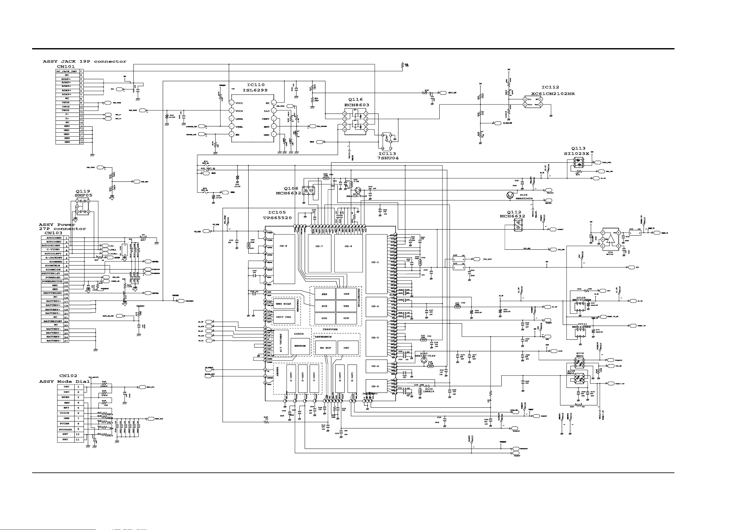
10-1 Battery/Charger/DC-DC (Main PCB)
Page 3
Schematic Diagrams
10-3
This Document can not be used without Samsung’s authorization.
Samsung Electronics
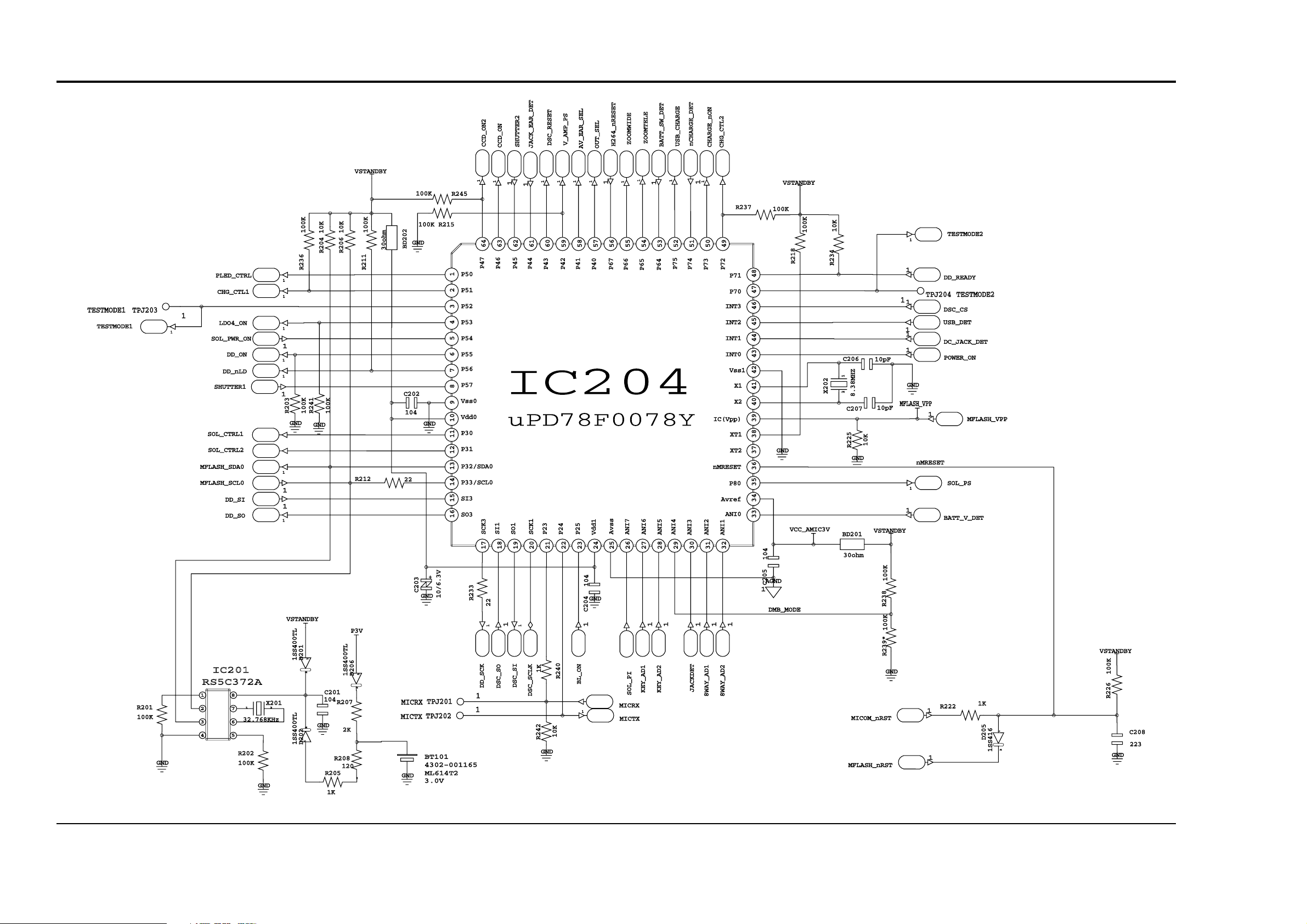
10-2 MICOM (Main PCB)
Page 4

Schematic Diagrams
10-4
This Document can not be used without Samsung’s authorization. Samsung Electronics
10-3 CPU/NOR/NAND/DDR/EEPROM/LCD/SD Slot (Main PCB)
AUDIO
VIEDO
Page 5

Schematic Diagrams
10-5
This Document can not be used without Samsung’s authorization.
Samsung Electronics
10-4 CCD TG/Motor (Main PCB)
VIEDO
Page 6

Schematic Diagrams
10-6
This Document can not be used without Samsung’s authorization. Samsung Electronics
10-5 Sloenoid/Strobe Connector (Main PCB)
Page 7

Schematic Diagrams
10-7
This Document can not be used without Samsung’s authorization.
Samsung Electronics
10-6 H264 Decoder/DMB Module I/F (Main PCB)
Page 8

Schematic Diagrams
10-8
This Document can not be used without Samsung’s authorization. Samsung Electronics
10-7 Audio DAC (Main PCB)
AUDIO
Page 9

Schematic Diagrams
10-9
This Document can not be used without Samsung’s authorization.
Samsung Electronics
10-8 A/V Switching Logic/Video AMP (Main PCB)
VIDEO
Page 10

Schematic Diagrams
10-10
This Document can not be used without Samsung’s authorization. Samsung Electronics
10-9 Function PCB (Function PCB)
1
2
J3
J3
CON2
CON2
VSTANDBY
R165
R165
20K-F
20K-F
R168
R168
30K-F
30K-F
R171
R171
50K-F
50K-F
R174
R174
100K-F
100K-F
R177
R177
300K-F
300K-F
C221
C221
104
104
SW3
SW3
SW PUSHBUTTON
SW PUSHBUTTON
SW4
SW4
SW PUSHBUTTON
SW PUSHBUTTON
SW5
SW5
SW PUSHBUTTON
SW PUSHBUTTON
SW6
SW6
SW PUSHBUTTON
SW PUSHBUTTON
SW7
SW7
SW PUSHBUTTON
SW PUSHBUTTON
SW8
SW8
SW PUSHBUTTON
SW PUSHBUTTON
R181
R181
100K-F
100K-F
KEY_AD2KEY_AD2
C224
C224
102
102
SW2
SW2
SW DIP-OCTAL
SW DIP-OCTAL
1
1
2
2
3
3
J2 CON50J2 CON50
VSTANDBY
C222
C222
104
R164
R164
100K-F
100K-F
R167
R167
27K-F
27K-F
R170
R170
39K-F
39K-F
R173
4
4
5
5
6
6
R173
82K-F
82K-F
R176
R176
270K-F
270K-F
104
KEY_AD1KEY_AD1KEY_AD1KEY_AD1KEY_AD1KEY_AD1KEY_AD1KEY_AD1
KEY_AD1
C225
C225
102
102
3
LED
LED
LED1
LED1
2 1
VSTANDBY
KEY_AD1
KEY_AD2
CHG_LED1CHG_LED1
CHG_LED2
1
2
3
4
5
6
7
8
9
10
11
12
13
14
15
16
17
18
19
20
21
22
23
24
25
26
27
28
29
30
31
32
33
34
35
36
37
38
39
40
41
42
43
44
45
 Loading...