

Page 1

2
CONTENTS
ⅠⅠ.. SSPPEECCIIFFIICCAATTIIOONN
1. CAMERA SPECIFICATION …………………………………………………………………………………………4
2. SYSTEM REQUIREMENTS ………………………………………………………………………………………5
3. TFT LCD PANEL MARK …………………………………………………………………………………………6
4. CONNECTION DIAGRAM …………………………………………………………………………………………8
5. IDENTIFICATION OF FEATURES …………………………………………………………………………………9
ⅡⅡ.. IINNSSTTAALLLLAATTIIOONN
………………………………………………………………………………………………11
ⅢⅢ.. EEXXPPLLOODDEEDD VVIIEEWW AANNDD PPAARRTTSS LLIISSTT
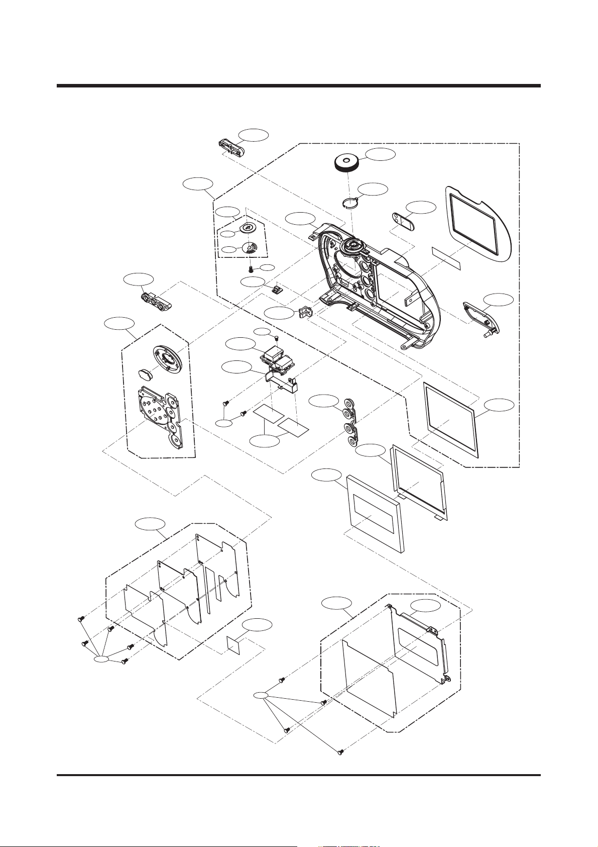
1. MAIN ASSEMBLY…………………………………………………………………………………………………16
2. BODY COVER ASSEMBLY ……………………………………………………………………………………18
3. BARREL ASSEMBLY ……………………………………………………………………………………………20
4. BARRIEL ASSEMBLY ……………………………………………………………………………………………22
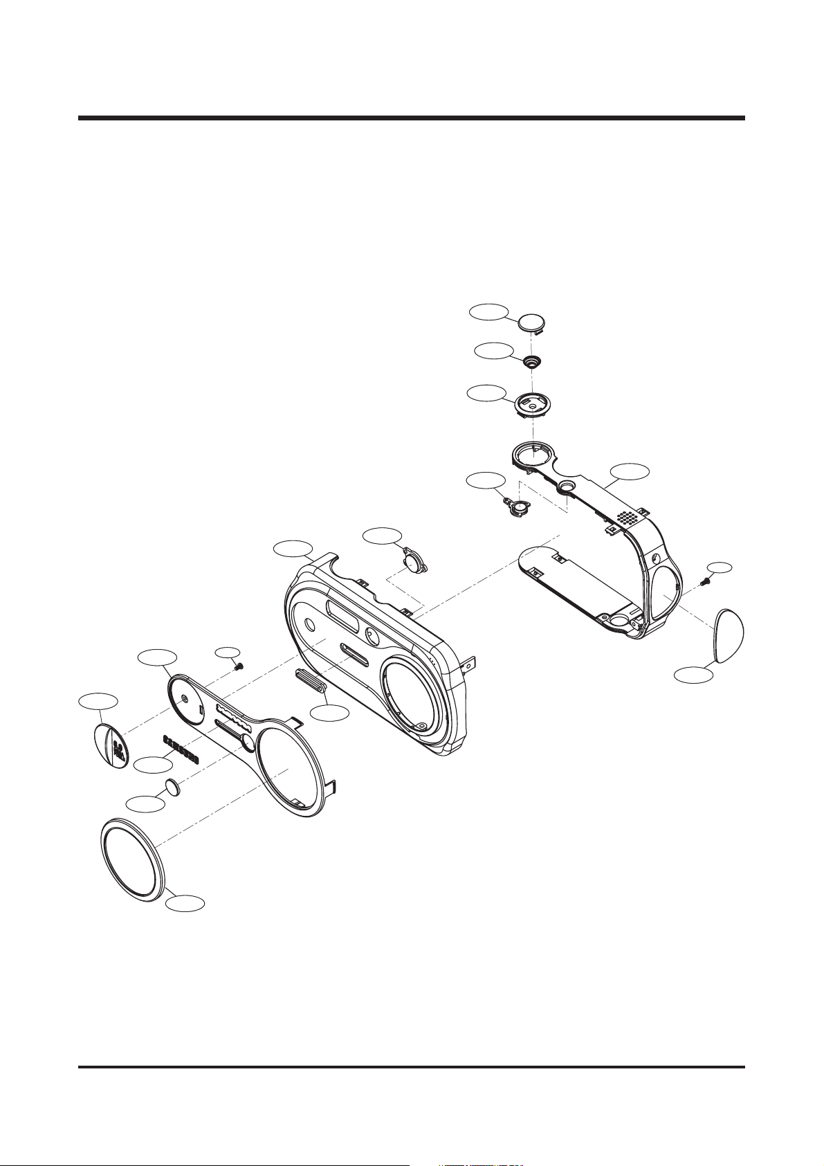
5. FINDER ASSEMBLY………………………………………………………………………………………………24
6. FRONT COVER ASSEMBLY ……………………………………………………………………………………26
7. BACK COVER ASSEMBLY ……………………………………………………………………………………28
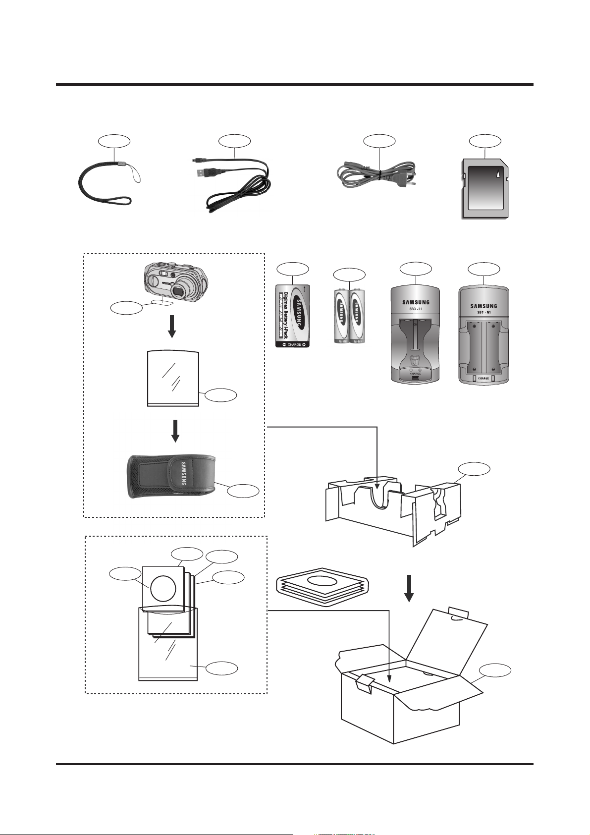
8. PACKING ITEM……………………………………………………………………………………………………30
ⅣⅣ.. AADDJJUUSSTTMMEENNTT
1. DIGITAL CAMERA SERVICE ……………………………………………………………………………………33
2. TUNNING ITEM BY CHANGED PARTS …………………………………………………………………………39
3. TUNNING …………………………………………………………………………………………………………40
4. ADJUSTMENT ……………………………………………………………………………………………………43
5. EEPROM Data Read/Write ……………………………………………………………………………………52
ⅤⅤ.. PPAATTTTEERRNN DDIIAAGGRRAAMM
1. PARTS ARRANGEMENT FOR EACH PCB ASS’Y
1) MAIN PCB ASSEMBLY_TOP …………………………………………………………………………… 62
2) MAIN PCB ASSEMBLY_BOTTOM …………………………………………………………………………63
3) POWER PCB ASSEMBLY_TOP ……………………………………………………………………………64
4) POWER PCB ASSEMBLY_BOTTOM ………………………………………………………………………65
5) SENSOR PCB ASSEMBLY_TOP ……………………………………………………………………………66
6) SENSOR PCB ASSEMBLY_BOTTOM ………………………………………………………………………67
7) STROBE PCB ASSEMBLY_TOP ……………………………………………………………………………68
8) STROBE PCB ASSEMBLY_BOTTOM ………………………………………………………………………69
9) USBDC PCB ASSEMBLY_TOP ……………………………………………………………………………70
10) USBDC PCB ASSEMBLY_BOTTOM ………………………………………………………………………71
11) TRANSFER PCB ASSEMBLY…………………………………………………………………………………72
12) UI PCB ASSEMBLY …………………………………………………………………………………………73
Page 2

3
ⅥⅥ.. CCUURRCCUUIITT DDIIAAGGRRAAMM
1. BLOCK DIAGRAM…………………………………………………………………………………………………74
2. CIRCUIT DIAGRAM
1-1) ZORAN COACH-6M ………………………………………………………………………………………75
1-2) ZORAN COACH-6M ………………………………………………………………………………………76
2) LCD DRIVER TPG018A ………………………………………………………………………………………77
3) MOTOR DRIVER M50234HP ………………………………………………………………………………78
4) SDRAM/NAND…………………………………………………………………………………………………79
5) SONY TG/AFE/VD CXD4801GA ……………………………………………………………………………80
6) MAIN POWER BD9733KN ……………………………………………………………………………………81
7) POWER_L6920 ………………………………………………………………………………………………82
8) SENSOR ………………………………………………………………………………………………………83
9) STROBE ………………………………………………………………………………………………………84
10) TRANSFER …………………………………………………………………………………………………85
11) UI………………………………………………………………………………………………………………86
12) USBDC ………………………………………………………………………………………………………87
ⅦⅦ.. TTRROOUUBBLLEESSHHOOOOTTIINNGG
1. CHECK LIST FOR REPAIRING …………………………………………………………………………………88
2. MAIN TROUBLESHOOTING
1) POWER ON DEFECT …………………………………………………………………………………………89
2) FLASH DEFECT ………………………………………………………………………………………………93
3) CHARGE DEFECT ……………………………………………………………………………………………95
4) Defect related with CCD ……………………………………………………………………………………97
5) Defect related to LCD ………………………………………………………………………………………99
6) Defect related to ZOOM……………………………………………………………………………………100
7) Defect related to the AUDIO ……………………………………………………………………………101
8) Defect related to card ……………………………………………………………………………………102
3. HOW TO DISASSEMBLY ………………………………………………………………………………………103
Page 3
4
ⅠⅠ..SSPPEECCIIFFIICCAATTIIOONN
11.. CCAAMMEERRAA SSPPEECCIIFFIICCAATTIIOONN
Type 1/1.8" CCD
Effective Pixel Approx. 7.0 Mega-pixel
Total Pixel Approx. 7.2 Mega-pixel
SHD Lens f = 7.7 ~ 23.1mm
(35mm film equivalent : 38~114mm)
F No. F2.7 ~ F4.9
Still Image mode : 1.0X ~ 5.0X
Play mode : 1.0X ~ 10.0X (depends on image size)
Optical Viewfinder Real image optical viewfinder
LCD Monitor 2.0" color TFT LCD
Type TTL auto focus
Normal : 80cm ~ infinity
Macro : 4~80 cm(Wide), 25~80cm(Tele)
Type Mechanical and Electronic shutter
Speed 15 ~ 1/2,000 sec
Program AE, Aperture priority AE, Shutter Speed priority AE, Manual AE,
Metering: Multi, Spot
Compensation ±2.0EV (0.5EV steps)
ISO Equivalent Auto, 100, 200, 400
Shutter Speed : 15 ~ 1/2000 sec. selectable
F No. : F2.7 ~ F4.9 selectable
Modes Auto, Auto & Red-eye reduction, Fill-in flash, Slow sync, Flash off
Range 0.25~3.0m(Wide), 0.25~2.0m(Tele)
Recharging Time About 6.0sec
Sharpness Soft, Normal, Vivid
Effect Normal, B&W, Sepia, RGB
White Balance Auto,Daylight,Cloudy,Sunset,Fluorescent_H,Fluorescent_LTungsten,Custom
Voice Recording (Max. 1hour)
Voice Memo in Still Image (max. 10 sec.)
Date Imprinting Date&Time, Date, Off (user selectable)
Modes : Program, Auto, Scene, AS priority, Manual, Voice Recording,
Night
Continuous : Single, Continuous, AEB
Self-timer : 2 sec., 10 sec., Double self timer (10sec. & 2sec)
With audio (recording time : memory capacity dependent)
Size : 640x480, 320x240, 160x120
Frame rate : 30 fps, 15 fps
Pause Function in Movie Clip
Internal : 32MB flash memory
External Memory Slot : SD Card/MMC
(Up to 512MB guaranteed)
Image Sensor
Lens
Digital Zoom
Focal Rength
Range
Still Image
Movie Clip
Media
Manual
Focusing
Shutter
Exposure
Flash
Control
Shooting
Voice Recording
Storage
View finder
Page 4
5
Ⅰ. SPECIFICATION
PC with processor better than MMX Pentium 233MHz (XP : Pentium II 300MHz)
Windows 98/98SE/2000/ME/XP
For Windows Minimum 32MB RAM (XP : 128MB)
140MB of available hard-disk space, USB port, CD-ROM drive,
800×600 pixels, 16-bit colour display compatible monitor
(24-bit color display recommended)
Power Mac G3 or later
Mac OS 9.0 ~ 10.2
For Macintosh Minimum 64MB RAM
110MB of available hard-disk space, USB port, CD-ROM drive,
QuickTime 4.0 or later for Movie Clip
22.. SSYYSSTTEEMM RREEQQUUIIRREEMMEENNTTSS
Still Image : JPEG (DCF), EXIF 2.2, DPOF 1.1, PictBridge 1.0
Movie Clip : AVI (MJPEG) Audio : WAV
3072 : 3072x2304, 2816 : 2816x2112
2592 : 2592x1944, 2272 : 2272x1704
2048 : 2048x1536, 1600 : 1600x1200
1024 : 1024x768, 640 : 640x480
3072 : Superfine 7, Fine 14, Normal 21
2816 : Superfine 8, Fine 16, Normal 25
2592 : Superfine 10, Fine 19, Normal 30
2272 : Superfine 13, Fine 26, Normal 39
2048 : Superfine 16, Fine 32, Normal 47
1600 : Superfine 26, Fine 52, Normal 65
1024 : Superfine 64, Fine 95, Normal 127
640 : Superfine 162, Fine 205, Normal 244
* These figures are measured under Samsung’s standard conditions and
may vary depending on shooting conditions and camera settings.
Type Single image, Thumbnails, Slide show, Movie Clip
Editing Trimming, Rotating, Resizing
Digital output connector : USB 1.1
Audio : Mono
DC power input connector : 3.3V
Primary Batteries: 2 x AA alkaline, or CR-V3(Lithium) battery
Secondary Batteries: 2 x Ni-MH(Samsung SNB-2312 recommended),
Samsung SBP-1303(Lithium Ion)
AC Adapter(optional): SAC-32 (DC 3.3V, 2A)
* Included battery may vary depending on sales region.
Dimensions (WxHxD) 109.8 x 56.8x 34.1 mm
Weight 166g (without batteries and card)
Operating Temperature 0 ~40 °C
Operating Humidity 5 ~ 85%
Camera Driver Storage Driver (Windows98/98SE)
Application Arcsoft PhotoImpression, Digimax Viewer, Digimax Reader
Power Movie Clip(Pause Function in Movie Clip & VGA 30fps),
One touch Manual Function(A/S/M Button), 4cm Macro,
Bright Pilot Lamp(Communication with user), Various Scene Modes,
RGB Color Effect, Voice Recording, Samsung High Definition(SHD) Lens,
Pictbridge Printing, 32MB Internal Memory
Capacity
(32MB0
File Format
File Format
Storage
Power Source
Image Play
Interface
Software
Special Features
Page 5
6
Ⅰ. SPECIFICATION
No. Description Icons
1 Battery
3 Continuous shot AEB
4 Flash
5 Self-timer
6 Macro
7 Metering
8 Memory card inserted indicator
9 Auto focus frame
10 Camera shake warning
11 Date/Time 2005.01.01 01:00 PM
12 Exposure compensation
13 White Balane
14 ISO
15 Sharpness
16 Image quality
17 Image size 3072, 2816, 2592, 2272, 2048, 1600, 1024, 640
Number of abailable shots remaining 12
Remaining time(Movie clip/Voice recording) 00:00:44/00:59:00
19 Voice memo
20 Optical zoom/Digital zoom rate
33.. TTFFTT LLCCDD PPAANNEELL MMAARRKK
■ Recording mode
②
③
④
⑤
⑥
⑦
⑧
⑫
⑬
⑭
⒃
⑮
⒔
⒕
⑨
⑩
⑪
⒗
⒖
①
Recording mode
2
18
Page 6
7
Ⅰ. SPECIFICATION
■ play mode
No. Description Icons
1 Battery
2 Play mode
3 File Type
4 Voice memo
5 Protect indicator
6 DPOF indicator
8 Storde image number
①
⑥
⑦
②
③
④
⑤
SIZE : 3072X2304 Size
AV : F 2.7 Aperture value
TV : 1/30 Shutter speed
ISO : 100 ISO sensitivity
FLASH : OFF Whether or not the
flash is used.
DATE : 2005/01/01 Recording date
9
SSIIZZEE :: 22881166XX22111122
AAVV :: FF22..77
TTVV :: 11//3300
IISSOO :: 110000
FFLLAASSHH :: OOFFFF
DDAATTEE :: 22000044//0088//0011
Page 7
8
Ⅰ. SPECIFICATION
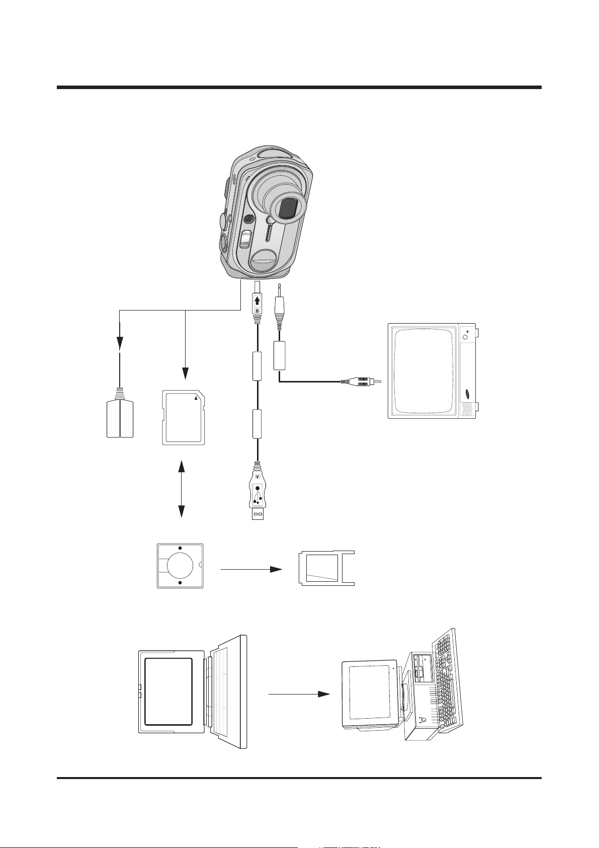
44.. CCOONNNNEECCTTIIOONN DDIIAAGGRRAAMM
Video Cable
AC Adaptor
SD Card
Card Reader
TV Monitor
USB Cable
PC Card Adaptor
Lap top
IBM / MAC
Page 8
9
Ⅰ. SPECIFICATION
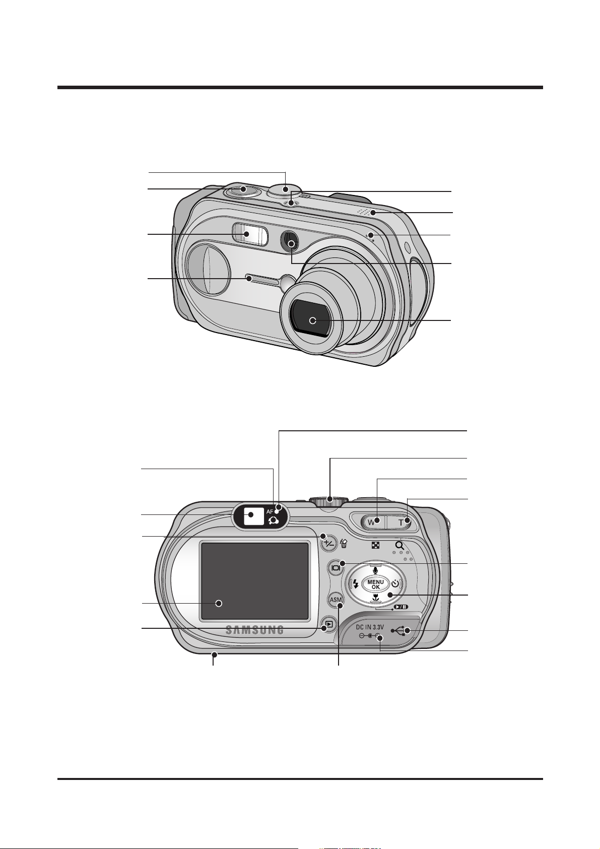
55..
IIDDEENNTTIIFFIICCAATTIIOONN OOFF FFEEAATTUURREESS
View finder
Autofocus indicato
lamp(Green)
Flash indicator
lamp(Red)
Zoom W button
(Thumbnail)
Mode dial)
Zoom T button
(Digital zoom)
LCD button
5 function button
USB connection
port
DC input connection
port
LCD monitor
+,-/DELETE
button
Plasy mode button
Tripod socket
ASM(Manual &Scene mode)button
Shutter button
Power button
Microphone
Function lamp
Speaker
Lens
Mode dial
Viewfinder
Flash
Page 9
10
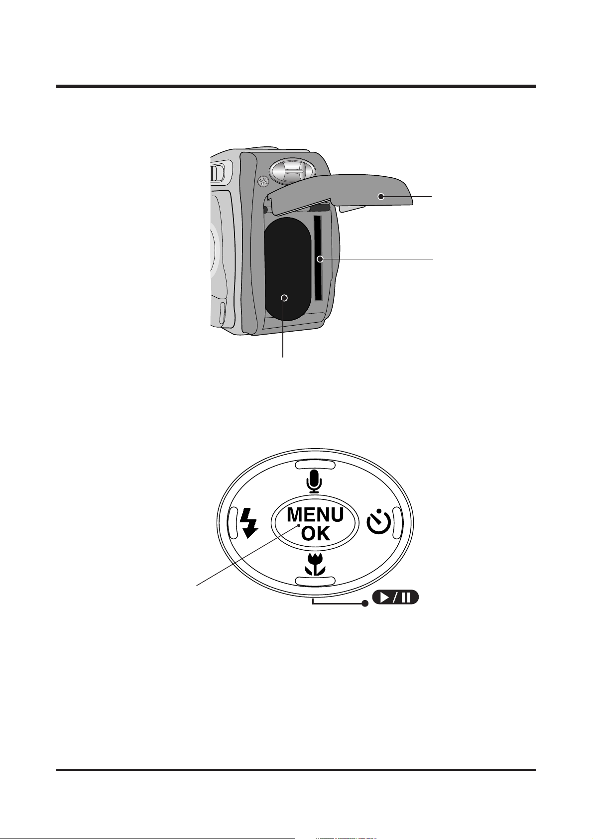
Ⅰ. SPECIFICATION
FLASH/
LEFT button
MENU/OK button
MACRO/DOWN button
SELF-TIMER/
RIGHT button
Voice memo/UP button
Battery chamber
Battery chamber cover
Memory card slot
Page 10
ⅡⅡ.. IINNSSTTAALLLLAATTIIOONN
11
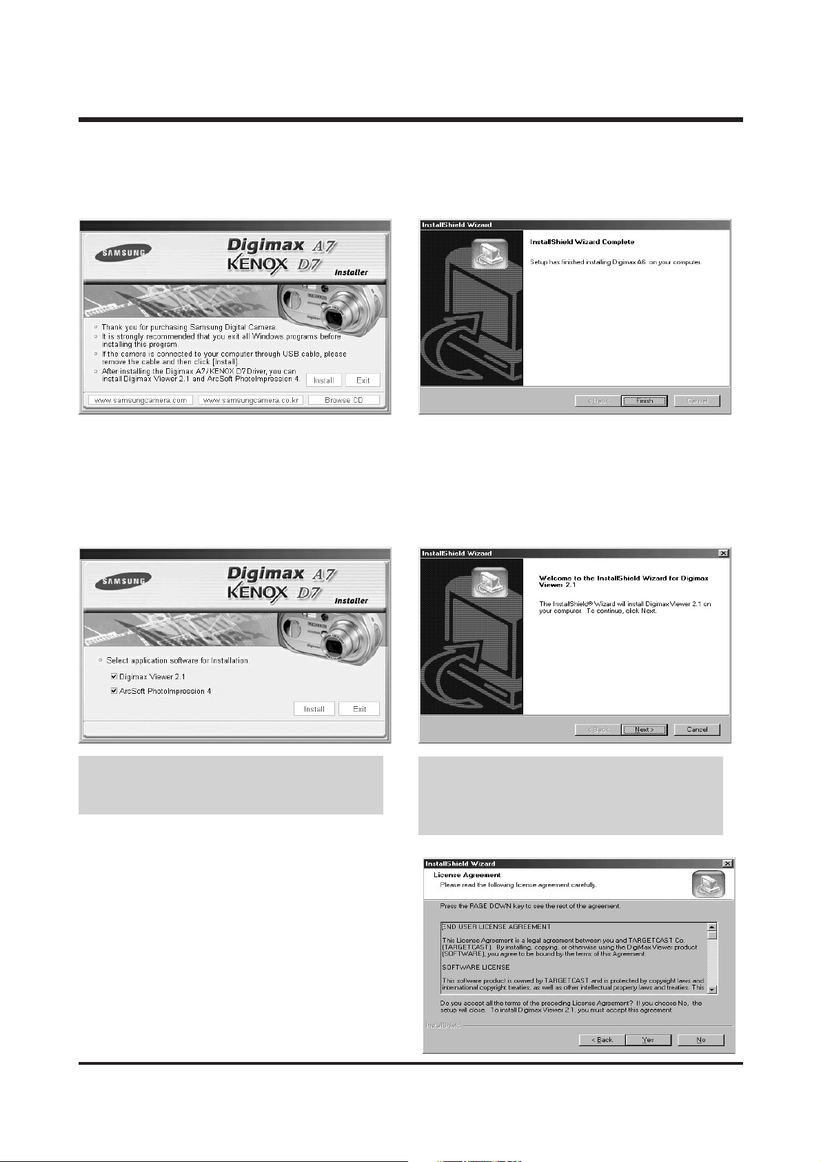
1. Click the [Install] menu in the Autorun frame.
The camera driver is installed automatically.
2. Camera driver installation is complete.
Click the [Finish] button.
3. A window for which you can select application
software will be displayed. Select the application
program and click the [Install] button.
Refer to page 96 for more information about the
application program.
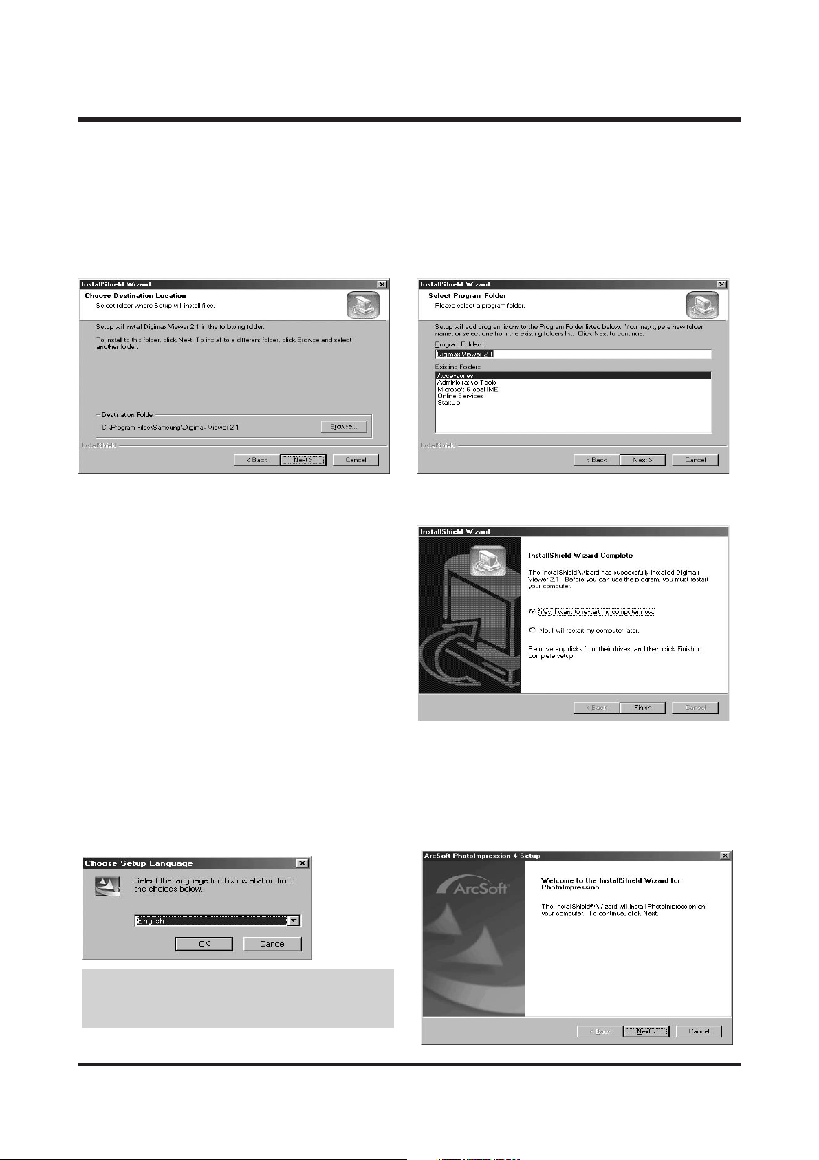
4. Install Digimax Viewer.
Click [Next >] button.
5. The Software License Agreement window will
be displayed. If you agree to this, click [Yes],
the window will then move to the next step.
If you disagree, click [No] and the installation
program will be canceled.
● If you select [Exit] at the step 3, the appli-
cation program installation will be cancelled.
● If you select [Cancel] at step 4, a window
for installing PhotoImpression will be displayed.
Page 11
12
Ⅱ. INSTALLATION
6. A destination selection window will open.
Click [Next >]. To copy to the files to another
folder, click [Browse..] and choose a folder you
want.
7. A window will open, asking you to choose a
folder to which program icons will be added.
Click [Next >] button. If you want to add the
program icons to a different folder, choose
another folder, and then click [Next >] button.
8. Digimax Viewer installation is successfully completed. Click the [Finish] button to install
PhotoImpression. The system will not reboot
even the [Yes, I want to restart the computer
now] option is selected.
* The frame 8 may not appear according to
the system requirements.
9. The PhotoImpression installation window will be
displayed as shown alongside. Click the [OK]
button.
● If you select [Cancel] at step 9, a window for
installing Digimax Reader will be displayed.
10. A Welcome window will be displayed.
Click the [Next >] button.
Page 12
13
Ⅱ. INSTALLATION
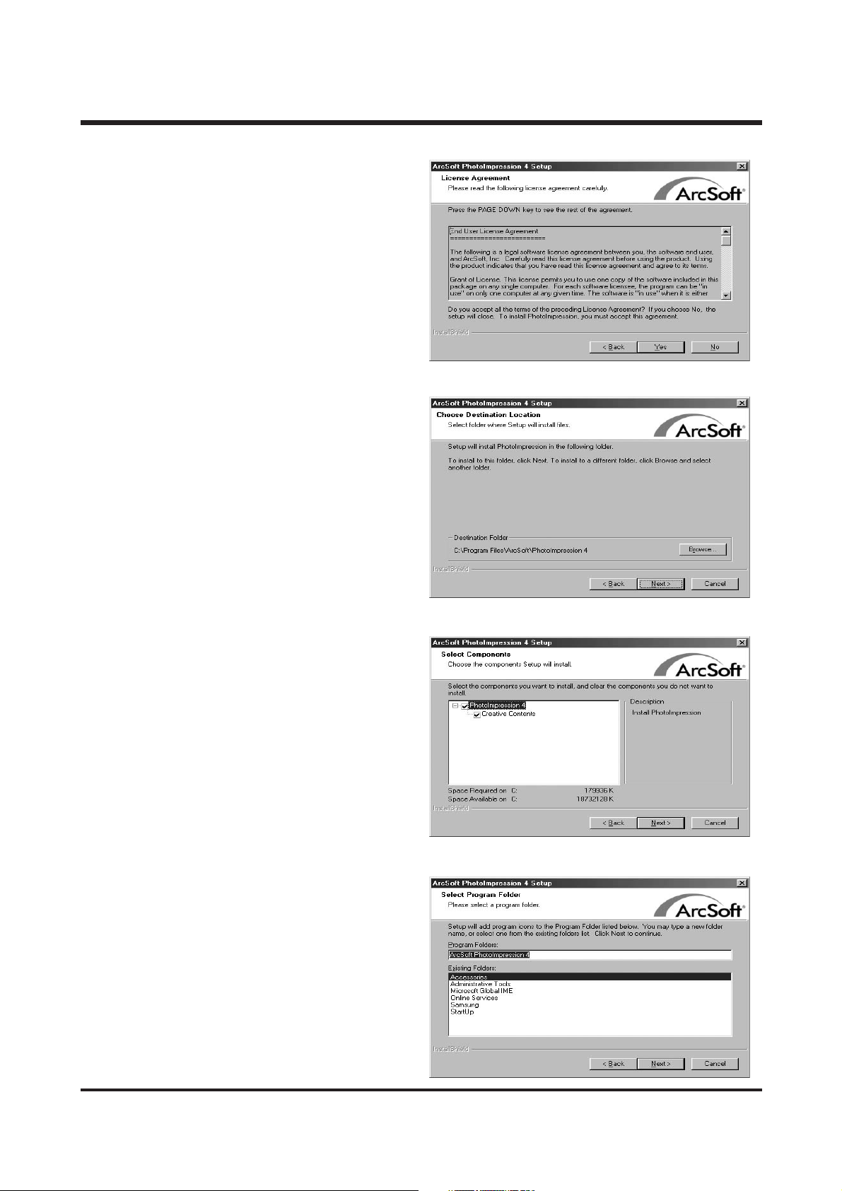
11. The Software License Agreement window will
be displayed. If you agree to this, click [Yes],
the window will then move to the next step.
If you disagree, click [No] and the installation
program will be canceled.
12. A destination selection window will open. Click
[Next >]. To copy to the files to another
folder, click [Browse...] and choose a folder
you want.
13. The [Select Components] window will appear.
Click [Next >] button.
14. A window will open, asking you to choose a
folder to which program icons will be added.
Click [Next >] button. If you want to add the
program icons to a different folder, choose
another folder, and then click [Next >] button.
Page 13
14
Ⅱ. INSTALLATION
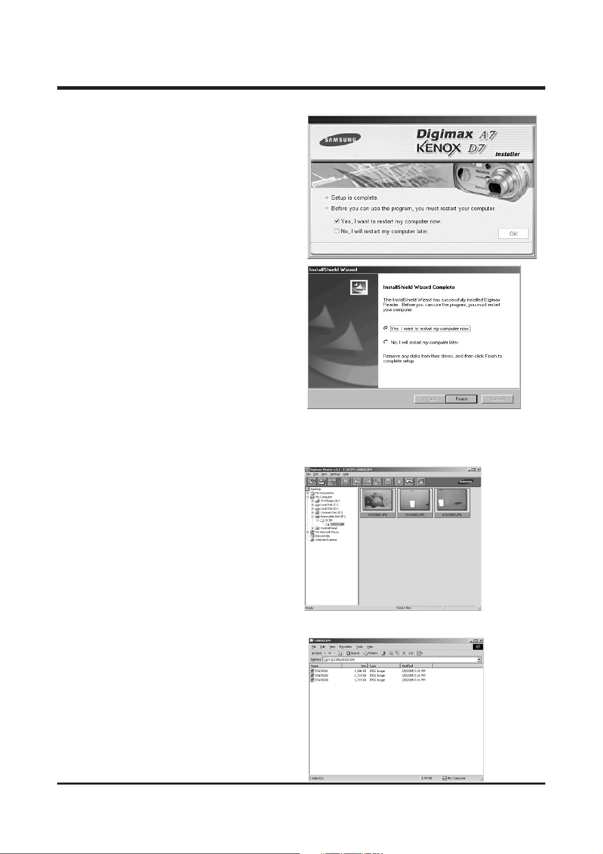
15. Installation is complete. To apply changes,
you must restart the computer.
Select [Yes, I want to restart my computer
now], and then click [OK].
* The frame 15 may be displayed according to
the system requirements.
Click the [Finish] button to restart the computer.
16. After restarting the computer, connect the PC to the camera with the USB cable.
17. Turn the camera power on. [Found New
Hardware Wizard] will open and the computer will recognise the camera.
* If you have ever installed an image viewer
program or your OS is Windows XP, an
image viewer program will open. If the
image viewer program opens, the camera
driver was setup successfully.
18. If you can see [Removable Disk] under
[My computer], the camera driver installation
was successful. Now you can transfer image
files from the camera to PC via the USB
cable.
Page 14

15
Ⅱ. INSTALLATION
● If you have installed the camera driver, [Found New Hardware Wizard] may not open.
● On a Windows 98 or 98 SE system, the Found New Hardware Wizard dialog box opens and a window
asking you to select a driver file may appear. In this case, specify
"USB Driver" in the CD supplied.
● When connecting the camera to your PC, it is recommended that you use an AC power adapter.
● Before connecting the camera to the PC, You should first install the camera driver.
● After installing the camera driver, you have to restart your PC.
● If you connect the camera to the PC before installing the camera driver, the [Found New Hardware
Wizard] will open.
In this case, cancel the [Found New Hardware Wizard] and disconnect the camera.
Install the camera driverand connect the camera to the PC again.
● Should the computer not find the camera driver after installation, please try one or more of the following measures.
1. Delete the camera driver, and re-install the driver.
2. Refer to FAQ to check for a possible solution to the problem.
3. If your PC’s central processing unit is VIA chip (This is shown in the USB Host Controller), download
the patch file from the Samsung Camera web page. (http://www.samsungcamera.com)
Page 15
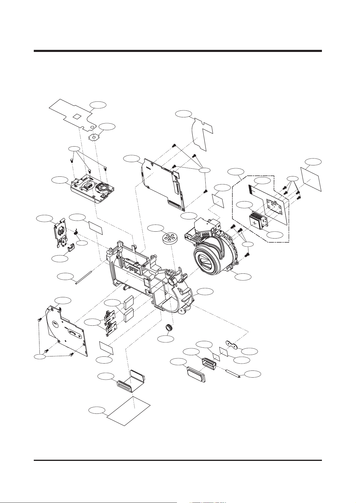
ⅢⅢ.. EEXXPPLLOODDEEDD VVIIEEWWSS AANNDD PPAARRTTSS LLIISSTT
1616
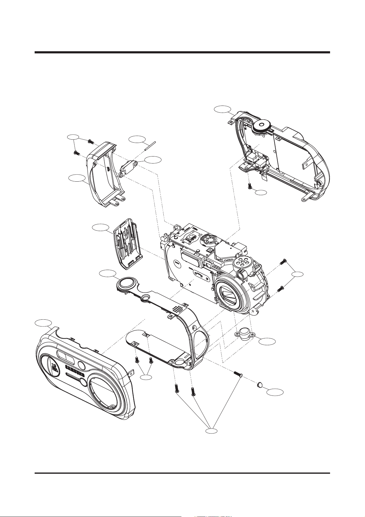
1. MAIN ASSEMBLY
1-9
1-2
1-4
1-7
1-3
1-6
1-5
1-8
1-18
1-1
1-10
1-8
1-11
1-12
Page 16

17
Ⅲ. EXPLODED VIEWS AND PARTS LIST
17
FFiigg..NNoo.. PPaarrttss NNoo.. PPaarrttss NNaammee QQ''ttyy RReemmaarrkkss
1-1 Q9007222201A FRONT COVER ASSY DIGIMAX A7 1
Q9007229901A FRONT COVER ASSY KENOX D7 1
1-2 Q6003044801A SCREW 2
1-3 Q7217349801A A7_COVER_CENTER 1
1-4 Q7217331701A D2 COVER SIDE MERCURY SILVER 1
1-5 Q7212184201A D2 RING STRAP MERCURY SILVER 1
1-6 Q7411115301A D2_RING_STRAP_PIN 1
1-7 Q9007219601A D2 COVER BATTERY MERCURY SILVER 1
1-8 Q6002004501A TAPPING_SCREW 4
1-9 Q9007222701A REAR COVER ASSY 1
1-10 Q6009002801A D2_TRIPOT_SCREW 1
1-11 Q7211077401A D2_COVER_CENTER-RUBBER 1
1-12 Q6002004701A SCREW 3
▶▶
PARTS LIST
Page 17
18
Ⅲ. EXPLODED VIEWS AND PARTS LIST
18
2. BODY COVER ASSEMBLY
2-31
2-30
2-1
2-9
2-7
2-32
2-1
2-10
2-34
2-14
2-13
2-12
2-1
2-1
2-5
2-3
2-2
2-29
2-6
2-4
2-28
2-6
2-27
2-8
2-18
2-19
2-25
2-11
2-24
2-15
2-16
2-17
2-26
2-22
2-20
2-21
2-23
2-33
Page 18

19
Ⅲ. EXPLODED VIEWS AND PARTS LIST
19
FFiigg..NNoo.. PPaarrttss NNoo.. PPaarrttss NNaammee QQ''ttyy RReemmaarrkkss
2-01 Q6002004601A SCREW 14
2-02 Q7211077501A D2_COVER_BATTERY_PIN 1
2-03 Q7211070201A BAT-GUIDE 1
2-04 Q6107056601A BAT-DOOR-SPRING 1
2-05 Q7011049501A D2_DOOR_SIDE_BTCN 1
2-06 Q7409172201A D2_CHASSIS_MYLAR 1
2-07 Q9008084001A STROBE BD ASSY 1
2-08 Q7409182801A A7_SPONGE_BTCN 2
2-09 Q9008084101A MAIN BD ASSY 1
2-10 Q7409182701A D2_LENS_FPC_TAPE 1
2-11 Q9003020801A FINDER ASS'Y 1
2-12 Q7409172801A CCD COPPER 1
2-13 Q9008084201A SMT ASSY -SENSOR BD 1
2-14 Q7012049601A CCD PLATE 1
2-15 Q0604005101A CCD SENSOR 1
2-16 Q6003046601A TAPPING_SCREW 3
2-17 Q9002130001A LENS ASSY 1
2-18 Q7011049701A SPEAKER 1
2-19 Q0902008601A MIC. 1
2-20 Q7308015201A FLASH-BAND 1
2-21 Q7409156201A INSULATING TAPE 1
2-22 Q7409182201A COPPER FOIL 1
2-23 Q0611004301A FLASH TUBE 1
2-24 Q7011052601A REFLECTOR 1
2-25 Q7217332001A D2_PANEL_FLASH 1
2-26 Q7409172001A D2_CHASSIS 1
2-27 Q9008084301A SMT ASSY -TRANSFER BD 1
2-28 Q7011049801A D2_CHASSIS_SIDE_BTCN 2
2-29 Q9008084401A POWER BD ASSY 1
2-30 Q7409172501A D2_MYLAR_SHUTTER 1
2-31 Q7409172601A D2_MYLAR_SHUTTER 1
2-32 Q7409172701A A7_PCB_MAIN_MYLAR 1
2-33 Q7409190201A D2_PCB_TRANSFER_MYLAR 1
2-34 Q9008084501A FPC-SENSOR ASM 1
▶▶
PARTS LIST
Page 19
20
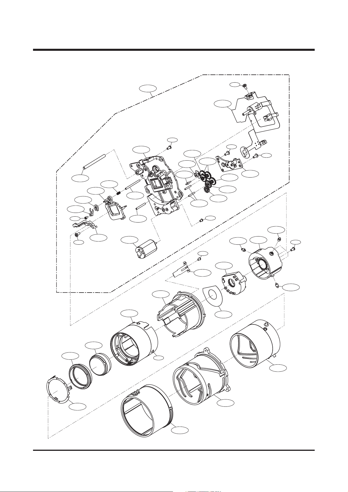
Ⅲ. EXPLODED VIEWS AND PARTS LIST
20
3. BARREL ASSEMBLY
3-23
3-25
3-19
3-5
3-24
3-22
3-26
3-21
3-8
3-3
3-4
3-2
3-1
3-43
3-10
3-6
3-14
3-7
3-15
3-33
3-9
3-18
3-11
3-13
3-12
3-17
3-20
3-32
3-16
3-28
3-17
3-32
3-30
3-36
3-38
3-37
3-35
3-29
3-34
3-32
3-27
3-31
3-39
3-40
3-41
3-42
Page 20

21
Ⅲ. EXPLODED VIEWS AND PARTS LIST
Fig.No. Parts No. Parts Name Q'ty Remarks
3-1 Q9002125201A LENS BASE ASS'Y 1
3-2 Q7212178705A LENS BASE 1
3-3 Q7411085401A AF GUIDER BAR_A 1
3-4 Q7411100601A AF GUIDE BAR 1
3-5 Q7411101001A FINDER GUIDE BAR 1
3-6 Q7411085902A ZOOM GEAR_A SHAFT 1
3-7 Q7411090001B ZOOM GEAR_C SHAFT 2
3-8 Q3107001701A ZOOM MOTOR 1
3-9 Q9611142007 SCREW 2
3-10 Q7212160001B ZOOM MOTOR GEAR 1
3-11 Q7411085802A ZOOM GEAR_D 1
3-12 Q7411085702A ZOOM GEAR_C 1
3-13 Q7411085601B ZOOM GEAR_B 1
3-14 Q7212160101A ZOOM GEAR_A 1
3-15 Q7212160602B ZOOM GEAR_E 2
3-16 Q7212178801A ZOOM COVER 1
3-17 Q0961900301A SCREW 3
3-18 Q9008068201A MAIN PCB ASS'Y 1
3-19 Q6003019201A SCREW 2
3-20 Q0994913101A SCREW 1
3-21 Q6107048305A 3RD LENS BARREL SPRING 1
3-22 Q9002124701A 3rd LENS ASS'Y 1
3-23 Q7012069406C AF LIMIT SPRING 1
3-24 Q7012069301A AF CLIP 1
3-25 Q6001014001A SCREW 1
3-26 Q7212178906A AF HOLDER 1
3-27 Q7212159302A GUIDE PLATE 1
3-28 Q9002124601A 2nd LENS ASS'Y 1
3-29 Q9005016301A SHUTTER ASS'Y 1
3-30 Q9761142507 SCREW 2
3-31 Q7409123201A SHUTTER PROTECT SHEET 1
3-32 Q7411085305A 2ND MOVE PIN 3
3-33 Q6001014001A SCREW 1
3-34 Q7012069202A F-PCB GUIDER 1
3-35 Q7212171301A ZOOM RING 1
3-36 Q7212158903A 1ST GUIDE BARREL 1
3-37 Q9002109201A 1st LENS ASSY 1
3-38 Q7012069004B 1ST PUSH PLATE 1
3-39 Q7411097502A 1st MOVE PIN 2
3-40 Q7212171201A CAM BARREL 1
3-41 Q7212178501A OUTER CAM BARREL 1
3-42 Q9002125101A OUTER GUIDE BARREL ASS'Y 1
3-43 Q0961900301A SCREW 5
21
▶▶
PARTS LIST
Page 21
22
Ⅲ. EXPLODED VIEWS AND PARTS LIST
22
4. BARRIEL ASSEMBLY
4-1
4-11
4-5
4-4
4-12
4-2
4-10
4-3
4-3
4-9
4-4
4-8
4-7
4-6
Page 22

23
Ⅲ. EXPLODED VIEWS AND PARTS LIST
23
FFiigg..NNoo.. PPaarrttss NNoo.. PPaarrttss NNaammee QQ''ttyy RReemmaarrkkss
4-1 Q9002113901A BARRIER ASS'Y 1
4-2 Q7212167704A NEW FRONT PANEL 1
4-3 Q6107051702A NEW CLOSE SPRING 2
4-4 Q7212160403B BARRIER_C 2
4-5 Q7212167804A NEW BARRIER_A 1
4-6 Q7212167902A NEW BARRIER_B 1
4-7 Q7012073502A NEW BARRIER BASE 1
4-8 Q7012073403A NEW LEVER_B 1
4-9 Q7411095501A NEW LEVER PIN 1
4-10 Q7012073301A NEW LEVER_A 1
4-11 Q6107051802A NEW OPEN SPRING 1
4-12 Q7409120802B FORNT PANEL TAPE 2
▶▶
PARTS LIST
Page 23
24
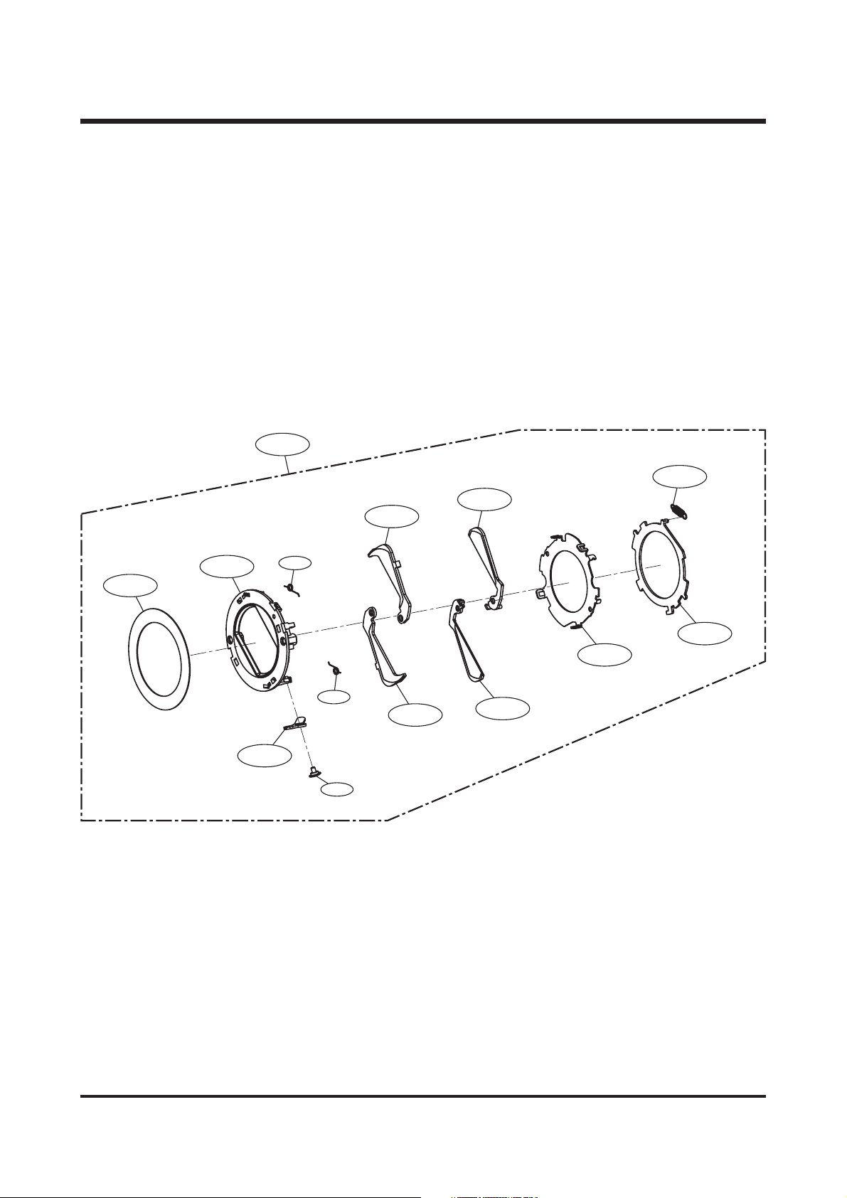
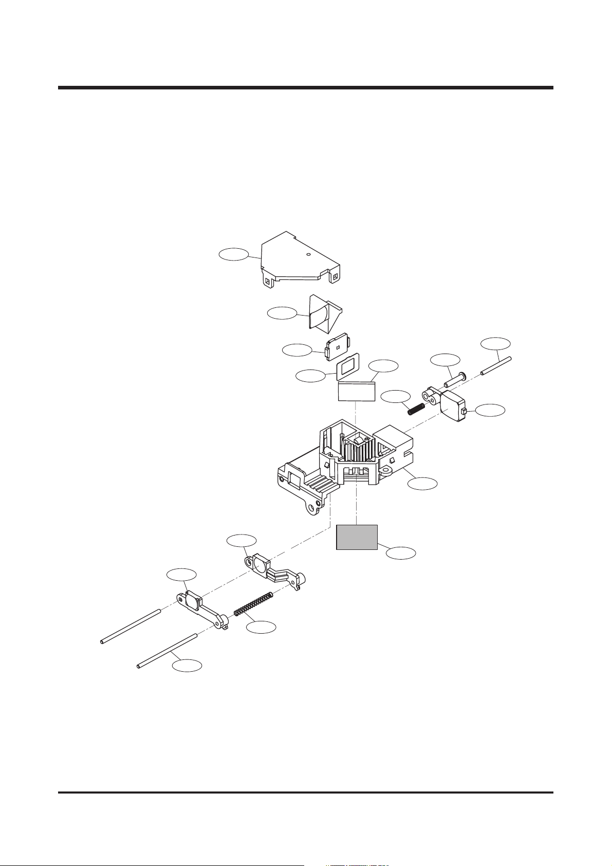
Ⅲ. EXPLODED VIEWS AND PARTS LIST
24
5. FINDER ASSEMBLY
5-15
5-11
5-4
5-6
5-5
5-13
5-14
5-12
5-7
5-10
5-8
5-9
5-2
5-1
5-3
Page 24

25
Ⅲ. EXPLODED VIEWS AND PARTS LIST
25
FFiigg..NNoo.. PPaarrttss NNoo.. PPaarrttss NNaammee QQ''ttyy RReemmaarrkkss
5-1 Q7409144002A SHIELD_A 1
5-2 Q7213034004A FINDER BASE 1
5-3 Q7411100801A FINDER SHAFT 2
5-4 Q6721009002A CO LENS 1
5-5 Q6107055002A FINDER SPRING 1
5-6 Q9003021101A VA LENS ASS'Y 1
5-7 Q7411100901A EP SHAFT 1
5-8 Q6107055101A EP SPRING 1
5-9 Q6721009302A EP LENS 1
5-10 Q6003040801A SCREW 1
5-11 Q6726002401A PORRO PRISM 1
5-12 Q6725001001B MIRROR 1
5-13 Q6721009202A TARGET LENS 1
5-14 Q7013015203A FINDER MASK 1
5-15 Q7213034104A FINDER COVER 1
▶▶
PARTS LIST
Page 25
26
Ⅲ. EXPLODED VIEWS AND PARTS LIST
26
6. FRONT COVER ASSEMBLY
6-
6-9
6-10
6-
6-11
6-6-13
6-
6-
6-12
6-
6-3
6-
6-4
6-5
6-
6-2
6-
6-14
6-6-8
6-
6-15
6-
6-
6-
6-1
6-6
6-
6-16
6-
6-7
Page 26

27
Ⅲ. EXPLODED VIEWS AND PARTS LIST
FFiigg..NNoo.. PPaarrttss NNoo.. PPaarrttss NNaammee QQ''ttyy RReemmaarrkkss
6-1 Q7411115401A D2_LENS_RING 1
6-2 Q7017040701A SAMSUNG-BADGE 1
6-3 Q7204022301A A7_GRIP_FRONT 1
6-4 Q7218007401A D2_MIRROR 1
6-5 Q7217332501A D2 FRONT DECORATION MERCURY SILVER 1
6-6 Q6002005101A SCREW-T-PLAT 1
6-7 Q7217332701A D2_GUIDE_SELFTIMER 1
6-8 Q7217349901A A7_COVER_FRONT 1
Q7217355801A D7_COVER_FRONT
6-9 Q7217333801A D2_KNOB_SHUTTER 1
6-10 Q6107060401A D2_SPRING_SHUTTER 1
6-11 Q7215059201A D2_SHUTTER_DECORATE_RING 1
6-12 Q7217349801A A7_COVER_CENTER 1
6-13 Q7217334001A D2 KNOB POWER MERCURY SILVER 1
6-14 Q7217334201A D2_VF_WINDOW 1
6-15 Q6002004601A SCREW-T-PLAT 1
6-16 Q7217350001A A7_SIDE_DECORATION 1
27
▶▶
PARTS LIST
Page 27
28
Ⅲ. EXPLODED VIEWS AND PARTS LIST
28
7. BACK COVER ASSEMBLY
7-8
7-9
7-23
7-5
7-25
7-24
7-7
7-1
7-6
7-17
7-18
7-4
7-1
7-19
7-21
7-3
7-13
7-2
7-15
7-10
7-11
7-12
7-14
7-20
7-26
7-27
7-16
7-22
7-1
7-1
Page 28

29
Ⅲ. EXPLODED VIEWS AND PARTS LIST
29
FFiigg..NNoo.. PPaarrttss NNoo.. PPaarrttss NNaammee QQ''ttyy RReemmaarrkkss
7-1 Q6002005101A SCREW-T-PLAT 5
7-2 Q7217340601A D2 KNOB FUNCTION PURE SILVER 1
7-3 Q7212184401A D2_GUIDE_VF_LED 2
7-4 Q7212184501A D2_GUIDE_MODE_DIAL_LED 1
7-5 Q7309044001A D2_KNOB_ZOOM_RUBBER 1
7-6 Q7017043101A D2_MODE_DIAL_PLATE 1
7-7 Q7217334901A D2_MODE_DIAL_SPACER 1
7-8 Q7212184601A D2_KNOB_ZOOM 1
7-9 Q7212184801A D2 KNOB MODE DIAL PURE SILVER 1
7-10 Q6107060501A D2_MODE_DIAL_SPRING 1
7-11 Q7213035501A D2_VIEW_FINDER_LENS 1
7-12 Q7217350201A A7_COVER_USB 1
7-13 Q7217350301A A7_COVER_REAR 1
7-14 Q7409182301A A7_SPONGE_LCD 1
7-15 Q0704011301A TFT LCD PANEL 1
7-16 Q7001004701A A7_LCD_PLATE 1
7-17 Q9010050001A USB/DC BD ASSY 1
7-18 Q7011049901A D2_PCB_USB_FIX_PLATE 1
7-19 Q6002005001A SCREW 6
7-20 Q7409182501A A7_LCD_SHIELD 1
7-21 Q7409172201A D2_CHASSIS_MYLAR 2
7-22 Q0809001901A D2_EMI 1
7-23 Q9007223001A FUNCTION ASM 1
7-24 Q9007223101A MODE DIAL ASM 1
7-25 Q9007223201A REAR COVER SUB ASM 1
7-26 Q9008084601A UI BD ASM 4
7-27 Q9007223301A LCD ASM 1
▶▶
PARTS LIST
Page 29
30
Ⅲ. EXPLODED VIEWS AND PARTS LIST
30
8. PACKING ITEM
8-9
8-12
8-10 8-13
8-17
8-1
8-14
8-16
8-18
8-15
8-11
8-5
8-6
8-7
8-2
8-3
8-4
8-8
Page 30

31
Ⅲ. EXPLODED VIEWS AND PARTS LIST
31
FFiigg..NNoo.. PPaarrttss NNoo.. PPaarrttss NNaammee QQ''ttyy RReemmaarrkkss
8-1 QP960210101A PE BAG (FOR CAMERA) 1
8-2 Q6909011601A PE BAG (FOR ACCESSORY) 1
8-3 Q6901176801A INNER PAD_D Digimax A5_A6_KOR/EXP 1
8-4 Q6904025601A POUCH_Digimax A5_A6(SAMSUNG) 1
8-5 Q6806251401A Q/GUIDE_KENOX D7_KOR 1
Q6806251501A Q/GUIDE_Digimax A7_ENG 1
Q6806251601A Q/GUIDE_Digimax A7_GER 1
Q6806251701A Q/GUIDE_Digimax A7_FRA 1
Q6806251801A Q/GUIDE_Digimax A7_SPA 1
Q6806251901A Q/GUIDE_Digimax A7_ITA 1
Q6806252001A Q/GUIDE_Digimax A7_TUR 1
Q6806252101A Q/GUIDE_Digimax A7_DUT 1
Q6806252201A Q/GUIDE_Digimax A7_POR 1
Q6806252301A Q/GUIDE_Digimax A7_SWE 1
Q6806252401A Q/GUIDE_Digimax A7_DEN 1
Q6806252501A Q/GUIDE_Digimax A7_FIN 1
Q6806252601A Q/GUIDE_Digimax A7_RUS 1
Q6806252701A Q/GUIDE_Digimax A7_CHI(S) 1
Q6806252801A Q/GUIDE_Digimax A7_CHI(T) 1
8-6 Q6806252901A U/MANUAL_KENOX D7_KOR 1
Q6806253001A U/MANUAL_Digimax A7_ENG 1
Q6806253101A U/MANUAL_Digimax A7_GER 1
Q6806253201A U/MANUAL_Digimax A7_FRA 1
Q6806253301A U/MANUAL_Digimax A7_SPA 1
Q6806253401A U/MANUAL_Digimax A7_ITA 1
Q6806253501A U/MANUAL_Digimax A7_TUR 1
Q6806253601A U/MANUAL_Digimax A7_DUT 1
Q6806253701A U/MANUAL_Digimax A7_POR 1
Q6806253801A U/MANUAL_Digimax A7_SWE 1
Q6806253901A U/MANUAL_Digimax A7_DEN 1
Q6806254001A U/MANUAL_Digimax A7_FIN 1
Q6806254101A U/MANUAL_Digimax A7_RUS 1
Q6806254201A U/MANUAL_Digimax A7_CHI(S) 1
Q6806254301A U/MANUAL_Digimax A7_CHI(T) 1
8-7 Q6807002601F WARRANTY CARD_KOREA 1
Q6807003003U WARRANTY CARD_EXP 1
Q6807010902B WARRANTY CARD_RUS(3 YEARS) 1
Q6807011301B WARRANTY CARD_TSOE(CHINA) 1
8-8 Q6901208001A G/T BOX_KENOX D7_KOR 1
Q6901208101A G/T BOX_Digimax A7_EXP/AUS 1
Q6901208201A G/T BOX_Digimax A7_USA/CAN 1
▶▶
PARTS LIST
Page 31

32
Ⅲ. EXPLODED VIEWS AND PARTS LIST
32
▶▶
PARTS LIST
FFiigg..NNoo.. PPaarrttss NNoo.. PPaarrttss NNaammee QQ''ttyy RReemmaarrkkss
8-9 Q7409145001A STRAP_DIGIMAX_UCA 3_KOR/EXP 1
8-10 Q3802003001A USB CABLE_A5_A6 1
8-11 Q4609010801A DRIVER + Digimax Viewer 2.1+ Arcsoft PI 4.0 1
8-12 Q7409183501A FCC LABEL_Digimax A7_EXP (MADE IN CHINA) 1
Q7409183601A FCC LABEL_Digimax A7_EXP (MADE BY SAMSUNG) 1
8-13 Q4602000601A SECURE DIGITAL CARD(32MB) 1
8-14 Q4301003101A "Ni-MH BATTERY SNB-2312 (1.2V, AA) - SAMSUNG" 1
8-15 Q4301003001A Ni-MH CHARGER SBC-N1 1
8-16 Q3801003001A AC CODE CABLE_KOR-D1 1
Q3801003201A AC CODE CABLE_EXP-D1 1
Q3801003101A AC CODE CABLE_USA-D1 1
Q3801001001A AC CODE CABLE_UK-DSC220SE 1
Q3801003401B AC CODE CABLE_AUS-D1 1
8-17 Q4301002801A LI-ION BATTERY SBP-1303(CR-V3 Li-ion Type) 1
8-18 Q4301002901A LI-ION CHARGER SBC-L1 1
Page 32

ⅣⅣ.. AADDJJUUSSTTMMEENNTT
333333333333
11.. DDiiggiittaall ccaammeerraa sseerrvviiccee
To take a digital camera service(Repair, Tuning and Checking), the following equipments have to be
arranged.
The sequences for the camera service are as shown
alongside.
1. Receiving the camera
When receiving a camera, check whether the accessories
are included or not and ask the customer exact problems.
2. Checking the camera
Checking the camera with priority given to the exact
problems to find overall malfunctions.
3. Repairing the camera
Repair the camera malfunctions found at the step 2.
4. Inspection
After repairing the camera, inspect all of the camera
functions.(See p.56)
※ The illustrations may be different from the real display in accordance with the camera model.
11.. CChheecckkiinngg tthhee ccaammeerraa aanndd
IInnssppeeccttiioonn
22.. RReeppaaiirriinngg tthhee ccaammeerraa 33.. TTuunniinngg
Receiving the camera
Checking the camera
Repairing the camera
Tuning
Inspection
Finish
Page 33

34
Ⅳ. ADJUSTMENT
3434343434
11)) EEqquuiippmmeennttss ffoorr cchheecckkiinngg aanndd iinnssppeeccttiioonn
To check and inspect the camera malfunction, the following equipments have to be arranged.
①①
②②
③③
⑤⑤
⑥⑥
⑦⑦
⑧⑧
⑪⑪
⑨⑨
⑩⑩
④④
No. Device Description
1 PC for inspection - Installing a digital camera driver or Checking the removable device
- Checking the file transference(upload and download)
- Playing back the still image or movie clip
2 HARD RACK, For the compatibility test.
by Operating System by the O/S(WIN 98SE, ME, 2000, XP)
3 Driver CD, by camera models S/W CDs for installing a camera driver
4 USB HUB For using all kinds of USB cable at a time
5 USB cable, by camera models For checking file transference(upload and download) by camera models
6 Chart for checking colors For checking color and image resolution before or after camera repair
7 TV MONITOR For checking video output and whether NTSC/PAL can be selected
8 Memory card by types For checking card recognition by brands and sizes
9 A/V CABLE For checking whether the image can be displayed on a external monitor
10 POWER SUPPLY For checking camera power by camera models
11 Power cable by camera models
Page 34

35
Ⅳ. ADJUSTMENT
3535353535
22)) EEqquuiippmmeennttss ffoorr ccaammeerraa rreeppaaiirr
To repair the camera, the following equipments have to be arranged.
①①
②②
③③
⑤⑤
⑥⑥
⑪⑪
⑨⑨
④④
⑩⑩
⑧⑧
⑪⑪
⑫⑫
⑬⑬
⑦⑦
No. Device Description
1 A set of tools Pincette/ Screwdriver/ Discharger etc.
2 Cleaning paper For cleaning camera lens and camera parts
3 Detergent container For containing detergent
4 Parts case For keeping various camera parts and disassembled camera parts
5 Anti-electricity mat For repairing table made from anti-electricity material
6 Soldering sponge For removing solder
7 Air pump For removing various kinds of dust
8 LIGHT BOX Color temperature 5100
9 POWER SUPPLY 7.5V 2.0A
10 Soldering iron Soldering iron that can select temperature
11 Tester Portable tester that can test AC/DC, Ω,♪ ect.
12 BATTERY & AC ADAPTOR & Rechargeable battery by camera models
AC ADAPTOR - SBP3603/ SBP3605/ SBP3606
- SLB 1437
- SBP 1103
Page 35

36
Ⅳ. ADJUSTMENT
3636363636
33)) EEqquuiippmmeennttss ffoorr ccaammeerraa ttuunniinngg
To tune the camera, the following equipments have to be arranged.
①①
②②
③③
⑤⑤
⑥⑥
④④
No. Device Description
1 AE TESTER For tuning AE and STROBE
2 AWB LIGHT For checking and tuning AWB
SOURCE BOX
3 COLOR chart For checking AWB and color of images
4 AF chart For tuning AF
5 Chart for checking For checking image resolution
resolution
6 TRIPOD
Page 36

37
Ⅳ. ADJUSTMENT
3737373737
44)) CChheecckk lliisstt ffoorr DDiiggiittaall ccaammeerraa rreeppaaiirr
To check the digital camera functions before/after repairing, refer to the check list.
NNoo.. CChheecckkiinngg iitteemm CChheecckk ppooiinntt
1 - Check the scratch, stain, misprint.
- Check whether the screws are turned firmly.
- Check the corrosion of terminal, bad exterior.
- Do chemical and glue test to the printing/ painting parts.
2 - Check the connecting and contact condition.
3 - Insert the batteries with the correct polarity and check the
contact condition.
- Check whether the cover is opened easily after closing.
4 - The card can be inserted or removed easily and cover is
closed firmly.
- Do inserting and removing card(SD/MMC) test two times.
→ The card must be inserted firmly and has not to spring out.
- Insert the card/batteries and give a little impact on the
camera. The camera must recognize the card and “CARD
LOCKED”message has not to be displayed.
5 - When the cable is inserted, check whether the images play
back on the external monitor.
6 - Check whether the green LED is blinking, SAMSUNG LOGO is
on and the start-up sound sounds.
- Check the “L”and “FINE”icon on the LCD monitor.
- Check whether the AE function is correct at the low light and
high light condition.
- Check whether the “beep”sounds on the recording and movie
clip mode.
→ The “beep”can be sounded in the microphone part. Check
that in a quiet room.
7 - Press the zoom W/T button with the viewfinder.
→ Check dust and percentage of the frame seen, zoom rate.
- Press the zoom W/T button with the TFT-LCD monitor.
→ Check the zoom rate and whether the zoom bar moves
smoothly.
8 - Check whether the Macro icon(Flower) is displayed on the
LCD monitor.
- Check the AF in the Macro focus with the TFT-LCD monitor.
9 - Check whether the subject captured from 2M has over or
under exposure and the fucus is clear.
Check the exterior of a camera.
Insert the adapter.
Check the battery cover.
Check the card condition after
inserting the card.
Insert the Video cable.
Turn on the camera.
Press the zoom W/T button.
Macro focus.
Normal focus.
Page 37

38
Ⅳ. ADJUSTMENT
3838383838
NNoo.. CChheecckk iitteemm CChheecckk ppooiinntt
10 - Check whether the icon and counter are displayed on the
LCD monitor.
11 - Check whether the recording time is displayed and there
are a noise, dim frame and discontinuous frame in the movie
clip.
12 - Check whether the zoom rate is changed and there are
unclear part, noise and dim part in the image.
- The distance from the subject is 2M and have to use the
FILL IN flash.
13 - Check whether the PLAY mode can be selected without any
problem and there are any noise, frame shaking and
discoutinuous frame.
- Check the voice recorded in the still image and the movie clip.
- Check whether the still image can be enlarged correctly
with the 5 function button.
14 - Select 2 sec. of slide show interval time and check whether
there are any noise, image shaking and discontinuous frame.
15 - Check whether the mode dial is rotated with the equal force.
- Check whether each camera mode can be recognized correctly.
16 - Check whether there are unclear part, dim part, noticeable
flare, noise, ghost image and smear.
17 - Check whether all images are deleted.
18 - Check whether the “NO IMAGE”message is displayed on the
LCD monitor.
- Check whether the LARGE, FINE icon and 0018 number are
displayed.
- Check whether the camera power is turned off without any
problem.
MANUAL focus.
Take a movie clip with
TELE zoom during 10 seconds.
Take a chart with TELE zoom
in a low light condition.
Play back a image with
the TFT LCD monitor.
Start the slide show
in the PLAY mode.
Try to rotate the mode dial.
Download a image from a PC
with USB cable and check the
image quality in a external
monitor.
Format the card in the PLAY
mode.(Delete all images in the
PLAY mode)
Check whether there is no image
and reset the camera. Remove
the card and turn off the camera.
Page 38

39
Ⅳ. ADJUSTMENT
3939393939
22.. HHooww ttoo cchheecckk tthhee FFIIRRMMWWAARREE VVEERRSSIIOONN
1. Remove the SD card from camera. 2. Change the Mode dial to the Voice record.
3. Press the Power on button while pressing 4. Check the Firmware version
the OK button.
5. To turn ofr the camera, press the Power button.
Page 39

40
Ⅳ. ADJUSTMENT
4040404040
33.. HHooww ttoo uuppddaattee tthhee FFIIRRMMWWAARREE UUPPGGRRAADDEE
1. Connect the service site ‘www.samsungcamera.com/service’and click the Support center menu on
the left side menu.
2. Select the model and category.
Page 40

41
Ⅳ. ADJUSTMENT
4141414141
3. Download the sa7m.elf to the windows directory and copy to the removable
disk after connecting the camera. (Do not use card Reader)
Caution ) Format the SD card using the camera
After copying the file, check the file name.
4. Insert the SD card that has the firmware. 5. Change the Mode dial to the Voice record.
Page 41

42
Ⅳ. ADJUSTMENT
4242424242
6. When the update is progress, the red light of
5. Turn on the power while preesing the Wide Flash LED is blinking. If the blinking stops
button. after few minutes, the update is done and
remove the battery to power off.
7. If your turn on the camera after removing the
Card, ‘Media error’message and ‘set’is
shown like below image. Select YES then, 9. Check the firmware whether it is updated
‘Format Done’message is shown and the or not.
camera shows the Voice record mode.
※※ WWhheenn yyoouu ddoo tthhee FFiirrmmwwaarree uuppggrraaddee,, yyoouu hhaavvee ttoo uussee tthhee AACC AAddaappttoorr.. IIff tthhee ccaammeerraa ttuurrnnss ooffff
wwhhiillee uuppddaattiinngg,, tthhee ccaammeerraa ccaannnnoott wwoorrkk.. AAfftteerr uuppddaattiinngg ffiirrmmwwaarree,, yyoouu hhaavvee ttoo rreesseett tthhee ccaammeerraa..
Page 42

43
Ⅳ. ADJUSTMENT
434343434343
44.. AADDJJUUSSTTMMEENNTT
11)) TTuunniinngg iitteemmss bbyy cchhaannggiinngg ppaarrttss
After changing the electronic parts of Digimax A5/A6the parts have to be tuned in accordnce with the
tuned items. The items listed on the table have to be tuned after change..
※This marked adjustment needs Xenon Short Arc Lamp to adjust. If there is at least one of this
adjustment needed, please use EEPROM Read/Wirte which is shown on the next page.
22)) EEqquuiippmmeennttss ffoorr aaddjjuussttiinngg
▶ Equipments
- AE TESTER : XENON LAMP - LV 10, 13 and Halogen LAMP : LV 15
- LIGHT BOX : 5500。K
▶ Chart
- Focus chart : “AF CHART.pdf ”
- Gray Chart : 18% Reflector paper
33)) TTEESSTT MMOODDEE
a. Change the Mode dial to Voice record mode. b. Press the POWER ON button while pressing
OK button for about 3 sec. and the TEST
MODE is shown.
MAIN POWER BARREL CCD STROBE UI JACK
PCB PCB ASS’Y F PCB PCB F CPB PCB
FIRMWARE UP ● ● ● ● ●
FOCUS Clbt. ● ● ●
OB Clbt. ● ● ●
WB/AGC Clbt.※ ● ● ●
MESHUT 26 Clbt.※ ● ● ●
MESHUT 80 Clbt.※ ● ● ●
LIGHT/SLOW Clbt. ● ● ● ●
DARK DPC Clbt. ● ● ● ●
FLASH WB Clbt. ● ● ● ●
MB/LCD CHECK ● ● ● ● ● ● ●
KEY TEST ● ● ● ● ● ● ●
LCD OFFET ● ●
Page 43

44
Ⅳ. ADJUSTMENT
444444
c. When the TEST MODE execute, the adjustment d. Select No (Not OK) and then press OK button
of MB/LCD is shown like below. to change the adjustment page.
e. The adjustment for each step is shown like below.
<The adjustment is completed> <The adjustment is needed>
※ If you want to readjust menus that completed adjustment, select the menu that you wand push the
LCD button then you can see the like below.
a. The menu that is complete the adjustment b. To do the adjustment, press right button for
shows "Disable 001" change to "Disable 000"
444444
Page 44

45
Ⅳ. ADJUSTMENT
454545454545
44)) FFOOCCUUSS CCllbbtt..
<How to adjut>
a. Set the SF CHART.
b. Put the camera on tri-pod.
c. Put the camera 2m away from the chart.
d. Choose the FOCUS CLBT. in test mode and press OK button.
e. The adjutment will be automatically done and after adjustment, the camera will be shut off
automatically.
※ If the adjustment is failed and show the NG, please do the adjustment again.
<Select the FOCUS ADJUSTMENT> <Choose the OK and press OK button.>
<The adjustment is completed> <The adjustment is failed.>
AF Chart
2m
Camera
Tripod
Page 45

46
Ⅳ. ADJUSTMENT
464646464646
55)) OOBB CCllbbtt..
<How th adjust>
a. Enter the TEST MODE.
b. Block the LENS with black object to shut down the light.
c. Select the OB Clbt. and press the OK button then the adjustment will be done automatically.
※ If you fail the adjustment, the NG is shown and do the adjustment again.
<Select the OB Clbt> <Choose the OK and press OK button>
<Do the adjustment> <The adjustment is completed>
Page 46

47
Ⅳ. ADJUSTMENT
47474747474747
66)) LLiigghhtt//SSllooww((LLiigghhtt DDeeaadd PPiixxeell//SSllooww SShhuutttteerr DDeeaadd ppiixxeell CCaalliibb..))
<How to adjus>
a. Enter the TEST MODE
b. Select the Light/Slow. c. Select OK and press the OK button.
d. The adjustment is executed. e. The adjustment is completed.
f. When the Light/Slow adjustment is completed, the Burring will be executed.
g. When the Burring is completed, OK sign will be shown.. (about 40 Min)
Page 47

48
Ⅳ. ADJUSTMENT
48484848484848
77)) DDaarrkk DDPPCC ((DDaarrkk DDeeaadd PPiixxeell CCaalliibb..))
Equipment> LV10, K=1.3, (Halogen Lamp)
<How to adjus>
a. Enter the TEST MODE.
b. Set the LIGHT SOURCE BOX to LV 10 and K=1.3.
(Halogen Lamp has to be used.)
c. Select the Dark DPC. d. Select OK and press the OK button
e. The adjustment is executed. f. The adjustment is completed.
※ If the adjustment is failed, the NG sign will be shown. In this case, adjust the camera again.
Light source box
Camera
Page 48

49
Ⅳ. ADJUSTMENT
49494949494949
88)) FFllaasshh WWBB
Equipment> Dark room, Gray Chart (18%)
<How to adjus>
a. Enter the TEST MODE.
b. Set the 18% Reflector paper in the dark room and put the camera 1m away from the chart.
c. Select the Flah WB. d. Select OK and press the OK button.
e. The adjustment is executed. f. The adjustment is completed.
※ If the adjustment is failed, the NG sign will be shown. In this case, adjust the camera again.
Reflector paper
1m
Camera
Tripod
Page 49

50
Ⅳ. ADJUSTMENT
505050
99)) MMBB//LLCCBB
This mode tests the MAIN BOARD like below section..
. FW Version, RTC Check, AGC Check, E-Shutter Check, SD Card Check, Charge/Trigger,
Record/Play Audio, LCD check
a. Enter the TEST MODE.
b. Select the MB/LCD. c. Select OK and press the OK button
d. The adjustment for each section is executed. e. The adjustment is completed..
5050
Page 50

51
Ⅳ. ADJUSTMENT
515151
1100)) KKEEYY TTEESSTT
This mode tests the working statement for each KEY.
a. Enter the TEST MODE..
b. Select the KEY TEST. c. Select OK and press the OK then press the
each button or rotate it. The section will be
chaged to green if it acts properly.
1111)) LLCCDD OOFFFFSSEETT
This mode adjust the clearance of OSD.
a. Enter the TEST MODE.
b. Select the KEY TEST. c. Adjust the OSD clearance by using Left and
Right button. At the middle of top area, there
is that status mark which is shown the currant
state.
Page 51

52
Ⅳ. ADJUSTMENT
55.. EEEEPPRROOMM DDaattaa RReeaadd//WWrriittee
⇨ After replacing the Main Board, some adjustments cannot be done. In this case,
use this method.
⇨ After using this method, please test the function and capability of the camera to
check that the camera works fine.
⇨
When using this program, make sure that the USB cable which is only for R/W EEPRom sould be
used to connect the camera with PC.
1. Program : EepromTool.ZIP
2. How to use : Download the program in temporary folder.
The uploading location : http://www.samsungcamera.com/service
DDoouubbllee CClliicckk!!
Page 52

53
Ⅳ. ADJUSTMENT
3. Extract the downloaded program.
CClliicckk tthhee [[BBrroowwssee]] bbuuttttoonn!!
CClliicckk tthhee [[EExxttrraacctt]] bbuuttttoonn!!
Page 53

54
Ⅳ. ADJUSTMENT
=> Save it in the temporary folder.
4. Execute the EepromTool.exe in the EEPROM Folder which is created after extracting.
CClliicckk tthhee [[OOKK]] bbuuttttoonn!!
Page 54

55
Ⅳ. ADJUSTMENT
=> The main screen in EepromTool program.
5. Connect the camera with PC by using USB cable.
The camera should be connected in the TEST MODE. => How to enter the TEST MODE : Turn on the
power while pressing MENU KEY in the Voice Recoding Mode.
①①
②②
③③
Page 55

56
Ⅳ. ADJUSTMENT
CClliicckk tthhee [[CCoonnttiinnuuee AAnnyywwaayy]] bbuuttttoonn!!
CClliicckk tthhee [[NNEEXXTT]] bbuuttttoonn!!
6. When you install the USB Driver, use the Driver which is included in Eeprom Tool program for TEST
MODE.
CClliicckk tthhee [[OOKK]] bbuuttttoonn!!
Page 56

57
Ⅳ. ADJUSTMENT
7. When the camera is recognized, click the [Read From Camera].
=> The data are shown which is readed from camera.
CClliicckk tthhee [[RReeaadd FFrroomm CCaammeerraa]] bbuuttttoonn!!
Page 57

58
Ⅳ. ADJUSTMENT
9. After saving, release the connection.
10. Connect the repaired camera(which doesn’t adjust) with PC.
In this case, the camera should be connected in TEST MODE.
TEST MODE Driver doesn’t need to reinstall.
TTyyppee tthhee FFiillee nnaammee,, CClliicckk tthhee [[SSaavvee]] bbuuttttoonn!!
8. Click the [write File] button to save the data from camera in the temporary folder.
CClliicckk tthhee [[WWrriittee]] bbuuttttoonn!!
Page 58

59
Ⅳ. ADJUSTMENT
CClliicckk tthhee [[RReeaadd FFiillee]] bbuuttttoonn!!
FFiinnee tthhee ffiillee wwhhiicchh yyoouu wwaanntt ttoo rreeaadd aanndd CClliicckk tthhee [[OOPPEENN]] bbuuttttoonn!!
11. After camera connects with PC, read the file which is saved before.
Page 59

60
Ⅳ. ADJUSTMENT
12. Click the [Write To Camera].
CClliicckk tthhee [[WWrriittee ttoo CCaammeerraa]] bbuuttttoonn!!
Page 60

61
Ⅳ. ADJUSTMENT
13. When the [Write eep Data to Camera OK!!!] Message is shown at the state bar under the
window, release connection between camera and PC.
14. After copying the EEPROM DATA , basic test of camera function and capability of camera
SHOULD BE DONE before sending to customer.
Page 61

6262
ⅤⅤ.. PPAATTTTEERRNN DDIIAAGGRRAAMM
62626262626262
11.. PPAARRTTSS AARRRRAANNGGEEMMEENNTT FFOORR EEAACCHH PPCCBB AASSSS''YY
1) MAIN PCB ASSEMBLY_TOP
Page 62

636363
Ⅴ. PATTERN DIAGRAM
636363636363
2) MAIN PCB ASSEMBLY_BOTTOM
Page 63

646464
Ⅴ. PATTERN DIAGRAM
646464646464
3) POWER PCB ASSEMBLY_TOP
Page 64

656565
Ⅴ. PATTERN DIAGRAM
656565656565
4) POWER PCB ASSEMBLY_BOTTOM
Page 65

66666666666666
Ⅴ. PATTERN DIAGRAM
6666
5) SENSOR PCB ASSEMBLY_TOP
Page 66

67676767676767
Ⅴ. PATTERN DIAGRAM
6767
6) SENSOR PCB ASSEMBLY_BOTTOM
Page 67

68686868686868
Ⅴ. PATTERN DIAGRAM
6868
7) STROBE PCB ASSEMBLY_TOP
Page 68

69696969696969
Ⅴ. PATTERN DIAGRAM
6969
8) STROBE PCB ASSEMBLY_BOTTOM
Page 69

70707070707070
Ⅴ. PATTERN DIAGRAM
7070
9) USBDC PCB ASSEMBLY_TOP
Page 70

71717171717171
Ⅴ. PATTERN DIAGRAM
7171
10) USBDC PCB ASSEMBLY_BOTTOM
Page 71

72727272727272
Ⅴ. PATTERN DIAGRAM
7272
11) TRANSFER PCB ASSEMBLY
Page 72

73737373737373
Ⅴ. PATTERN DIAGRAM
7373
12) UI PCB ASSEMBLY
Page 73

7474
ⅥⅥ.. CCIIRRCCUUIITT DDIIAAGGRRAAMM
7474747474747474747474
11.. BBLLOOCCKK DDIIAAGGRRAAMM
CCD
SONY 7M
ICX489AQF
STROBE
AT1453
POWER
STROBE
IF
GPIO SENSOR
TG/VD/AFE
CXD4801GA
LENS
LENS
DRIVER
GPIO
M50234HP
IF
DISPLAY
LCD
TOPPOLY
TC020THEA7
LENS
DRIVER
TPG018A
DAC
GPIO
UI
32.768KHz
POWER
RTC
SDRAM IF
SDRAM 32M
FLASH IF
NAND
FLASH
COACH 6M
32M
USB IF
STORAGE IF
SD
USB
AUDIO IF
MIC SPEAKER
Page 74

75
Ⅵ. CIRCUIT DIAGRAM
75757575757575757575757575
22.. CCIIRRCCUUIITT DDIIAAGGRRAAMM
1-1) ZORAN COACH-6M
ADC1
TELE
WIDE
LED_RED
LED_GREEN
LED_GREEN
LED_RED
RESET
BAT LOW
RESET
ADC1
L ADC2
ADC0
MD0
MD1
MD2
MD3
MD4
MD5
MD6
MD7
MD8
MD9
MD10
MD11
MD12
MD13
MD14
MD15
UDQM
LDQM
SDCS
SDWE
SDCKE
MOTOR
_SH+
ZOOM_CW
MOTOR_SH-ZOOM_CCW
USBIO
UI_STROBE
PLAYBACK
MA0
MA1
MA2
MA3
MA4
MA5
MA6
MA7
MA8
MA9
MA10
MA11
MA12
MA13
MA14
FOCUS_BP
FOCUS_BN
FOCUS_AP
FOCUS_AN
FOCUS_HP
ZOOM_HP
ZOOM_CLK
PWR_ON
PWRENB
FLASH_CHARGE
FLASH_READY
FLASH_TRIG
SDCLK
SDCAS
SDRAS
RESET
BAT_PWR
GND_D
GND_D
3V3ASIC
3V3ASIC
3V3ASIC
GND_D
GND_D
GND_D GND_D
3V3ASIC
GND_D
GND_D
GND_D
GND_D
BAT_PWR
GND_D
3V3ASIC
GND_D
GND_A
GND_D
GND_A GND_A
GND_A
GND_A
GND_D
GND_D
H2
TP
1
.
J1
BL114-10RL
123456789
10
C13
NC
0402
R3
1.5K-J
0402
D2
LT
ST-S270KRKT
12
R25 47R 0402
C16
12pF/50V
0402 NPO-J
C15
12pF/50V
0402 NPO-J
C6
0.1uF/16V
0402 Y5V-Z
H3
TP
1
.
R17 33K-J
0402
R21 0R-J
0402
R26 1M
0402
P2
G
D
S
Q1
AO3413
SOT-23
1
2 3
Q3
DTC114YEA
SC75AA
1
3 2
C7
10uF/6.3V
0805 X
5R-M
EJTAG
UART
USB
ADC
GPIO
SDRAM
SPEAKER
GLOBAL
MIC
PWR
MOTOR
COACH-6M
U1A
B9A9B8
A8
D12
C12
A13
B13
A12
A11
P17
R16
U17
U16
U15
U14
U13
U12
T11
T12
T13
T14
T15
T16
T17
R17
U8
U9
T9
T10
U11U7U10
T8
U3U2U1R1R2T1T2T3T4T5U4T6T7U6U5
B3A3D5C5B4A4P10P9R9
R10
B2B1A2
A1
R12
R13
P12
P13
P2
P1
C8
C7
A6
A7
D7
D8
A17
B17B5A5
R8
B14
A16
A14
C14
N4N3P15
P16
GPADC0
GPADC1
GPADC2
GPADC3
VCM
AREF
MIC
MICENB
SPKRP
SPKRN
RAMDAT0
RAMDAT1
RAMDAT2
RAMDAT3
RAMDAT4
RAMDAT5
RAMDAT6
RAMDAT7
RAMDAT8
RAMDAT9
RAMDAT10
RAMDAT11
RAMDAT12
RAMDAT13
RAMDAT14
RAMDAT15
RAMRAS
RAMCAS
RAMCLK
RAMDQMH
RAMDQML
RAMCS
RAMWE
RAMCKEN
RAMADD0
RAMADD1
RAMADD2
RAMADD3
RAMADD4
RAMADD5
RAMADD6
RAMADD7
RAMADD8
RAMADD9
RAMADD10
RAMADD11
RAMADD12
RAMADD13
RAMADD14
PWM0
PWM1
PWM2
PWM3
PWM4
PWM5
XLGPIO0
XLGPIO1
XLGPIO2
XLGPIO3
M1D
M1C
M1B
M1A
EJTD1
EJTMS
EJTCK
EJTDO
RXD
TXD
USBDETECT
USBPUP
USBDM
USBDP
USBPDWN
USBID
RTCXO
RTCXI
VCLKI
VCLKO
TESTMODE
PWRON
PWRENB
RESET
PDETECT
SCL
SDA
FPDIN
FLSHTRIG
C2
0.1uF/16V
0402 Y5V-Z
RN2
22R
13456
78
2
H5
TP
1
.
C9
10uF/6.3V
0805 X
5R-M
P3
C18
22pF/50V
0402 NPO-J
C66
0.01uF/16V
0402 Y5V-Z
R12 33K-J
0402
P5
R24 NC
0402
R13
330R
0402
R20 22R-J
0402
R4
0R-J
0402
RN1
22R
13456
78
2
SW1
MITSUMI_SOT-152HST
SW-4
1 3
42
AC
D
B
R15 33K-J
0402
R10
33K
0402
SW2
MITSUMI_SOT-152HST
SW-4
1 3
42
AC
D
B
C65
0.01uF/16V
0402 Y5V-Z
P6
J7
PAD TO SPK
J100-2SA
1
2
C3
10uF/6.3V
0805 X
5R-M
L1 0R
0805
R14
2K
0402
R9 68R-J
0402
R11
33K
0402
R18 2.71M-F
0402
Y2
13.5MHz
XTAL
\5X3.2
1 2
C92 180pF/50V
0402 NPO-J
J6
PAD TO MIC
J100\2S
1
2
R19 1.5K
0402
C121
#22pF/50V
0402
C10
0.1uF/16V
0402 Y5V-Z
RN3
22R
13456
78
2
R23 NC
0402
U2
XC61CN2702MR
SOT-23
3
21
GND
IN OUT
TP19
1
.
C12 0.1uF/16V
0402 Y5V-Z Q2
DTC114YEA
SC75AA
1
3 2
C1
4.7uF/6.3V
0603 Y5V-Z
C5
0.1uF/16V
0402 Y5V-Z
R6
100K
0402
P4
Y1
32.768KHz
XT
AL-S
12
C14
NC
0402
C8
0.1uF/16V
0402 Y5V-Z
R1 7.5K
0402
R2
1M-J
0402
TP17
R16
665K-F
0402
RN4
22R
13456
78
2
H1
TP
1
.
C11
0.1uF/16V
0402 Y5V-Z
P1
D1
LTST-S270
KGKT
12
R22 22R-J 0402
TP1
8
C17
22pF/50V
0402 NPO-J
C63
NC
1206 X
5R-M
TP20
1
.
C4
0.047uF/16V
0402 X7R-K
C64
0.01uF/16V
0402 Y5V-Z
Page 75

76
Ⅵ. CIRCUIT DIAGRAM
76767676767676767676767676
1-2) ZORAN COACH-6M
PWR_DET
R27
33K
0402
3V3ASIC
T
BAT_ON
TG_RS
0402
0402
R34 0R-J
R5 NC
3V3ASIC
SW_CHARGE SW_DUTY
NF_D7
NF_D6
NF_D5
NF_D4
NF_D3
NF_D2
NF_D1
C1D1E1F1G1H1J1
FD7
FD6
FD5
FD4
FD3
FD2
FD1
P7
D3
NF_D0
K1
FD0
PWR_ON_P
2
1
R30
33K
R29
33K
R28
33K
SD_DET
SD_CS
J2C2E2
FCD
FEXTCE1
3
0402
0402
0402
SD_CLK
FCLK
GND_D
0402
C19 NC
DAN202U
SD_WP
F2G2H2
E3
FEXTBSY
SOT323
D4
1
C20
PWR_ON
NF_RB
NF_RE
NF_CE
FOE
FRESCE
FRESBSY
GND_D
PLAYBACK
0402
C21 NC
2
DAN202U
3
0.1uF/16V
0402 Y5V-Z
NF_WE
L
DCIN_DET
BAT_LOW_CTR
N2
N1
K2
FWR
FEXTCE2
FEXTRST
PLAYBACK_DET
SOT323
R31
33K
GND_D
0402
0402
R32 0R-J
M16
HIS
0402
R33 0R-J
M17
VIS
OFDCHDVD
AFE_CS
M15
N15
AFEVAL
SUBCNTL
3V3ASIC
PCNTL
EX
2XCK
0402
R36 NC
M14
L17
EXPCNTL
CCLKOUT
1XCK
L16
CCLK
3V3ASIC
GND_D
0402
C126 NC
AFE_SCK
AFE_SDATA
N16
N17
N14
SPCLK
SPDATA
BD9
TG_CS
TGVAL
0R
0603
C28
+
C27
C26
C25
C24
C23
C22
R3R4R5
VDDP1
10uF/10V
TC\A
0.1uF/16V
0402 Y5V-Z
0.1uF/16V
0402 Y5V-Z
0.1uF/16V
0402 Y5V-Z
0402 Y5V-Z
0.1uF/16V
0402 Y5V-Z
0.1uF/16V
0402 Y5V-Z
0.1uF/16V
R14
VDDP2
VDDP3
GND_D
3V3ASIC
BD10
R15P3P4P5P14
VDDP4
VDDP5
VDDP6
VDDP7
0402
BLM15AG221SN1
C122
0.1uF/16V
D14
D15C6C15B7D11D9B11
VDDP8
VDDP9
VDDP10
VDDP11
VDD
3V3ASIC
3V3ASIC
0402 Y5V-Z
BAT_PWR
0402
R41 0R
VDDP12
VDDP13
VDDUSB
BD11
BD12
GND_D
VDDDAC
VDDADC
0R
0603
C30
1uF/16V
0402
BLM15AG221SN1
C60
10uF/6.3V
C29
0.1uF/16V
0402
R42 22R
D13
A15
B16
D10
VDDRTC
VDDAUD
VDDPWR
VDDSPKR
0603 Y5V-Z
5R-M
0805 X
0402 Y5V-Z
H14F4D6
VDDPLL
VDDCORE1
VDDCORE2
GND_D
GND_A
0.2F/3.3V
C31
GCAP
+
P8
VDDCORE4
VDDCORE3
1V8ASIC
BD13
SLOAD
VSYNC
GND_D
R123 68R 0402
F17
G14
DVCNTL0
DVCNTL1
HSYNC
0402
R124 68R
G15
0603
BLM18PG300SN1
10uF/10V
C32
TC\A
+
C35
0.1uF/16V
0402 Y5V-Z
C34
0.1uF/16V
0402 Y5V-Z
C33
0.1uF/16V
0402 Y5V-Z
SCLK
SDATA
PLAYBACK_DET
PWR_DET
PWR_3V3_OFF
G16
G17
H17
H16
H15
DVCNTL2
DVCNTL3
DVCNTL4
DVCNTL5
DVCNTL6
DVCNTL7
DCLK
R43 47R-J
F16
DVCLK
0402
TP6
A10
GND_D
C36
C11
RSET
CVBS
NC
0402
GND_D
R44
392R-F
0402
GND_D
COACH-6M
U1B
M2
1234567891011
J2
123456789
0402
C139
NC
GND_D
PWR_ON_P
UI_STROBE
PWR_ON_P
FA2
FA1
FA0
M3
M4
M1
LED_TOP
SW_CHARGE
NF_CLE
NF_ALE
ADC0
FLASH_CHARGE
ADC2
ADC0
ADC2
UI_STROBE
FA3
FA4
FA5
FA6
FA7
FA8
L1L2L3
L4
K3
LED_FRONT4
LED_FRONT3
LED_FRONT2
LED_FRONT1
LED_FRONT5
101112
LED_TOP
GND_D
FLASH_READY
FLASH_TRIG
SW_DUTY
FLASH_TRIG
FLASH_READY
FLASH_CHARGE
STORAGE
FA9
FA10
FA11
FA12
FA13
J3
J4
K4
H3
H4
PWR_AGC
PWR_CCD
PWR_BL
PWR_LCD
LED_FRONT6
12
ZIV-12R3-B-0
0402
C138
0.01uF
0402
C137
0.01uF
3V3ASIC
3 2
LCD5V
FA14
FA15
FA16
F3
G3
G4
PWR_LENS
FOCUS_LED
ZOOM_LED
GND_D
SC75AA
Q4
DTA114YE
FA17
FA18
E4
D2D3D4
IRIS_BN
IRIS_BP
FA19
IRIS_AN
1
FA20
IRIS_AP
Q5
DTC114YEA
EXPCNTL
SC75AA
1
VID9
L14
RGB9
VID8
L15
RGB8
VID7
K14
K15
RGB7
3 2
SENSOR
VID6
VID5
VID4
VID3
VID2
J14
J15
K16
K17
RGB6
RGB5
RGB4
RGB3
RGB2
GND_D
5960
59
60
JS1
GND_D
BL+
J16
5758
BL-
VID1
J17
RGB1
5556
5758
GND_D
VID0
RGB0
5354
5354
5556
LCD8V5
5152
5152
GNDP1
R6
SD_WP
SD_DET
SD_WP
SD_DET
4748
4950
4748
4950
LCD5V
D3V3
C140
GNDP2
GNDP3
R7
R11
SD_CS
SD_CLK
SD_CLK
SD_CS
4344
4546
4344
4546
0402
0.01uF
GNDP4
GNDP5
K8
K9
K10
NF_D3
NF_D2
NF_D3
NF_D2
NF_D1
3738
3940
4142
3940
4142
CCD_15V
CCD_-7V5
GNDP6
GNDP7
P6
P7
NF_D0
NF_D1
NF_D0
PWR_LENS
3334
3536
3536
3738
GND
GNDP8
GNDP9
GNDP10
GNDP11
P11
E14
E15
PWR_CCD
PWR_BL
PWR_LENS
PWR_LCD
PWR_BL
PWR_LCD
PWR_CCD
2728
2930
3132
2728
2930
3132
3334
GND_D
M4V2
0402
C141
0.01uF
GNDP12
GNDP13
GNDP14
H8
H9
H10
LED_FRONT6
LED_FRONT5
PWR_AGC
LED_FRONT6
LED_FRONT5
LED_FRONT4
PWR_AGC
2122
2324
2526
2122
2324
2526
GND_D
GND_D
GNDP15
GNDP16
GNDP17
GNDP18
J8
J9
C3
J10
LED_FRONT1
LED_FRONT2
LED_FRONT3
LED_FRONT4
LED_FRONT1
LED_FRONT3
LED_FRONT2
1314
1516
1718
1920
1314
1516
1718
1920
GND_D
GNDP19
GNDSPKR
GNDAUD
C4
B12
C13
PWRENB
DCIN_DET
PWRENB
BAT_PWR
DCIN_DET
1112
1112
1V8ASIC
GNDPWR
GNDDAC
GNDADC
C9
B15
B10
PWR_3V3_OFF
BAT_ON
PWR_3V3_OFF
12345678910
12345678910
3V3ASIC
GNDPLL
GNDUSB
DVDAT7
DVDAT6
DVDAT5
DVDAT4
DVDAT3
DVDAT2
F15
2
1
DAT7
F14
3 4
DAT6
E17
E16
5 6
7 8
DAT5
GND_D
GND_D
DAT4
D17
78
DAT3
D16
DAT2
DVDAT1
C17
C16
13456
2
DAT1
BL+
B6
C10
GND_D GND_A
33R
RN5
Header
X5R-M
CONN SOCKET 30x2_AXK6F60345J
C132
10uF/6.3V
0805
X5R-M
C38
10uF/6.3V
0805
DISPLAY
DVDAT0
33R
RN6
DAT0
BL-
LCD8V5
LCD5V
CCD_-7V5
CCD_15V
M4V2
Page 76

77
Ⅵ. CIRCUIT DIAGRAM
77777777777777777777777777
2) LCD DRIVER TPG018A
J3
1234567891011121314151617181920212223242526272829
30
BL114-30RU
LCD3V
R48
100R
0402
0402
D7
UDZS2.7B
1SS
1 2
BL-
BL+
LCD5V LCD8V5
LCD3V
3
Vo
3
Vi
U5
AIC1734-30CU
SOT-2
2
R7 0R
2
040
C37
0.1uF/16V
C44
C43
C42
C41
C39
C40
Vss
CKV1
COM
CKV2
STV
0402 Y5V-Z
GND_D
LCD8V5
0.1uF/16V
0402 Y5V-Z
1206 X5R-K
10uF/10V
0.1uF/16V
0402 Y5V-Z
10uF/10V
1206 X5R-K
0.1uF/16V
0402 Y5V-Z
TC\A
10uF/10V
1
2
040
R8 NC
XSTV
GND_D
GND_D
GND_D
ENB
XENB
GND_D GND_D
CSV
R45 5.6K
DSG
VBB
2
040
LCD3V
XDSG
BOUT
DSD
C45
0.47uF/16V
0603 Y5V-Z
CKV1
XSTV
STV
R46
GOUT
ROUT
CKV2
ENB
2
100K
040
VVEE
CSH
2
040
R47 5.6K
2
STH
XENB
D5
XSTH
STH
CKH1
2
R125 0R 040
CKH1
XSTH
3
DAN217U
SOT32
XDSG
DSG
CKH2
2
R126 0R 040
0402 Y5V-Z
C46
0.1uF/16V
CKH2
1
3
GND_D
D6
33
34
35
36
37
38
39
40
41
42
43
44
45
46
47
48
U4
GND_D
05 X5R-M
C47
10uF/6.3V
08
GND_D
UDZ5.1B
1SS
1 2
GND_D
LCD5V
LCD3VLCD3V
0603 Y5V-Z
C48 1uF/16V
ROUT
GOUT
323130292827262524232221201918
RO
IREF
VCC2
RREF
AGND2
DIN7
DIN6
DIN5
DIN4
COMP
AGND1
DIN3
DIN2
XDSG
DSG
TEST
NC
CKH2
CKH1
XSTH
STH
XENB
ENB
CKV2
CKV1
XSTV
STV
TERST
HOUT
DGND1
495051525354555657585960616263
GO
VCC1
GREF
TPG018A
VDD1
DIN1
DIN0
R49 2.1K-F
BOUT
VREFBOBREF
SLOAD
SCLK
SDATA
DSD
DSDO
XVD
R50
200R
C52
C51
C50
C49
COM
COMO
XHD
2
040
0.1uF/16V
0402 Y5V-Z
0402 Y5V-Z
0.1uF/16V
0.1uF/16V
0402 Y5V-Z
0402 Y5V-Z
0.1uF/16V
17
AGND1
MCLK
64
COMH
COML
DGND1
SLEW2
SLEW1
NC
HDO
FRP
STBY
REV
PLCKO
PDO
DGND2
VCNT
R
VDD2
GND_D
2
R511K040
GND_D
C54
#0.1uF/16V
0402
C53
2.2uF/10V
0603 Y5V-Z
GND_D
16
15
14
13
12
11
10
9
8
7
6
5
4
3
2
1
LCD3V
R52 5.6K
2
040
GND_D
GND_DGND_D
TP7
C55 0.1uF/16V
C57
2.2uF/10V
0603 Y5V-Z
0603 Y5V-Z
C56
2.2uF/10V
0402
R53
5.6K
0402 X7R-K
0402 X7R-K
C58 0.1uF/16V
GND_D GND_D
2
040
R54 200R
0603 Y5V-Z
C59 1uF/16V
LCD8V5
LCD5V
3V3ASIC
D3V3
DAT7
DAT6
DAT5
DAT4
DAT3
DAT2
DAT1
DAT0
SLOAD
SCLK
SDATA
VSYNC
HSYNC
DCLK
GND_D
Page 77

78
Ⅵ. CIRCUIT DIAGRAM
78787878787878787878787878
3) MOTOR DRIVER M50234HP
AFPI-CATHODE
AF_B-
ZPI-EMITTER
ZPI-VDD
AF_A-
AFPI-EMITTER
AFPI-VDD
ZPI-CATHODE
AF_A+
ZPR-CATHODE
ZPR-VDD
ZPR-EMITTER
AF_B+
J8
12345678910111213141516171819
IRIS_A
C95
NC
C90
0.01uF/16V
D
0402 Y5V-Z
GND_
0402 Y5V-Z
GND_D
IRIS_B- IRIS_A-
DGND_D
C94
NC
0402 Y5V-Z
GND_
SH+
SH-
IRIS1
IRIS2
IRIS3
IRIS4
ZM+
ZM-
20
21
BL114-21RL
DCM_CW SH+
C67
0.01uF/16V
0402 Y5V-Z
DCM_CCW SH-
C105
C91
NC
0402 Y5V-Z
NC
0402 Y5V-Z
D
GND_
GND_D
IRIS_B
C107
C93
NC
NC
0402 Y5V-Z
0402 Y5V-Z
BD19
D3V3
GND_D
ZOOM_HP_K
ZOOM_HP_P
STM_B+
0402
0402
BLM15AG221SN1
R105 200R
DCM_CW
IRIS_A-
IRIS_A+
STM_A+
STM_B-
C106
0.1uF/16V
FOCUS_HP_P
STM_A-
DCM_CCW
0402 Y5V-Z
ZOOM_CLK_K
ZOOM_CLK_P
DCM_CW
FOCUS_HP_K
0402
0402
R107 200R
R106 200R
0402
R109
18K-F
0402
R108
100K-F
37
38
39
40
41
42
43
44
45
46
47
48
IRIS_A
IRIS_B-
IRIS_B
DCM_CCW
SH-
IRIS_A-
SH+
0603
R110 6.8R
IRIS_B+
Q12
DTC114YEA
SC75AA
10K
47K
1
ZOOM_LED
GND_D
R112
1R-F
3635343332313029282726
VC6
VM6
VC6A
DGND
PGND34
OUT3B
VM34
OUT3A
PGND34
OUT4B
VM34
OUT4A
PGND34
VREFCT
IN6B
IN6A
123456789
SH+
MOTOR_SH-
MOTOR_
0603
R111 6.8R
IRIS_A+
3 2
SH-
0805
OUT6B
IN5B
IRIS_BN
GND_D
SH+
GND_D
RNF6
IN5A
IRIS_BP
K
10
OUT6A
U12
IN4
IRIS_AN
C109
0.1uF/16V
0402 Y5V-Z
Q13
DTC114YEA
SC75AA
47K
1
FOCUS_LED
GND_D
VM6
PGND12
M50234HP
EN4
IN3
ZOOM_CCW
IRIS_AP
3 2
IRIS_B-
48PJX
GND_D
GND_D
VM5
OUT5B
EN3
IN2
FOCUS_BN
ZOOM_CW
IRIS_B+
VC5
OUT5A
EN2
IN1
101112
FOCUS_BP
FOCUS_AN
STM_B+
D3V3
GND_D
R114
R113
25
VREF
EN1
FOCUS_AP
C111
NC
R115
100K
100K-F
0402
0402
21K-F
BRK
VCC
PGND12
OUT2B
VM12
OUT2A
PGND12
OUT1B
VM12
OUT1A
PGND12
PS
0402 Y5V-Z
ZOOM_HP
0402
24
23
22
21
20
19
18
17
16
15
14
13
PWR_LENS
GND_D
STM_A+
C110
Q14
DTC114YEA
10K
47K
1
ZOOM_HP_P
STM_B-
C112
R117
100K-J
0402
0402 Y5V-Z
NC
GND_D
SC75AA
3 2
R118
22K
0402
STM_A-
STM_B+
C113
0402
0.1uF/16V Y5V-Z
GND_D GND_D
BD20
M4V2
STM_B-
C108
NC
0402 Y5V-Z
GND_D
GND_D
STM_A+
0.1uF/16V
0402 Y5V-Z
0805
BLM21PG600SN1
D3V3
GND_D
C119
0.1uF/16V
C118
0.1uF/16V
C117
0.1uF/16V
C116
0.1uF/16V
C115
0.1uF/16V
C114
0.1uF/16V
C133
10uF/10V
STM_A-
C143
NC
R116
100K
0402
0402 Y5V-Z
0402 Y5V-Z
0402 Y5V-Z
0402 Y5V-Z
0402 Y5V-Z
0402 Y5V-Z
1206 X5R-M
0402 Y5V-Z
GND_D GND_D GND_D
FOCUS_HP
10K
D3V3
U13
GND_D
Q15
SC75AA
DTC114YEA
47K
1
ZOOM_CLK
5
VCC
NCAGND Y
123 4
ZOOM_CLK_P FOCUS_HP_P
3 2
GND_D
R119
10K
0402
GND_D
0402 Y5V-Z
C120
0.1uF/16V
SC-88A
SN74AHC1G14DCK
R120
10K
0402
M4V2
GND_D
GND_D
Page 78

79
Ⅵ. CIRCUIT DIAGRAM
79797979797979797979797979
4) SDRAM/NAND
5R-M
C68
10uF/6.3V
0805 X
DRAM3V
NF_D4
NF_D5
NF_D6
NF_D7
441432423414405396387378369351034113312321331143015291628172718261925
454647
48
NCNCNC
NC
U8
MA14
MA13
MA12
MA11
I/O 7NCI/O 6NCI/O 5NCI/O 4
NCNCNC
MA10
MA9
SENCR/B
MA8
RE
NF_RB
NF_RE
MA7
MA6
NC
CENCNCNCNCNCVCC
DRAM3V
NF_CE
MA5
MA4
MA3
GND_D
NF_D0
NF_D3
NF_D1
NF_D2
VSS
VCC
I/O 3
I/O 2NCI/O 1NCI/O 0
K9F5608U0B-YCBO(32MB)
VSS
CLENCALENCWENCWPNCNCNCNCNCNC
2024212322
0402 Y5V-Z
C69
0.1uF/16V
RESET
NF_CLE
NF_ALE
NF_WE
SDRAS
SDCAS
SDCLK
SDCS
UDQM
MA2
MA1
MA0
LDQM
H=1.2mm
SDWE
SDCKE
GND_D
SDC2
3V3ASIC
3V3ASIC
SDC1
MA6
R73 33K
NC.
R72
0402
Q10
BSS84W
33K
R74
3V3ASIC
DRAM3V
R75
23
GDS
MA3
U3
SDC4
SDC3
10K
0402
SOT323
1
R78
33K
R76
MA4
C128
1234
Vin
Vout
5
MA8
0402
R79 33K
470K
0402
NC.C72
R77
MA9
0402 Y5V-Z
0.1uF/16V
Vss
C74
10uF/6.3V
C129
0.1uF/16V
GND_DGND_D
MA7
MA8
MA6
N.CN.C
XC6201P302MR
5R-M
0805 X
0402 Y5V-Z
Q11
DTC114YEA
SC75AA
1
USBIO
USBIO
33K
R80
MA12
GND_D
T235A
SO
GND_D
R82
33K
R81
MA11
MA7
3V3ASIC
SDC6
SDC5
MA9
33K
0402
R83
3 2
13456
78
2
MA5
MA1
MA2
R84
0402
10K
3V3ASIC
GND_D
RN7
33K
MA13
0402
33K
GND_D
1
A0
0
A1A4
A2
A3
1
0
A5
A6
A7
0
13456
78
RN8
33K
2
MA14
MA10
MA0
A8
0
A9A13
1
A10A14DRAM SIZE
A11I/O TRAP
0
A12
064 Mbit
1
1 0
NAND 10SD
A3
0 1
0 0
0
0
1
1
0
128 Mbit
1A40
1
1
USB
0
1
256 Mbit
NAND=>SD (A9,A8,A6)
NAND=>USB(A9,A8,A7)
G2
G1
G7
G8
A11
BA1
BA0
A10/AP
A12 / NC
9-54
D11
D12
D13
D14
D15
U7
K4S561633C-RL75/133Mhz
BGAF6X
B2B1A2
C1
MD15
MD14
MD13
MD12
MD11
MD10
A9
DRAM
D8D0D9
D10
E9
E1
D2D1C2
MD9
MD8
MD7
GND_D
H7H8J8J7J3J2H3H2H1G3H9
F2F7F8E8F1
A0A1A2A3A4A5A6A7A8
CAS
RAS
D1D2D3D4D5D6D7
NC/RFU
B9
B8
A8
E2
C9C8D9
D8
MD6
MD5
MD4
MD3
MD2
MD1
MD0
F3G9F9
CS
WE
CLK
LDQM
UDQM
VDDQ
VDDQ
VDDQ
VDDQ
B3
C7A7D3
CKE
J1A1D7B7C3
A3A9
E3
VSS
VSS
VSS
VSSQ
VSSQ
VSSQ
VSSQVDD
VDD
J9
E7
H=1.2mm
VDD
C73
0.1uF/16V
0.1uF/16V
C71
0.1uF/16V
C70
0.1uF/16V
0402 Y5V-Z
0402 Y5V-Z
0402 Y5V-Z
0402 Y5V-Z
GND_D
0603
BD18
BLM18PG300SN1
GND_A
Page 79

80
Ⅵ. CIRCUIT DIAGRAM
80808080808080808080808080
5) SONY TG/AFE/VD CXD4801GA
123456789101112131415161718192021222324252627
J5
CCD_-7V5
GND_D
V3B
V2
CCDSIG
GND_D
GND_D
CCD_15V
GND_D
V1
C76
0.1uF/16V
0402 Y5V-Z
X5R-M
C75
10uF/10V
1206
H:0.95
CCD_-7V5
RGB0
RGB1
RGB2
RGB3
RGB4
13456
2
0R
RN10
2
1
3 4
5 6
7 8
B1C1D1E1F1G1H1J1K1L1N1R6R7A7A6
D0D1D2D3D4D5D6D7D8
SHP
SHD
PBLKI
ADCLKI
CLPOBI
R8R5R9
R10
R11
SHD
P11
H12P5M12
XSHD
PBLK
ADCLK
ADCLK
CLPOB
CLPOB
SHP
P10
XSHP
2
TP1
TP11
0
TP1
TP9
TP8
0R
RN9
U9B
V5A
V4
V5B
V3A
VHLD
C124
0.1uF/16V
0402 Y5V-Z
C123
4.7uF/25V
H:0.95
1206 X5R-K
CCD_15V
GND_D
RGB5
RGB6
RGB7
RGB8
78
0402
R100 0R
CCDIN
SSI2
SCK2
SEN2
A3A2A4
L15
0603 X5R-K
C77 1uF/25V
AFE_SCK
AFE_CS
AFE_SDATA
CCDSIG VST
T1
PCNTL
EX
0402
SNCSL
R96 0R
P12B3B4K2K4P6M11
ID/EXP
SNCSL
CLPDM
WEN/PLD
V6
V10
H1AV9OFDC
H1B
V8
H2A
V7
H2B
RG
GND_D
RGB9
TG3VC
0402
R102 0R
D9
DVDD1
DVDD2
DVDD3
DRVDD
AFE
CXD4801GA
OEN
C1A
C1BC2C3C4C5
A8
K15
A13
N15
M15
0603 X7R-K
0402 X7R-K
0402 X7R-K
C80 0.1uF/16V
C79 680pF/50V
C78 0.022uF/50V
SSGSL
G14D4J4L2P3M5P8M9R14
VDD1
VDD2
VDD3
SSGSL
VDD4
28
SUB
OFDC
A3V
DVDD4
A12
0402 X7R-K
C81 0.1uF/16V
AVD1
BL114-28RL
P15
AVDD1
A10
0402 X7R-K
C82 0.1uF/16V
AVD2
C15P1A11
AVDD2
DVSS1
R2
AVD3
U11
C102
0.1uF/16V
0402 Y5V-Z
GND_D
C103
0.1uF/16V
0402 Y5V-Z
GND_D
D15
NCNCNCNCNC
DVSS2
DVSS3
DVSS4
A9
A5
R3
TG3VB
(H*AB/RG)
AVD4
AVD5
AVD6
47uF/6.3V
C101
TC\B
+
A3V
5
C62
Vout
A
Vin
AME8801OEEV
SOT235
123 4
3V3ASIC
R129
G15
J15R4A14
AVSS1
AVSS2
R12
R13
E14B5L12M2P4P7P9M8M10
AVD7
AVD8
Vss
C104
0.1uF/16V
0402
0R
NC
AVSS3
B15
(LOGIC)
AVD9
N.C N.C
0402 Y5V-Z
GND_D
TEST5
R1
H15
GND_D
D3V3
TG3VD
VSS1
AVD10
1000pF/50V
V
TG3
U10
D3V3
R103
33K-F
VSS2
0402 X7R-K
GND_D GND_D
TG3VC
235A
AME8801OEEV
SOT
0402
R101
10K
R99
NC
VSS3
GND_D
C125
C88
C87
+
BD2
0R
5
Vout
Vin
Vss
123 4
GND_D
0402
0402
VSS4
0.1uF/16V
0402 Y5V-Z
0402 Y5V-Z
0.1uF/16V
10uF/10V
TC\A
0402
N.C N.C
10uF/10V
C96
TC\A
+
SNCSL SSGSL
VSS5
VSS6
R122
R121
C61
NC
10K
H14
GND_D
0402 X7R-K
1000pF/50V
0402
0402
E12D5K14
VSS7
VSS8
TG3VD
BD6
GND_D
C135
C134
C98
C136
0R
VSS9
0.1uF/16V
0402 Y5V-Z
0.1uF/16V
0402 Y5V-Z
0.1uF/16V
0402 Y5V-Z
10uF/10V
TC\A
+
0402
GND_D
3
TP1
R130 NC
GND_D
VSS10
AFE_SDATA
4
TP1
2XCK
0402
GND_D
E15
F15J2L4
OSCI
OSCO
GND_D
3V3ASIC
C89
J14
CKI
TG3VB
BD3
AFE_SCK
0.1uF/16V
C100
0.1uF/16V
0402 Y5V-Z
C99
0.1uF/16V
0402 Y5V-Z
47uF/6.3V
C97
TC\B
+
0R
0402
5
TP1
11/10
0402
R136
0R
0402 Y5V-Z
TEST0
TEST1
D3V3
K12
TG_CS
Y3
TEST2
6
TP1
43
J12
TEST3
2 1
GND_D
1uF/16V
C131
67.5MHZ
C142
NC
P14
TEST4
AFE_CS
X7R-M
0603
.2X5
XTAL3
0402
CCD_15V
CCD_-7V5
GND_D
GND_D
GND_D
U9A
P2
R85 NFR21GD4702202
H1A
H1A
H2A
M6M4M7
R0805-A
R0805-A
R89 NFR21GD4702202
R87 NFR21GD4702202
H1B PBLK
H2A
H1B
H2BRGV1V2V3A
E2
M1
V1
R0805-A
R0805-A
R0805-A
R91 NFR21GD4702202
R93 NFR21GD1002202
RG
H2B
TG/VD
CXD4801GA
V3BV4V5A
G4
V3B
B12
B11
V4
V5A
V5BV6V7V8V9
D2D7D9
B10
V6
V5B
H4
D11
V3A
V2
V10
VST
VHLD
SUBHRVR
RST
TRST
CKO
MCKO
TOUT1
TOUT2
TOUT3
TOUT4
SSI
SCK
B9
B8F2E4
V7
V8
VHLD
VST
V9
V10
SUB
H2
B14
HD
TG_RST
R128
D3V3
B2
B13
C14
0402 Y5V-Z
VD
C130 NC
0402
NC
L14
F14
P13
D14
N14
0402
R127 47R
0402
C127
NC
1XCK
M14
GND_D
B6D6B7
AFE_SCK
AFE_SDATA
SENVHVMVLVHH
D8F4C2
D10
D12
TG_CS
C84
0.1uF/16V
0402 Y5V-Z
0603 Y5V-Z
C83
1uF/16V
CCD_15V
VMM
VLLNCNC
G2
GND_D
CCD_-7V5
N2
NC
C86
C85
F12
G12
0402 Y5V-Z
0.1uF/16V
0603 Y5V-Z
1uF/16V
GND_D GND_DGND_D
Page 80

81
Ⅵ. CIRCUIT DIAGRAM
81818181818181818181818181
6) MAIN POWER BD9733KN
C28
22uF/10V
C75
NC
R35
78.7K_F
23
-23
1
GDS
SOT
R34
470K
SOD123
1 2
L\CDRH4D28C/LD
0402
R64
0402
0402
C27
C26
C25
TC\B
NC
0.1uF/16V
0402 Y5V-Z
0805 X5R-M
10uF/6.3V
Q12
D
23
0805 X5R-M
10uF/6.3V
0402
R36
AO3414
1
33K_F
0402
Q13
DTC115EEA
1
LCD_AGC
3
SOT-2
S
G
SC75AA
3 2
D3V3
SYSTEM_3V3
Q11
AO3413
D8
FS1J2E
L3
10uH
T
BA
CH1
GND_P
GND_P
3V3ASIC
ASIC_3V3
23
3
GDS
Q14
AO3413
SOT-2
CH2_3V3
BAT_ON
D9
SOD123
FS1J2E
1 2
L4
10uH
L\CDRH4D28C/LD
T
BA
CH2
1
R40
C45
470K
0402
0.1uF/16V
0402 Y5V-Z
R41
470K
C48
C51
22uF/10V
C50
0.1uF/16V
C49
10uF/10V
S
G
0402
Q15
D
23
4.7uF/10V
0805 X5R-M
4.7uF/10V
0805 X5R-M
TC\B
0402 Y5V-Z
1206 X5R-M
3
Q16
AO3413
SOT-2
D
1
-23
AO3414
SOT
S
G
1
C65
10uF/16V
0805 Y5U-M
R51
C66
0402 Y5V-Z
0805 X5R-M
0805 X5R-M
R50
SOD123
1 2
1206 X5R-M
97.6K-F
0402
1000pF/50V
0402 X7R-K
10K-F
0402
GND_P
GND_P
GND_P
GND_P
LCD_BL
D12
FS1J2E
L6
6.8uH
T
BA
CH4
LED_Current:20mA
LED_Vcc:+12V
BL-
BL+
SOD123
1 2
L\CDRH3D16/LD
Q19
DTC143ZEA
1
D13
UDZ12B
SOD323
C69
10uF/16V
C68
10uF/16V
23
0805 X5R-M
C67
10uF/6.3V
SC75AA
3 2
1 2
1206 Y5U-M
1206 Y5U-M
3
Q20
AO3414
SOT-2
S
D
G
1
R54
0402
10R-F
GND_P
R53
0402
100R
PWR_BL
R52
0402
82K-F
R55
82K-F
0402
1V8ASIC
GND_P
GND_P
LCD8V5
LCD_8V5
U5
MIC5207BM5
3V3ASIC
D14
FS1J2E
SOD123
1V8ASIC
ASIC_1V8
L5
22uH
L\CDRH3D16/LD
3
Q18
AO3413
SOT-2
CH2_3V3
5
Vout
Vin
123 4
1 2
23
GDS
R49
16.5K-F
0402
GND
CE ADJ
PWR_LCD
C64
0.1uF/16V
C63
10uF/6.3V
C62
10uF/6.3V
R48
8K25-F
0402
D11
FS1J2E
1
C61
10uF/10V
GND_P
PG4
0402
C76
NC
R65NC0402
R44
33.0K_F
0402
R42
78.7K_F
0402
2 3
GND_P
CH3
GND_P
U1_OUT5
C40
C39 0.047uF/16V 0402 X7R-K
C38
C37 0.1uF/10V
C36
C35
C34
C33 1uF/10V 0402 X5R-M
0402
R37 11K
13
14
15
16
17
18
19
20
21
22
23
24
CH2_3V3
CH2_3V3
12
OUT5
OUT1
OUT4
PVCC1
PG4
DTC3
INV3
FB3
FB4
INV4
NON4
DTC4
GND
FB1
INV1
DTC1
RTCTSCP
VCC
2526272829303132333435
R39 10K
C42 4.7uF/10V 0805 X5R-M
C41 0.1uF/16V 0402 Y5V-Z
C43 1uF/6.3V 0402 Y5V-Z
OUT3
PGND
PVCC2
U4
BD9733KN
VREGA
VREF
DELAY
0402 Y5V-Z
0402 Y5V-Z C47
C46 0.1uF/16V
C44 1uF/6.3V
GND_P
QFN-48
OUT2F
RBIAS2
UDSEL2
STB1
LCD_AGC
OUT2B
SWOUT
STB23
STB4
PWR_ENB
1234567891011
VBAT2
STB5
36
PWR_LCD
GND_P
VBAT1
PG1
PG2
PG3
DTC2
SS2
INV2
FB2
FB5
INV5
DTC5
PONCNT
PWR_CCD
BAT
GND_P
C54
#0.1uF/16V
R43
10K
3
DAN202U
SOT32
0402
0402
0402
NC
0.033uF/16V
0.1uF/10V 0402 X5R-K
0.047uF/16V
1uF/10V
R450R0402
PG3
C59
C58
C57
C56
C55
Q17
DTC114YEA
1
PWR_OFF
SC75AA
C60
GND_P
0402
3 2
0.1uF/16V
0402 Y5V-Z
GND_P
R47 20K 0402
R46 10K
U1_FB5
PWR_CCD
3V3ASIC
LCD8V5
1V8ASIC
D3V3
C53
4.7uF/6.3V
0603 X5R-M
48
47
46
45
44
43
0402 X7R-K
42
41
40
0402 X7R-K
39
38
0402 X5R-M
37
2
D10
3
1
PWR_LCD
PWR_AGC
PG4
C32 2.2uF/6.3V 0603 X5R-M
C31 10uF/6.3V 0805 X5R-M
C30 0.1uF/10V 0402 X5R-K
0402
R38
33K
0402 Y5V-Z
0402 X5R-K
0402 X5R-K
0402 X7R-K
0402 X7R-K
0.22uF/10V
0.1uF/10V
0.1uF/16V
0.047uF/16V
0402
180pF/50V 0402 NPO-J
R33 5.1K 0402
R32
20K
0402
R31
0402
3K
Page 81

82
Ⅵ. CIRCUIT DIAGRAM
82828282828282828282828282
7) POWER_L6920
15
16
C1 0.1uF/16V
0402 Y5V-Z
M_HOLD1
M_HOLD2
CD/DAT3
CMD
SCLK
DAT0
DAT1
DAT2
PWR_CCD
U1_FB5
T1
3V3ASIC
CCD_15VBAT
U1
AT1202
D1
RB500-40
T08345E
CLQ74
78
56
34
12
FB
OUT
A
VIN
SOT235
1
SOD323
1 2
578
MARK-83E
1
2
RA1
10Kx4
R2
15K
R58
NC
R3
234
5
C2
1000pF/50V
R1
143K-F
3
C3
J1
RN4\YCNW
0402
0402
340K-F
0402
GND
SHDN
0402 X7R-K
0402
4
10uF/6.3V
0805 X5R-M
2
(0402)
R5 270R
SD_CS
C5
0.1uF/16V
C4
10uF/25V
R4
GND_P
23
567
(0402)
RA2
R8 100R
SD_CLK
R7
33K
R6
33K
0402 Y5V-Z
1206 X5R-M
R10
C7
0.1uF/16V
0402 Y5V-Z
C6
10uF/25V
1206 X5R-M
10K-J
0402
R9
Q1
AO3414
D
1
123456
NF_D0
(0402)
(0402)
30.1K-F
9.1K-F
3
SOT-2
S
G
8
NF_D1
0402
R56
0402
9
NF_D2
470R-F
1
RN4\YCNW
78
NF_D3
0402
75Rx4
CD1
101112
0402
R11 300R
SD_DET
GND_P
CD2
SD_WP
GND_P
GND_P
CIM-E66
VSS2
VSS VDD
WP
CCD_-7V5
Q2
2SK3019
D2
RB500-40
CIM-E66
3 4
SC75AA
SOD323
23
GDS
12
GND_P
D15
NC
12
C11
C10
R13
1
R12
1M
0402
C9
C8
1
.
HPAD1
SOD323
0402 Y5V-Z
0.1uF/16V
1206 X5R-M
10uF/10V
47K
0402
0.1uF/16V
0402 Y5V-Z
4.7uF/10V
0805 X5R-M
F1
TP
S_BAT
F2
F-1206
F-1206
3216FF 2.5A-TR/32V
3216FF 2.5A-TR/32V
1
BAT-
PAD1
PAD2
BAT+
GND_P
PG3
T
BA
C12
1
.
1
TP
TP
TP
H1
H2
.
.
1
1
47uF/6.3V
1210 X5R-M
R14
GND_P
D3
SS32
SOD16
1 2
BD2
BD1
0805
BLM21PG600SN1
HPAD2
M4V2
MOTOR_4V2
P-8P
U2
L6920
TSSO
L1
4.7uH
L\CDRH4D28C/LD
S_BAT
TP
TP
H4
H3
.
.
1
1
DCIN_DET
0402
1M
GND_P
0805
BLM21PG600SN1
1
.
TP3
R15
46.4K-F
813
FB
LBO
OUT
SHDN
REF
LX
7
524
C13
10uF/6.3V
0805 X5R-M
J2
TP
C14
0402
1
1
.
TP4
TP
47uF/6.3V
1210 X5R-M
LBI
GND
6
C15
R16
GND_P
3
2
1
.
TP5
TP
0.1uF/16V
0402 Y5V-Z
470K
0402
R18
C17
C16
PAD
R17
10K
0402
0.1uF/16V
0402 Y5V-Z
0402 Y5V-Z
0.1uF/16V
C18
0.1uF/16V
20K-F
0402
0402 Y5V-Z
PWR_LENS
GND_PGND_P
GND_P
GND_P
12345678910
JS1
BL+
12345678910
BL-
LCD8V5
BL-
BL+
LCD5V
3
Q3
AO3413
SOT-2
D4
SOD123
FS1J2E
L2
10uH
L\CDRH3D16/LD
T
BA
GND_P
LCD8V5
23
1 2
GDS
SD_DET
SD_WP
1112
1314
1112
LCD5V
SD_CLK
1516
1314
D3V3
1
R20
C19
U3
SD_CS
1516
D3V3
470K
N.C
NF_D3
1718
1920
1718
CCD_-7V5
0402
0402
2
NF_D2
NF_D1
2122
2324
1920
2122
CCD_15V
C70
C22
C21
VDD
FS8801-50CV
3
C20
10uF/6.3V
NF_D0
PWR_LENS
2526
2728
2324
2526
0805 X5R-M
10uF/6.3V
0.1uF/16V
0402 Y5V-Z
10uF/10V
1206 X5R-M
PWR_LCD
1
CE
NC
0805 X5R-M
PWR_CCD
PWR_BL
PWR_LCD
PWR_AGC
LED3
LED5
DCIN_DET
LED6
PWR_CCD
LED4
PWR_AGC
3334
3536
3738
3334
3536
M4V2
Q4
DTC115EEA
SC75AA
1
PWR_LCD
NC
C23
3738
GND_P
BAT
LED1
LED2
3940
4142
4344
4546
4748
4950
5152
3940
4142
4344
4546
4748
4950
5152
GND_P
1V8ASIC
1V8ASIC
GND_P
3 2
GND_PGND_P
GND_P
PWR_BL
PWR_LCD
2930
3132
2728
2930
3132
GND_P
GND LX
45
B
SOT-235
PWR_OFF
BAT_ON
PWR_ENB
BAT_ON
PWR_OFF3V3ASIC
PWR_ENB
5354
5556
5758
5960
5354
5556
5758
59
60
CONN SOCKET 30x2_AXK6F60345J
TP1
1
3V3ASIC
3V3ASIC
3V3ASIC
1
J3
2
CON2
TP
TP2
TP
.
.
1
GND_P
S_BAT
LED2
3
Q7
1
DTC114YUA
SOT32
R27
470R
0402
TBJRKT
D7
1 2
3 4
LTST-C195
D3V3
LED4
3
Q6
1
DTC114YUA
SOT32
0402
R26
470R
5TBJRKT
D6
1 2
3 4
LTST-C19
D3V3
LED6
3
Q5
1
DTC114YUA
SOT32
R25
470R
0402
5TBJRKT
D5
1 2
3 4
LTST-C19
D3V3
LED1
3
Q10
1
DTC114YUA
SOT32
3 2
GND_P
0402
R30
470R
3 2
GND_P
R29
470R
0402
3 2
GND_P
R28
470R
0402
LED3
Q9
1
DTC114YUA
LED5
Q8
1
DTC114YUA
3
SOT32
3
SOT32
3 2
GND_P
3 2
GND_P
3 2
GND_P
U1_OUT5
Page 82

83
Ⅵ. CIRCUIT DIAGRAM
83838383838383838383838383
8) SENSOR
OFDC
(SOP-28)
ICX489AQF
GND
VL
H2A
H1A
CSUB
SUB
H1B
H2B
RG
VDD
GND
GND
GND
V1
1
VST
2
V2
3
VHLD
4
V3A
5
V3B
6
V4
7
8
9
10
11
12
13
1415
U1
V5A
V5B
V6
V7
V8
V9
V10VOUT
28
27
26
25
24
23
22
21
20
19
18
17
16
CCD_-7V5
GND_FA
H2A
C2
0.1uF/16V
(0402)Y5V-Z
06)X5R-K
C1
4.7uF/25V
(12
H1A
H:0.95
H1B
GND_FA GND_FA
H2B
RG
)
R5 0R (0402
21
D1
1SS355
C6
(0402)Y5V-Z
0.1uF/16V
(SOD-323)
)
R110R(0402
1
3 2
Q2
2SC4081
(SOT-323)
)
R7
1.2K
(0402
C9
0.1uF/16V
(0402)Y5V-Z
)
R101M(0402
(0402)Y5V-Z
0.1uF/25V
05)X5R-K
1uF/25V
(08
H:0.95
)
R9
100K
(0402
C8
C7
GND_FAGND_FA
GND_FA
GND_FA
VHLD
VST
V3B
V3A
V1
V2
CCD_-7V5
GND_FA
GND_FA
CCDSIG
GND_FA
123456789
V7
V5B
V8
V4
V5A
V9
V6
V10
GND_FA
CCD_15VV1VSTV2VHLD
V3A
V3BV4V5A
V5BV6V7V8V9
1011121314151617181920212223242526
V10
H2A
H1A
H1B
H2B
SUBRGOFDC
27
28
28PIN (FPC)
FPC
CCD_15V
C5
0.1uF/16V
C4
0.1uF/16V
C3
4.7uF/25V
(0402)Y5V-Z
(0402)Y5V-Z
06)X5R-K
(12
H:0.95
GND_FA
GND_FAGND_FA
1
Q1
2SC2404
R6
0R
3 2
(SOT-23)
SUB
)
(0402
CCDSIG
)
R8
4.7K
(0402
GND_FA
Page 83

84
Ⅵ. CIRCUIT DIAGRAM
84848484848484848484848484
9) STROBE
PWR_ON_P
J1
1 2
E
+5V_STROB
1
TP1
TB1
21
F+1
TR1
TRF/TRIG/TR04106
R21MR1206
300V
US1J
D2
TP2
TP4
1
1
LED_TOP
ADC0
FLASH_READY
FLASH_CHARGE
246
8
13579
3 4
5 6
7 8
SW_CHARGE
FLASH_TRIG
ADC2
UI_STROBE
1
TP3
FLASH TUBE
3
3
C6
130u/330VC4CAP/FLASH
+
TP6
TP8
1
1
12
10
11
9 10
11 12
CON/12P/ZIW-12S3-B-0
GND_D
1
1
TP5
TP7
F-1
2
1
0.033u/630V/X7R
C1210
C5
0.033u/630V/X7R
C1210
Note: J1 CON./FPC --> CON./BTB
BOM&LAYOUT 5/13'04
R1206
R4
100K
D3
QG5395SA
GND_S
GND_S
1
J2
2
CON/6210-02-G1-A-A ST/F
S_PWR
GND_S
GND_S
C1210
0.033u/630V/X7R
123
8
ADC0
GND_D
-152HST
3
4
1
2
S1 SOT
15K
R13
12
+3.3V_ASIC
LTST-C190KGKT
3
Q6
DTC114YE
2
LED_TOP
12
1
PWR_ON_P
+3.3V_ASIC
4
Q3
6
7
5
R7
470K
CY25BAJ
GND_S
D4
R12 470R
C12
R15
GND_D
0.1uF
2.4K
12
+3.3V_ASIC
GND_D
4
D
A
SW1
1
SNAP2
12
R18
15K
R16
2.7K
120K
R20
32
CB
SNAP1
ADC2
12
GND_D
SW/EVQPRHA09
3.9K
R22
12
C13
0.1uF
12
6.2K
16K
R21
R24
MODE4MODE1
4
1
UI_STROBE
GND_D
12
MODE3
32
+
5
MODE2
12
R25 47K
NC.S2
GND_D
T08842
T1
18
S_PWR
US1J
D1
4
5
Q1
C3
C1
1:25/4uH
AO3400
1
D
3
47u/6.3V-X5R
C1206
22uF/10V
C1206
GND_S
R3
2
G
S
470K
GND_S
FLASH_READY +3.3V_ASIC
GND_S
GND_S
Q2
DTA114YE
C7
1u/10V/X5RM
3
1
+3.3V_ASIC
R11
R10
M
R9 1
3
SW_CHARGE
3
36.5KF
R0603
43.2KF
C10
C0603
100p/6.3V/X7R
Q5
DTC114YE
1
2
Q4
DTC114YE
1
2
FLASH_CHARGE
GND_D
E
+5V_STROB
1
R14
220
C11
C0805
4.7u/16V/Y5VZ
Q7
DTA114YE
2
0R
R17
3
GND_D
10R
R19
3
Q9
DTC114YE
3
2
Q8
DTC114YE
1
2
FLASH_TRIG
1
GND_D
R23
NC.
R28
R1206
SS
GND_D
VCC
RDY
GND_D
5.1MF
R1206
GND OUT
4 5
53BP
U1
DUTY
AT14
3
FB
2
CHR
1
10K
R8
R6
5.1MF
6
R5
100KF
7
C9
1u/10V/X5RM C8
8
2
C14
C0805
4.7u/16V/Y5VZ
Page 84

85
Ⅵ. CIRCUIT DIAGRAM
85858585858585858585858585
10) TRANSFER
LINK30
LINK29
LINK28
LINK27
LINK26
LINK25
LINK24
LINK23
LINK22
LINK21
LINK20
LINK19
LINK18
LINK17
LINK16
LINK15
LINK14
LINK13
LINK12
LINK11
LINK10
LINK9
LINK8
LINK7
LINK6
LINK5
LINK4
LINK3
LINK2
LINK1
JS1
5960
60
59
5758
5758
5556
5556
5354
5354
5152
5152
4950
4950
4748
4748
4546
4546
4344
4344
4142
4142
3940
3940
3738
3738
3536
3536
3334
3334
3132
3132
2930
2930
2728
2728
2526
2526
2324
2324
2122
2122
1920
1920
1718
1718
1516
1516
1314
1314
1112
1112
910
910
78
78
56
56
34
34
12
12
AXK5F60545J
JS2
5960
60
59
5758
5758
5556
5556
5354
5354
5152
5152
4950
4950
4748
4748
4546
4546
4344
4344
4142
4142
3940
3940
3738
3738
3536
3536
3334
3334
3132
3132
2930
2930
2728
2728
2526
2526
2324
2324
2122
2122
1920
1920
1718
1718
1516
1516
1314
1314
1112
1112
910
910
78
78
56
56
34
34
12
12
AXK5F60545J
LINK30
LINK29
LINK28
LINK27
LINK26
LINK25
LINK24
LINK23
LINK22
LINK21
LINK20
LINK19
LINK18
LINK17
LINK16
LINK15
LINK14
LINK13
LINK12
LINK11
LINK10
LINK9
LINK8
LINK7
LINK6
LINK5
LINK4
LINK3
LINK2
LINK1
Page 85

86
Ⅵ. CIRCUIT DIAGRAM
86868686868686868686868686
11) UI
J1
5
123
4
FPC
12345
10
678
9
J2
678
9
10
12345
FPC
12345
USBDETECT
USBDM
USBDP
USBIO
GND_D
R4
ADC1
+3.3V_ASIC
15K
UI_STROBE
PLAYBACK
C1
R5
0.1u
S6
2.4K
RIGHT
GND_D
RIGHT
R6
S7
2.7K
UP
UP
R7
S8
3.9K
DOWN
DOWN
R8
S9
6.2K
GND_D
LEFT
LEFT
S1
ENTERUI_STROBE
ENTER
R1
S2
6.2K
DISPLAY
DISPLAY
R2
S3
4.7K
EDLETE
DELETE
+3.3V_ASIC
R3
S4
5.6K
ASM
ASM
S5
PLAYBACK
GND_D
PLAYBACK
Page 86

87
Ⅵ. CIRCUIT DIAGRAM
87878787878787878787878787
12) USBDC
USB
CONNECTOR
LAYOUT
0505-260T
R2
FBM-10-10
514
3
2
+V_USBD-D+
J2
12345
0.1u
C1
GND_DGND_D
15K
R1
100505-260T
R3 FBM-10-
GND
ID
BL340-5PRRT/F
00505-260T
R4 FBM-10-1
Mini USB
GND_D
C3
NC.(22P/50V)
C2
USB
CONNECTOR
GND_D GND_D
GND_D GND_POWER
JK1
GND_POWER
BAT-
123
1
2
J3
DC-IN_Y08-114
123
+3.3V_DC
3
0.1uF
C4
Header
ACES_85204-0300
GND_D
TO POWER BOARD
NC.(22P/50V)
USBIO
12345
5
123
4
J1
BL114-05RL
TO MAIN BOARD
Page 87

888888888888
ⅦⅦ.. TTRROOUUBBLLEESSHHOOOOTTIINNGG
8888888888
11.. CChheecckk LLiisstt ffoorr rreeppaaiirriinngg
11)) WWhheenn rreecceeiivveedd
· Grasp customer's complaints exactely
· Check the product's condition of exterior view(damage by shock)
· Check the condition of battery and all kinds of cables(USB cable, AV cable, AC Adaptor)
· Check working condition with new battery or adaptor
- ON/OFF
- TELE/WIDE
- Check if the image shows correctly with TFT LCD on
(Turn on the TFT LCD and check if the image shows correctly)
- Take a picture by pressing the shutter button
- Turn the dial and check if modes change correctly
· Download from the camera by connecting it with PC and check if correctly
· Check if the image shows correctly with it connected to monitor
22)) WWhheenn rreeppaaiirriinngg
· Check the connectors' condition to each PCB(dirt, short, assembly, lean, etc.)
· Change each doubtful PCB one after another to find out bad PCB
- When doubtful of Main PCB Ass's, check the operating condition by assembling with a good
Main PCB ass'y (Manufacture of checking machine for each bad PCB is in schedule)
· Refer to each page to fix bad items of each PCB
· Check the connections of each PCB before assembling covers and embarkation of the parts
(soldering condition) with the naked eye
· Ateter assembling the camera, insert battery only when condition of the parts' embarkation
and connection is all right (Inserting battery when the camera has inside-short will result in death
or serious injury to the CPU and all parts)
· After setting the mode dial in position assemble the Top Cover and check if the dial nverts
correctly
33)) AAfftteerr rreeppaaiirriinngg
3-1) A/S Check list for each item
To judge inferior goods, begin with doubtful PCBs, replacing one after another to replace bad
parts
ex.) When Main PCB ass'y is in trouble, try replacing it with inferior camera's fair Main PCB ass'y
Page 88

89
Ⅶ. TROUBLESHOOTING
89898989898989
11)) PPOOWWEERR OONN DDEEFFEECCTT..
Defect of the MAIN BOARD.
Check the Power source
(Battery, Adapter, etc.)
If the consumption current is 250mA,
the camera doesn't turn on when
using the Power Supply.
Check the spare parts on the MAIN
BOARD.
(C59, C60, Y1, Y2)
1. Check the soldering status of BATTERY CONT.
2. Check the connection between each board.
(MAIN - POWER - STROBO - USB/DC )
3. Check the FUSE(F1, F2) on the POWER BOARD
-> If the both terminals are OΩ, it has no
problem.
4. Update the firmware wiht FULL VERSION
5. When checking the out put voltage
BD13 = 1.8V, BD9 = 3.3V
6. When checking with oscilloscope
Y1 = 32.768 MHZ, Y2 = 13.5MHZ
Check the connection with each
board.
If the consumption of current is OmA,
camera doesn't turn on when using
the Power Supply.
22.. MMaaiinn TTrroouubblleesshhoooottiinngg
Page 89

90
Ⅶ. TROUBLESHOOTING
90909090909090
b
f
SPEAKER
MAIN(JS1) - POWER(JS1)
MAIN(J4) - STROBO(J3)
MAIN(J5) - CCD F PCB
MAIN(J2) - LCD
MAIN(J1) - UI F PCB
MAIN(J3) - BARREL
UI F PCB - USB/DC BD
a
bcd
efg
Symbol Connection
STROBO BOARD
a
MAIN BOARD
MIC
POWER BOARD
e
d
c
CCD F PCB
LCD
UI BOARD
g
USB/DC BOARD
Page 90

91
Ⅶ. TROUBLESHOOTING
91919191919191
66.. YY22 == 1133..55MMHHZZ
66.. YY11 == 3322..7766MMHHZZ
MMAAIINN BBOOAARRDD
PPOOWWEERR BBOOAARRDD
DDSSPP
SSDDRRAAMM
BBDD1133 == 11..88VV
BBDD99 == 33..33VV55..
77.. RRNN11,,RRNN22,,RRNN33,,RRNN44
33.. IIff tthhee bbootthh tteerrmmiinnaall ooff
FFUUSSEE ((FF11,, FF22)) aarree 00ΩΩ,, iitt
hhaass nnoo pprroobblleemm..
Page 91

92
Ⅶ. TROUBLESHOOTING
92929292929292
MMAAIINN BBOOAARRDD
SSTTRROOBBEE BBOOAARRDD
DDoonn''tt PPOOWWEERR OONN
J1 CONNECTOR comes out.
CCaammeerraa ddooeessnn''tt wwoorrkk aafftteerr sshhooww--
iinngg SSaammssuunngg LLooggoo
C13 CHIP CON. comes out.
Page 92

93
Ⅶ. TROUBLESHOOTING
93939393939393
22)) FFLLAASSHH DDEEFFEECCTT..
Defect of STROBE BOARD
Check the Voltage of the recharge-
able battery of Main condenser
(330V)
3. Check the TR1.
Check the spare parts on the
STROBE BOARD
1. 1. Check the assembly between the MAIN BOARD
and STROBE BOARD.
4. Q7, Q8, Q9, R14, R17, R19
Check the connection between each
BOARD.
2. Check the Q3(IGBT).
Page 93

94
Ⅶ. TROUBLESHOOTING
94949494949494
22.. QQ33((IIGGBBTT))
33.. TTRR11
44.. QQ77,, QQ88,, QQ99,, RR1144,, RR1177,, RR1199
Page 94

95
Ⅶ. TROUBLESHOOTING
95959595959595
33)) CCHHAARRGGEE DDEEFFEECCTT..
STROBE BOARD defect
Check the voltage of changing Main
condenser(330V)
Check the spare parts on the
STROBE BOARD
Check the spare parts on the
STROBE BOARD
1. Check the assembly between the MAIN BOARD
and STROBE BOARD
2. U1, Q1, Q2, Q4, Q5
3. T1, D1, D2
4. R6, R28, R11
Check the connection between each
BOARD
Check the spare parts on the
STROBE BOARD
Page 95

96
Ⅶ. TROUBLESHOOTING
96969696969696
DD11
DD22
UU11
TT11
RR66
RR2288
RR1111
QQ11
QQ55
QQ44
QQ22
Page 96

97
Ⅶ. TROUBLESHOOTING
97979797979797
44)) DDEEFFEECCTT RREELLAATTEEDD WWIITTHH CCCCDD
CCD defect.
Check the output voltage of CON-
NECOTR(J5) on the MAIN BOARD
3. Check the soldering condition of CCD Pin.
(Bad soldering, short...)
3. CCD Pin No.17 : +12V
Pin No.19 : -8V should come out.
5. PIN No.11, No.12 and No.13 output voltage of J5
should be -7.5V.
Check the soldering condition of the
CCD F PCB.
Check the output voltage of the CCD
F PCB.
1. Check the assembly of the MAIN BOARD and
POWER BOARD.
2. Check the assembly of the MAIN BOARD and
CCD F PCB.
Check the connection with each
board.
Check the U9(TG/CDS/AGC) on the
MAIN BOARD
Page 97

98
Ⅶ. TROUBLESHOOTING
98989898989898
CChheecckk tthhee aasssseemmbbllyy ccoonnddiittiioonn ooff tthhee MMAAIINN
BBOOAARRDD aanndd CCCCDD FF PPCCBB..
OOuutt vvoollttaaggee ooff PPiinn 1111,, 1122 aanndd 1133 ffoorr JJ55
sshhoouulldd bbee --77..55VV
CChheecckk tthhee vvoollttaaggee ooff PPiinn 4422((--77VV))
aanndd 3388((++1155)) ooff JJSS11 wwhhiicchh ccoonn--
nneeccttss MMAAIINN BBOOAARRDD aanndd PPOOWWEERR
BBOOAARRDD.. IIff tthhee vvaalluueess aarree ddiiffffeerr--
eenntt,, TTRRAANNSSFFEERR BBOOAARRDD FFPPCCBB hhaass
ddeeffeecctt..
UU99 ((TTGG//CCDDSS//AAGGCC))
②②
⑤⑤
⑥⑥
TRANSFER BOARD FPCB
Page 98

99
Ⅶ. TROUBLESHOOTING
99999999999999
55)) DDEEFFEECCTT RREELLAATTEEDD TTOO LLCCDD..
UU22 LLCCDD CCOONNTTRROOLLLLEERR
①①
②②
MAIN BOARD defec.
Check the TFT LCD.
(Crash)
Check the soldering of U2 on the
MAIN BOARD
1. Check the assembly condition of the MAIN
BOARD and CCD F PCB.
2. Check the assembly condition of the MAIN
BOARD and LCD
Check the connection of each BOARD.
Page 99

100
Ⅶ. TROUBLESHOOTING
100100100100100100100
66)) DDEEFFEECCTT RREELLAATTEEDD TTOO ZZOOOOMM
1. Check the assembly condition of the MAIN F PCB
(Assembly condition, F PCB crash, dust, etc...)
2. Check the spare parts conditon of the ZOOM MOTOR and
FOCUS MOTOR
3. Check the spare parts, P.I and P.R, and check soldering.
11
22
44
33
FOCUS MOTOR
1 ↔ 3 : 45Ω
2 ↔ 4 : 45Ω
ZOOM MOTOR : 25Ω
Check P.I
Check the P.R
Check the assembly condition
of the MAIN F PCB.
(Assembly condition, F PCB
crash, dust)
WWhheenn ttuurrnn oonn tthhee ccaammeerraa,, tthhee
bbeeeepp ssoouunndd ccoommeess ttwwiiccee aanndd tthhee
bbaarrrreell ddooeessnn''tt mmoovvee oonn..
:: CChheecckk tthhee RReefflleeccttoorr SShheeeett..
Page 100

101
Ⅶ. TROUBLESHOOTING
101101101101101101101
77)) DDEEFFEECCTT RREELLAATTEEDD TTOO TTHHEE AAUUDDIIOO
-- CChheecckk tthhee AAUUDDIIOO iiss OONN iinn tthhee MMEENNUU..
-- CCaauuttiioonn wwiitthh hhiigghh tteemmppeerraattuurree wwhheenn ddoo tthhee ssooddeerriinngg wwiitthh MMIICC && SSPPEEAAKKEERR
Check the soldering of MIC
Check the soldering of SPK
 Loading...