

Samsung C3200 Service Manual

GSM TELEPHONE
GT-C3200
GSM TELEPHONE
CONTENTS
Safety Precautions
1.
Specification
2.
Product Function
3.
Exploded View and Parts list
4.
MAIN Electrical Parts List
5.
Level1Repair
6.
Level2Repair
7.
Level3Repair
8.
Reference data
9.

Safety Precautions
1.
Repair Precaution
1-1.
Repair in Shield Box, during detailed tuning. Take specially care of tuning or test, because
―
specipicty of cellular phone is sensitive for surrounding interference(RF noise).
Be careful to useakind of magnetic object or tool, because performance of parts is damaged by
―
the influence of magnetic force.
Surely useastandard screwdriver when you disassemble this product, otherwise screw will be
―
worn away.
Useathicken twisted wire when you measure level.
―
thicken twisted wire has low resistance, therefore error of measurement is few.
A
Repair after separate Test Pack and Set because for short danger(for example an overcurrent
―
and furious flames of parts etc) when you repair board in condition of connecting Test Pack and
tuning on.
Take specially care of soldering, because Land of PCB is small and weak in heat.
―
Surely tune on/off while using AC power plug, becausearepair of battery charger is dangerous
―
when tuning ON/OFF PBA and Connector after disassembling charger.
Don't use as you pleases after change other material than replacement registered on SEC System.
―
Otherwise engineer in charge isn't charged with problem that you don't keep this rules.
1-1
SAMSUNG Proprietary-Contents may change without notice
This Document can not be used without Samsung's authorization

Safety Precautions
ESD(Electrostatically Sensitive Devices) Precaution
1-2.
Several semiconductor may be damaged easily by static electricity. Such parts are called by ESD
Electrostatically Sensitive Devices), for example IC,BGA chip etc. Read Precaution below.
(
You can prevent from ESD damage by static electricity.
Remove static electricity remained your body before you touch semiconductor or parts with
―
semiconductor. There are ways that you touch an earthed place or wear static electricity prevention
string on wrist.
Use earthed soldering steel when you connect or disconnect ESD.
―
Use soldering removing tool to break static electricity.,otherwise ESD will be damaged by static
―
electricity.
Don't unpack until you set up ESD on product. Because most of ESD are packed by box and
―
aluminum plate to have conductive power,they are prevented from static electricity.
You must maintain electric contact between ESD and place due to be set up until ESD is
―
connected completely to the proper place oracircuit board.
1-2
SAMSUNG Proprietary-Contents may change without notice
This Document can not be used without Samsung's authorization
Specification
2.
GSM General Specification
2-1.
GSM900
Phase 1
Freq.
Band[MHz]
Uplink/Downlink
ARFCN range
Tx/Rx spacing 45MHz 45MHz 95MHz 80MHz
Mod. Bit rate/
Bit Period
Time Slot
Period/Frame
Period
Modulation 0.3GMSK 0.3GMSK 0.3GMSK 0.3GMSK
MS Power 33dBm~5dBm 33dBm~5dBm 30dBm~0dBm 30dBm~0dBm
880~915
925~960
0~124 &
975~1023
270.833kbps
3.692us
576.9us
4.615ms
GSM850
Phase 1
824.2~848.8
869.2~893.8
128~251 512~885 512~810
270.833kbps
3.692us
576.9us
4.615ms
DCS1800
Phase 1
1710~1785
1805~1880
270.833kbps
3.692us
576.9us
4.615ms
PCS1900
1850~1910
1930~1990
270.833kbps
3.692us
576.9us
4.615ms
Power Class 5pcl ~ 19pcl 5pcl ~ 19pcl 0
Sensitivity -102dBm -102dBm -100dBm -100dBm
TDMAMux8888
Cell Radius 35Km 35Km 2Km -
pcl
~15
pcl
pcl
0
~15
pcl
2-1
Speclflcation
GSM Tx Power Class
2-2.
TX Power
control level
533±3
631±3
729±3
827±3
925±3
10 23±3
11 21±3
GSM
GSM900
850
dBm
dBm
dBm
dBm
dBm
dBm
dBm
TX Power
DCS1800
control level
030±3
128±3
226±3
324±3
422±3
520±3
618±3
dBm
dBm
dBm
dBm
dBm
dBm
dBm
TX Power
control level
030±3
128±3
226±3
324±3
422±3
520±3
618±3
PCS1
900
dBm
dBm
dBm
dBm
dBm
dBm
dBm
12 19±3
13 17±3
14 15±3
15 13±3
16 11±5
17 9±5
18 7±5
19 5±5
dBm
dBm
dBm
dBm
dBm
dBm
dBm
dBm
716±3
814±3
912±4
10 10±4
11 8±4
12 6±4
13 4±4
14 2±5
15 0±5
dBm
dBm
dBm
dBm
dBm
dBm
dBm
dBm
dBm
716±3
814±3
912±4
10 10±4
11 8±4
12 6±4
13 4±4
14 2±5
15 0±5
dBm
dBm
dBm
dBm
dBm
dBm
dBm
dBm
dBm
2-2
GSM EDGE TX power class
2-3.
Speclflcation
Only in Master
TX Power
control level
827±3
925±3
10 23±3
11 21±3
12 19±3
13 17±3
14 15±3
GSM900
GSM850
dBm
dBm
dBm
dBm
dBm
dBm
dBm
TX Power
control level
2 26±3
3 24±3
4 22±3
5 20±3
6 18±3
7 16±3
8 12±3
DCS1800
dBm
dBm
dBm
dBm
dBm
dBm
dBm
TX Power
control level
226±3
324±3
422±3
520±3
618±3
716±3
812±3
PCS1900
dBm
dBm
dBm
dBm
dBm
dBm
dBm
15 13±3
16 11±5
17 9±5
18 7±5
19 5±5
dBm
dBm
dBm
dBm
dBm
9 10±3
10 14±3
11 12±4
12 10±4
13 8±4
14 6±4
15 4±4
2-3
dBm
dBm
dBm
dBm
dBm
dBm
dBm
910±3
10 14±3
11 12±4
12 10±4
13 8±4
14 6±4
15 4±4
dBm
dBm
dBm
dBm
dBm
dBm
dBm

Operation Instruction and Installation
3.
Main Function
Quad Band2G(GSM850+EGSM900+DCS1800+PCS1900)
•
GPRS Class12, EDGE Class12(Rx only)
•
FM Radio
•
Bluetooth v2.1+EDR
•
TFT
•
•2M
•
•3.5
2.0" 262k
CMOS Camera
MP3 Player
mm EAR-JACK
Color
3-1
SAMSUNG Proprietary-Contents may change without notice
This Document can not be used without Samsung's authorization
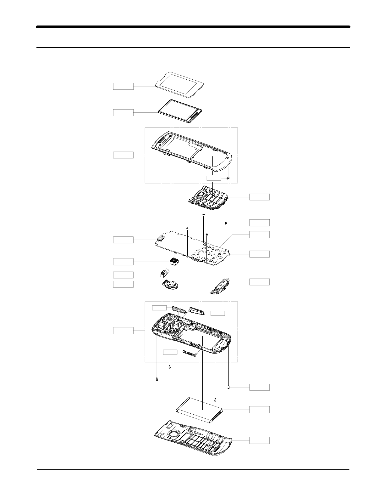
Exploded View and Parts List
4.
Cellular phone Exploded View
4-1.
QMW01
QLC01
QFR01
QMI03
QKP01
QAR01
QCA01
QMO01
QSP01
QRE01
QCR92
QME01
QMP01
QAN02
QVO01
QIF01
QSD01
QCR91
QBA01
QBC00
4-1
SAMSUNG Proprietary-Contents may change without notice
This Document can not be used without Samsung's authorization
Exploded View and Parts List
Cellular phone Parts list
4-2.
Design LOC Description SEC CODE
QSP01 SPEAKER
QAR01 AUDIO-RECEIVER
QCR91 SCREW-MACHINE
QCR92 SCREW-MACHINE
3001-002529
3009-001480
6001-002260
6001-002261
QMO01 MOTOR DC-SCH-S369 GH31-00392A
QAN02 INTENNA-GTC3200 MAIN GH42-02490A
QCA01 CAMERA MODULE-SILICON_FILE
1/5" 2M
SOCKE GH59-09289A
QBA01 INNER BATTERY PACK-AB463651BU,960MAH GH43-03216A
QME01 DOME SHEET-TF MAIN(GTC3200) GH59-09381A
QMP01 A/S ASSY-PBA MAIN(COMM) GH82-04906A
QLC01 ASSY LCD-2.0" QVGA GTC3200 GH96-04562A
QMW01 ASSY COVER-MAIN WINDOW GH98-16542A
QBC00 ASSY COVER-BATT(BLACK) GH98-17035A
QKP01 ASSY KEYPAD-(BLACK/RUSS) GH98-17318A
QRE01 ASSY CASE-REAR GH98-16540A
QSD01 PMO COVER-SD GH72-58859A
QIF01 PMO COVER-IF GH72-58861A
QVO01 PMO KEY-VOLUME GH72-58862A
QFR01 ASSY CASE-FRONT(BLACK) GH98-17038A
QMI03 RMO RUBBER-MIC HOLDER GH73-13935A
4-2
SAMSUNG Proprietary-Contents may change without notice
This Document can not be used without Samsung's authorization

MAIN Electrical Parts List
5.
Design LOC SEC CODE Description
D400
ZD303
ZD307,ZD403
ZD409
ZD306,ZD308,ZD404
ZD405,ZD406,ZD407
ZD400
ZD401
ZD301
ZD305
ZD100,ZD300,ZD408
Q300
Q305
Q303
U302
LED300,LED301,LED302
LED303,LED304,LED305
UME200
U100
PAM100
U402
U306
U401
U305
U304
U102
UCP200
TH200
R100,R101,R103,R104
R330,R337,R338,R339
R340,R341,R342,R343
R345,R346,R431
R102,R316,R318,R322
R408,R409,R410
R109,R213,R214,R215
R304,R305,R319,R329
R406
R200,R204,R209,R310
0401-001141
0403-001688
0406-001167
0406-001223
0406-001231
0406-001231
0406-001256
0406-001261
0406-001281
0406-001286
0406-001375
0501-002606
0501-002663
0502-001322
0504-001151
0601-002846
0601-002846
1108-000309
1201-002944
1201-003025
1202-001068
1203-005310
1203-005501
1203-005851
1203-006098
1205-003517
1205-004030
1404-001224
2007-000138
2007-000138
2007-000138
2007-000138
2007-000140
2007-000140
2007-000143
2007-000143
2007-000143
2007-000148
DIODE-SWITCHING
DIODE-ZENER
DIODE-TVS
DIODE-TVS
DIODE-TVS
DIODE-TVS
DIODE-TVS
DIODE-TVS
DIODE-TVS
DIODE-TVS
DIODE-TVS
TR-SMALL SIGNAL
TR-SMALL SIGNAL
TR-POWER
TR-DIGITAL
LED
LED
MEMORY
IC
IC
IC
IC
IC
IC
IC
IC
IC
THERMISTOR
R-CHIP
R-CHIP
R-CHIP
R-CHIP
R-CHIP
R-CHIP
R-CHIP
R-CHIP
R-CHIP
R-CHIP
5-1
SAMSUNG Proprietary-Contents may change without notice
This Document can not be used without Samsung's authorization

Main Electrical Parts List
Design LOC SEC CODE Description
R331,R332,R333,R334
R335
R336,R413
R201,R210,R211,R216
R434
R430
R403,R404
R312,R418,R423
R309
R303
R108,R419
R439,R440
R110
R325,R326,R327,R328
R347,R348
R107
R302
R205
R401
R315
C116,C132
C107,C324
C409,C410
C119,C421,C422
C320
C123,C212,C215
C228,C229
C131
C115,C306,C307,C400
C411,C412,C414,C429
C413
C305
C304
C121,C133,C234
C224,C236
C108,C243,C319
C118,C222
C102
2007-000148
2007-000148
2007-000157
2007-000162
2007-000166
2007-000170
2007-000172
2007-000242
2007-000831
2007-000932
2007-001119
2007-001292
2007-001307
2007-003010
2007-003010
2007-003015
2007-007001
2007-007142
2007-008736
2007-008780
2203-000254
2203-000278
2203-000311
2203-000386
2203-000425
2203-000438
2203-000627
2203-000679
2203-000812
2203-000812
2203-000854
2203-000940
2203-000995
2203-002443
2203-002487
2203-002668
2203-002709
2203-005057
R-CHIP
R-CHIP
R-CHIP
R-CHIP
R-CHIP
R-CHIP
R-CHIP
R-CHIP
R-CHIP
R-CHIP
R-CHIP
R-CHIP
R-CHIP
R-CHIP
R-CHIP
R-CHIP
R-CHIP
R-CHIP
R-CHIP
R-CHIP
C-CERAMIC,CHIP
C-CERAMIC,CHIP
C-CERAMIC,CHIP
C-CERAMIC,CHIP
C-CERAMIC,CHIP
C-CERAMIC,CHIP
C-CERAMIC,CHIP
C-CERAMIC,CHIP
C-CERAMIC,CHIP
C-CERAMIC,CHIP
C-CERAMIC,CHIP
C-CERAMIC,CHIP
C-CERAMIC,CHIP
C-CERAMIC,CHIP
C-CERAMIC,CHIP
C-CERAMIC,CHIP
C-CERAMIC,CHIP
C-CERAMIC,CHIP
5-2
SAMSUNG Proprietary-Contents may change without notice
This Document can not be used without Samsung's authorization

Design LOC SEC CODE Description
C112,C122
C128
C100
C140
C227
C129,C130,C207,C223
C425,C426
C105,C200,C203,C210
C214,C225,C230,C232
C239,C325,C416,C417
C204
C213,C218
C217,C237,C238
C220,C221
C419
C211
C209,C226,C231,C233
C240,C303,C309,C311
C321,C327,C428,C431
C432
C219,C308,C404
C408
C328,C329,C418
C117,C120,C310,C316
C317
C405
C235
C106,C323
BAT200
L121
L131
L113,L127,L128
L129
L102,L106
L107
L100,L122
L112
L115,L116
2203-005234
2203-005281
2203-005395
2203-005446
2203-005480
2203-005481
2203-005483
2203-006048
2203-006048
2203-006048
2203-006190
2203-006257
2203-006260
2203-006324
2203-006348
2203-006361
2203-006399
2203-006399
2203-006399
2203-006399
2203-006562
2203-006681
2203-006841
2203-006872
2203-006872
2203-006890
2203-007269
2203-007279
2409-001172
2703-000213
2703-001726
2703-002176
2703-002198
2703-002199
2703-002201
2703-002204
2703-002206
2703-002208
C-CERAMIC,CHIP
C-CERAMIC,CHIP
C-CERAMIC,CHIP
C-CERAMIC,CHIP
C-CERAMIC,CHIP
C-CERAMIC,CHIP
C-CERAMIC,CHIP
C-CERAMIC,CHIP
C-CERAMIC,CHIP
C-CERAMIC,CHIP
C-CERAMIC,CHIP
C-CERAMIC,CHIP
C-CERAMIC,CHIP
C-CERAMIC,CHIP
C-CERAMIC,CHIP
C-CERAMIC,CHIP
C-CERAMIC,CHIP
C-CERAMIC,CHIP
C-CERAMIC,CHIP
C-CERAMIC,CHIP
C-CERAMIC,CHIP
C-CERAMIC,CHIP
C-CERAMIC,CHIP
C-CERAMIC,CHIP
C-CERAMIC,CHIP
C-CERAMIC,CHIP
C-CERAMIC,CHIP
C-CERAMIC,CHIP
CAPACITOR
INDUCTOR-SMD
INDUCTOR-SMD
INDUCTOR-SMD
INDUCTOR-SMD
INDUCTOR-SMD
INDUCTOR-SMD
INDUCTOR-SMD
INDUCTOR-SMD
INDUCTOR-SMD
Main Electrical Parts List
5-3
SAMSUNG Proprietary-Contents may change without notice
This Document can not be used without Samsung's authorization
Main Electrical Parts List
Design LOC SEC CODE Description
L108,L109,L110,L111
L117
L130
L403
L124
L201
OSC200
OSC201
F101
F100
F102
MIC400
L404,L405
L400,L401,L402,L406
L407,L408
L200
TAC300,TAC301
RFS100
SIM300
SD300
IFC400
CN400
HEA401
BTC300
EAR400
ANT102
2703-002369
2703-002369
2703-002708
2703-003485
2703-003781
2703-003869
2801-004551
2801-004896
2904-001923
2904-001924
2909-001283
3003-001138
3301-001729
3301-001812
3301-001917
3301-002000
3404-001303
3705-001503
3709-001447
3709-001570
3710-002683
3710-003235
3711-005643
3711-007437
3722-003082
4202-001463
INDUCTOR-SMD
INDUCTOR-SMD
INDUCTOR-SMD
INDUCTOR-SMD
INDUCTOR-SMD
INDUCTOR-SMD
CRYSTAL-UNIT
CRYSTAL-UNIT
FILTER-SAW
FILTER-SAW
FILTER-DUPLEXER
MIC-CONDENSOR
CORE-FERRITE BEAD
CORE-FERRITE BEAD
CORE-FERRITE BEAD
CORE-FERRITE BEAD
SWITCH-TACT
CONNECTOR-COAXIAL
CONNECTOR-CARD EDGE
CONNECTOR-CARD EDGE
CONNECTOR-SOCKET
CONNECTOR-SOCKET
CONNECTOR-HEADER
CONNECTOR-HEADER
JACK-PHONE
ANTENNA-CHIP
SC101,SC102 GH70-03349A IPR SHIELD-CAN CLIP
Please consult the GSPN website(Samsung Portal) for the most recent version of the product's
part list.
5-4
SAMSUNG Proprietary-Contents may change without notice
This Document can not be used without Samsung's authorization
Level
6.
S/W Download
6-1.
Repair
1
6-1-1.
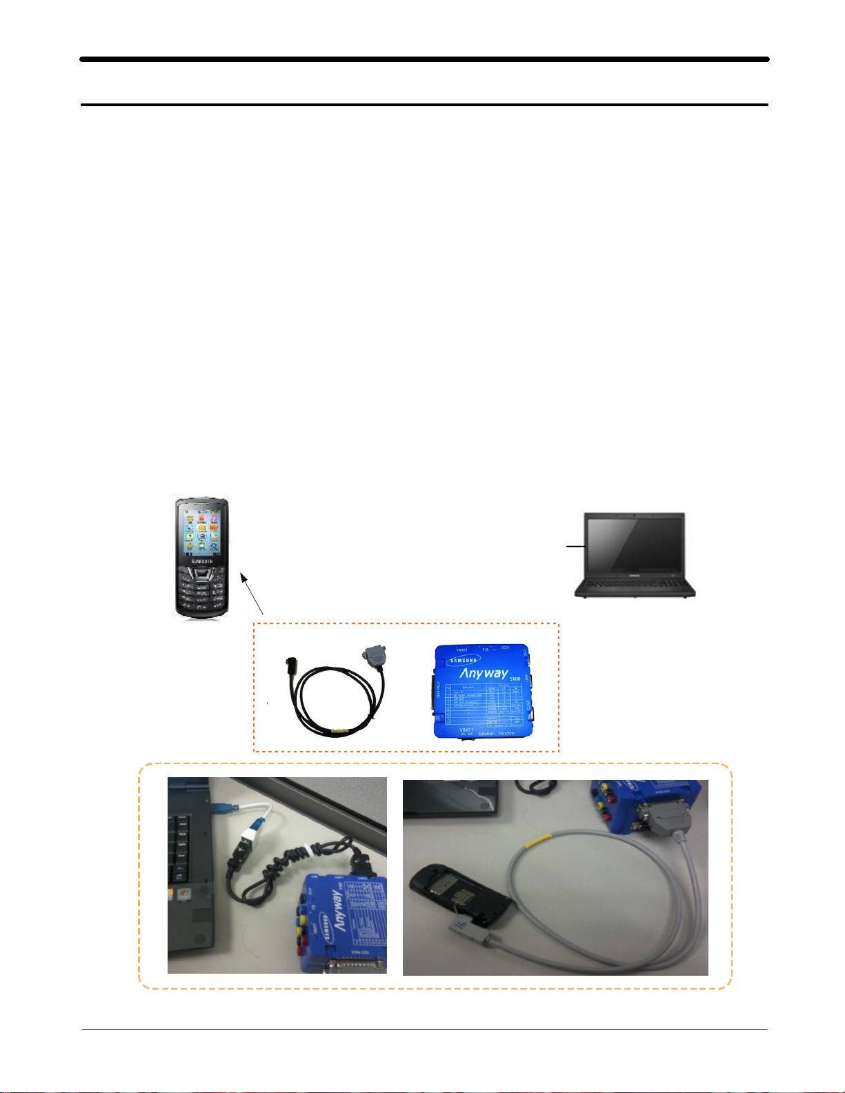
Pre-requsite for S/W Downloading
Downloader Program
•
GT-C3200 Mobile Phone
•
Data Cable
•
JIG BOX(GH99-36900A)
•
RF Test Cable(GH39-00985A)
•
JIG Cable(GH39-01160A)
•
Adapter(GH99-38251A)
•
Serial Cable
•
Binary files
•
Settings
※
Connect to ANYWAY JIG BOX
(Flash tool_E2)
JIG CABLE(Phone to JIG)
&
6-1
SAMSUNG Proprietary-Contents may change without notice
This Document can not be used without Samsung's authorization
Level1Repair
6-1-2.
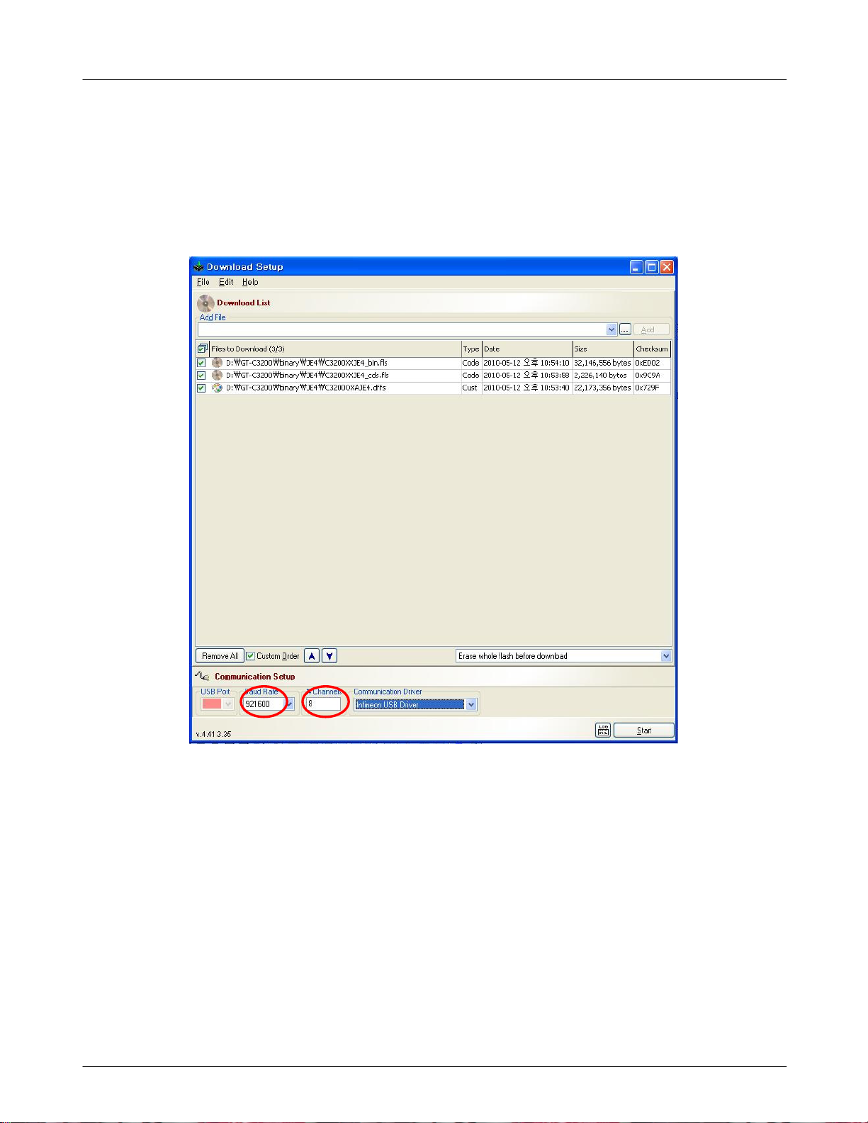
S/W Downloader Program
Load the binary download program by executing the
■
Flash tool_E2
"
Select the connected serial port and the rate of speed
.
1
"
enter this file.
←
.
6-2
SAMSUNG Proprietary-Contents may change without notice
This Document can not be used without Samsung's authorization
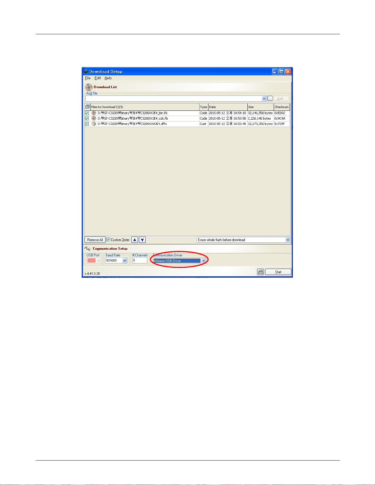
Select communication driver as Infineon USB driver.
.
2
Level1Repair
6-3
SAMSUNG Proprietary-Contents may change without notice
This Document can not be used without Samsung's authorization
Level1Repair
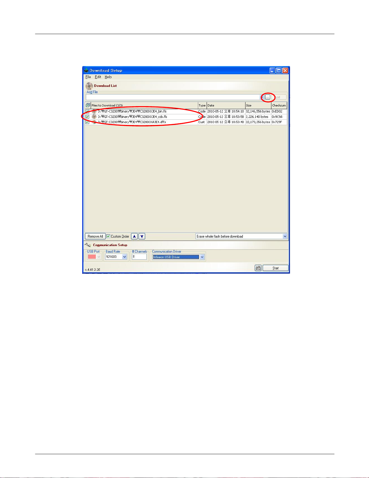
Select the Binary in sequence of_bin,_cds,.dffs.
.
3
6-4
SAMSUNG Proprietary-Contents may change without notice
This Document can not be used without Samsung's authorization
Level1Repair
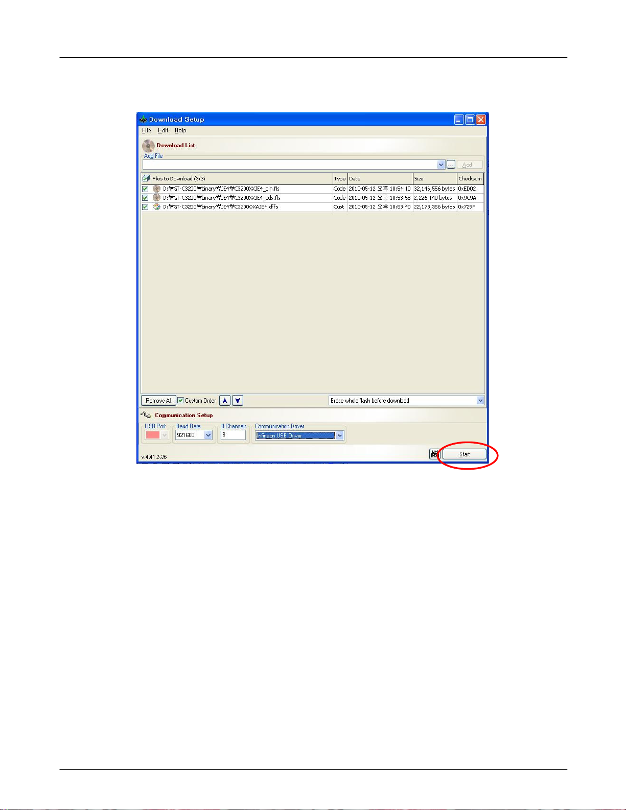
ress the"Start" button
.P
4
.
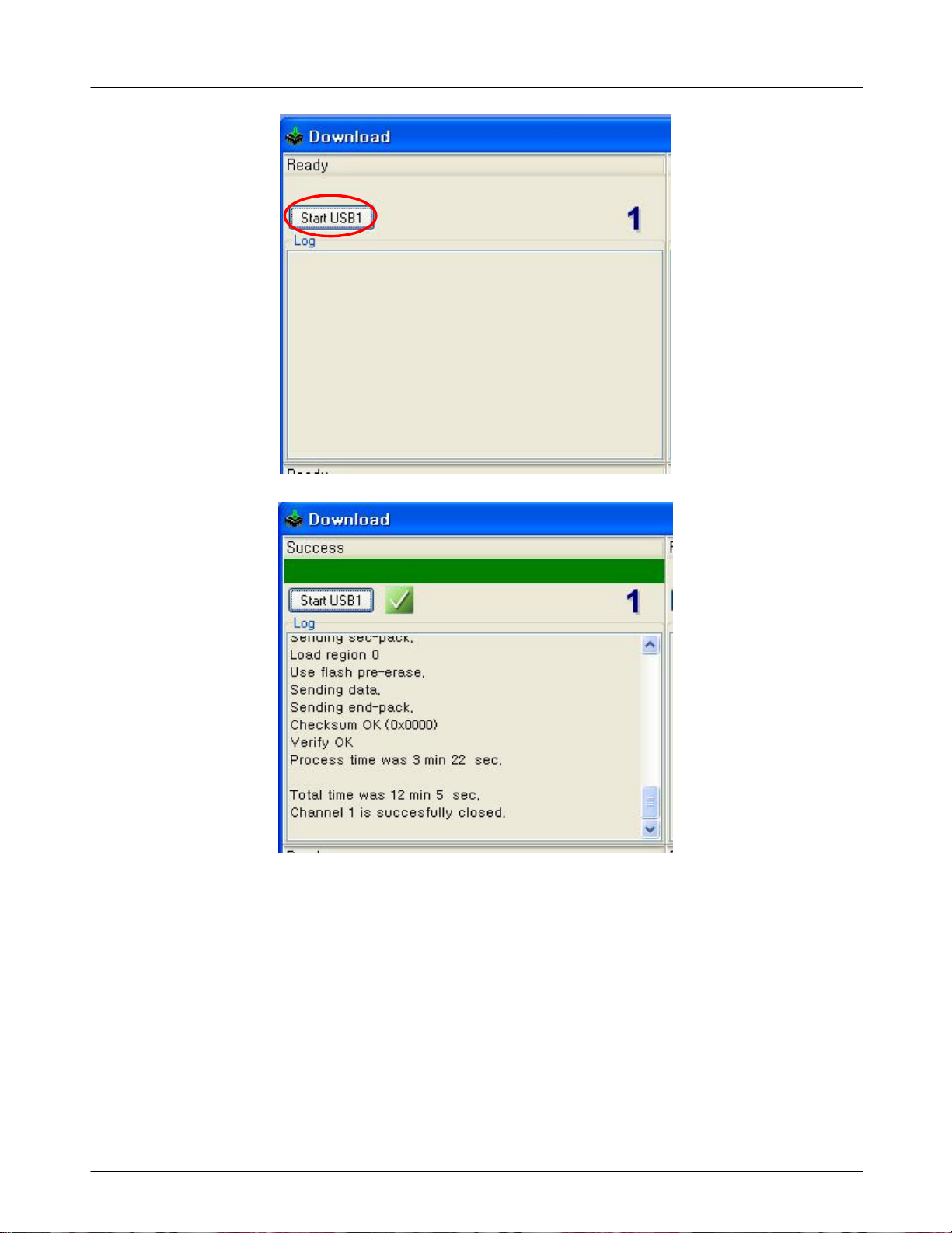
Press Start USB1 and connect the Handset.
.
5
SAMSUNG Proprietary-Contents may change without notice
This Document can not be used without Samsung's authorization
6-5
Level1Repair
When downloading is complete, you can see green bar.
.
6
Confirm the downloaded version name and etc.
7.
*#1234#
Full Reset
:
*2767*3855#
6-6
SAMSUNG Proprietary-Contents may change without notice
This Document can not be used without Samsung's authorization
:
Level
7.
Disassembly and Assembly Instructions
7-1.
Repair
2
7-1-1.
Disassembly
1
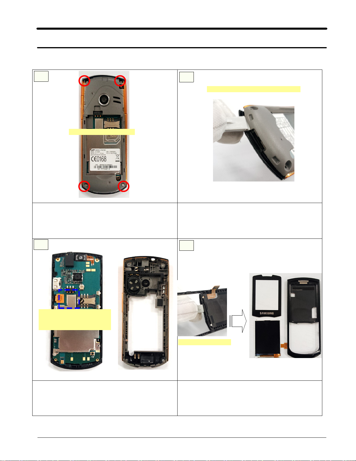
Loosen screws
1)
Loosen screws at4points.
Caution
※
Be careful not to make scratch and molding damage!
1)
2
Remove hook at the bottom
1)
Separate the rear using separation tool.
Caution
※
Be careful not to make scratch and molding damage!
1)
3
Remove LCD
connector and separate
FRONT and PBA
Remove LCD connector and separate FRONT
1)
and PBA.
Caution
※
Be careful not to make scratch and molding damage!
1)
4
Separate window
1)
Separate window and LCD.
Caution
※
Be careful not to make scratch and molding damage!
1)
7-1
SAMSUNG Proprietary-Contents may change without notice
This Document can not be used without Samsung's authorization
Level2Repair
7.
7-1-1.
Assembly
1
1)
Assemble LCD and window with FRONT.
Caution
※
Be careful not to make scratch and molding damage!
1)
2
1)
Place keypad at the FRONT.
Caution
※
Be careful not to make scratch and molding damage!
1)
3
1)
Put PBA and connect LCD.
Caution
※
Be careful not to make scratch and molding damage!
1)
4
1)
Assemble rear and joint screws at4points.
Caution
※
Be careful not to make scratch and molding damage!
1)
7-2
SAMSUNG Proprietary-Contents may change without notice
This Document can not be used without Samsung's authorization
 Loading...