

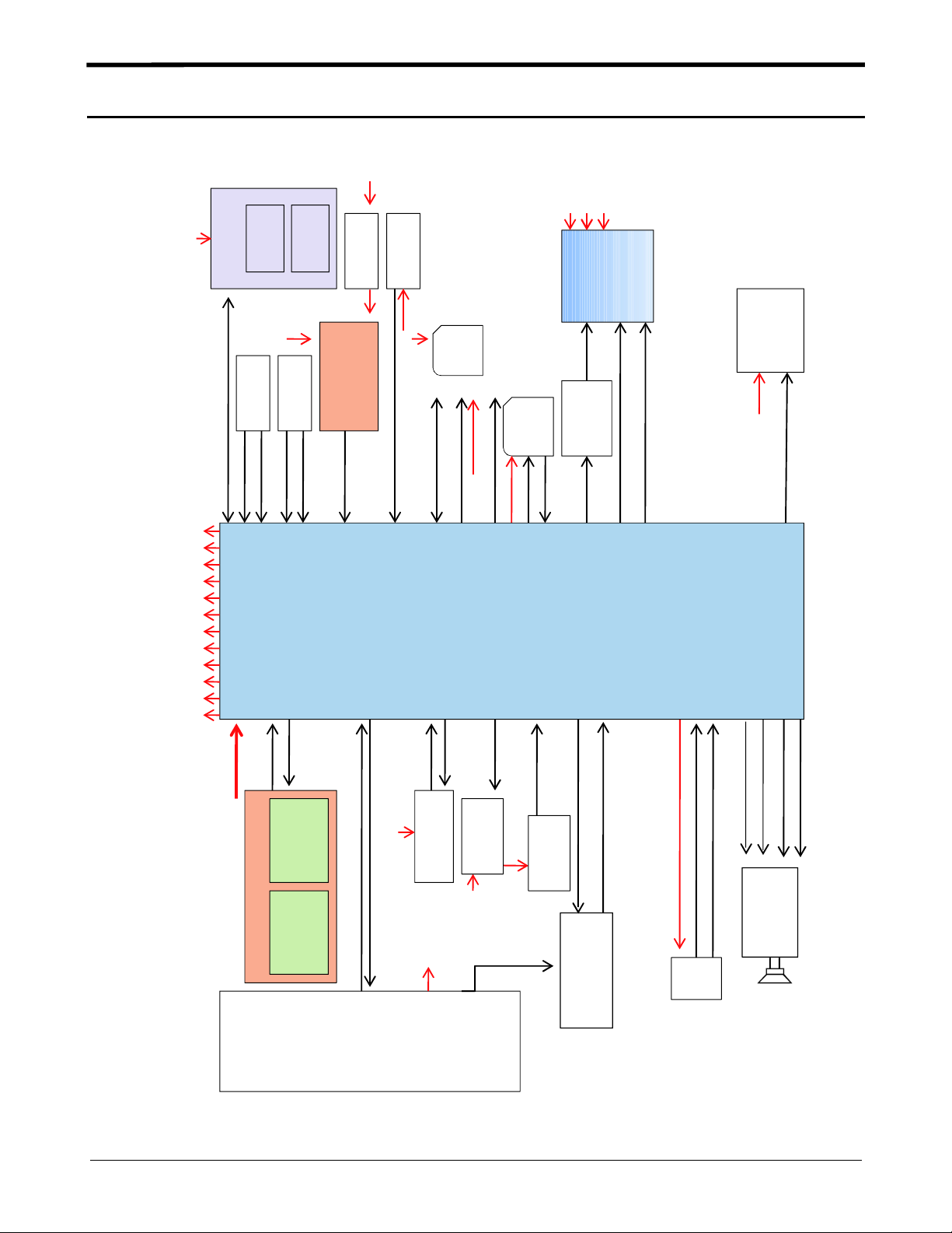
Samsung C3011 Block Diagram 7
Level
8.
Block Diagram
8-1.
V_EARMIC_2.2V
VDD_EBU_1.8V
VDD_TRX_1.4V
VDD_TDC_1.3V
VDD_RF2_2.5V
VDD_NEG_1.3V
VUSB_3. 1V
VSIM_2.85V
VMMC_2.85V
VDD_ IO_1.8V
VDD_1.8V
VDD_2.9V
Repair
3
Y
V
8
R
.
1
_
O
D
D
M
V
E
M
)
5
1
:
0
(
D
A
N
I
_
V
0
.
5
_
B
S
E
D
4
Y
0
R
M
0
O
6
0
N
5
F
8
3
F
P
z
H
L
k
A
8
T
6
-
7
.
X
2
3
N
/
N
P
/
P
X
R
X
R
M
S
S
C
G
E
D
T
A
B
V
K
C
O
L
B
F
R
b
b
M
A
M
M
8
2
R
2
1
S
1
5
P
T
A
B
V
z
O
H
X
M
C
6
T
2
2
P
X
X
S
T
T
M
B
S
A
M
/
C
R
S
1
D
,
G
S
N
E
B
E
_
X
T
2
R
0
E
0
T
Y
L
I
P
F
2
4
9
W
R
A
F
S
S
4
7
1
M
7
A
F
P
R
U
V
R
Y
O
T
8
T
1
R
P
V
O
G
N
K
I
C
G
O
R
L
A
B
H
C
G
H
C
V
,
B
S
C
,
S
C
,
J
_
1
D
X
R
,
J
_
1
J
_
D
P
X
D
T
_
,
B
D
S
X
U
R
,
_
J
1
_
T
M
R
D
A
_
U
B
,
S
U
W
,
S
J
_
_
R
V
A
5
E
_
,
S
U
N
/
B
P
V
_
,
C
I
M
M
D
_
_
X
B
S
U
A
U
C
7
E
E
T
9
N
T
T
N
R
A
B
O
C
T
U
O
_
V
5
_
S
U
B
T
V
A
B
T
V
F
V
P
D
_
B
S
D
U
X
,
T
D
_
X
M
T
_
C
1
P
T
R
A
U
,
V
2
V
.
8
.
2
_
1
_
C
I
D
D
M
V
R
A
E
_
V
,
L
/
R
_
R
A
E
M
I
A
S
B
V
H
S
-
A
V
0
.
3
_
M
I
T
S
S
O
V
I
R
_
/
K
M
I
L
S
C
_
M
I
S
T
T
K
S
B
2
_
R
3
K
_
_
L
C
C
N
_
Y
Q
S
E
_
R
M
_
C
T
P
B
N
I
_
V
0
.
5
_
S
U
B
V
M
T
K
6
L
B
2
C
K
_
L
T
C
B
4
H
0
T
O
O
T
E
U
L
B
T
A
B
V
O
A
D
0
L
1
8
M
8
A
R
S
C
C
T
A
B
V
T
N
A
_
R
A
E
_
M
F
T
L
F
A
D
S
/
L
)
C
3
V
:
8
S
0
.
(
_
1
A
S
_
T
O
D
I
A
_
S
D
D
_
D
D
D
V
S
8
0
M
8
E
8
D
B
O
M
M
P
R
W
P
_
M
A
C
_
N
E
V
V
8
8
.
.
0
1
2
7
_
_
3
M
M
5
C
A
A
I
C
C
M
V
V
V
8
.
1
_
V
2
9
.
O
2
I
_
_
T
D
D
A
B
D
D
V
V
V
D
C
L
T
F
T
”
O
.
2
)
3
:
1
(
L
B
_
D
C
L
C
I
L
B
T
C
E
T
E
D
L
_
B
D
_
S
D
C
L
_
N
E
W
L
S
C
_
S
A
/
N
A
L
D
_
)
S
7
/
M
:
T
F
0
(
S
R
D
_
_
M
M
A
A
C
C
M
A
C
D
S
E
H
7
C
L
T
7
I
0
W
7
S
B
F
G
R
B
S
C
_
L
,
S
R
_
L
,
T
S
R
_
D
C
L
,
R
W
_
L
,
D
R
_
L
,
D
)
R
7
:
_
L
0
(
,
D
M
L
L
_
L
F
T
U
O
A
N
L
_
M
F
V
2
.
2
_
C
I
M
_
V
P
N
_
_
N
N
I
I
A
A
M
M
_
_
C
C
I
I
M
M
C
I
M
R
O
T
A
R
B
I
V
T
A
B
V
N
E
_
T
O
M
P
P
_
K
P
S
N
N
_
_
_
V
V
K
C
C
P
R
R
S
W
/
S
O
I
D
U
A
K
P
S
r
o
t
c
e
n
n
o
C
F
I
8-1
Confidential and proprietary-the contents in this service guide subject to change without prior notice.
Distribution, transmission, or infringement of any content or data from this document without Samsung’swritten authorization is strictly prohibited.
Level3Repair
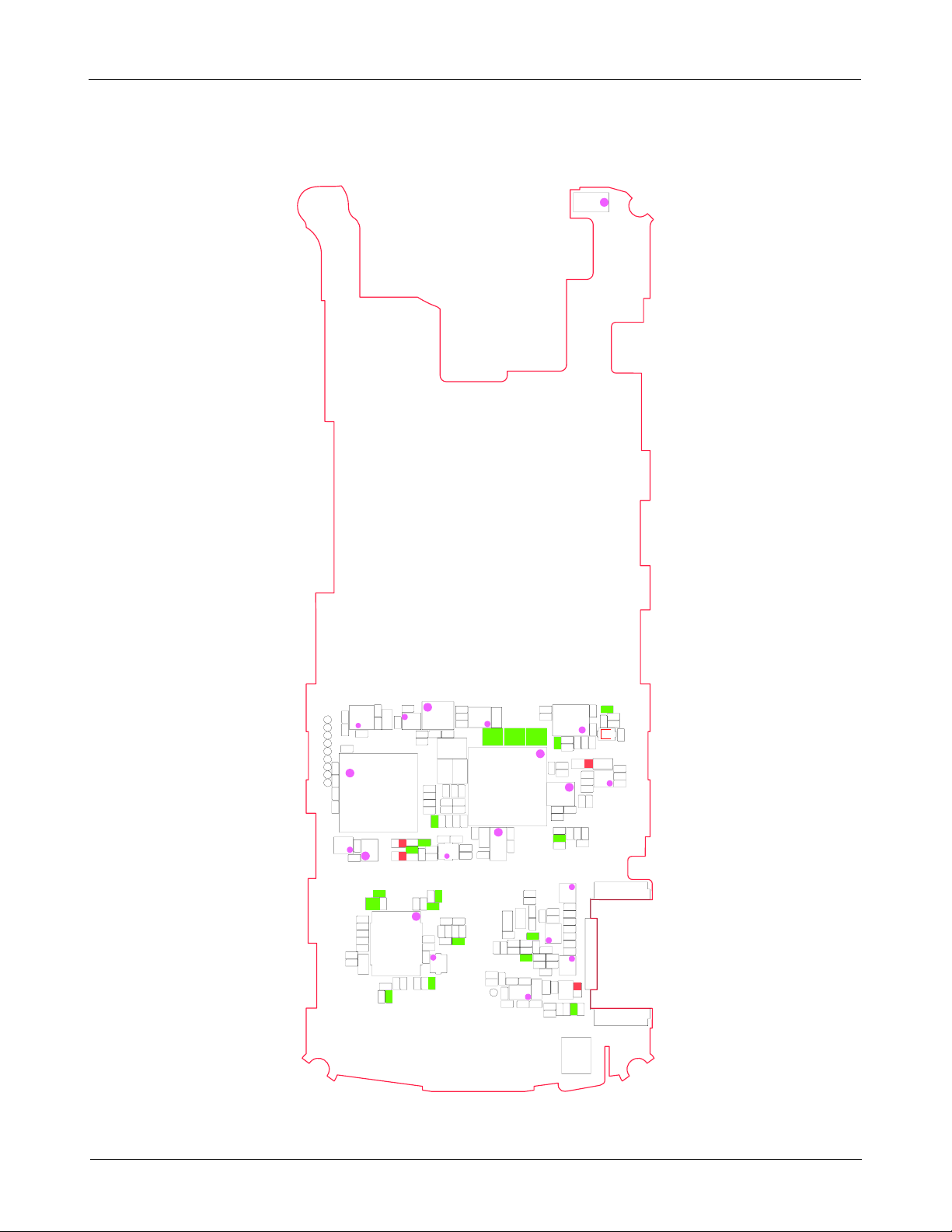
PCB Diagrams
8-2.
8-2-1.
Top
0
1
T
1
A
N
R
4
0
1
1
Q
C
6
0
0
2
4
C
TP_CS_Flash_ROM
C
TP_AD_ZERO
4
0
0
2
TP_RDn
TP_CS_RAM
6
0
2
C
TP_AD_TWO
TP_ADVn
C
2
TP_WEn
0
7
TP_WAITn
4
0
2
TP_MEM_CLK
C
5
0
2
C
R
2
0
0
0
4
0
0
3
R
3
U
R308
R104
C117
R103
4
0
C
1
C107
2
1
R
8
4
C
0
2
0
4
4
0
0
1
U
0
C
4
U200
R301
ZD302
C303
TR300
ZD301
R300
R106
C
C
1
1
9
2
1
1
5
8
1
L
P
A
2
0
1
R
1
0
1
0
1
R
0
C
1
0
3
L
1
5
0
0
2
1
2
0
1
C
C
L
1
4
0
0
3
1
L
5
0
2
R
2
0
1
2
1
2
C
R206
R208
5
1
2
C
9
2
2
C
C216
2
3
2
C
C213
C238
C203
3
3
2
C
C237
C
L
3
3
0
1
2
1
C305
4
0
3
C
1
0
3
L
C
3
R303
0
0
0
0
3
L
C
L
1
1
1
2
0
6
C
1
1
1
2
9
1
C
C122
4
4
1
C
8
0
1
L
C124
3
4
1
C
L109
0
2
1
F
C
1
0
1
C
1
0
5
2
2
1
3
1
1
L
L
C
1
2
3
0
R214
0
2
C231
U
1
2
0
L
0
1
2
C
C
C
2
2
3
3
5
4
5
1
2
R
6
1
2
R
1
4
4
1
1
2
2
2
2
C
C
C
8
0
2
O
C
9
1
S
2
R302
C
C
2
0
R309
0
0
1
3
R
C220
8
1
1
L
4
2
7
1
1
1
1
1
1
L
L
L
6
1
1
L
9
0
1
R
L200
C228
T
_
P
F
M
_
L
_
A
N
W
S
5
0
R
1
C
1
C116
0
8
6
0
1
L
U
1
0
0
C106
C411C412C413
3
0
2
R
U
P
C
2
0
0
OSC201
C202
5
2
2
C
6
2
2
C
R404
8
1
4
C
R
1
0
8
R112
0
4
5
1
C
C
4
1
1
R113
2
C
7
0
1
1
R
7
0
1
R
ZD100
C132
3
2
1
L
C133
C
0
1
3
3
1
4
2
2
1
C
L
C139
C131
7
1
R
1
5
2
1
L
C129
4
1
R
1
4
2
1
L
8
3
C
1
C
2
2
7
1
1
R
1
C135
C
C
L
1
1
2
1
4
8
2
2
6
1
0
1
U
R
1
1
6
5
1
1
R
C136C137
0
1
3
C
L303
C
1
1
5
L105
3
1
1
C
7
0
F100
1
9
0
1
C
0
0
1
R
0
1
1
C
C209
C236
1
2
2
0
2
2
C
C
1
1
2
R
0
0
2
C
R217
R209
0
2
1
C141
3
2
1
R
2
2
1
R
1
2
1
R
0
2
1
R
9
1
1
R
8
1
1
R
0
1
1
D
1
2
1
L
C
R
C
3
3
3
0
0
1
9
7
2
L
2
1
4
1
1
1
1
1
1
C
C
C
2
3
0
C
ZD300
5
0
3
R
R306
1
V300
0
7
0
3
C
3
C306
U
8
0
3
C
T
R
H
2
2
0
0
7
0
0
1
1
2
2
2
C
R
C217
U
0
0
1
C
Z
F
I
3
0
1
D
Z
C
3
1
5
Q
2
0
R
2
MIC300
8-2
Confidential and proprietary-the contents in this service guide subject to change without prior notice.
Distribution, transmission, or infringement of any content or data from this document without Samsung’swritten authorization is strictly prohibited.
Level3Repair
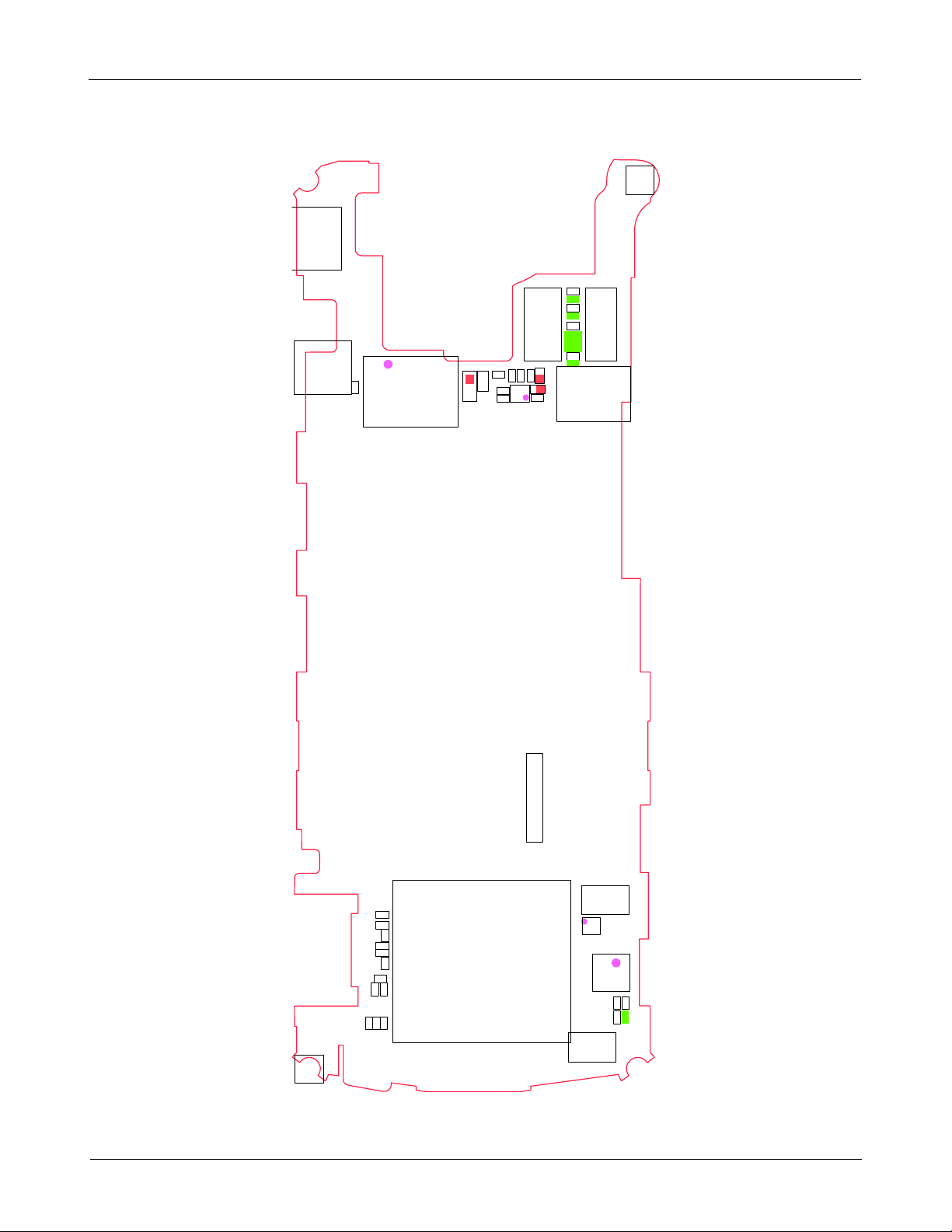
8-2-2.
Bottom
G301
0
0
3
K
P
S
C414
7
4
C
1
C415
H
1
6
4
C
D
C
4
0
1
0
0
T
O
O
R
M
3
C
3
1
3
C
3
0
1
BTC300
3
0
3
D
Z
Z
R
R
R
D
4
4
4
3
C314
0
0
0
0
2
3
0
6
ZD304
0
C405
0
4
4
0
4
C
0
3
4
C
U
0
0
4
C407
C
D
C
H
4
1
0
C408
1
0
2
R
VK300
0
0
C
N
2
3
0
0
C
D
H
C419
C422
1
1
4
R
C423
C420
0
1
4
R
C421
6
8
0
0
4
4
R
R
R
R
R
4
4
4
0
0
0
5
7
9
0
0
S
4
I
M
Z
D
3
0
5
RFS100
C
1
1
0
0
0
1
L
L
1
1
0
0
0
1
C
T
1
0
0
A
N
G300
8-3
Confidential and proprietary-the contents in this service guide subject to change without prior notice.
Distribution, transmission, or infringement of any content or data from this document without Samsung’swritten authorization is strictly prohibited.
Level3Repair
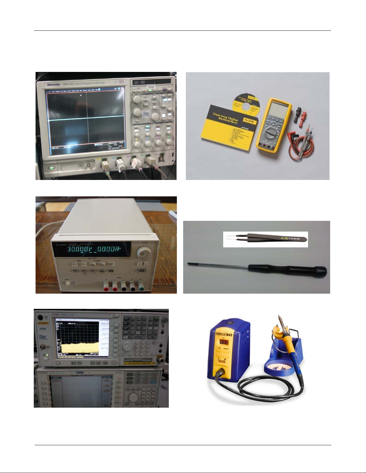
Flow Chart of Troubleshooting
8-3.
Equipments
Oscilloscope
Ç
Power Supply
á
Digital Multimeter
á
driver, ESD Safe Tweezer
á+
8960 &
Ç
Confidential and proprietary-the contents in this service guide subject to change without prior notice.
Distribution, transmission, or infringement of any content or data from this document without Samsung’swritten authorization is strictly prohibited.
Spectrum Analyzer
8-4
Soldering iron
á
8-3.
Level3Repair
LOGIC
8-1.
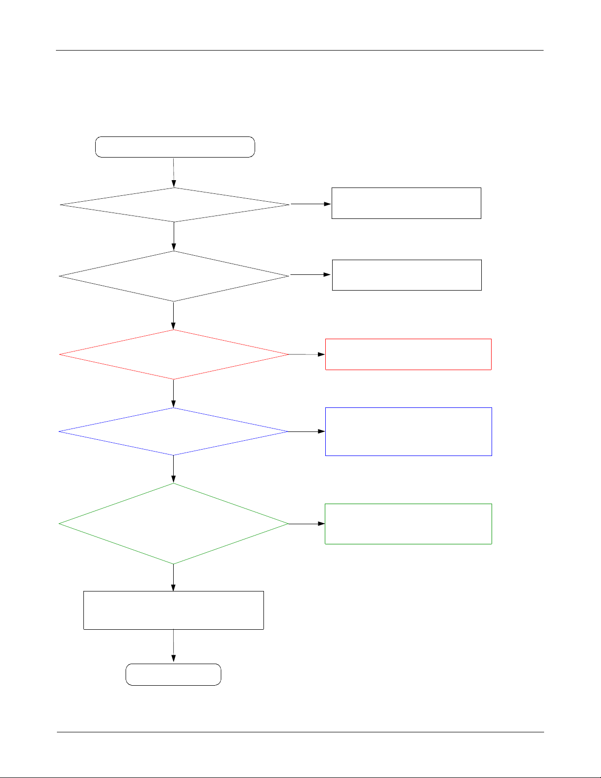
Power On
Power On'does not work
'
KEY FPCB or KEY Dome
Check the current
consumption more than
Check the Battery Voltage
is more than
Yes
damaged?
No
mA
100
Yes
3.3V
Yes
No
No
Replace Key FPCB
Download again
Change the Battery
VDD_1.8V
TP: C229)
(
Check the Clock at
UCP200 A11pin
CLK26M)
(
TP:OSC201
(
Check the initial operation
END
=1.8
Yes
=26M
1,3
Yes
Yes
HZ
pin
V?
)
No
No
Check the Main Chip related to
SD1_FB=1.8V(TP:C229)
to lookover the Chip damage)
(
Check the Main Chip
to lookover the Chip damage)
(
8-5
Confidential and proprietary-the contents in this service guide subject to change without prior notice.
Distribution, transmission, or infringement of any content or data from this document without Samsung’swritten authorization is strictly prohibited.
Level3Repair
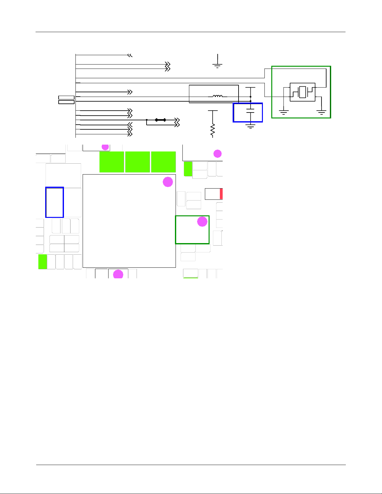
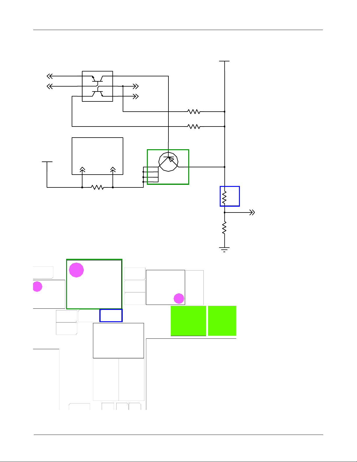
SYS
BT_REQ_CLK
3
070
3
U
_EN
F
HSL
HSR
XO
XOX
ONOFF
SD1SW
0.3T
C236(0.1T)
R208
SD1_FB
ADV_N
RD_N
RESET_N
TRST_N
WAIT_N
WR_N
R206
2
0
1
R14
T14
A11
B11
R9
R7
T6
R3
J1
L13
H15
J6
R4
K16
C231
ON_KEY
ADVn
RDn
TRSTn
WAITn
WEn
L
EAR_L
EAR_R
OSC201
NOISY
L201
VDD_IO1_1.8V
RST_BB_J
RST_BB
C411C412C413
0
0
1
R
R211
9
C
0
1
4
1
1
1
1
1
C
0
C
1
1
C
VDD_1.8V
C229
CLOSE TO THE PIN
4
3
21
C209
3
0
9
0
2
1
2
2
C
C
2
0
0
C
16
13
C238
03
2
C
C237
C
L
3
3
0
1
2
1
C
2
2
2
3
3
3
5
4
2
C
1
5
2
R
1
6
2
R
1
4
4
1
1
2
2
2
2
C
C
C
8
0
2
P
U
C
5
2
2
2
R
C236
OSC201
1
C
0
2
C202
1
1
2
R
ZD300
R
8
R
2
0
7
2
2
C
2
0
1
0
0
2
1
2
2
2
8-6
Confidential and proprietary-the contents in this service guide subject to change without prior notice.
Distribution, transmission, or infringement of any content or data from this document without Samsung’swritten authorization is strictly prohibited.
Level3Repair
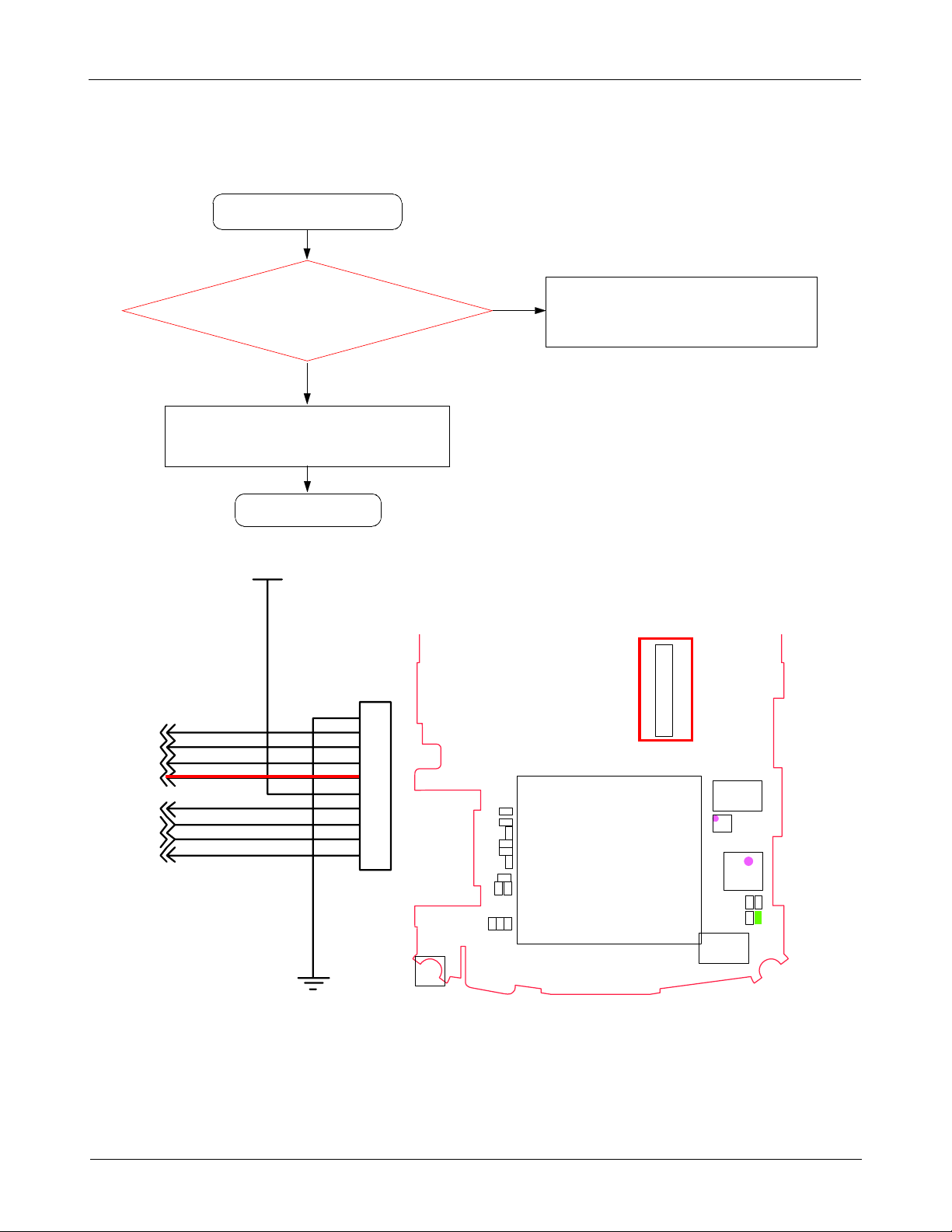
8-2.
Initial
Initial Failure
Yes
CN204(RST_BB_J
using the oscilloscope GND
SHORT PAD.
) > 1.7V?
Yes
Check the16bit data signal
memory CE
&
Yes
END
VDD_IO1_1.8V
&
No
R
Resolder UCP
ST_BB_J)must be higher than
200
1.7
V.
TMS
TDI
TCK
RST_BB_J
TRSTn
TDO
TXD1_J
RXD1_J
CN200
1
1
2
2
3
3
4
4
5
5
6
6
7
7
8
8
9
9
10
10
G300
C
N
2
0
0
0
D
0
3
C
H
C419
C422
1
1
4
R
C423
C420
0
1
4
R
C421
6
8
0
0
4
4
R
R
R
R
R
4
4
4
0
0
0
5
7
9
0
0
4
S
I
M
0
Z
D
3
0
5
0
RFS100
T
1
C
1
1
0
0
0
1
L
L
1
1
0
0
0
1
C
N
A
8-7
Confidential and proprietary-the contents in this service guide subject to change without prior notice.
Distribution, transmission, or infringement of any content or data from this document without Samsung’swritten authorization is strictly prohibited.
Level3Repair
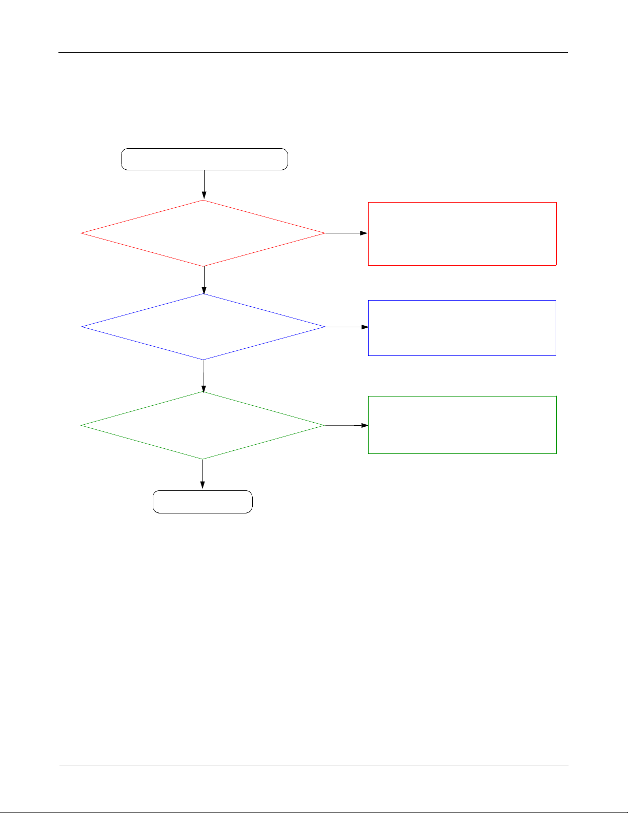
8-3.
Charging Part
Abnormal charging part
Check the Battery&TA
R206
Yes
connection.
Yes
> 4.9V?
Yes
No
No
Reinsert the Battery or TA.
Resolder R206
Check the Q201 pin
Yes
END
4 > 4.9V ?
No
Replace Q201 usingaHeatgun
8-8
Confidential and proprietary-the contents in this service guide subject to change without prior notice.
Distribution, transmission, or infringement of any content or data from this document without Samsung’swritten authorization is strictly prohibited.
CS
VBAT
Q200
1
2
34
PARALLEL FROM R310(0.075T)
N
_
E
S
N
E
S
R205
6
5
P
_
E
S
N
E
S
TNHSVBSC
VDDCHG
1
2
5
6
Level3Repair
VBUS_5V_OUT
R202
R204
3
4
Q201
R206
VCHG
R208
CHARGING CIRCUIT
0
2
2
R
Q
2
0
0
2
2
1
5
1
2
Q
2
0
1
C
C
R206R208
1
9
2
2
C
0
2
L
5
R214
C231
2
R
0
1
0
2
C
2
3
0
U
C412C413
0
1
2
C
0
8-9
Confidential and proprietary-the contents in this service guide subject to change without prior notice.
Distribution, transmission, or infringement of any content or data from this document without Samsung’swritten authorization is strictly prohibited.
0
2
P
C
U
 Loading...