

Page 1
13 Circuit Descriptions
13-1
13 Circuit Descriptions
13-1 Overall Block Structure
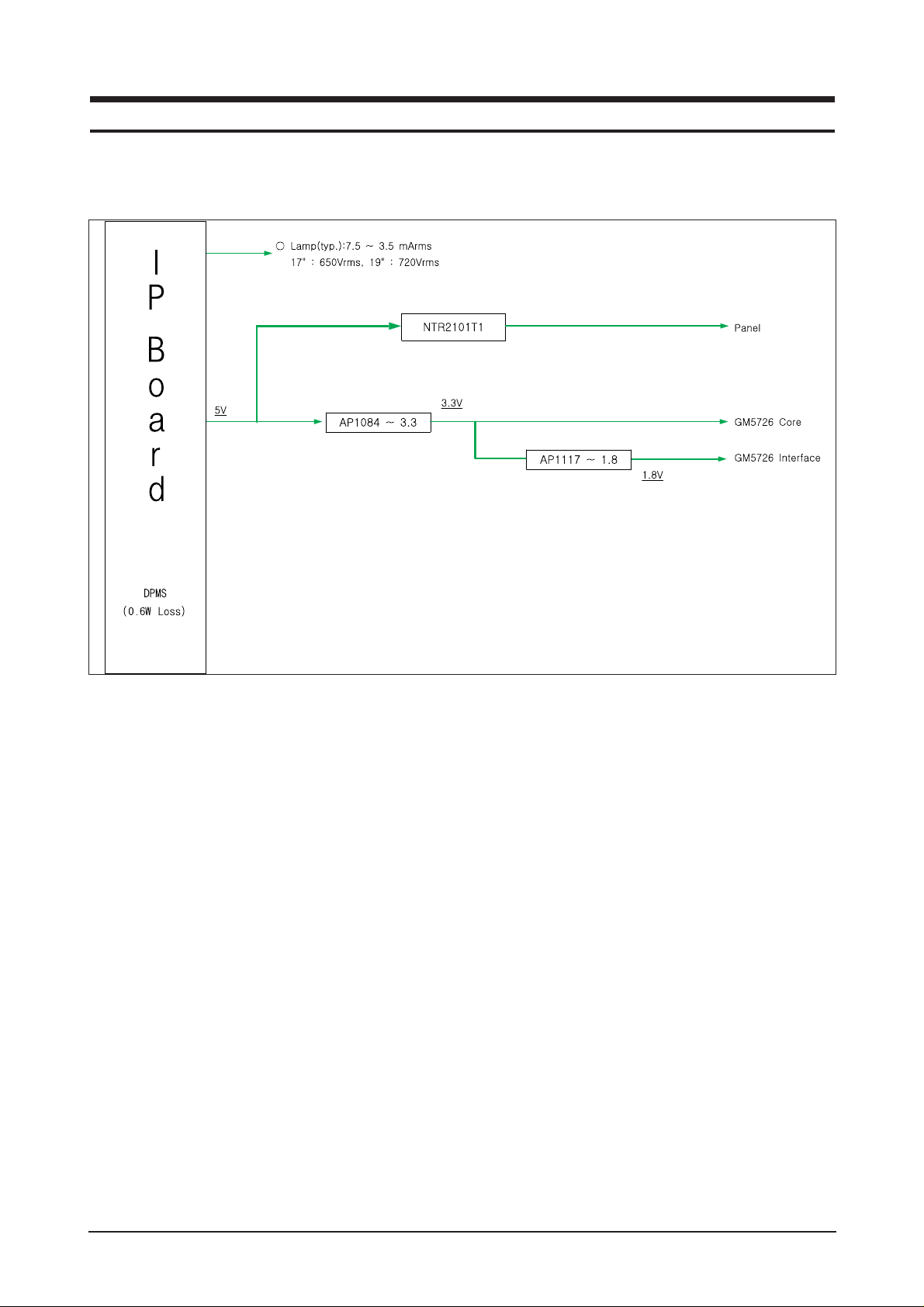
13-1-1 Power Tree
1. When the AD board is in DPMS state:
1.1 The IP has been designed so that it operates with a power consumption of less than 0.6W of.
1.2 The Scaler consumes power up to 37mA
1.3 The power to the panel is switched off
2. When the AD board is operating normally:
2.1 The maximum power consumption of the panel lamps is described below (It may vary depending on
the panel manufacturer)
17" : 4*(7.5mA*650mVrms)=4*4.9=19.6W
19: : 4*(7.5mA*720mVrms)=4*5.4=21.6W
2.2 The power consumption of the Panel Control board is as follows: 5V*720mA=3.6W
2.3 The power consumption of the Scaler is as follows: 3.3V*245mA + 1.8V*300mA = 1.35W
Page 2

13 Circuit Descriptions
13-2
13-1-2 Main Board Parts
LS17PEA, LS19PEA
LS19PEB
Page 3

13 Circuit Descriptions
13-3
1. Inverter: A conversion device that converts DC
rated voltage/current to high ones necessary
for the panel lamp.
2. DC/DC(Regulator): General term for DC to DC
converting devices.
The IP board receives 5V and outputs 1.8 or
3.3V that is supplied to the scaler (GM5726).
3. Power MosFET: The IP board receives 5V and
outputs a lower voltage in DPMS mode and
supplies the whole 5V for the panel operating
board in normal conditions. In that case, the
switching of Power MosFET is controlled by
Micom.
4. Scaler: Receives the digital TMDS and analog
R,G,B signals and convert them to proper resolutions using up- or down- scaling that are
transferred to the panel in the LDVS formats.
5. Crystal(Oscillator): Use one 14.318MHz oscillator externally to supply power to both MCU and
Scaler at the same time.
6. SCALER & EEPROM: I2C is a two-way serial
bus of two lines that supports communications
across the integrated circuits as well as
between FLASH and EEPROM.
In particular, FLASH and Scaler (GM5726) use
the SDR direct bus for mutual communications,
which is an effective, speedy system because it
allows 4 additional address/data lines compared to the old serial systems.
7. Function Key: A certain keystroke generates a
certain electrical potential, which is transferred
into ADC input port of the Scaler and then converted to a digital value by the A/D converter of
the chip. The digital value (data) is a clue to
which key is entered. In practical, the voltage
levels are set as below.
Page 4

13 Circuit Descriptions
13-4
13-1-3 IP BOARD BLOCK(POWER) Parts
13-1-4 IP BOARD BLOCK( INVERTER ) Parts
Page 5

13 Circuit Descriptions
13-5
13-1-5 IP BOARD ( inverter ) PROTECTION Parts
Figure 1.
Figure 2.
Pebble INVERTER CONTROLER FAN7310 have 2-way of the PROTECTION MODE.
1. OVP[Over Voltage Protection] : If the Voltage of the series capacitors C10 & C15 is over the 2.0V, the
Inverter latched-off.[See the Picture1]
2. OLP[Over Load Protection] : If the inverter output harness is opened(No-output current), the base of the
Q1 turns on and chage the C9 ovter 2V and then, the Inverter latchedoff[See the Picture2]
Page 6

13 Circuit Descriptions
13-6
13-2 Trouble Shooting
13-2-1 IP BOARD(Power)
Check fuse
Change FUSE
Yes
No
3 pin of FDM0565R
Vcc system in normal: HIGH
Check the Vcc system
Yes
No
1 pin of FDM0565R
Check the drain system
Normal: Switching
Check the output current
Check the main switching
Check others
Harness, Inlet
Power On
No
Check the
feedback system
No
Check the
protection system
No
Yes
Yes
Page 7

13 Circuit Descriptions
13-7
13-2-1 IP BOARD(Inverter)
Check the 13V line
Check the power system
Yes
No
1 and 2 pins of FDM0565R
Check Protection
Normal:0.6V~0.8V
Check the IC drive
Check MOSFET
Yes
No
1 and 2 pins of FDM0565R
Check Protection
Normal:0.6V~0.8V
Check the output current
Check the OVP and OLR
circuits
Check others
Power On
No
Check the feedback
system
No
Check any dimming
circuit
No
Yes
Yes
Page 8

13 Circuit Descriptions
13-8
13-3 IP BOARD(Power) Schematic Diagrams
Page 9

13 Circuit Descriptions
13-9
13-4 IP BOARD(Inverter) Schematic Diagrams
Page 10

Memo
13 Circuit Descriptions
13-10
 Loading...