

Manual
SERVICE
COLOR MONITOR
CONTENTS
1. Precautions
2. Product Specifications
3. Disassembly & Reassembly
4. Alignment & Adjustments
5. Troubleshooting
6. Exploded View & Parts List
7. Electrical Parts List
8. Block Diagram
9. Wiring Diagram
10. Schematic Diagrams
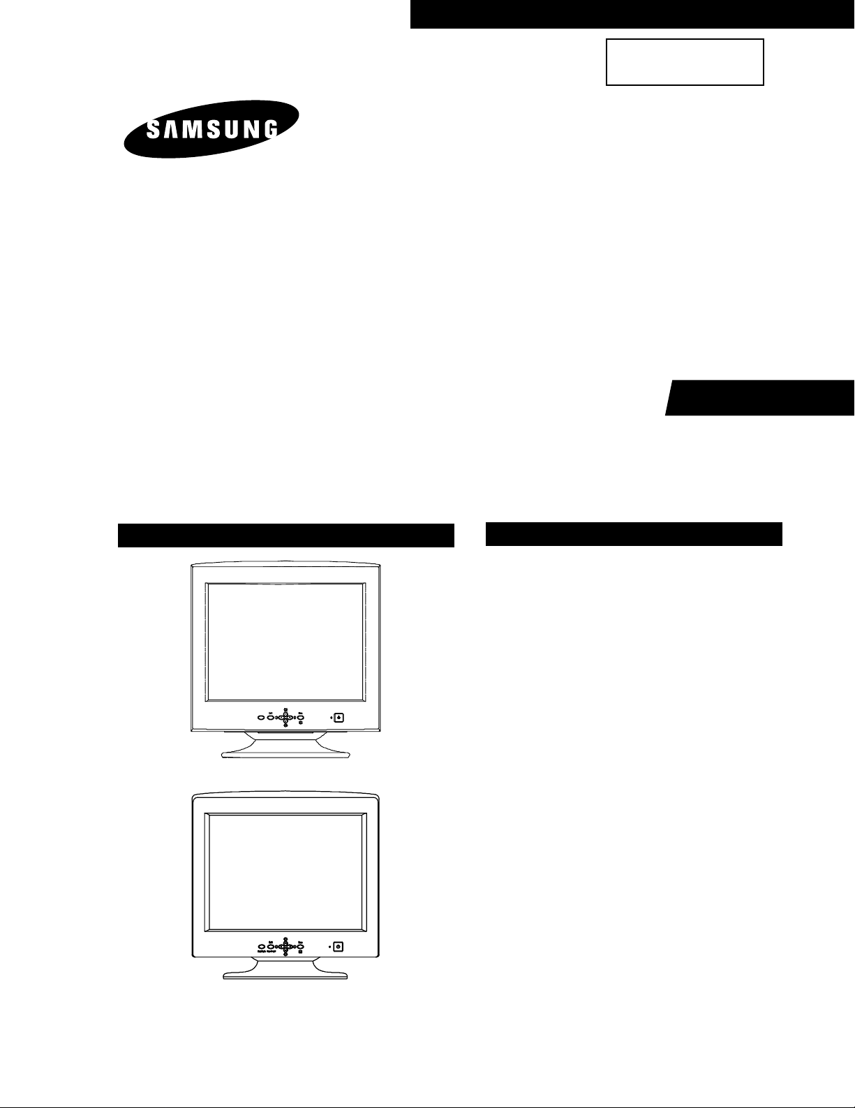
COLOR MONITOR
CA17I*(757MB)
CA19I*(957MB)
CONFIDENTIAL
CA17I*
CA19I*
Samsung Electronics Co.,Ltd.
416, Maetan-3Dong, Paldal-Gu, Suwon City, Kyungki-Do, Korea.
Printed in Korea
P/N : BH82-00002A-00
http://www.samsungmonitor.com (SyncMaster Worldwide)
http://www.samsung-monitor.com (SyncMaster USA)
http://www.sec.co.kr/monitor (Korea)
WARNINGS
1. For continued safety, do not attempt to modify the
circuit board.
2. Disconnect the AC power before servicing.
3. When the chassis is operating, semiconductor
heatsinks are potential shock hazards.
1-1-1 Servicing the High Voltage and CRT :
WARNING: A high voltage VR replaced in the wrong
direction may cause excessive X-ray
emissions.
1. When servicing the high voltage system, remove
the static charge by connecting a 10 kohm resistor
in series with an insulated wire (such as a test
probe) between the chassis and the anode lead.
2. When troubleshooting a monitor with excessively
HV, avoid being unnecessarily close to the monitor.
Do not operate the monitor for longer than is
necessary to locate the cause of excessive voltage.
3. High voltage should always be kept at the rated
value, no higher. Only when high voltage is
excessive are X-rays capable of penetrating the shell
of the CRT, including the lead in glass material.
Operation at high voltages may also cause failure of
the CRT or high voltage circuitry.
4. When the HV regulator is operating properly, there
is no possibility of an X-ray problem. Make sure the
HV does not exceed its specified value and that it is
regulating correctly.
5. The CRT is especially designed to prohibit
X-ray emissions. To ensure continued X-ray
protection, replace the CRT only with one that is
the same or equivalent type as the original.
6. Handle the CRT only when wearing shatterproof
goggles and after completely discharging the high
voltage anode.
7. Do not lift the CRT by the neck.
1-1-2 Fire and Shock Hazard :
Before returning the monitor to the user, perform the
following safety checks:
1. Inspect each lead dress to make certain that the
leads are not pinched or that hardware is not
lodged between the chassis and other metal parts in
the monitor.
2. Inspect all protective devices such as nonmetallic
control knobs, insulating materials, cabinet backs,
adjustment and compartment covers or shields,
isolation resistor-capacitor networks, mechanical
insulators, etc.
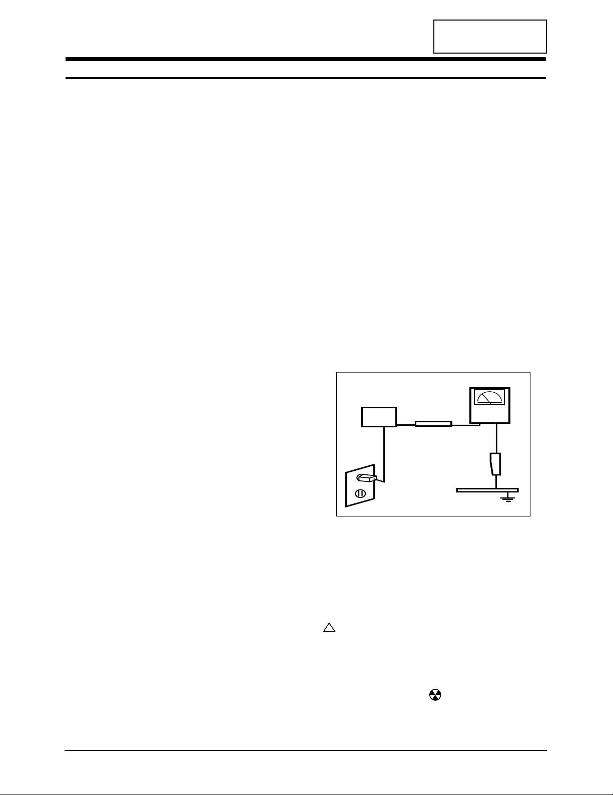
3. Leakage Current Hot Check (Figure 1-1):
WARNING: Do not use an isolation transformer during
this test.
Use a leakage current tester or a metering system
that complies with American National Standards
Institute (ANSI C101.1, Leakage Current for
Appliances), and Underwriters Laboratories (UL
Publication UL1410, 59.7).
4. With the unit completely reassembled, plug the AC
line cord directly into a 120V AC outlet. With the
unit’s AC switch first in the ON position and then
OFF, measure the current between a known earth
ground (metal water pipe, conduit, etc.) and all
exposed metal parts, including: metal cabinets,
screwheads and control shafts. The current
measured should not exceed 0.5 milliamp. Reverse
the power-plug prongs in the AC outlet and repeat
the test.
Figure 1-1. Leakage Current Test Circuit
1-1-3 Product Safety Notices
Some electrical and mechanical parts have special
safety-related characteristics which are often not
evident from visual inspection. The protection they give
may not be obtained by replacing them with
components rated for higher voltage, wattage, etc. Parts
that have special safety characteristics are identified by
on schematics and parts lists. A substitute
replacement that does not have the same safety
characteristics as the recommended replacement part
might create shock, fire and / or other hazards. Product
safety is under review continuously and new
instructions are issued whenever appropriate.
Components identified by on schematics and parts
lists must be sealed by a soldering iron after
replacement and adjustment.
1. Servicing precautions are printed on the cabinet,
CA17I*/CA19I* 1-1
1 Precautions
1-1 Safety Precautions
!
DEVICE
UNDER
TEST
TEST ALL
EXPOSED METAL
SURFACES
(READING SHOULD
NOT BE ABOVE 0.5mA)
LEAKAGE
CURRENT
TESTER
2-WIRE CORD
ALSO TEST WITH
PLUG REVERSED
(USING AC ADAPTER
PLUG AS REQUIRED)
EARTH
GROUND
CONFIDENTIAL
and should be followed closely.
2. Always unplug the unit’s AC power cord from the
AC power source before attempting to: (a) remove
or reinstall any component or assembly, (b)
disconnect PCB plugs or connectors, (c) connect all
test components in parallel with an electrolytic
capacitor.
3. Some components are raised above the printed
circuit board for safety. An insulation tube or tape
is sometimes used. The internal wiring is
sometimes clamped to prevent contact with
thermally hot components. Reinstall all such
elements to their original position.
4. After servicing, always check that the screws,
components and wiring have been correctly
reinstalled. Make sure that the area around the
serviced part has not been damaged.
1. Immediately before handling any semiconductor
components or assemblies, drain the electrostatic
charge from your body by touching a known earth
ground. Alternatively, wear a discharging wriststrap device. To avoid a shock hazard, be sure to
remove the wrist strap before applying power to
the monitor.
2. After removing an ESD-equipped assembly, place it
on a conductive surface such as aluminum foil to
prevent accumulation of an electrostatic charge.
3. Do not use freon-propelled chemicals. These can
generate electrical charges sufficient to damage
ESDs.
4. Use only a grounded-tip soldering iron to solder or
desolder ESDs.
5. Use only an anti-static solder removal device. Some
solder removal devices not classified as “anti-static”
can generate electrical charges sufficient to damage
ESDs.
5. Check the insulation between the blades of the AC
plug and accessible conductive parts (examples:
metal panels, input terminals and earphone jacks).
6. Insulation Checking Procedure: Disconnect the
power cord from the AC source and turn the power
switch ON. Connect an insulation resistance meter
(500 V) to the blades of the AC plug.
The insulation resistance between each blade of the
AC plug and accessible conductive parts (see
above) should be greater than 1 megohm.
7. Never defeat any of the +B voltage interlocks. Do
not apply AC power to the unit (or any of its
assemblies) unless all solid-state heat sinks are
correctly installed.
8. Always connect a test instrument’s ground lead to
the instrument chassis ground before connecting
the positive lead; always remove the instrument’s
ground lead last.
6. Do not remove a replacement ESD from its
protective package until you are ready to install it.
Most replacement ESDs are packaged with leads
that are electrically shorted together by conductive
foam, aluminum foil or other conductive materials.
7. Immediately before removing the protective
material from the leads of a replacement ESD,
touch the protective material to the chassis or
circuit assembly into which the device will be
installed.
Caution: Be sure no power is applied to the
chassis or circuit and observe all
other safety precautions.
8. Minimize body motions when handling
unpackaged replacement ESDs. Motions such as
brushing clothes together, or lifting your foot from
a carpeted floor can generate enough static
electricity to damage an ESD.
9. Indicates ESDs on the Schematic Diagram in
this manual.
1 Precautions
1-2 CA17I*/CA19I*
CONFIDENTIAL
1-3 Electrostatically Sensitive Devices (ESD) Precautions
Some semiconductor (solid state) devices can be easily damaged by static electricity. Such components are commonly
called Electrostatically Sensitive Devices (ESD). Examples of typical ESD devices are integrated circuits and some fieldeffect transistors. The following techniques will reduce the incidence of component damage caused by static electricity.
1-2 Servicing Precautions
WARNING1: First read the “Safety Precautions” section of this manual. If unforeseen circumstances
create conflict between the servicing precautions and safety precautions, always
follow the safety precautions.
WARNING2: A high voltage VR replaced in the wrong direction may cause excessive X-ray
emissions.
WARNING3: An electrolytic capacitor installed with the wrong polarity might explode.
CONFIDENTIAL
Picture Tube: 17-Inch (43 cm): 16-inch (40.6 cm) viewable, 19-Inch (48.2 cm): 18-inch (45.8 cm) viewable,
17”/19”: 0.26 mm Dot pitch,
Full-square tube / Perfect Flatmess, 90˚ Deflection,
Anti-Reflection coating with Anti-electrastatic, Medium short persistence phosphor
Scanning Frequency Horizontal : 30 kHz ~ 96 kHz (Automatic)
(Automatic) Vertical : 50 Hz ~ 160 Hz (Automatic)
Display Colors Unlimited colors
Maximum Resolution Horizontal : 1600 Pixels, Vertical : 1200 Pixels
Input Video Signal Analog, 0.7 Vp-p positive at 75 Ω, internally terminated
Input Sync Signal Separate Sync : TTL level positive/negative
Composite Sync : TTL level positive/negative
Sync-on-Green Coptional : Composite sync 0.3 Vp-p negative (Video on Vp-p positive)
Maximum Pixel Clock rate 250 MHz
Active Display 17” : Horizontal : 312 mm, Vertical : 234 mm / 19” : Horizontal : 352mm, Vertical : 264 mm
Input Voltage AC 90 ~ 264 Volts, 60/ 50 Hz ± 3 Hz
Power Consumption (nominal) 17”: 90 Watt , 19”: 110 Watt
Dimensions (W x D x H)
Unit / Carton CA17I* : 15.7 x 16.2 x 16.2 Inches (398 x 412 x 412 mm) / 19.3 x 22.5 x 18.0 Inches (490 x 570 x 458 mm)
CA19I* : 17.3 x 18.1 x 18.1 Inches (440 x 460 x 461 mm) / 22.1 x 25.0 x 22.1 Inches (560 x 635 x 540 mm)
Weight (Net/Gross) CA17I* : 17.0 kg (37.5 lbs) / 19.5 kg (43.0 lbs)
CA19I* : 21.0 kg (46.3 lbs) / 23.5 kg (51.8 lbs)
Environmental Considerations Operating Temperature : 32°F ~ 104°F (0°C ~ 40°C)
Humidity : 10 % ~ 80 %
Storage Temperature : -4°F ~ 113°F (-20°C ~ 45°C)
Humidity : 5 % ~ 95 %
• CA17I*/CA19I* complies with TCO 99 recommendations for reduced electromagnetic fields.
• Designs and specifications are subject to change without prior notice.
2 Product Specifications
2-1 Specifications
CA17I*/CA19I* 2-1
Item
Description
CONFIDENTIAL
2 Product Specifications
2-2 CA17I*/CA19I*
QRS
P
O
Video
Sync
Sync
Horizontal
Vertical
CDE
P
O
B
A
Video
Sync
Sync
Separate Sync
A : Line time total B : Horizontal sync width O : Frame time total P : Vertical sync width
C : Back porch D : Active time Q : Back porch R : Active time
E : Front porch S : Front porch
B
Green
Vertical
P
Q
R
S
O
Horizontal
Sync-on-Green
800/85 Hz
800 x 600
1280/85 Hz
1280 x 1024
640/85 Hz
640 x 480
VGA3/60Hz
640 x 480
VGA2/70Hz
720 x 400
Table 2-1 Timing Chart
fH (kHz)
A µsec
B µsec
C µsec
D µsec
E µsec
fV (Hz)
O msec
P msec
Q msec
R msec
S msec
Clock
Freq.
(MHz)
Polarity
H.Sync
V.Sync
Remark
31.469
31.778
3.813
1.907
25.422
0.636
70.087
14.268
0.064
1.080
12.711
0.413
28.322
Negative
Positive
Separate
31.469
31.778
3.813
1.907
25.422
0.636
59.940
16.683
0.064
1.048
15.253
0.318
25.175
Negative
Negative
Separate
43.269
23.111
1.556
3.810
5.222
17.778
85.008
13.333
0.080
0.427
12.800
0.027
36.000
Negative
Negative
Separate
53.674
18.631
1.138
2.702
14.222
0.569
85.061
11.756
0.056
0.503
11.179
0.019
56.250
Positive
Positive
Separate
91.146
10.971
0.016
1.422
8.127
0.406
85.024
11.761
0.033
0.483
11.235
0.011
157.500
Positive
Positive
Separate
1600/75 Hz
1600 x 1200
(19” Only)
106.250
9.412
0.837
1.325
6.972
0.279
85.000
11.765
0.028
0.433
11.294
0.009
229.500
Positive
Positive
Separate
Mode
IBM VESA
Timing
60.023
16.660
1.219
2.235
13.003
0.203
75.029
13.328
0.050
0.466
12.795
0.017
78.750
Positive
Positive
Separate
79.976
12.504
1.067
1.837
9.481
0.119
75.025
13.329
0.038
0.475
12.804
0.013
135.000
Positive
Positive
Separate
68.677
14.561
1.016
2.201
10.836
0.508
84.997
11.765
0.044
0.524
11.183
0.015
94.500
Positive
Positive
Separate
1024/75 Hz
1024 x 768
(17” Only)
1024/85 Hz
1024 x 768
1280/75 Hz
1280 x 1024
3-1-1 Before making Disassembly
1. Disconnect or power cord from the monitor.
2. With a pad beneath it, stand the monitor on its
front with the screen facing downward and
the base close to you.
3-1-2 Cabinet Disassembly
1. Remove the Stand from the monitor.
(Refer to Stand manual)
2. Remove 2 screws on the Rear cover.
3. Incline the monitor by lifting the rear of the
monitor.
4. Push the Opening jig each groove along the
Side of the monitor till it makes a “ttak”
sound. (2 grooves : Left and Right, Make sure
each snap is disengaged.)
5. Pull the Rear Cover up off the monitor.
CA17I*/CA19I* 3-1
CONFIDENTIAL
3 Disassembly and Reassembly
This section of the service manual describes the disassembly and reassembly procedures for the
CA17I*/CA19I* monitor.
WARNING: This monitor contains electrostatically sensitive devices. Use with caution when
handling these components.
3-1 Disassembly
Cautions: 1. Disconnect the monitor from the power source before disassembly.
2. To remove the Rear Cover, you must use the special opening jig tool.
Figure 1
Figure 2
Figure 3
Figure 4
6. Remove the Shield.(TCO 99)
7. Using pinch-nose pliers or ling-nose pliers,
acrefully disconnect the Anode Cap from the
CRT.
Warning: Do not touch the Anode contact
on the CRT (High Voltage may
remain).
3-1-3 Removing the CRT Socket PCB
1. Complete all previous steps.
2. Lift up the Video Spring and remove the CRT
Socket PCB from the CRT.
3. Disconnect all connectors on the CRT Socket
PCB.
4. Using a solder iron, disconnect 5points
Ground (GND) on the back of the Video
Shield and remove the Shield Cap.
5. Remove the screw on the front of the Shield
Socket.
6. Place the Video PCB on a flat, level surface
that is protected from static electricity.
3-1-4 Removing the Main PCB
1. Complete all previous steps.
2. Disconnect the Degaussing Coil at CN601 on
the Main PCB.
3. Disconnect all easily accessible ground wires
on the PCB and Bottom Chassis.
4. Disconnect the DY connector at the CN401
connector on the Main .
5. Using the jig, release the snaps (2) connecting
the Front Cover and the PCB then lift up the
Bottom to separate the two Shield.
6. Disconnect the Tilt connector at the CN409
connector on the Main PCB.
7. Disconnect the Sub PCB connector at the
CN204 connector on the Main PCB.
8. Remove the screws on the back and along
each side of the Bottom Chassis.
9. Carefully lift the Main PCB Ass’y and remove
the remaining ground wires.
10. Place the Main PCB Ass’y on a flat, level
surface that is protected from static electricity.
3-1-5 CRT Ass’y Disassembly
1. Complete all previous steps.
2. Straighten the Degaussing Coil Assembly
coated metal ties and lift the Coil Ass’y from
the CRT.
3. Remove the four corner screws and lift the
CRT up and away from the Front Cover
Assembly and place it on a padded surface.
Caution: Do not lift the CRT by the neck.
If you will be returning this CRT to
the monitor, be sure to place the CRT
face downward on a protective pad.
3 Disassembly and Reassembly
3-2 CA17I*/CA19I*
CONFIDENTIAL
3-2 Reassembly
Reassembly procedures are in the reverse order of Disassembly procedures.
Figure 6
Figure 7
Figure 5
4-1-1 Before Making Adjustments
4-1-1 (a) ORIENTATION
When servicing, always face the monitor to the
east.
4-1-1 (b) WARM-UP TIME
The monitor must be on for 30 minutes before
starting alignment. Warm-up time is especially
critical in color temperature and white balance
adjustments.
4-1-1 (c) SIGNAL
Analog, 0.7 Vp-p positive at 75 ohm, internal
termination
Sync: Separate/Composite
(TTL level negative/positive)
Sync-on-Green:
Composite sync 0.3 Vp-p negative
(Video 0.7 Vp-p positive)
4-1-1 (d) SCANNING FREQUENCY
Horizontal: 30 kHz to 96 kHz (Automatic)
Vertical: 50 Hz to 160 Hz (Automatic)
Unless otherwise specified, adjust at the
1024 x 768 mode (H: 68 kHz, V: 85 Hz) signals.
Refer to Table 2-1 on pages 2-2 and 2-3.
4-1-1 (e) HIGH VOLTAGE
Signal: 1024 x 768 mode (68 kHz/85 Hz)
Display image: Full white
Contrast: Maximum
Brightness: Maximum
Limit: 26 kV ± 0.5 kV (17”)
27 kV ± 0.5 kV (19”)
Measure the hight voltage level at the anode cap.
4-1-1 (f) G2 (SCREEN) VOLTAGE
The Screen Voltage is fixed in the firm so don’t
need to adjust the Screen voltage.
4-1-1 (g) CENTER RASTER
Adjust VR401 so that the back raster comes to the
center when you apply a signal of 91 kHz/85 Hz.
4-1-2 Required Equipment
The following equipment may be necessary for
adjustment procedures:
4-1-2 (a) DISPLAY CONTROL ADJUSTMENT
1. Non-metallic (–) screwdriver: 1.5 mm
Non-metallic (–) screwdriver: 3 mm
2. Philips (+) screwdriver: 1.5 mm
3. Non-metallic hexkey: 2.5 mm
4. Digital Multimeter (DMM), or
Digital Voltmeter (DVM)
5. Signal generator, or
Computer with a video board that uses the
ET-4000 chipset (strongly recommended if
using Samsung DM 200 software) and that
displays: 1280 x 1024 @ 85 Hz
6. Personal computer
4-1-2 (b) COLOR ADJUSTMENTS
1. All equipment listed in 4-1-2 (a), above
2. Color analyzer, or any luminance
measurement equipmen
4-1-3 After Making Adjustments
After finishing all adjustments, test the monitor in
all directions. If, for example, the monitor does not
meet adjustment specifications when facing north,
reposition the monitor to face east and readjust.
This time, try for an adjustment closer to the ideal
setting within the tolerance range. Test the unit
again in all directions. If the monitor again fails to
meet specifications in every direction, contact
your Regional After Service Center for possible
CRT replacement.
CA17I*/CA19I* 4-1
4 Alignment and Adjustments
This section of the service manual explains how to make permanent adjustments to the monitor.
4-1 Adjustment Conditions
Caution: Changes made without the Softjig are saved only to the user mode settings. As such, the
settings are not permanently stored and may be inadvertently deleted by the user.
CONFIDENTIAL
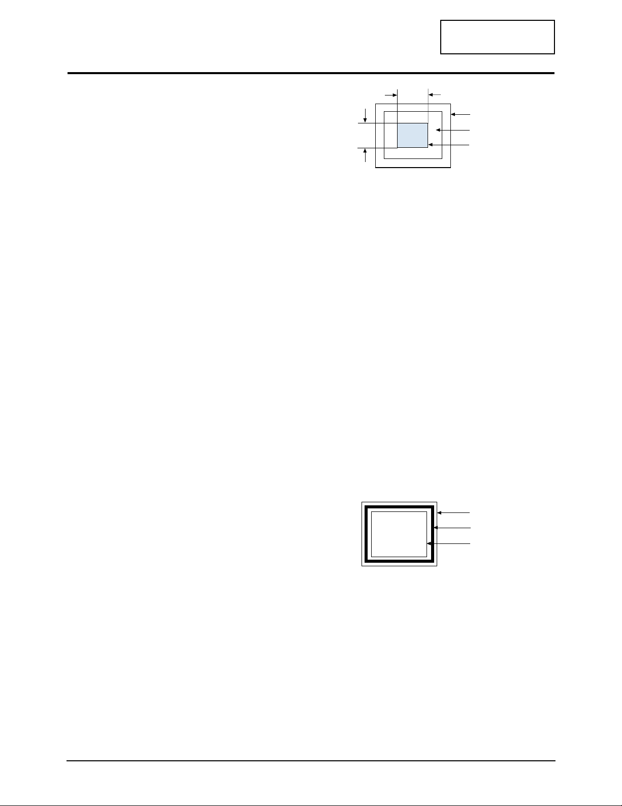
4-2-1 Centering
Centering means to position the center point of
the display in the middle of the display area.
Horizontal size and position and vertical size and
position control the centering of the display.
Adjust the horizontal size and vertical size to their
optimal settings: 312 mm (H) x 234 mm (V).
1024 x 768 mode (68 kHz/85Hz)
Adjust the horizontal position and vertical
position to ≤ 4.0 mm of the center point of the
screen.
|A-B| ≤ 4.0 mm. |C-D| ≤ 4.0 mm.
Figure 4-3. Centering
4-2-1 (a) HORIZONTAL SIZE ADJUSTMENT
CONDITIONS
Scanning frequency: 68 kHz/85 Hz
Display image: Crosshatch pattern
Brightness: Cut-off
Contrast: Maximum
Click on the << or >> box next to SIZE B+ to
adjust the horizontal size of the display pattern
to 312 mm (Tolerance: ± 3 mm) as the “H_SIZE”
is “60” on the OSD.
4-2-1 (b) VERTICAL SIZE ADJUSTMENT
CONDITIONS
Scanning frequency: 68 kHz /85 Hz
Display image: Crosshatch pattern
Brightness: Cut-off
Contrast: Maximum
Click on the << or >> box next to V_SIZE to
adjust the vertical size of the display pattern to
234 mm. (Tolerance: ± 3 mm.)
4-2-1 (c) HORIZONTAL POSITION ADJUSTMENT
CONDITIONS
Scanning frequency: 68 kHz/85 Hz
Display image: Crosshatch pattern
Brightness: Cut-off
Contrast: Maximum
Click on the << or >> box next to H_POSI to
center the horizontal image on the raster.
4-2-1 (d) VERTICAL POSITION ADJUSTMENT
CONDITIONS
Scanning frequency: 68 kHz/85 Hz
Display image: Crosshatch pattern
Brightness: Cut-off
Contrast: Maximum
Click on the << or >> box next to V_POSI to
center the vertical image on the raster.
4-2-2 Linearity
Linearity affects the symmetry of images as they
appear on the screen. Unless each row or column
of blocks in a crosshatch pattern is of equal size,
or within the tolerances shown in Table 4-1 an
image appears distorted, elongated or squashed.
Horizontal Linearity = 2x x100
Vertical Linearity = 2x x100
Table 4-1
❈ Preset Mode : 68KHz / 85Hz
Pre-load Mode : Refer to Timing Chart
4-2-2 (a) HORIZONTAL LINEARITY ADJUSTMENT
CONDITIONS
Scanning frequency: 68 kHz/85 Hz
Display image: Crosshatch pattern
Brightness: Cut-off
Contrast: Maximum
To adjust the Horizontal Linearity, refer to Table
4-1 for the tolerance range.
Click on the << or >> box next to H_LIN to
optimize the image.
Table 4-2
(Horizontal x Vertical Size Table)
4 Alignment and Adjustments
4-2 CA17I*/CA19I*
CONFIDENTIAL
4-2 Display Control Adjustments
C
A
DISPLAY AREA
EDGE OF BEZEL
B
D
Preset mode
≤ 4% ≤8%
Adjacent Linearity
Entire Linearity
Pre-load mode (48kHz~) ≤ 5% ≤ 10%
Pre-load mode (under 48kHz) ≤ 5% ≤ 14%
X max-X min
X max+X min
Y max-Y min
Y max+Y min
17” 19”
Horizantal
312 352
234 264
Vertical
4-2-2 (b) VERTICAL LINEARITY ADJUSTMENT
CONDITIONS
Scanning frequency: 68 kHz/85 Hz
Display image: Crosshatch pattern
Brightness: Cut-off
Contrast: Maximum
To adjust the Vertical Linearity, refer to Table 4-1
for the tolerance range.
Use control bar after selecting “V_LINEARITY
BAL” in left menu to optimize the image.
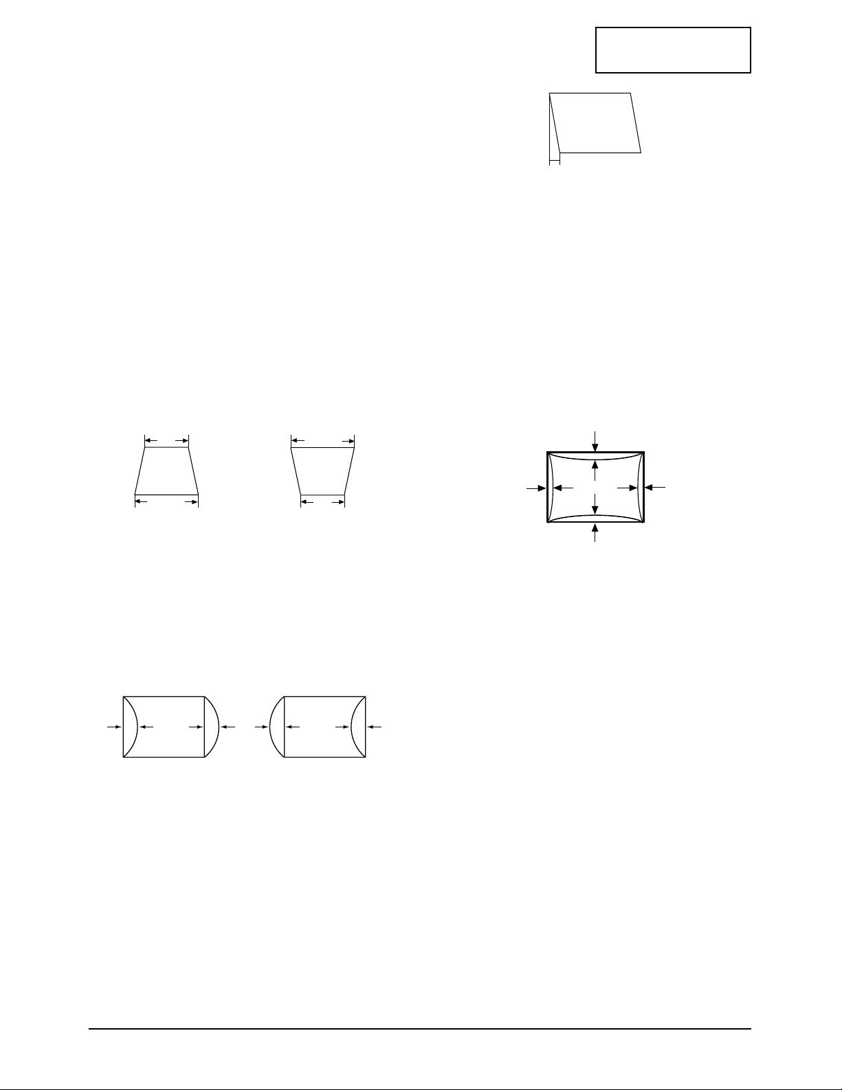
4-2-3 Trapezoid Adjustment
CONDITIONS
Scanning frequency: 68 kHz/85 Hz
Display image: Crosshatch pattern
Brightness: Cut-off
Contrast: Maximum
Use control bar after selecting “TRAPEZOID” in
left menu to make the image area rectangular.
Figure 4-4. Trapezoid
4-2-4 Pinbalance Adjustment
CONDITIONS
Scanning frequency: 68 kHz/85 Hz
Display image: Crosshatch pattern
Brightness: Cut-off
Contrast: Maximum
Use control bar after selecting “PINBALANCE” in
left menu to optimize the image.
4-2-5 Parallelogram Adjustment
CONDITIONS
Scanning Frequency: 68 kHz/85 Hz
Display image: Crosshatch pattern
Brightness: Cut-off
Contrast: Maximum
Use control bar after selecting “PARALLEL” in
left menu to make the image area rectangular.
Figure 4-6. Parallelogram
4-2-6 Side Pincushion Adjustment
CONDITIONS
Scanning frequency: 68 kHz/85 Hz
Display image: Crosshatch pattern
Brightness: Cut-off
Contrast: Maximum
Use control bar after selecting “PINCUSHION” in
left menu to straighten the sides of the image area.
4-2-7 Degauss
No adjustments are available for the degaussing
circuit. The degaussing circuit can effectively
function only once per 30 minutes.
4-2-8 Save the Data
To save the adjustment data for factory
frequencys, press FACTORY SAVE.
4-2-9 To Delete the User Mode Data
To delete the adjustment data from the user
modes, click “@4: USER DELETE” in right menu.
4 Alignment and Adjustments
CA17I*/CA19I* 4-3
CONFIDENTIAL
| C1 |, | C2 | ≤ 2.0 mm, | D1 |, | D2 | ≤ 2.0 mm.
Figure 4-7. Pincushion
A
4 mm
B
A
B
| D1 |, | D2 | ≤ 2.0 mm
Figure 4-5. Pinbalance
D1 D2 D1
C2
D2D1
C1
| A - B | < 5 mm
4-3-1 Color Coordinates (Temperature)
Color temperature is a measurement of the
radiant energy transmitted by a color. For
computer monitors, the color temperature refers
to the radiant energy transmitted by white. Color
coordinates are the X and Y coordinates on the
chromaticity diagram of wavelengths for the
visible spectrum.
CONDITIONS
Measurement instrument: Color analyzer
Scanning frequency: 68 kHz/85 Hz
Display Size : 312 (H) x 234 (V)
Display image: White flat field at
center of display area
Brightness: Cut-off
Contrast: Maximum
PROCEDURE
Use the directions in sections 4-3-2 through 4-3-4
to adjust the color coordinates for:
9300K to x = 0.283 ± 0.015, y = 0.298 ± 0.015
5000K to x = 0.346 ± 0.02, y = 0.359 ± 0.02
sRGB to x = 0.312 ± 0.02, y = 0.329 ± 0.02
4-3-2 Color Adjustments for 9300K
4-3-2 (a) BACK RASTER COLOR ADJUSTMENT
CONDITIONS
Scanning frequency: 68 kHz/85 Hz
Display image: Back raster pattern
Brightness: Cut-off
Contrast: Maximum
1. Select COLOR CHANNEL 1 to control the
color for 9300K.
2. Adjust the luminance of the back raster to
between 0.5 to 0.7ft-L using the “GREEN
CUTOFF” controls.
3. Use control bar after selecting “BLUE
CUTOFF” in left menu to set the “y”
coordinate to 0.298 ± 0.015
4. Use control bar after selecting “RED
CUTOFF” in left menu to 0.283 ± 0.015
* If color values would not be matched desirable
values, repeat sequence 3 and 4 after readjusting
“GREEN CUTOFF” control a little different.4-3-2
(b) G-GAIN ADJUSTMENT
Figure 4-8. Green Box Pattern
CONDITIONS
Scanning frequency: 68 kHz/85 Hz
Display image: Green box pattern
Brightness: Cut-off
Contrast: Maximum
1. Click on the << or >> box next to G_GAIN to
adjust the brightness of the Green Gain to
40 ± 1 ft-L.
2. Click on the << or >> box next to “BM
Contrast” to adjust the Brightness of the High
Light Gain to 88 ft-L when the High Light
function was (“BM contrast” Menu is in the
“Extra Menu”) activated.
3. Select COLOR FACTORY SAVE to save the
data.
4. Select BM OFF in right menu.
4-3-2 (c) WHITE BALANCE ADJUSTMENT
CONDITIONS
Scanning frequency: 68 kHz/85 Hz
Display image: Full white pattern
Brightness: Cut-off
Contrast: Maximum
Figure 4-9. Full White Pattern
1. Click on the << or >> boxes next to R_GAIN
and B_GAIN to make the video white.
(For 9300K color adjustment:
x = 0.283 ± 0.015, y = 0.298 ± 0.015)
Note: Do not touch the G_GAIN controls.
2. Check the ABL. If it is not within the
specifications (30 ± 1 ft-L), use the ABL
controls to adjust it.
3. Select COLOR FACTORY SAVE to save the
data.
4 Alignment and Adjustments
4-4 CA17I*/CA19I*
CONFIDENTIAL
4-3 Color Adjustments
1/3H-1/2H
1/3V-1/2V
FRONT BEZEL OPENING
BACK RASTER
GREEN WINDOW
FRONT BEZEL OPENING
BACK RASTER
WHITE WINDOW
Luminance Table (9300K) 4-3
4-3-2 (d) WHITE BALANCE ADJUSTMENT VERIFICATION
CONDITIONS
Scanning frequency: 68 kHz/85 Hz
Display image: Back raster pattern
X-Y Coordinates: x = 0.283 ± 0.02,
y = 0.298 ± 0.02
Raster Luminance 0.3 ~ 1ft-L
ABL Luminance 30 ± 1 ft-L
Brightness: Cut-off
Contrast: Maximum
1. Check whether the color coordinates of the
back raster satisfy the above spec.
If they do not, return to 4-3-2 (a) and readjust
all settings.
2. Display a full white pattern.
Note: Do not touch the G_GAIN controls.
3. Adjust the Contrast Control on the monitor so
that the luminance of the video is about 5 ft-L.
4. Check whether the white coordinates of the
video meet the above coordinates spec.
5. Adjust the Contrast Control again so that the
luminance of the video is about 20 ft-L.
6. Check whether the white coordinates of the
video satisfies the above spec.
If they do not, return to 4-3-2 (a) and readjust
all settings.
4-3-3 Color Adjustments for 5000K
4-3-3 (a) BACK RASTER COLOR ADJUSTMENT
CONDITIONS
Scanning frequency: 68 kHz/85 Hz
Display image: Back raster pattern
Brightness: Cut-off
Contrast: Maximum
1. Select COLOR CHANNEL 2 to control the
color for 5000K.
2. Adjust the luminance of the back raster to
between 0.5 to 0.7 ft-L using the G_CUT
controls.
3. Click on the << or >> boxes next to R_CUT
and B_CUT to adjust the R-Bias to x = 0.346 ±
0.02 and the B-Bias to y = 0.359 ± 0.02
4-3-3 (b) G-GAIN ADJUSTMENT
This procedure is the same as that for 9300K, refer
to the procedure on page 4-5.
You must adjust the Brightness of Green gain to
38 ± 1ft-L.
4-3-3 (c) WHITE BALANCE ADJUSTMENT
CONDITIONS
Scanning frequency: 68 kHz/85 Hz
Display image: Full white pattern
Brightness: Cut-off
Contrast: Maximum
1. Click on the << or >> boxes next to R_GAIN
and B_GAIN to make the video white.
(For 5000K color adjustment:
x = 0.346 ± 0.02, y = 0.359 ± 0.02)
2. Refer to the procedure for 9300K, section
4-3-2 (c) steps 2 and 3.
4-3-3 (d) WHITE BALANCE ADJUSTMENT VERIFICATION
Refer to the procedure for 9300K, section 4-3-2 (d).
Luminance Table (5000K) 4-4
4-3-4 Color Adjustments for sRGB
4-3-4 (a) BACK RASTER COLOR ADJUSTMENT
CONDITIONS
Scanning frequency: 68 kHz/85 Hz
Display image: Back raster pattern
Brightness: Cut-off
Contrast: Maximum
1. Select COLOR CHANNEL 3 to control the
color for sRGB.
2. Adjust the luminance of the back raster to
between 0.5 to 0.7 ft-L using the G_CUT
controls.
3. Click on the << or >> boxes next to R_CUT
and B_CUT to adjust the R-Bias to x = 0.312 ±
0.02 and the B-Bias to y = 0.329 ± 0.02.
4-3-4 (b) G-GAIN ADJUSTMENT
This procedure is the same as that for 9300K, refer
to the procedure on page 4-5.
You must adjust the Brightness of Green gain to
24 ± 1 ft-L
4-3-4 (c) WHITE BALANCE ADJUSTMENT
4 Alignment and Adjustments
CA17I*/CA19I* 4-5
CONFIDENTIAL
40 ft-L 40 ft-LWithout ABL
Without ABL
31 ft-L 30 ft-L
88 ft-L 88 ft-L
Without ABL
(High Light is Activated)
17” 19”
17” 19”
Without ABL
38 ft-L 35 ft-L
30 ft-L 30 ft-L
With ABL
CONDITIONS
Scanning frequency: 68 kHz/85 Hz
Display image: Full white pattern
Brightness: Cut-off
Contrast: Maximum
1. Click on the << or >> boxes next to R_GAIN
and B_GAIN to make the video white.
(For sRGB color adjustment:
x = 0.312 ± 0.02, y = 0.329 ± 0.02.)
2. Select COLOR FACTORY SAVE to save the
data.
Luminance Table 4-5
4-3-5 Luminance Uniformity Check
Luminance is considered uniform only if the ratio
of lowest to highest brightness areas on the screen
is not less than 7.5:10.
CONDITIONS
Scanning frequency: 68 kHz/85 Hz
(1024 x 768)
Display image: White flat field
Display size 312 (H) x 234 (V)
Brightness: Cut off point
Contrast: Maximum
PROCEDURE
Measure luminance at nine points on the display
screen (see figure below).
4-3-6 Focus Adjustment
CONDITIONS
Scanning frequency: 68 kHz/85 Hz
Display image: “H” character pattern
Brightness: Cut off point
Contrast: Maximum
PROCEDURE
1. Adjust the Focus VR on the FBT to display the
sharpest image possible.
2. Use Locktite to seal the Focus VR in position.
4-3-7 Color Purity Adjustment
Color purity is the absence of undesired color.
Conspicuous mislanding (unexpected color in a
uniform field) within the display area shall not be
visible at a distance of 50 cm from the CRT
surface.
CONDITIONS
Orientation: Monitor facing east
Scanning frequency: 68 kHz/85 Hz
Display image: White flat field
Luminance: Cut off point at the center
of the display area
Note: Color purity adjustments should only be
attempted by qualified personnel.
PROCEDURE
For trained and experienced service technicians
only.
Use the following procedure to correct minor
color purity problems:
1. Make sure the display is not affected by
external magnetic fields.
2. Very carefully break the glue seal between the
2-pole purity convergence magnets (PCM), the
band and the spacer.
3. Make sure the spacing between the PCM
assembly and the CRT stem is 29 mm ± 1 mm.
4. Display a green pattern over the entire display
area.
5. Adjust the purity magnet rings on the PCM
assembly to display a pure green pattern.
(Optimum setting: x = 0.295 ± 0.015,
y = 0.594 ± 0.015)
6. Repeat steps 4 and 5 using a red pattern and
then again, using a blue pattern.
Table 4-6. Color Purity Tolerances
(For 9300K color adjustment: x = 0.283 ± 0.02, y = 0.298 ± 0.02)
7. When you have the PCMs properly adjusted,
carefully glue them together to prevent their
movement during shipping.
4 Alignment and Adjustments
4-6 CA17I*/CA19I*
CONFIDENTIAL
Red: x = 0.620 ± 0.015 y = 0.334 ± 0.015
Green: x = 0.289 ± 0.015 y = 0.595 ± 0.015
Blue: x = 0.153 ± 0.015 y = 0.072 ± 0.015
Figure 4-10 Luminance Uniformity Check Locations
17”/19”
Without ABL
24ft-L
CONFIDENTIAL
CA17I*/CA19I* 5-1
5 Troubleshooting
5-1 Parts Level Troubleshooting
Notes: 1. If a picture does not appear, Click the Brightness and Contrast button on the front panel, and then increase the value
of Brightness and Contrast.
2. Check the following circuits.
• No raster appears: Power circuit, Horizontal output circuit, H/V control circuit, and H/V output circuit.
• High voltage develops but no raster appears: Video output circuits.
• High voltage does not develop: Horizontal output circuits.
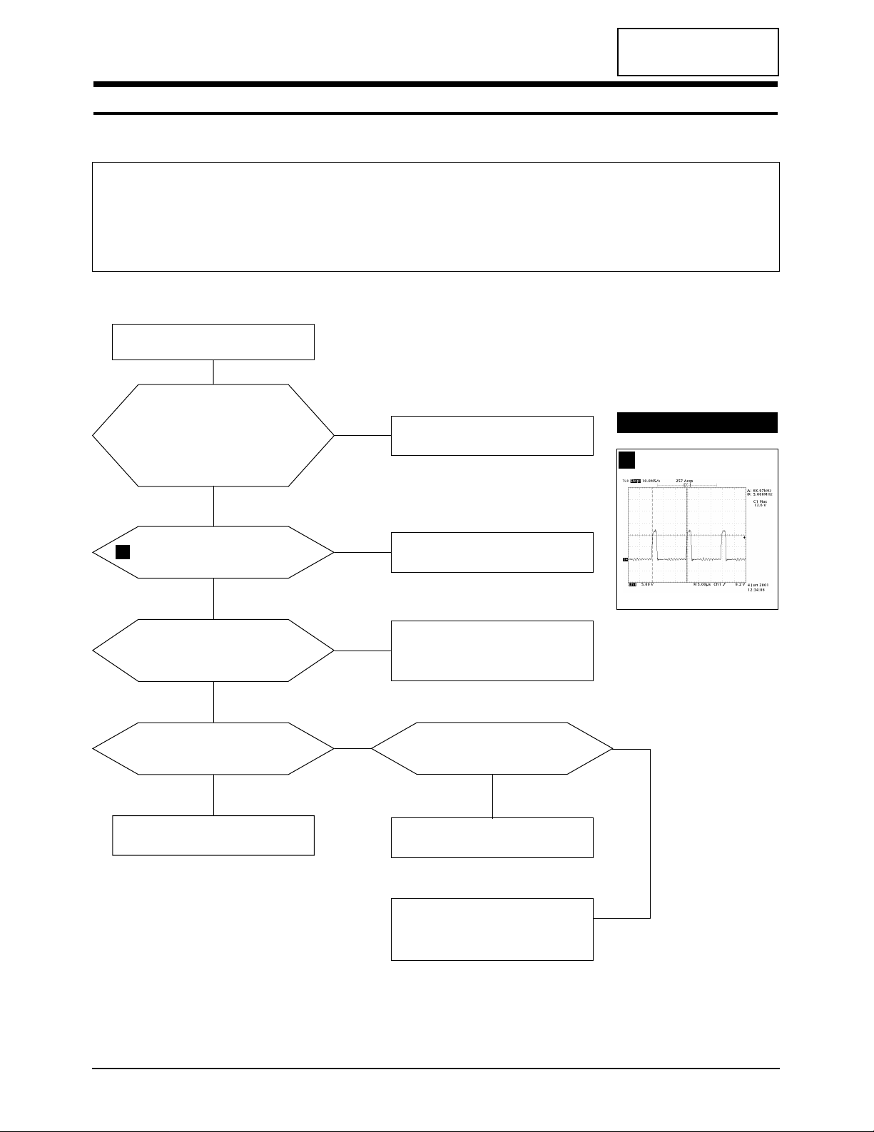
5-1-1 No Power Supply
Check and replace FG601, D601,
D701, Q701, IC601 and ZD601.
Done.
IC601 Pin 1 waveform is right?
Check and replace
IC601, ZD601, D606, IC701.
Check and Micom. (IC201)
•
Check and replace IC651.
•
Check every IC connected to 12V.
Yes
No
Check the Voltage at
C607 plus polarity point.
Is the Voltage 400VDC?
with PFC : 400VDC
without PFC : it is different
according to input voltage
Check and replace
FG601, D601, D703.
Yes
No
The secondary voltage of
T601 is right?
(Is it same the schemetic diagram)
Check TR, IC and biode
related to every B+line.
Yes
No
•
Check IC651 (KA78R12) Pin 12?
•
Is the voltage 12VDC?
Appear 4VDC Pin 4 of IC651?
Yes
No
No
Yes
1
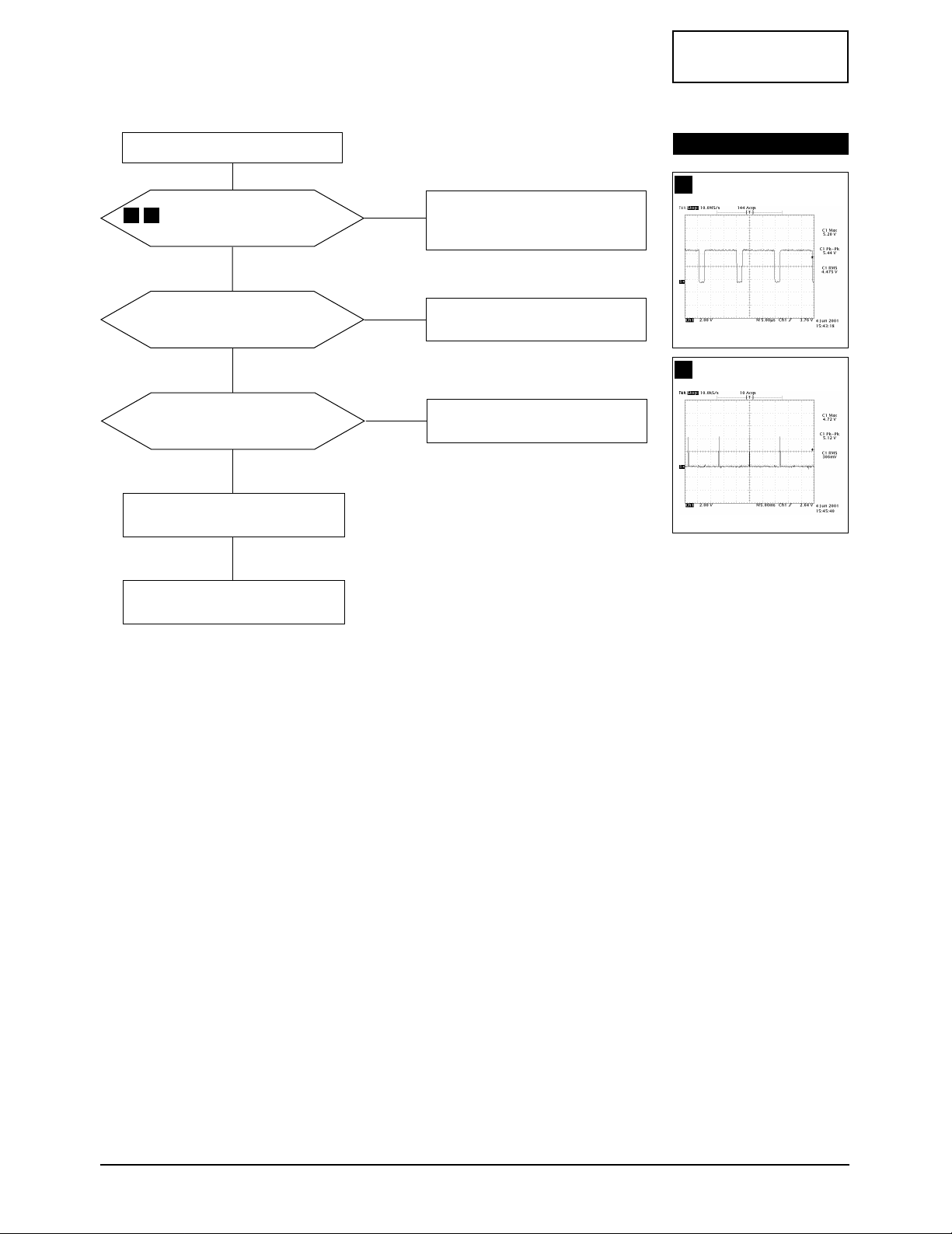
WAVEFORMS
1
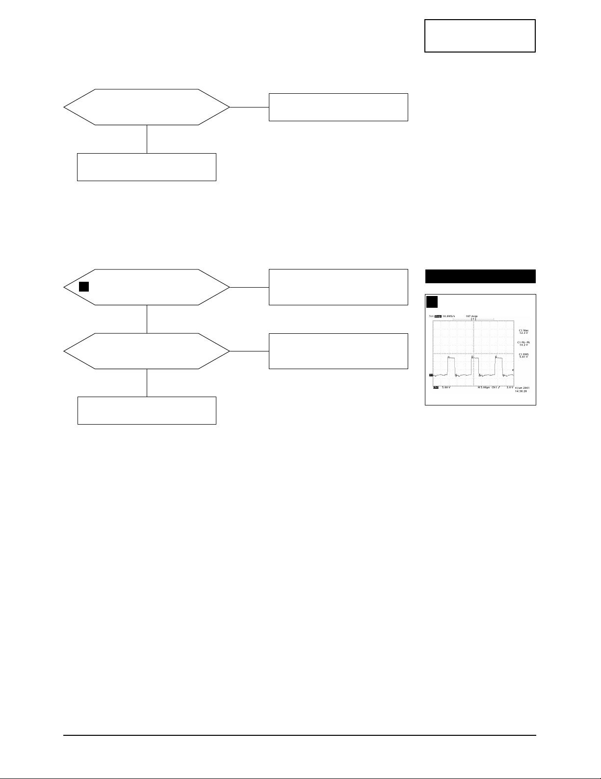
368 V (IC601, #1)
CONFIDENTIAL
5 Troubleshooting
5-2 CA17I*/CA19I*
5-1-2 PFC Failure
Check the Voltage at IC701 Pin5.
The Voltage is around 10VDC?
Check and Replace D702,
R711, ZD705, ZD706.
Yes
No
Q701 Gate waveform is right?
Replace IC701.
Yes
No
Check the Voltage at D701 cathode.
The Voltage is about 400VDC?
Replace Q701, D701.
Yes
No
Done.
5-1-3 DPMS Failure
Check signal source
H/V sync. video signal.
Make No H/V sync.
( That is power off mode).
LED blinks?
Does +12V Line off?
(Check the IC651 output Pin 2)
Check IC201 Pin 25
or replace IC201.
Yes
No
Does +14V_V Line off?
(Check the Q670 Collector)
Check Q671, D670.
Yes
No
Does the Q620 activate?
Check IC201 Pin 23
or replace IC201.
Yes
No
Done.
CONFIDENTIAL
5 Troubleshooting
CA17I*/CA19I* 5-3
5-1-4 H_Deflection Failure
IC402 Pin 6 waveform is right?
1. Appear the Voltage 12VDCat
IC402 Pin 7 replace R451.
2. Check IC402 Pins 6~5, 7~6.
3. Replace IC402.
Yes
No
Q454 drain
waveform is right?
Check Q451, Q452, Q453,
ZD450, R467, D456.
Yes
No
Q401 gate, drain
waveforms are right?
Check Q250, Q251, IC250
Check +19V line.
Yes
No
Q402 base, collector
waveforms are right?
Check and replace D402 and Q402.
Check DY connector connection.
No
2
3
4
6
5
7
WAVEFORMS
2
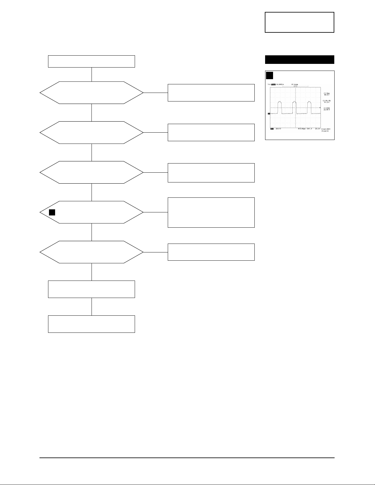
IC402, #6
CH1 P-P = 10.96 V CH1 RMS = 6.180 V
3
Q454, Drain
4
Q401, Gate
CH1 P-P = 11.6 V CH1 RMS = 6.944V
5
Q401, Drain
6
Q402, Base
7
Q402, Collector
CONFIDENTIAL
5 Troubleshooting
5-4 CA17I*/CA19I*
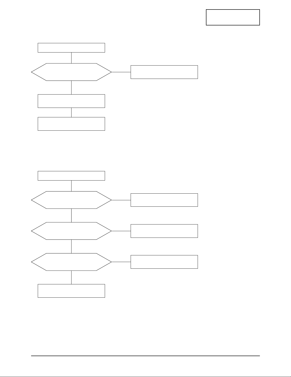
5-1-5 S Correction Failure
S1~S5 signals are right at
each frequency block?
Check S1 ~ S5 signal.
Refer to the S-corrction table page?
Check and replace
C411, C413, C414, C415, C416,
C417, C418, Q403 ~ Q407, Q408 ~ Q412
Yes
5-1-6 H_Lin. Failure
IC201 Pin 3 voltage varies with
different H_Lin. DAC values?
IC403 Pin 7, 8 voltage varies with
different H_Lin. DAC values?
Check +12 V line.
Check some parts around IC403.
Check L403.
Yes
Yes
No
IC402 Pin 6 output duty varies with
different H_Size DAC values?
Check some parts
around IC250, IC201.
Yes
No
Check and replace IC201.
No
Replace IC201.
No
5-1-7 Invariable H_Size
D250 Cothode voltage varies with
different H_Size DAC values?
Check and replace IC250, IC201.
No
CONFIDENTIAL
5 Troubleshooting
CA17I*/CA19I* 5-5
5-1-8 Abnormal H_Size
The Voltage waveforms at
Q402 Collector are right?
Repeat the troubleshooting
Guide of H_deflection failure.
Check some parts around
IC250 and IC402 Pin 1 and 2.
Yes
No
5-1-9 Side Pin or Trap Failure
IC250 Pin 24 output exists?
The waveform is right?
Check and replace IC250.
5-1-10 Para. or Pin Balance Failure
IC250 Pin 24 output varies with
different DAC values?
No
Replace IC261.
No
7
T402 pin 8 wareform is right?
Replace T402.
Yes
Check and replace IC402.
Check some parts IC402 Pin 2
and IC250 Pin 24.
Yes
No
8
9
WAVEFORMS
8
T402, #8
WAVEFORMS
9
IC250, #24
7
Q402, Collector
CONFIDENTIAL
5 Troubleshooting
5-6 CA17I*/CA19I*
5-1-11 Tilt Failure
IC201 Pin 5 output duty varies
with different DAC values?
IC403 Pin 10, 11 output varies with
different DAC values?
Check and replace IC403.
Check and replace CRT.
Yes
Yes
No
Check and replace IC201.
No
Check tilt connector connection
5-1-12 V Deflection Failure
Is 14V at IC301 Pin 2?
Is -14V at IS301 Pin 5?
IC250 Pin 23 output exists?
The waveform is right?
Check and replace IC250.
Yes
Yes
No
Check and replace R312, R316.
Refer to 5-1-1 No Power supply.
No
IC301 Pin 6 output exists?
The waveform is right?
Check and replace some
parts around IC301.
Yes
No
Check V DY connector connection.
10
11
WAVEFORMS
10
IC250, #23
11
IC301, #6
CONFIDENTIAL
5 Troubleshooting
CA17I*/CA19I* 5-7
5-1-13 V Size or Pos. Variation Failure
IC250 Pin 23 output varies with
different DAC values?
Yes
Check some parts around IC250.
Check bias voltage.
Check and replace IC250 and IC301.
No
5-1-14 High Voltage Failure
Q504 gate driving pulse exist?
The waveform is right?
Check +12 V line.
Check and replace
Q502, Q503, R511, IC501.
Yes
No
Done.
12
Are there some voltages
(350V, 30V, -210V, etc)
at secondary part of FBT?
Check and replace Q504, D508,
D509, D530, D507, D505.
Yes
No
WAVEFORMS
12
Q504, Gate
CONFIDENTIAL
5 Troubleshooting
5-8 CA17I*/CA19I*
IC102 Pin12 input exists and
varies with different patterns?
Check and replace IC102
(19”:IC101)
.
Input full white pattern to monitor.
No
Yes
T501 Pin 8 Voltage exists?
Check and replace T501.
Yes
No
IC103 Pin 16 output exists and
varies with different patterns?
Check and replace IC103.
Yes
No
Check and replace IC102 and CRT
Check CN102, Q101, Q102, ZD101.
5-1-15 ABL Failure
5-1-16 Focus Failure
IC250 Pin 11 and 32
output are right?
Check and replace IC261.
Yes
No
Some parts around Q551,
Q552, Q553 and Q540 are right?
Replace failed part.
Yes
No
Some parts around T502 are right?
Replace failed part.
Check the connection between FBT
Pin 13, CRT Socket PCB.
Yes
No
13
14
Does the voltage of Q541
collector change as the FH function
is changed on the OSD menu?
Check Q541 and others components.
Yes
No
WAVEFORMS
13
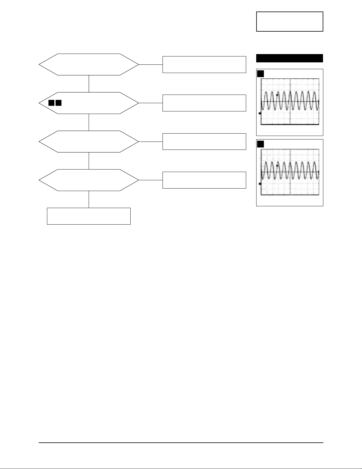
2.20 V (IC250, #11, 32)
CH1 P-P = 2.20 V CH1 RMS = 2.776 V
14
580 V (T502, #1)
CH1 P-P = 580 V CH1 RMS = 278.2 V
CONFIDENTIAL
5 Troubleshooting
CA17I*/CA19I* 5-9
5-1-17 No Video
IC101 Pins 2, 4 and 6
inputs are right?
IC101 Pins 20, 22 and 24
outputs are right?
Check Vcc on IC101
and replace IC101.
Yes
Yes
No
Check CN101, IC1, QR51, QG51,
QB51, and IC3 on BNC Board.
No
IC102 Pins 25, 28 and 30
outputs are right?
Check +12 V line.
Check and replace IC102.
Yes
No
Are there waveforms at CRT
Socket Pin Red, Green, Blue?
Check +80 V line.
Check and replace IC105 and
components around IC105.
Yes
No
G2 voltage is right?
Heater Voltage is right?
Check D598, D599 and G2 wire.
Check CN102 wire Assy.
Change CRT.
Yes
Done.
No
Check signal cable and connection.
15
WAVEFORMS
15
CRT Socket, Red, Green, Blue
CONFIDENTIAL
5 Troubleshooting
5-10 CA17I*/CA19I*
5-1-18 Micom Failure
IC201 Pin 13 input is over 4.2V?
IC201 Pin 32 and 33
inputs are right?
Check X201, C203 and C204.
Yes
Yes
No
Check IC650.
No
IC201 Pin 40 input is High Active?
Check and replace IC202.
Yes
No
All in/output values are right?
Replace IC201.
Yes
No
Done.
16 17
WAVEFORMS
16
3.42 V (IC201, #33)
CH1 P-P = 3.42 V CH1 RMS = 2.500V
17
3.16 V (IC201, #32)
CH1 P-P = 3.16 V CH1 RMS = 2.560 V
CONFIDENTIAL
5 Troubleshooting
CA17I*/CA19I* 5-11
5-1-19 OSD Failure
IC103 Pin 6 and 17
waveforms are right?
Is there 5V on IC103 Pin 5 and 24?
IC102 Pins 1, 2 and 3, 4 (19”: IC101
Pins 1, 4 and 9, 13) input is right?
Check and replace IC103.
Yes
Yes
No
Check and replace
Q104, IC201 Pin 20.
Check 5V Line.
No
Does the Voltage Change on
IC201 Pins 11, 12 When you
push the control Button?
Check CN204 and Assy.
Yes
No
Check IC201.
Done.
Check CN102 and connector Ass’y.
18 19
WAVEFORMS
18
IC103, #6, 17
19
IC103, #5, 24
CONFIDENTIAL
5 Troubleshooting
5-12 CA17I*/CA19I*
RL601 operation is right?
Q601 base input is right?
Check and replace Q601.
No
Yes
No
Yes
Check D-Coil, POS601.
Yes
IC201 Pin 31 output is right?
Check and replace IC201.
Check user function key.
No
Done.
Check degaussing connector.
5-1-21 Degaussing Failure
5-1-20 User Control Failure
IC201 Pins 11 and 12 inputs are
right at each function?
Check and replace function key.
Check and replace IC201.
Done.
Yes
No
Check connector Ass’y.
 Loading...