

Samsung 757DFX Service manual
SyncMaster
757 DFX
Parametry SyncMaster 757DFX
17”
Obrazovka: Velikost 17” (16” viditelná)
Technologie masky - ultraplochá obrazovka
Rozteč bodu 0,20 mm (H)
Povrch Několikanásobná antireflexní vrstva
Vstupní signál: Video signál analogový RGB
Sync signál Oddělený H/V, kompozitní
Horizontální frekvence 30 - 96 kHz
Vertikální frekvence 50 - 160 Hz
Max. šířka pásma 250 MHz
Rozlišení: Maximální 1920 x 1440 / 64 Hz
VESA 1800 x 1440 / 64 Hz
1856 x 1392 / 66 Hz
1792 x 1344 / 68 Hz
1600 x 1200 / 68 Hz
1280 x 1024 / 79 Hz
1152 x 864 / 93 Hz
1024 x 768 / 104 Hz
800 x 600 / 131 Hz
640 x 480 / 160 Hz
Doporučené 1024 x 768 / 85 Hz
1280 x 1024 / 85 Hz
Velikost zobrazení: Normální 312 x 234 mm
Maximum 325 x 244 mm
Vstup signálu: Konektor 15 pin
Příkon Při práci maximálně 90 Wattů
Vypnutý ≤ 3 Watt
Příkon: Norma EPA / Energy 2000 / VESA DPMS
Vlastnosti: DDC DDC 2B / 2Bi / GTF
HIGHLIGHT ZONE
™
ano
USB (upstream + kabel) ano
Uživatelské nastavení: Display Director™ jas, kontrast, pozice, velikost, zoom, poduška,
trapézovitost, paralelogram, balance hrotu,
V - linearita, teplota barev, Degauss, úroveň
vstupního signálu, tovární reset, časování
obrazu, H/V-Moire, jazyk, OSD zámek,
horní a dolní rohy, synchronizace typu vstupu,
HIGHLIGHT ZONE
™
, rotace
OSD: ano
Bezpečnost & EMC: Bezpečnost UL, CSA, TuV, CB, NEMKO, Korea EK, CCIB,
PSB, NOM, GOST, CDRH, IRAM
EMC FCC, CE, VCCI, C-tick, BSMI, Mic, ICES
Nízké vyzařování TuV GS, MPR II, TCO99 (volitelné)
Rozměry: Produkt (š x h x v) 398 x 412 x 412 mm
Hmotnost: Netto 17 kg
Brutto 19,5 kg
Příslušenství: Software instalační ovladače, manuál,
Natural Color
™
, MouScreen
™
Multimediální stojan na přání
HBC-Focus
™
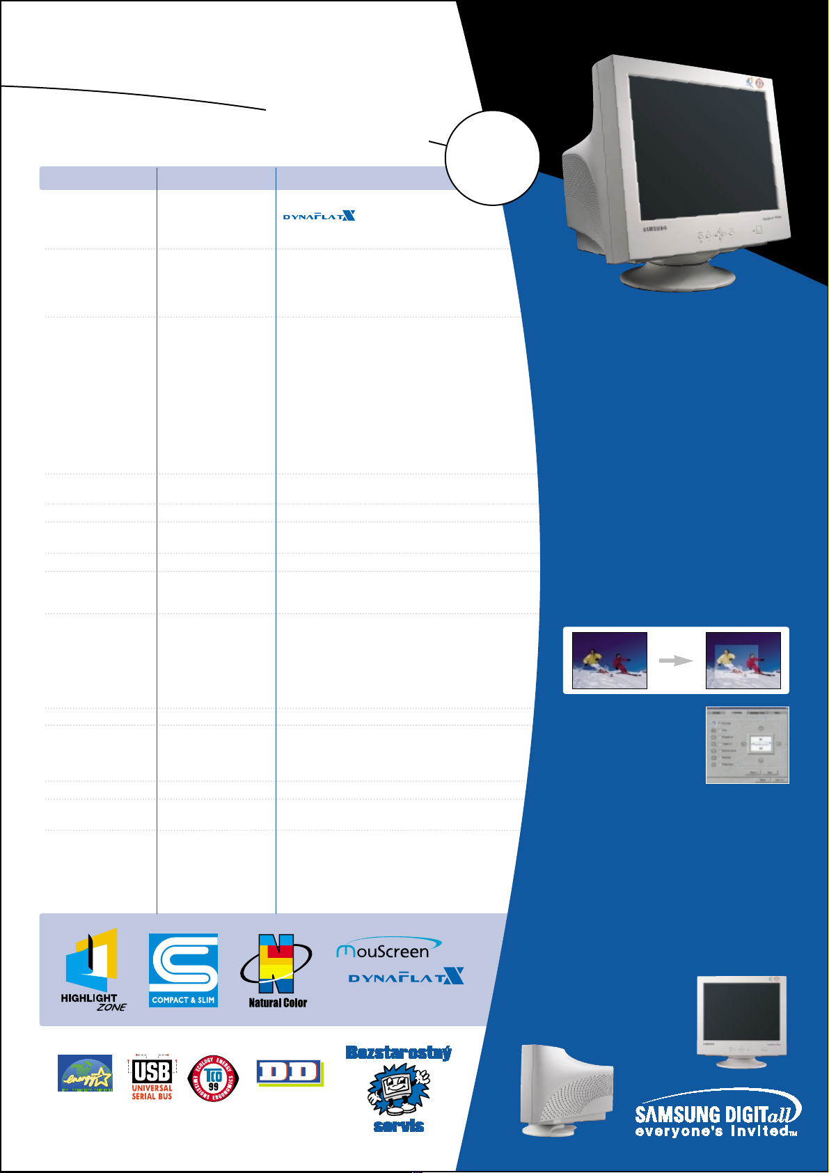
SyncMaster 757DFX využívá nejpokročilejší tech-
nologii SuperCXO (Super Common Extended filed
Oval lens) pro ostřejší zaměření paprsku v nové
ultraploché obrazovce DynalFlat X™.
■■
Podporuje maximální rozlišení 1920x1440
při 64Hz
■■
Highlight Zone™oživí váš monitor
■■
MouScreen™umožňí pohodlné nastavení
monitoru
■■
HBC-Focus™technologie zajistí jasný,
ostrý obraz
■■
Šetří místo díky Compact & Slim Design
■■
Display Director™umožní různé
digitální nastavení
■■
To co vidíte - vytisknete pomocí software
Natural Color
■■
Multimediální reproduktor integrovaný ve
stojanu (volitelný)
Highlight Zone
zjasňuje specifickou obdélníkovou plochu na
obrazovce.
MouScreen™, je druh aplikace
typu Windows, který umož-
ňuje nastavit monitor bez toho, abyste se dotkli prstem jakéhokoli tlačítka na monitoru.
Nyní s pomocí myši můžete
nastavit obraz skrz USB port.
Monitor SyncMaster 757DFX má kompaktní
vzhled a šetří tak místo na vašem stole, kde je mo-
derním a stylovým doplňkem.
Jemná bodová rozteč, vysoký kontrast, vysoké ob-
novovací frakvence a technologie HBC-Focus
(High voltage Bias Control) jsou zárukou ostrého,
jasného obrazu a živých barev.
Digital Display Director™vám umožní snadné nastave-
ní obrazu, jako je teplota barev, moire, ...atd
Software Natural Color
vat barvy na obrazovce s tištěnými ještě před tím, než je
vyplýtván papír kvůli barevnému porovnávání.
Dokonalý zvuk vám poskytne re-
produktor integrovaný ve stojanu
(volitelný).
™
™
monitoru SyncMaster 757DFX
™
uživateli pomáhá synchronizo-
™
Partner of the Year
Display Director

4 Alignment and Adjustments
This section of the service manual explains how to make permanent adjustments to the monitor.
4-1 Adjustment Conditions
Caution: Changes made without the Softjig are saved only to the user mode settings. As such, the
settings are not permanently stored and may be inadvertently deleted by the user.
4-1-1 Before Making Adjustments
4-1-1 (a) ORIENTATION
When servicing, always face the monitor to the
east.
4-1-1 (b) WARM-UP TIME
The monitor must be on for 30 minutes before
starting alignment. Warm-up time is especially
critical in color temperature and white balance
adjustments.
4-1-1 (c) SIGNAL
Analog, 0.7 Vp-p positive at 75 ohm, internal
termination
Sync: Separate/Composite
(TTL level negative/positive)
Sync-on-Green:
Composite sync 0.3 Vp-p negative
(Video 0.7 Vp-p positive)
4-1-1 (d) SCANNING FREQUENCY
Horizontal: 30 kHz to 96 kHz (Automatic)
Vertical: 50 Hz to 160 Hz (Automatic)
Unless otherwise specified, adjust at the
1024 x 768 mode (H: 68 kHz, V: 85 Hz) signals.
Refer to Table 2-1 on pages 2-2 and 2-3.
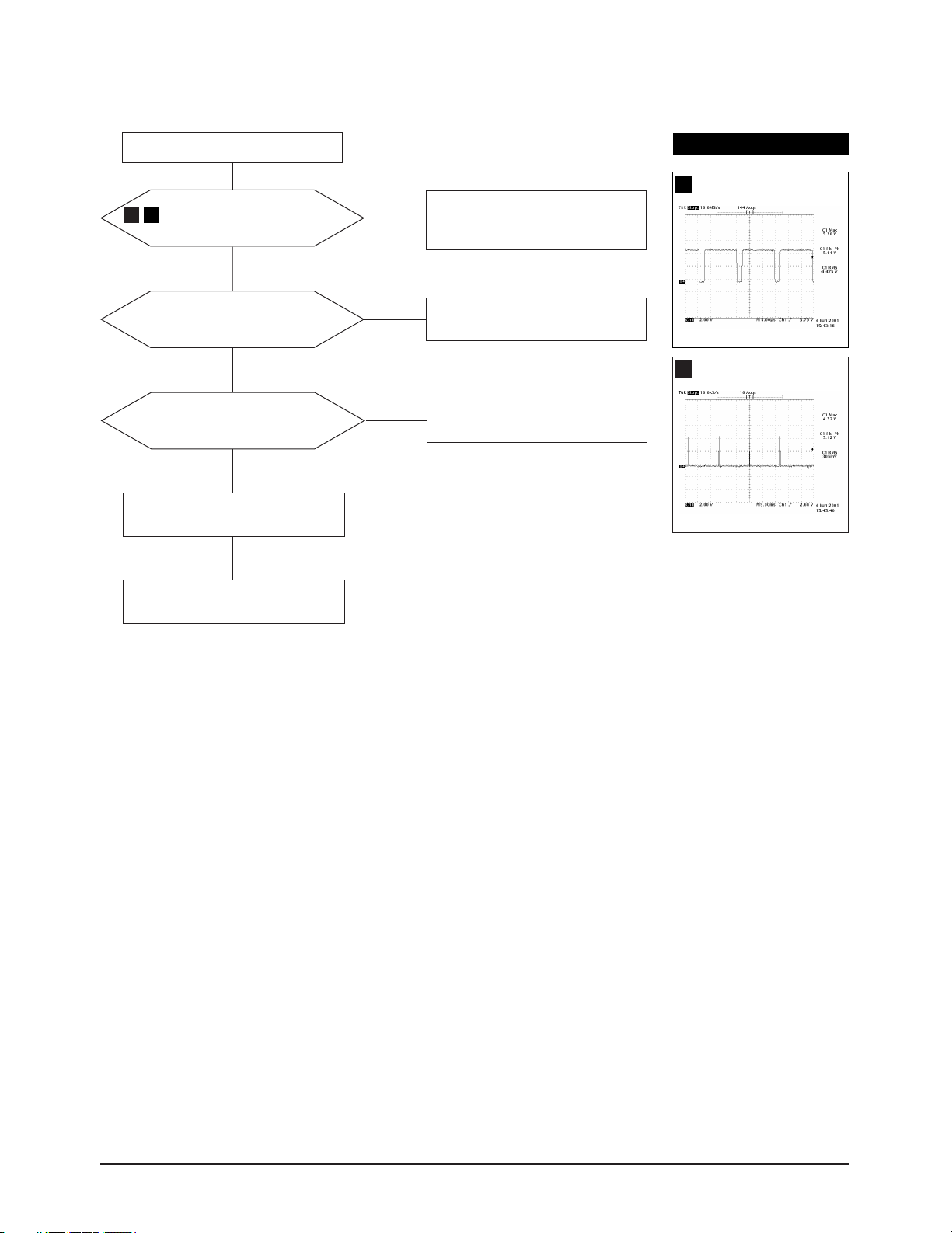
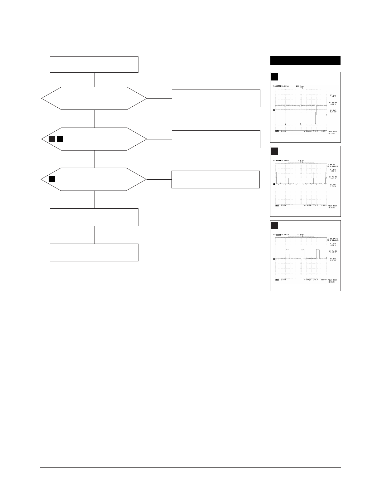
4-1-1 (e) HIGH VOLTAGE ADJUSTMENT
Signal: 1024 x 768 mode (68 kHz/85 Hz)
Display image: Full white
Contrast: Maximum
Brightness: Maximum
Limit: 26 kV ± 0.5 kV
(19”: 27 kV ± 0.5 kV)
Measure the hight voltage level at the anode cap.
High voltage should be within the limit as above.
If the high voltage needs adjustment use the
Softjig.
4-1-1 (f) G2 (SCREEN) VOLTAGE
The Screen Voltage is fixed in the firm so don’t
need to adjust the Screen voltage.
4-1-1 (g) CENTER RASTER
Adjust VR401 so that the back raster comes to the
center when you apply a signal of 91 kHz/85 Hz.
4-1-2 Required Equipment
The following equipment may be necessary for
adjustment procedures:
4-1-2 (a) DISPLAY CONTROL ADJUSTMENT
1. Non-metallic (–) screwdriver: 1.5 mm
Non-metallic (–) screwdriver: 3 mm
2. Philips (+) screwdriver: 1.5 mm
3. Non-metallic hexkey: 2.5 mm
4. Digital Multimeter (DMM), or
Digital Voltmeter (DVM)
5. Signal generator, or
Computer with a video board that uses the
ET-4000 chipset (strongly recommended if
using Samsung DM 200 software) and that
displays: 1280 x 1024 @ 85 Hz, or 1600 x 1200
@ 85 Hz (maximum).
6. Personal computer
4-1-2 (b) COLOR ADJUSTMENTS
1. All equipment listed in 4-1-2 (a), above
2. Color analyzer, or any luminance
measurement equipmen
4-1-3 After Making Adjustments
After finishing all adjustments, test the monitor in
all directions. If, for example, the monitor does not
meet adjustment specifications when facing north,
reposition the monitor to face east and readjust.
This time, try for an adjustment closer to the ideal
setting within the tolerance range. Test the unit
again in all directions. If the monitor again fails to
meet specifications in every direction, contact
your Regional After Service Center for possible
CRT replacement.
❇ Adjust the screen VR of FST so that the G2 (screen) voltage it is 540 ± 10V (AQ19FS)
AQ17HS/AQ17IS/AQ17NS
AQ19MS/AQ19IS/AQ19NS/AQ19FS
4-1
4 Alignment and Adjustments
4-2 Display Control Adjustments
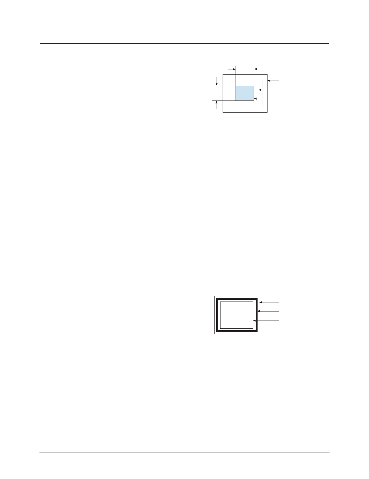
4-2-1 Centering
Centering means to position the center point of
the display in the middle of the display area.
Horizontal size and position and vertical size and
position control the centering of the display.
Adjust the horizontal size and vertical size to their
optimal settings: 312 mm (H) x 234 mm (V).
1024 x 768 mode (68 kHz/85Hz)
Adjust the horizontal position and vertical
position to ≤ 4.0 mm of the center point of the
screen.
|A-B| ≤ 4.0 mm. |C-D| ≤ 4.0 mm.
C
DISPLAY AREA
A
D
Figure 4-3. Centering
4-2-1 (a) HORIZONTAL SIZE ADJUSTMENT
CONDITIONS
Scanning frequency: 68 kHz/85 Hz
Display image: Crosshatch pattern
Brightness: Cut-off
Contrast: Maximum
Click on the << or >> box next to SIZE B+ to
adjust the horizontal size of the display pattern
to 312 mm (Tolerance: ± 3 mm) as the “H_SIZE”
is “60” on the OSD.
4-2-1 (b) VERTICAL SIZE ADJUSTMENT
CONDITIONS
Scanning frequency: 68 kHz /85 Hz
Display image: Crosshatch pattern
Brightness: Cut-off
Contrast: Maximum
Click on the << or >> box next to V_SIZE to
adjust the vertical size of the display pattern to
234 mm. (Tolerance: ± 3 mm.)
4-2-1 (c) HORIZONTAL POSITION ADJUSTMENT
CONDITIONS
Scanning frequency: 68 kHz/85 Hz
Display image: Crosshatch pattern
Brightness: Cut-off
Contrast: Maximum
Click on the << or >> box next to H_POSI to
center the horizontal image on the raster.
B
EDGE OF BEZEL
4-2-1 (d) VERTICAL POSITION ADJUSTMENT
CONDITIONS
Scanning frequency: 68 kHz/85 Hz
Display image: Crosshatch pattern
Brightness: Cut-off
Contrast: Maximum
Click on the << or >> box next to V_POSI to
center the vertical image on the raster.
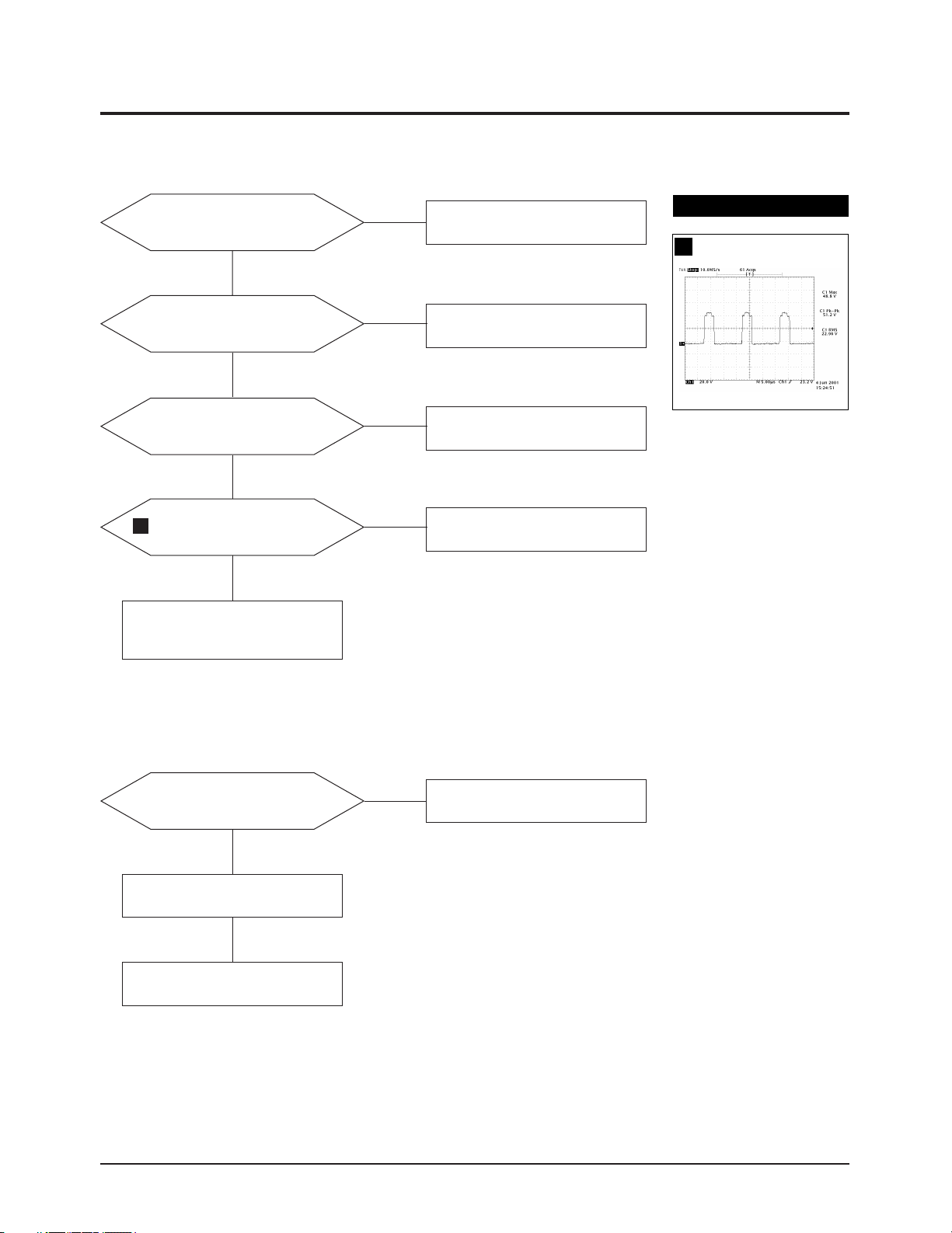
4-2-2 Linearity
Linearity affects the symmetry of images as they
appear on the screen. Unless each row or column
of blocks in a crosshatch pattern is of equal size,
or within the tolerances shown in Table 4-1 an
image appears distorted, elongated or squashed.
Horizontal Linearity = 2x x100
Vertical Linearity = 2x x100
Preset mode
Pre-load mode (48kHz~) ≤ 5% ≤ 10%
Pre-load mode (under 48kHz) ≤ 5% ≤ 14%
❈ Preset Mode : 68KHz / 85Hz
Pre-load Mode : Refer to Timing Chart
4-2-2 (a) HORIZONTAL LINEARITY ADJUSTMENT
CONDITIONS
Scanning frequency: 68 kHz/85 Hz
Display image: Crosshatch pattern
Brightness: Cut-off
Contrast: Maximum
To adjust the Horizontal Linearity, refer to Table
4-1 for the tolerance range.
Click on the << or >> box next to H_LIN to
optimize the image.
(Horizontal x Vertical Size Table)
Horizantal 312 352
Vertical 234 264
X max-X min
X max+X min
Y max-Y min
Y max+Y min
Table 4-1
Adjacent Linearity
≤ 4% ≤ 8%
Table 4-2
17” 19”
Entire Linearity
4-2 AQ17HS/AQ17IS/AQ17NS
AQ19MS/AQ19IS/AQ19NS/AQ19FS
4-2-2 (b) VERTICAL LINEARITY ADJUSTMENT
CONDITIONS
Scanning frequency: 68 kHz/85 Hz
Display image: Crosshatch pattern
Brightness: Cut-off
Contrast: Maximum
To adjust the Vertical Linearity, refer to Table 4-1
for the tolerance range.
Use control bar after selecting “V_LINEARITY
BAL” in left menu to optimize the image.
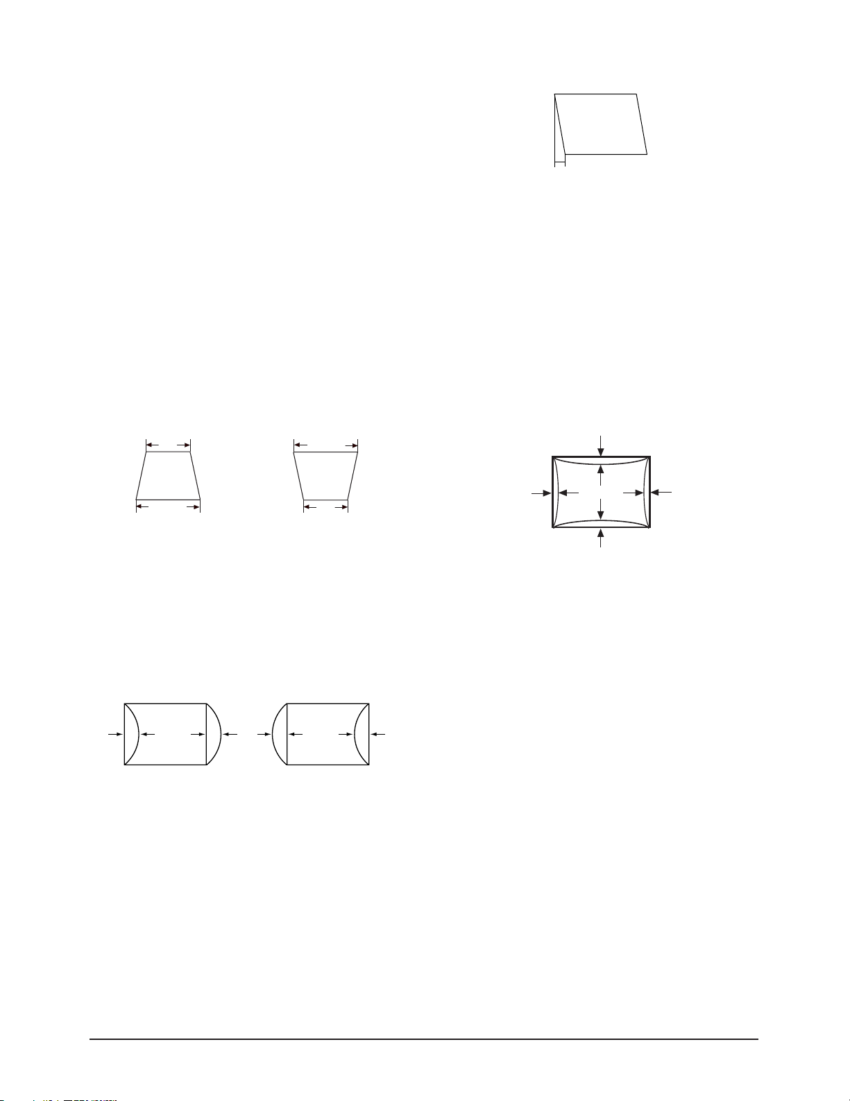
4-2-3 Trapezoid Adjustment
CONDITIONS
Scanning frequency: 68 kHz/85 Hz
Display image: Crosshatch pattern
Brightness: Cut-off
Contrast: Maximum
Use control bar after selecting “TRAPEZOID” in
left menu to make the image area rectangular.
| A - B | < 5 mm
A
A
4 Alignment and Adjustments
4 mm
Figure 4-6. Parallelogram
4-2-6 Side Pincushion Adjustment
CONDITIONS
Scanning frequency: 68 kHz/85 Hz
Display image: Crosshatch pattern
Brightness: Cut-off
Contrast: Maximum
Use control bar after selecting “PINCUSHION” in
left menu to straighten the sides of the image area.
| C1 |, | C2 | ≤ 2.0 mm, | D1 |, | D2 | ≤ 2.0 mm.
C2
B
Figure 4-4. Trapezoid
B
4-2-4 Pinbalance Adjustment
CONDITIONS
Scanning frequency: 68 kHz/85 Hz
Display image: Crosshatch pattern
Brightness: Cut-off
Contrast: Maximum
| D1 |, | D2 | ≤ 2.0 mm
D1 D2 D1
Figure 4-5. Pinbalance
Use control bar after selecting “PINBALANCE” in
left menu to optimize the image.
4-2-5 Parallelogram Adjustment
CONDITIONS
Scanning Frequency: 68 kHz/85 Hz
Display image: Crosshatch pattern
Brightness: Cut-off
Contrast: Maximum
Use control bar after selecting “PARALLEL” in
left menu to make the image area rectangular.
D2D1
C1
Figure 4-7. Pincushion
4-2-7 Degauss
No adjustments are available for the degaussing
circuit. The degaussing circuit can effectively
function only once per 30 minutes.
4-2-8 Save the Data
To save the adjustment data for factory
frequencys, press FACTORY SAVE.
4-2-9 To Delete the User Mode Data
To delete the adjustment data from the user
modes, click “@4: USER DELETE” in right menu.
AQ17HS/AQ17IS/AQ17NS
AQ19MS/AQ19IS/AQ19NS/AQ19FS
4-3
4 Alignment and Adjustments
4-3 Color Adjustments
4-3-1 Color Coordinates (Temperature)
Color temperature is a measurement of the
radiant energy transmitted by a color. For
computer monitors, the color temperature refers
to the radiant energy transmitted by white. Color
coordinates are the X and Y coordinates on the
chromaticity diagram of wavelengths for the
visible spectrum.
CONDITIONS
Measurement instrument: Color analyzer
Scanning frequency: 68 kHz/85 Hz
Display Size : 312 (H) x 234 (V)
Display image: White flat field at
center of display area
Brightness: Cut-off
Contrast: Maximum
PROCEDURE
Use the directions in sections 4-3-2 through 4-3-4
to adjust the color coordinates for:
9300K to x = 0.283 ± 0.02, y = 0.298 ± 0.02
6500K to x = 0.313 ± 0.02, y = 0.329 ± 0.02
5000K to x = 0.346 ± 0.02, y = 0.359 ± 0.02
4-3-2 (b) G-GAIN ADJUSTMENT
1/3H-1/2H
FRONT BEZEL OPENING
1/3V-1/2V
BACK RASTER
GREEN WINDOW
Figure 4-8. Green Box Pattern
CONDITIONS
Scanning frequency: 68 kHz/85 Hz
Display image: Green box pattern
Brightness: Cut-off
Contrast: Maximum
1. Click on the << or >> box next to G_GAIN to
adjust the brightness of the Green Gain to
40 ± 1 ft-L.
2. Click on the << or >> box next to “BM
Contrast” to adjust the Brightness of the High
Light Gain to 75ft-L when the High Light
function was (“BM contrast” Menu is in the
“Extra Menu”) activated with Maximum size.
4-3-2 Color Adjustments for 9300K
4-3-2 (a) BACK RASTER COLOR ADJUSTMENT
CONDITIONS
Scanning frequency: 68 kHz/85 Hz
Display image: Back raster pattern
Brightness: Cut-off
Contrast: Maximum
1. Select COLOR CHANNEL 1 to control the
color for 9300K.
2. Adjust the luminance of the back raster to
between 0.5 to 0.7ft-L using the “GREEN
CUTOFF” controls.
3. Use control bar after selecting “BLUE
CUTOFF” in left menu to set the “y”
coordinate to 0.298 ± 0.015
4. Use control bar after selecting “RED
CUTOFF” in left menu to 0.283 ± 0.015
* If color values would not be matched desirable
values, repeat sequence 3 and 4 after readjusting
“GREEN CUTOFF” control a little different.
4-3-2 (c) WHITE BALANCE ADJUSTMENT
CONDITIONS
Scanning frequency: 68 kHz/85 Hz
Display image: Full white pattern
Brightness: Cut-off
Contrast: Maximum
FRONT BEZEL OPENING
BACK RASTER
WHITE WINDOW
Figure 4-9. Full White Pattern
1. Click on the << or >> boxes next to R_GAIN
and B_GAIN to make the video white.
(For 9300K color adjustment:
x = 0.283 ± 0.02, y = 0.298 ± 0.02.)
Note: Do not touch the G_GAIN controls.
2. Check the ABL. If it is not within the
specifications (30 ± 1 ft-L), use the ABL
controls to adjust it.
3. Select COLOR FACTORY SAVE to save the
data.
4-4 AQ17HS/AQ17IS/AQ17NS
AQ19MS/AQ19IS/AQ19NS/AQ19FS
4 Alignment and Adjustments
Luminance Table (9300K) 4-3
17HS/IS/NS
Without ABL 40ft-L 36ft-L 36ft-L
Without ABL 31ft-L 30ft-L 30ft-L
Without ABL
(High Light is Activated)
75ft-L 75ft-L 65ft-L
19MS/NS/FS
19IS
4-3-2 (d) WHITE BALANCE ADJUSTMENT VERIFICATION
CONDITIONS
Scanning frequency: 68 kHz/85 Hz
Display image: Back raster pattern
X-Y Coordinates: x = 0.283 ± 0.02,
y = 0.298 ± 0.02
Raster Luminance 0.3 ~ 1ft-L
ABL Luminance 30 ± 1 ft-L
Brightness: Cut-off
Contrast: Maximum
1. Check whether the color coordinates of the
back raster satisfy the above spec.
If they do not, return to 4-3-2 (a) and readjust
all settings.
2. Display a full white pattern.
4-3-3 (b) G-GAIN ADJUSTMENT
This procedure is the same as that for 9300K, refer
to the procedure on page 4-5.
You must adjust the Brightness of Green gain to
39 ± 1ft-L.
4-3-3 (c) WHITE BALANCE ADJUSTMENT
CONDITIONS
Scanning frequency: 68 kHz/85 Hz
Display image: Full white pattern
Brightness: Cut-off
Contrast: Maximum
1. Click on the << or >> boxes next to R_GAIN
and B_GAIN to make the video white.
(For 6500K color adjustment:
x = 0.313 ± 0.02, y = 0.329 ± 0.02.)
2. Refer to the procedure for 9300K, section
4-3-2 (c) steps 2 and 3.
4-3-3 (d) WHITE BALANCE ADJUSTMENT VERIFICATION
Refer to the procedure for 9300K, section 4-3-2 (d).
Luminance Table (6500K) 4-4
Note: Do not touch the G_GAIN controls.
3. Adjust the Contrast Control on the monitor so
that the luminance of the video is about 5 ft-L.
4. Check whether the white coordinates of the
video meet the above coordinates spec.
5. Adjust the Contrast Control again so that the
luminance of the video is about 20 ft-L.
6. Check whether the white coordinates of the
video satisfies the above spec.
If they do not, return to 4-3-2 (a) and readjust
all settings.
4-3-3 Color Adjustments for 6500K
4-3-3 (a) BACK RASTER COLOR ADJUSTMENT
CONDITIONS
Scanning frequency: 68 kHz/85 Hz
Display image: Back raster pattern
Brightness: Cut-off
Contrast: Maximum
1. Select COLOR CHANNEL 2 to control the
color for 6500K.
2. Adjust the luminance of the back raster to
between 0.5 to 0.7 ft-L using the G_CUT
controls.
3. Click on the << or >> boxes next to R_CUT
and B_CUT to adjust the R-Bias to x = 0.313 ±
0.02 and the B-Bias to y = 0.329 ± 0.02.
17HS/IS/NS 19NS/FS/IS
Without ABL 39ft-L 34ft-L
With ABL 30ft-L 29ft-L
4-3-4 Color Adjustments for 5000K
4-3-4 (a) BACK RASTER COLOR ADJUSTMENT
CONDITIONS
Scanning frequency: 68 kHz/85 Hz
Display image: Back raster pattern
Brightness: Cut-off
Contrast: Maximum
1. Select COLOR CHANNEL 3 to control the
color for 5000K.
2. Adjust the luminance of the back raster to
between 0.5 to 0.7 ft-L using the G_CUT
controls.
3. Click on the << or >> boxes next to R_CUT
and B_CUT to adjust the R-Bias to x = 0.346 ±
0.02 and the B-Bias to y = 0.359 ± 0.02.
4-3-4 (b) G-GAIN ADJUSTMENT
This procedure is the same as that for 9300K, refer
to the procedure on page 4-5.
Adjust the brightness of the G_GAIN less 2 ft-L
than brightness of procedure for 9300K.
4-3-4 (c) WHITE BALANCE ADJUSTMENT
AQ17HS/AQ17IS/AQ17NS
AQ19MS/AQ19IS/AQ19NS/AQ19FS
4-5
4 Alignment and Adjustments
CONDITIONS
Scanning frequency: 68 kHz/85 Hz
Display image: Full white pattern
Brightness: Cut-off
Contrast: Maximum
1. Click on the << or >> boxes next to R_GAIN
and B_GAIN to make the video white.
(For 5000K color adjustment:
x = 0.346 ± 0.02, y = 0.359 ± 0.02.)
2. Refer to the procedure for 9300K, section
4-3-2 (c) steps 2 and 3.
Luminance Table (6000K) 4-5
17HS/IS/NS 19NS/FS/IS
Without ABL 38ft-L 33ft-L
With ABL 30ft-L 28ft-L
4-3-4 (d) WHITE BALANCE ADJUSTMENT VERIFICATION
Refer to the procedure for 9300K, section 4-3-2 (d).
4-3-5 Luminance Uniformity Check
Luminance is considered uniform only if the ratio
of lowest to highest brightness areas on the screen
is not less than 7.5:10.
CONDITIONS
Scanning frequency: 68 kHz/85 Hz
(1024 x 768)
Display image: White flat field
Display size 312 (H) x 234 (V)
Brightness: Cut off point
Contrast: Maximum
PROCEDURE
Measure luminance at nine points on the display
screen (see figure below).
PROCEDURE
1. Adjust the Focus VR on the FBT to display the
sharpest image possible.
2. Use Locktite to seal the Focus VR in position.
4-3-7 Color Purity Adjustment
Color purity is the absence of undesired color.
Conspicuous mislanding (unexpected color in a
uniform field) within the display area shall not be
visible at a distance of 50 cm from the CRT
surface.
CONDITIONS
Orientation: Monitor facing east
Scanning frequency: 68 kHz/85 Hz
Display image: White flat field
Luminance: Cut off point at the center
of the display area
Note: Color purity adjustments should only be
attempted by qualified personnel.
PROCEDURE
For trained and experienced service technicians
only.
Use the following procedure to correct minor
color purity problems:
1. Make sure the display is not affected by
external magnetic fields.
2. Very carefully break the glue seal between the
2-pole purity convergence magnets (PCM), the
band and the spacer.
3. Make sure the spacing between the PCM
assembly and the CRT stem is 29 mm ± 1 mm.
4. Display a green pattern over the entire display
area.
5. Adjust the purity magnet rings on the PCM
assembly to display a pure green pattern.
(Optimum setting: x = 0.295 ± 0.015,
y = 0.594 ± 0.015)
6. Repeat steps 4 and 5 using a red pattern and
then again, using a blue pattern.
Figure 4-10 Luminance Uniformity Check Locations
4-3-6 Focus Adjustment
CONDITIONS
Red: x = 0.620 ± 0.015 y = 0.334 ± 0.015
Green: x = 0.289 ± 0.015 y = 0.595 ± 0.015
Blue: x = 0.153 ± 0.015 y = 0.072 ± 0.015
Table 4-6. Color Purity Tolerances
Scanning frequency: 68 kHz/85 Hz
Display image: “H” character pattern
Brightness: Cut off point
Contrast: Maximum
(For 9300K color adjustment: x = 0.283 ± 0.02, y = 0.298 ± 0.02)
7. When you have the PCMs properly adjusted,
carefully glue them together to prevent their
movement during shipping.
4-6 AQ17HS/AQ17IS/AQ17NS
AQ19MS/AQ19IS/AQ19NS/AQ19FS
5 Troubleshooting
5-1 Parts Level Troubleshooting
Notes: 1. If a picture does not appear, Click the Brightness and Contrast button on the front panel, and then increase the value
of Brightness and Contrast.
2. Check the following circuits.
• No raster appears: Power circuit, Horizontal output circuit, H/V control circuit, and H/V output circuit.
• High voltage develops but no raster appears: Video output circuits.
• High voltage does not develop: Horizontal output circuits.
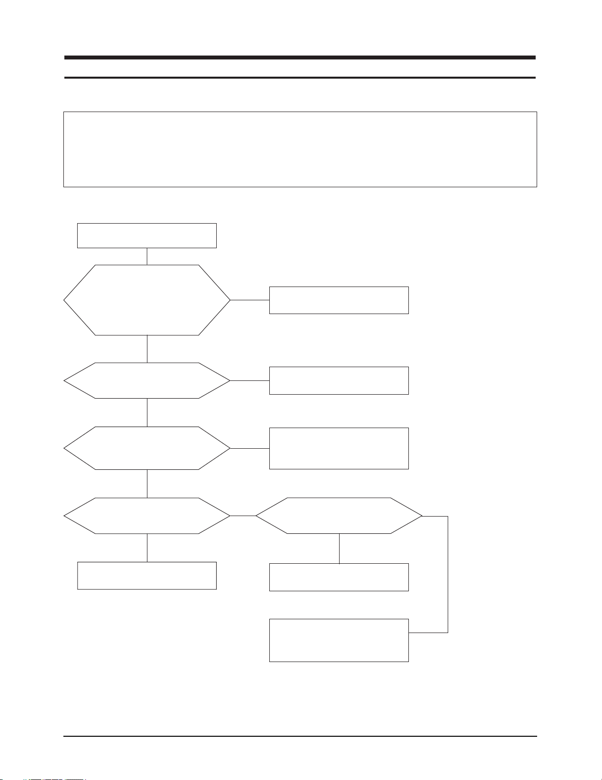
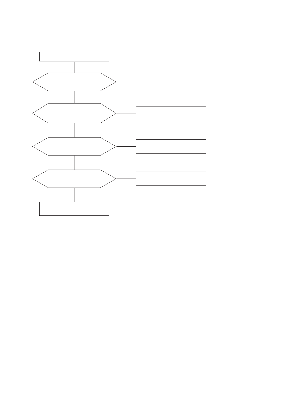
5-1-1 No Power Supply
Check and replace FG601, D601,
D701, Q701, IC601 and ZD601.
Check the Voltage at
C607 plus polarity point.
Is the Voltage 400VDC?
with PFC : 400VDC
without PFC : it is different
according to input voltage
Yes
No
Check and replace
FG601, D601, D703.
IC601 Pin 1 waveform is right?
Yes
The secondary voltage of
T601 is right?
(Is it same the schemetic diagram)
Yes
Check IC651 (KA78R12) Pin 12?
•
Is the voltage 12VDC?
•
Yes
Done.
No
No
No
Check and replace
IC601, ZD601, D606, IC701.
Check TR, IC and biode
related to every B+line.
Appear 4VDC Pin 4 of IC651?
No
Check and Micom. (IC201)
•
Check and replace IC651.
•
Check every IC connected to 12V.
Yes
AQ17HS/AQ17IS/AQ17NS
AQ19MS/AQ19IS/AQ19NS/AQ19FS
5-1
5 Troubleshooting
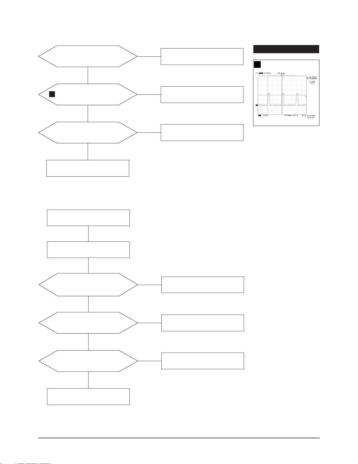
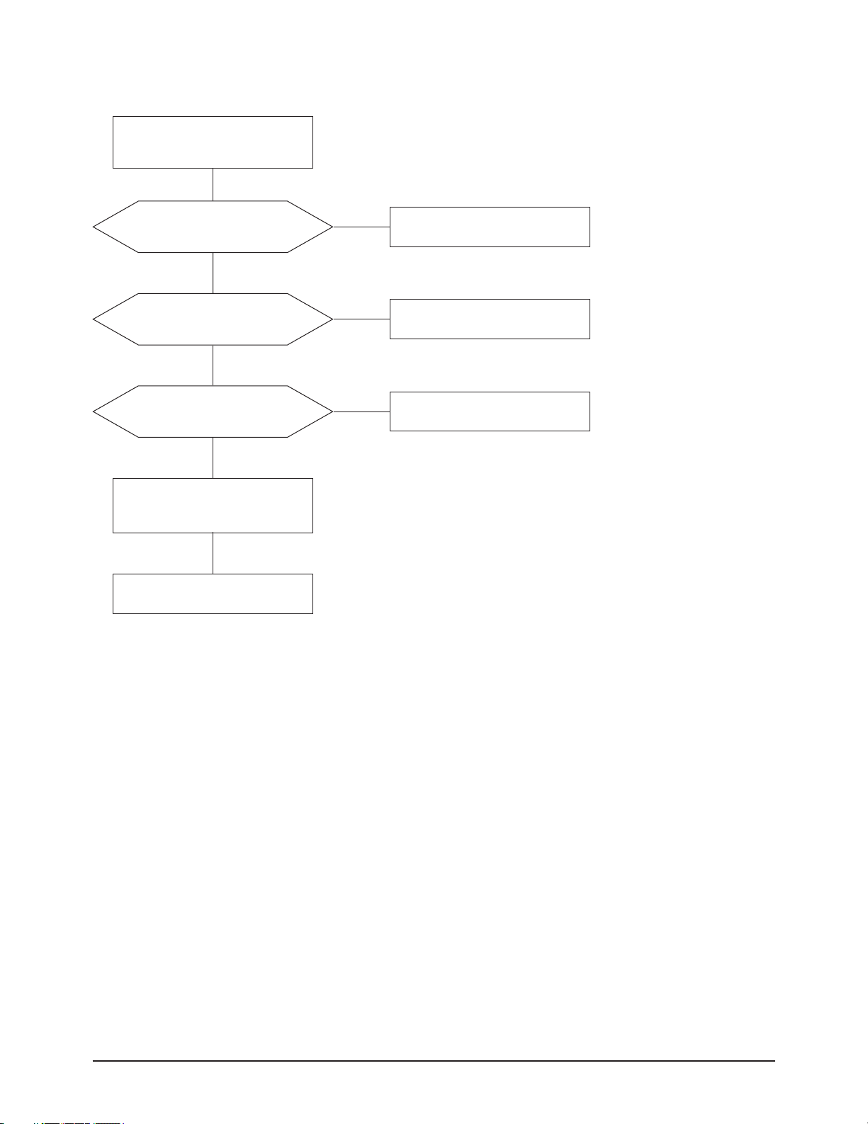
5-1-2 PFC Failure
Check the Voltage at IC701 Pin5.
The Voltage is around 10VDC?
Yes
1
Q701 Gate waveform is right?
Yes
Check the Voltage at D701 cathode.
The Voltage is about 400VDC?
Yes
Done.
5-1-3 DPMS Failure
Check signal source
H/V sync. video signal.
No
No
No
Check and Replace D702,
R711, ZD705, ZD706.
Replace IC701.
Replace Q701, D701.
WAVEFORMS
368 V (IC601, #1)
1
Make No H/V sync.
( That is power off mode).
LED blinks?
Does +12V Line off?
(Check the IC651 output Pin 2)
Yes
Does +14V_V Line off?
(Check the Q670 Collector)
Yes
Does the Q620 activate?
Yes
Done.
No
No
No
Check IC201 Pin 25
or replace IC201.
Check Q671, D670.
Check IC201 Pin 23
or replace IC201.
5-2 AQ17HS/AQ17IS/AQ17NS
AQ19MS/AQ19IS/AQ19NS/AQ19FS
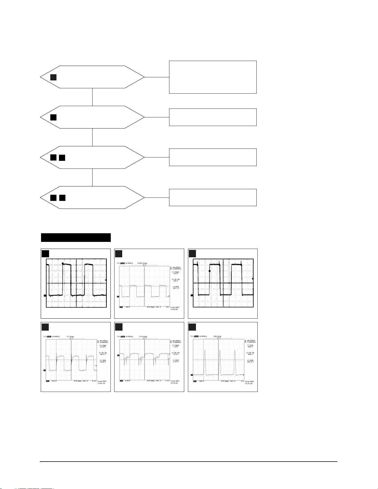
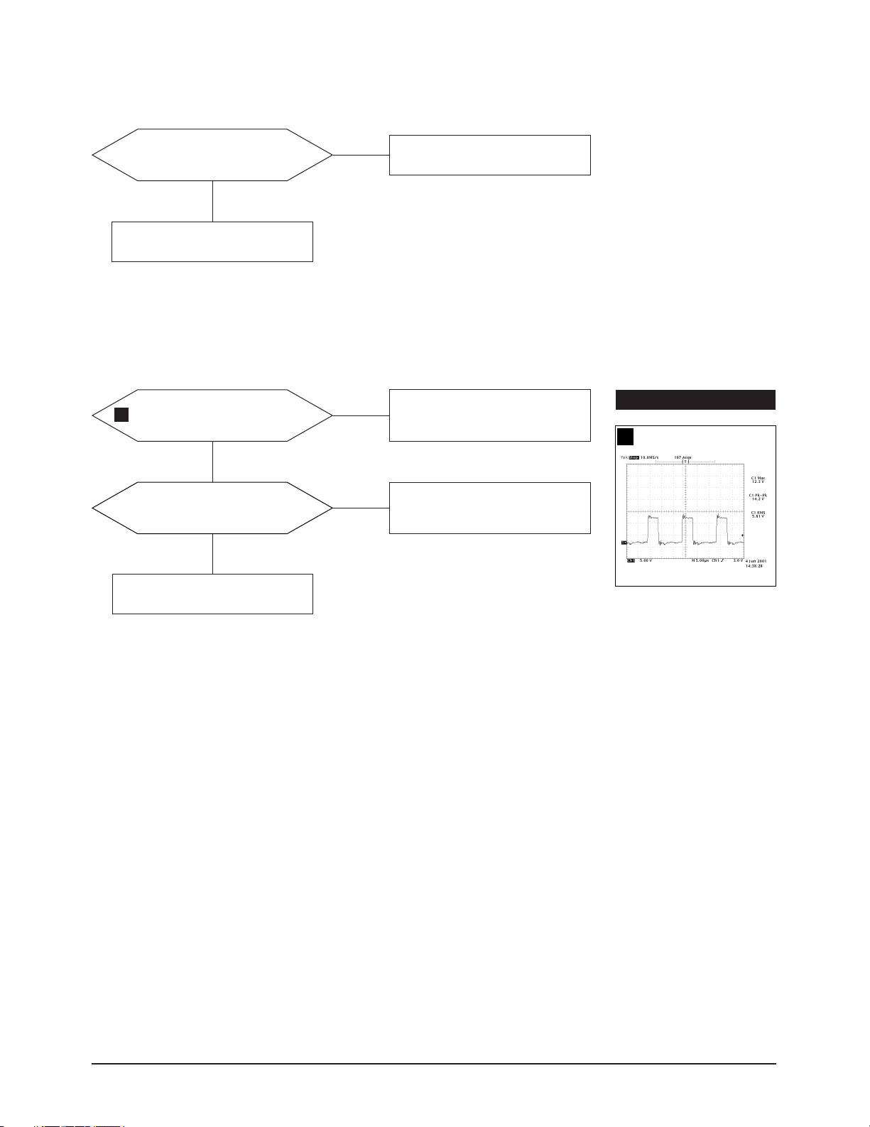
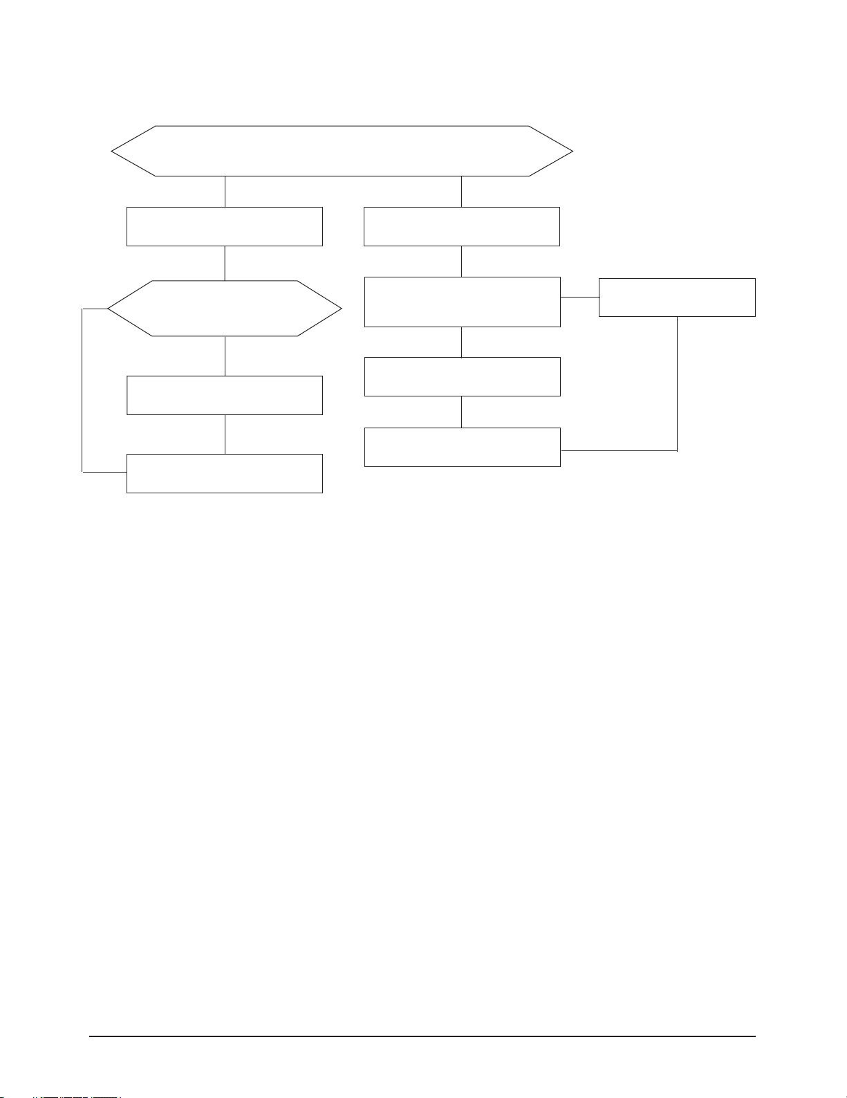
5-1-4 H_Deflection Failure
5 Troubleshooting
IC402 Pin 6 waveform is right?
2
Yes
3
Q454 drain
waveform is right?
Yes
4
Q401 gate, drain
5
waveforms are right?
Yes
Q402 base, collector
6
7
waveforms are right?
WAVEFORMS
No
No
No
No
1. Appear the Voltage 12VDCat
IC402 Pin 7 replace R451.
2. Check IC402 Pins 6~5, 7~6.
3. Replace IC402.
Check Q451, Q452, Q453,
ZD450, R467, D456.
Check Q250, Q251, IC250
Check +19V line.
Check and replace D402 and Q402.
Check DY connector connection.
IC402, #6
2
CH1 P-P = 10.96 V CH1 RMS = 6.180 V
Q401, Drain
5
Q454, Drain
3
Q402, Base
6
Q401, Gate
4
CH1 P-P = 11.6 V CH1 RMS = 6.944V
Q402, Collector
7
AQ17HS/AQ17IS/AQ17NS
AQ19MS/AQ19IS/AQ19NS/AQ19FS
5-3
5 Troubleshooting
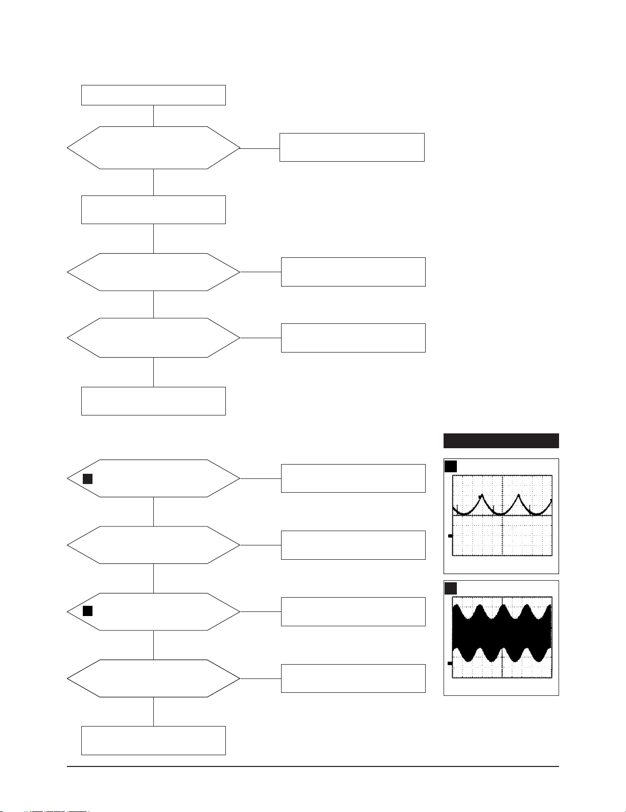
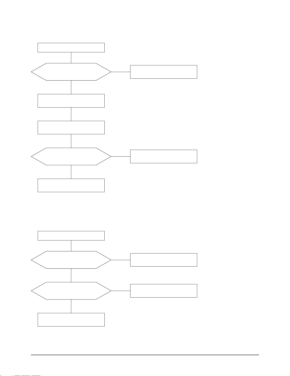
5-1-5 S Correction Failure
Check S1 ~ S5 signal.
Refer to the S-corrction table page?
S1~S5 signals are right at
each frequency block?
Yes
Check and replace
C411, C413, C414, C415, C416,
C417, C418, Q403 ~ Q407, Q408 ~ Q412
5-1-6 H_Lin. Failure
IC201 Pin 3 voltage varies with
different H_Lin. DAC values?
Yes
IC403 Pin 7, 8 voltage varies with
different H_Lin. DAC values?
Yes
No
No
No
Check and replace IC201.
Replace IC201.
Check +12 V line.
Check some parts around IC403.
Check L403.
5-1-7 Invariable H_Size
D250 Cothode voltage varies with
different H_Size DAC values?
Yes
IC402 Pin 6 output duty varies with
different H_Size DAC values?
No
No
Check and replace IC250, IC201.
Check some parts
around IC250, IC201.
5-4 AQ17HS/AQ17IS/AQ17NS
AQ19MS/AQ19IS/AQ19NS/AQ19FS
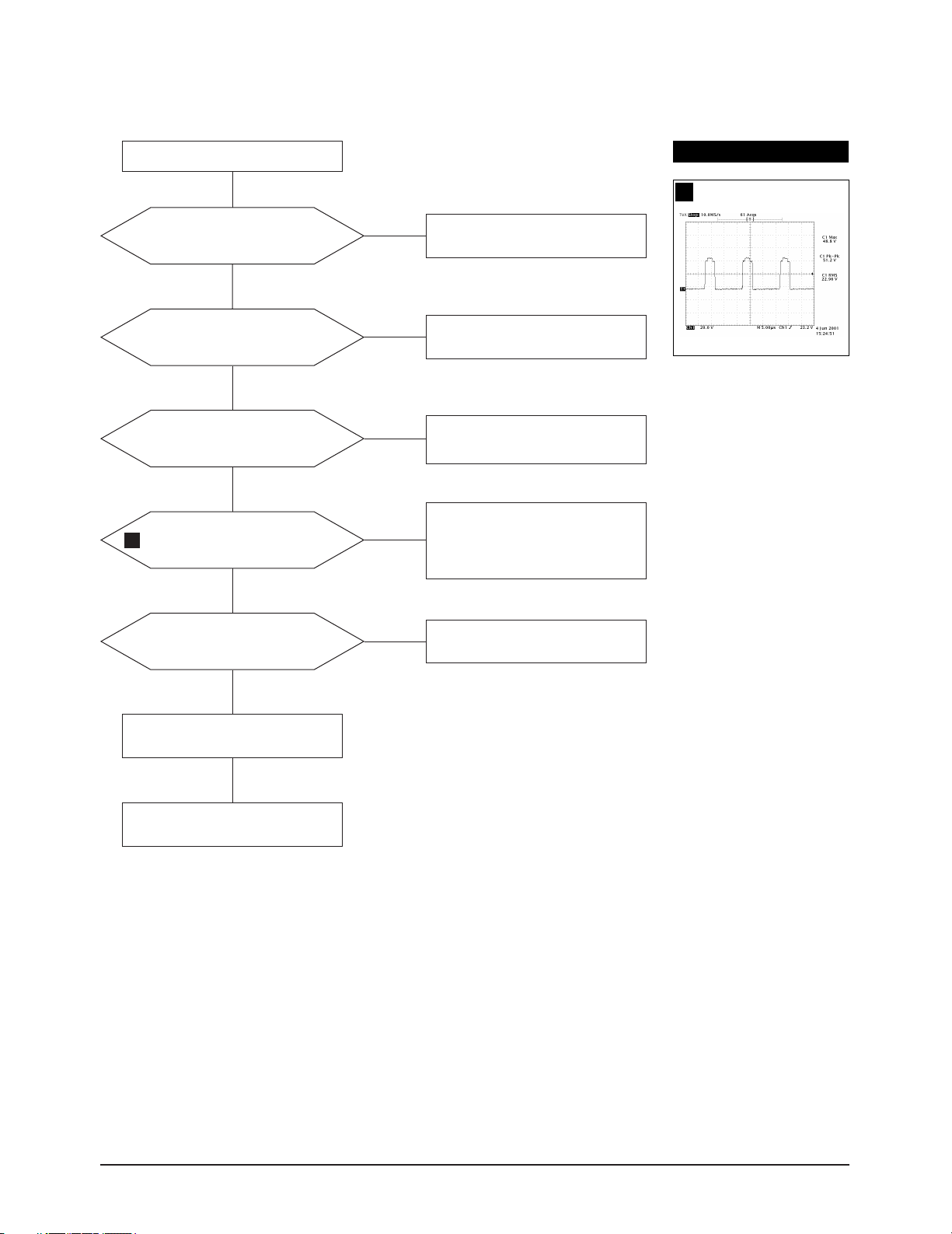
5-1-8 Abnormal H_Size
5 Troubleshooting
WAVEFORMS
The Voltage waveforms at
7
Q402 Collector are right?
Yes
T402 pin 8 wareform is right?
8
Yes
Check some parts around
IC250 and IC402 Pin 1 and 2.
5-1-9 Side Pin or Trap Failure
IC250 Pin 24 output exists?
9
The waveform is right?
Yes
No
No
No
Repeat the troubleshooting
Guide of H_deflection failure.
Replace T402.
Check and replace IC250.
Q402, Collector
7
T402, #8
8
Check and replace IC402.
Check some parts IC402 Pin 2
and IC250 Pin 24.
5-1-10 Para. or Pin Balance Failure
IC250 Pin 24 output varies with
different DAC values?
No
Replace IC261.
WAVEFORMS
IC250, #24
9
AQ17HS/AQ17IS/AQ17NS
AQ19MS/AQ19IS/AQ19NS/AQ19FS
5-5
5 Troubleshooting
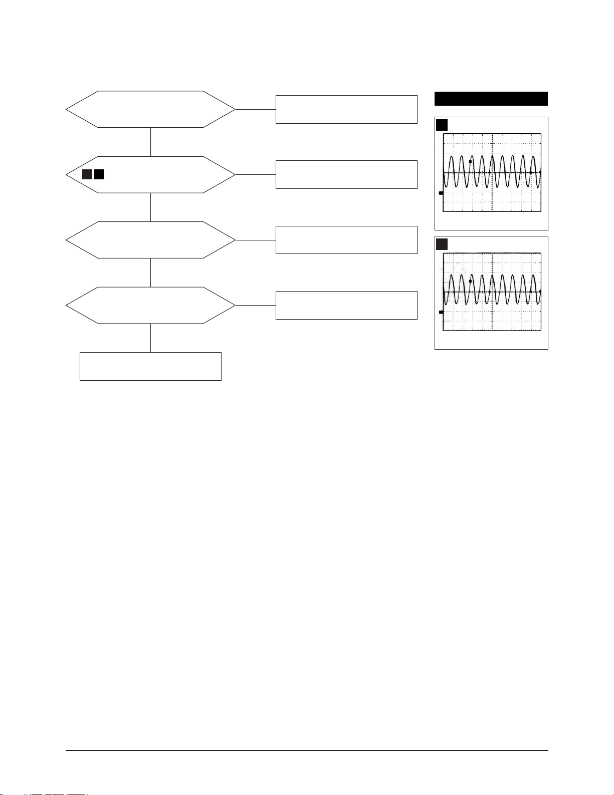
5-1-11 Tilt Failure
Check tilt connector connection
IC201 Pin 5 output duty varies
with different DAC values?
Yes
IC403 Pin 10, 11 output varies with
different DAC values?
Yes
Check and replace CRT.
5-1-12 V Deflection Failure
Is 14V at IC301 Pin 2?
Is -14V at IS301 Pin 5?
Yes
No
No
No
Check and replace IC201.
Check and replace IC403.
Check and replace R312, R316.
Refer to 5-1-1 No Power supply.
WAVEFORMS
IC250, #23
10
IC250 Pin 23 output exists?
10
The waveform is right?
Yes
IC301 Pin 6 output exists?
11
The waveform is right?
Yes
Check V DY connector connection.
No
No
Check and replace IC250.
Check and replace some
parts around IC301.
IC301, #6
11
5-6 AQ17HS/AQ17IS/AQ17NS
AQ19MS/AQ19IS/AQ19NS/AQ19FS
5-1-13 V Size or Pos. Variation Failure
5 Troubleshooting
IC250 Pin 23 output varies with
different DAC values?
Yes
Check and replace IC250 and IC301.
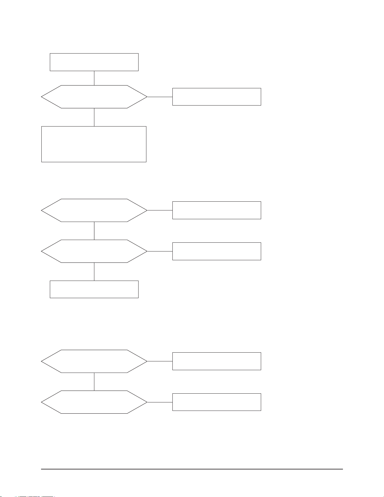
5-1-14 High Voltage Failure
Q504 gate driving pulse exist?
12
The waveform is right?
Yes
Are there some voltages
(350V, 30V, -210V, etc)
at secondary part of FBT?
No
No
No
Check some parts around IC250.
Check bias voltage.
Check +12 V line.
Check and replace
Q502, Q503, R511, IC501.
Check and replace Q504, D508,
D509, D530, D507, D505.
WAVEFORMS
Q504, Gate
12
Done.
Yes
AQ17HS/AQ17IS/AQ17NS
AQ19MS/AQ19IS/AQ19NS/AQ19FS
5-7
5 Troubleshooting
5-1-15 ABL Failure
Input full white pattern to monitor.
IC102 Pin12 (19”: IC101, Pin15)
input exists and
varies with different patterns?
No
Check CN102, Q101, Q102, ZD101.
T501 Pin 8 Voltage exists?
Yes
IC103 Pin 16 output exists and
varies with different patterns?
Yes
Check and replace IC102 and CRT
Yes
Check and replace IC102
No
Check and replace T501.
No
Check and replace IC103.
(19”:IC101)
.
5-1-16 Focus Failure
13
14
IC250 Pin 11 and 32
output are right?
Yes
Some parts around Q551,
Q552, Q553 and Q540 are right?
Yes
Some parts around T502 are right?
Yes
Does the voltage of Q541
collector change as the FH function
is changed on the OSD menu?
Yes
Check the connection between FBT
Pin 13, CRT Socket PCB.
No
Check and replace IC261.
No
Replace failed part.
No
Replace failed part.
No
Check Q541 and others components.
WAVEFORMS
2.20 V (IC250, #11, 32)
13
CH1 P-P = 2.20 V CH1 RMS = 2.776 V
580 V (T501, #1)
14
CH1 P-P = 580 V CH1 RMS = 278.2 V
5-8 AQ17HS/AQ17IS/AQ17NS
AQ19MS/AQ19IS/AQ19NS/AQ19FS
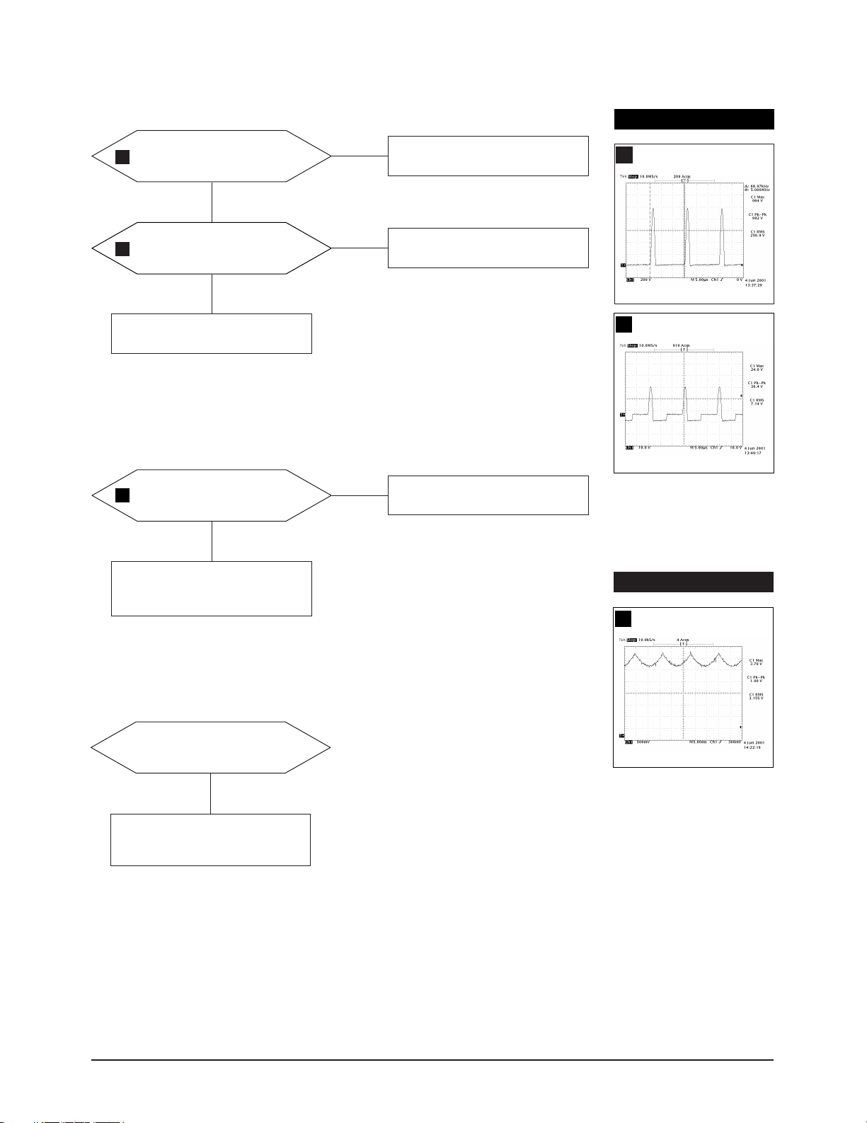
5-1-17 No Video
5 Troubleshooting
Check signal cable and connection.
IC101 Pins 2, 4 and 6 (19”: IC105,
Pins 2, 4 and 6) inputs are right?
Yes
IC101 Pins 20, 22 and 24
(19”: IC105, Pins 20, 22, 24)
outputs are right?
Yes
IC102 Pins 25, 28 and 30
(19”: IC101, 29, 32, 35)
outputs are right?
Yes
Are there waveforms at CRT
15
Socket Pin Red, Green, Blue?
Yes
No
No
No
No
Check CN101, IC1, QR51, QG51,
QB51, and IC3 on BNC Board.
Check Vcc on IC101 (19”: IC105)
and replace IC101 (19”: IC105).
Check +12 V line.
Check and replace IC102 (19”: IC101).
Check +80 V line.
Check and replace IC105
(19”:IC102) and components
around IC105 (19”:IC102).
WAVEFORMS
CRT Socket, Red, Green, Blue
15
G2 voltage is right?
Heater Voltage is right?
Yes
Change CRT.
Done.
No
Check D598, D599 and G2 wire.
Check CN102 wire Assy.
AQ17HS/AQ17IS/AQ17NS
AQ19MS/AQ19IS/AQ19NS/AQ19FS
5-9
5 Troubleshooting
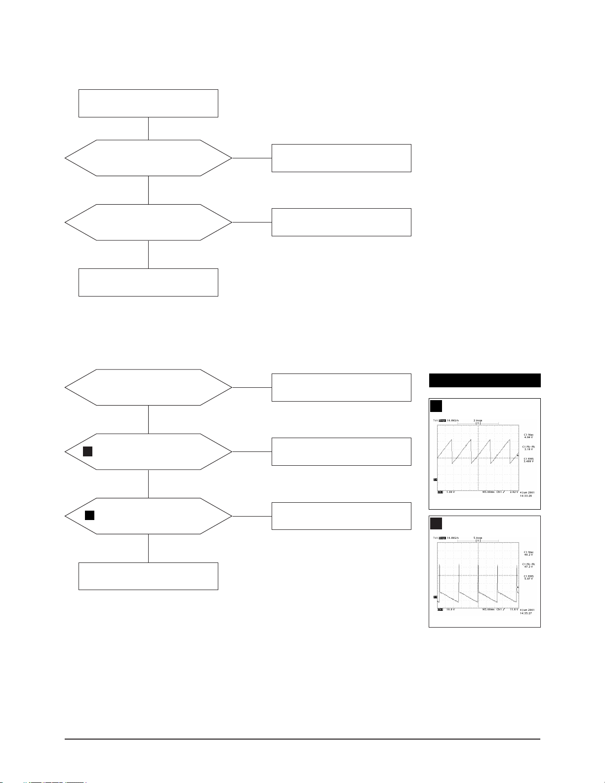
5-1-18 Micom Failure
IC201 Pin 13 input is over 4.2V?
Yes
16 17
IC201 Pin 32 and 33
inputs are right?
Yes
IC201 Pin 40 input is High Active?
Yes
All in/output values are right?
Yes
Done.
No
No
No
No
Check IC650.
Check X201, C203 and C204.
Check and replace IC202.
Replace IC201.
WAVEFORMS
3.42 V (IC201, #33)
16
CH1 P-P = 3.42 V CH1 RMS = 2.500V
3.16 V (IC201, #32)
17
CH1 P-P = 3.16 V CH1 RMS = 2.560 V
5-10 AQ17HS/AQ17IS/AQ17NS
AQ19MS/AQ19IS/AQ19NS/AQ19FS
5-1-19 OSD Failure
5 Troubleshooting
Check CN102 and connector Ass’y.
IC103 (19”: IC03) Pin 6 and 17
18 19
waveforms are right?
Is there 5V on IC103 Pin 5 and 24?
Yes
IC102 Pins 1, 2 and 3, 4 (19”: IC101
Pins 1, 4 and 9, 13) input is right?
Yes
Does the Voltage Change on
IC201 Pins 11, 12 When you
push the control Button?
Yes
Check IC201.
No
No
Check and replace IC103 (19”:IC103).
No
Check and replace
Q104, IC201 Pin 20.
Check 5V Line.
Check CN204 and Assy.
WAVEFORMS
IC103, #6, 17
18
IC103, #5, 24
19
Done.
AQ17HS/AQ17IS/AQ17NS
AQ19MS/AQ19IS/AQ19NS/AQ19FS
5-11
5 Troubleshooting
5-1-20 User Control Failure
Check connector Ass’y.
IC201 Pins 11 and 12 inputs are
right at each function?
Yes
Check and replace IC201.
Done.
5-1-21 Degaussing Failure
Check degaussing connector.
RL601 operation is right?
No
Check and replace function key.
Yes
Check D-Coil, POS601.
No
Q601 base input is right?
No
IC201 Pin 31 output is right?
Yes
Done.
Yes
No
Check and replace Q601.
Check and replace IC201.
Check user function key.
5-12 AQ17HS/AQ17IS/AQ17NS
AQ19MS/AQ19IS/AQ19NS/AQ19FS
5-2 General Troubleshooting
5-2-1 No Picture
5 Troubleshooting
LED blinks?
No
G2 Voltage is right?
Yes
Heater Voltage is right?
Yes
20
R, G, B Cathode is right?
Yes
Check the CRT Socket which
it is connected with CRT.
Replace the CRT.
Yes
No
No
No
Go to 5-2-2 Shut down
troubleshooting guide.
Check D598, D599 and G2 wire.
Also check around FBT circuits.
Check CN201 Assy and D642, Q672.
Return back the No Video (5-1-16)
troubleshooting guide.
WAVEFORMS
R, G, B, Video
20
5-2-2 Shut Down
LED is blinking so fast
(Once per 300m sec)?
No
LED is blinking once a second?
Yes
Check signal cable and signal source.
Yes
Check SDA (IC201 Pin 30) and SCL
(IC201 Pin 29) Replace IC280, IC201.
AQ17HS/AQ17IS/AQ17NS
AQ19MS/AQ19IS/AQ19NS/AQ19FS
5-13
5 Troubleshooting
5-2-3 Missing Color
Proper Video levels are
on CN101 Pin 1, 3 and 5.
Yes
Proper AC voltage are
on all cathodes?
Yes
Proper DC voltage are
on all cathodes?
Yes
G2 voltage is right?
Yes
Change the CRT.
No
No
No
No
Check signal generator and
replace BNC Board.
Refer to 5-1-16 No Video.
Check IC105 (19”: IC102)
Pin 1, 3 and 5.
Check and replace IC105
(19”: IC102) and IC104 (19”: IC104).
Check D598, D599 and G2 wire.
Check around FBT circuits also.
Done.
5-14 AQ17HS/AQ17IS/AQ17NS
AQ19MS/AQ19IS/AQ19NS/AQ19FS
5-2-4 Visible Retrace
Check white balance adjustment.
5 Troubleshooting
G2 voltage is right?
Yes
Blank pulse is on Pin 23 of
IC102 (19”: Pin 27 of IC101)
on Video board?
Yes
Blank pedestal is on
Pin 25, 28 and 30 of IC102
(19”: 29, 32 and 35 of IC101)?
Yes
Is V_FLB and DC_bias on
G1 Pin at CRT socket?
Yes
Done.
No
No
No
No
Check G2 control volume and FBT.
Check CN102, Q104 (19”: Q103).
Check IC102 (19”: IC101)
and related components.
Check Q301, CN102 Assy,
Q520, D520, and D521.
AQ17HS/AQ17IS/AQ17NS
AQ19MS/AQ19IS/AQ19NS/AQ19FS
5-15
5 Troubleshooting
5-2-5 Unsynchronized Image
Compare input sync. of IC201
Pin 18 and 19 with output sync.
of IC201 20 and 21.
Are they all right?
Yes
Are H_Out and V_Out
of IC250 Pin 23 and 26 right?
Yes
Are H_FLYBACK of IC102 Pin 23
(19”: IC101 Pin 27) right?
Yes
Check clamp pulse of IC102
Pin 22 (19”: IC101 Pin 19)
replace IC201 and Q107.
Done.
No
Check and replace IC201.
No
Check and replace IC250.
No
Check CN102 Assy and Q103.
5-16 AQ17HS/AQ17IS/AQ17NS
AQ19MS/AQ19IS/AQ19NS/AQ19FS
5-2-6 Misconvergence
Are the C/G control circuits in the video Board?
(AQ17NS, AQ17NS, AQ19FS have the C/G control circuits in the video Board)
5 Troubleshooting
Yes
No
Try readjusting convergence.
The convergence is
now within spec.?
No
Change CRT and
readjust convergence.
Done.
Yes
Check the C/G control Assy (CN181).
Proper voltage are appeared
on IC181 Pin 7, 8, 10, and 11
in Video Board.
Change CRT and readjust
convergence.
Done.
No
Check and replace IC181.
No
AQ17HS/AQ17IS/AQ17NS
AQ19MS/AQ19IS/AQ19NS/AQ19FS
5-17
5 Troubleshooting
5-2-7 Poor Focus
Adjust focus VR.
Improved focus?
No
Check focus leads from
FBT to CRT Socket.
Check the CRT Socket.
Dynamic focus circuit is right?
Yes
Replace the CRT and verify focus.
Yes
No
Aging monitor and
check for focus change.
Refer to 5-1-15 Dynamic
Focus Failure.
5-2-8 Purity Failure
Degaussing
Purity is right?
Degaussing circuit is right?
Replace CRT and verify purity.
Yes
Done.
No
No
Refer to 5-1-20 Degaussing Failure.
Yes
5-18 AQ17HS/AQ17IS/AQ17NS
AQ19MS/AQ19IS/AQ19NS/AQ19FS
5-2-9 No Operating High Light Zone
5 Troubleshooting
Change the video signal
to windows pattern.
Does not the High Light
Zone appear?
Yes
Are the waveforms right
212322
on IC101 Pin 14 and 15
(19”:IC105 Pin 14 and 15).
Yes
Is the waveform right on
IC101 Pin 18 (19”: IC105 Pin 18).
Yes
Check and replace
IC105 (19”: IC101)
Yes
No
Done.
No
Check connection Assy (CN102).
No
Check and replace IC103 (19”: IC103).
WAVEFORMS
IC101, #14, 15
21
IC105, #14, 15
22
IC105, #18
23
Done.
AQ17HS/AQ17IS/AQ17NS
AQ19MS/AQ19IS/AQ19NS/AQ19FS
5-19

5 Troubleshooting
Memo
5-20 AQ17HS/AQ17IS/AQ17NS
AQ19MS/AQ19IS/AQ19NS/AQ19FS
!!!!!
!
0
7 Electrical Parts List
7-1-1 AQ17** Main PCB Parts
Loc. No. Code No. Description Specification Remarks
C416 2306-000147 C-FILM,MPPF 1uF,5%,250V,BK,26x24x15,22.5mm
C602 2305-001049 C-FILM,MPEF 1000nF,10%,275V,BK,31x23x13mm,27.5
C607 2401-003391 C-AL 220uF,20%,450V,GP,BK,25x50,10
C701 2301-001314 C-FILM,MPPF 470NF,10%,275V,BK,25X11.5X21MM,22.5
CIS 6501-000004 CABLE TIE DA-80,T1,W2.5,L80,NTR,NYLON66 SNA
CIS BH72-60765A GUIDE-POWER CSM92*,ABS+PC,5V,IV16,T3,- SNA
CIS BH68-00001A LABEL/MARK-CDT ART-PAPER 100G,-,WHT,BLK,-,ALL,CDT SNA
CIS BH46-00003H MICOM-S/W,AQUILA AQUILA17,-,-,-,-,-,- SNA
CIS BH73-60304C RUBBER-SUPPORT DP15LT,CR V0,GRAY,-,14*7*10,-,- SNA
CIS BH72-00296A SHAFT-POWER PN19LT,ABS+PC,IV16,-,5V,-,-,- SNA
CIS BH72-00351A SHEET-LMF AQ19FS,AL+PET,-,-,-,-,-,- SNA
CIS BH71-00141B SHIELD-BOTTOM AQ19FS,SECC ,T1.0,-,DELL,- SNA
CIS 0202-001046 SOLDER-WIRE FLUX CF-110VH-2A,-,-,-,- SNA
CIS 0202-001172 SOLDER-WIRE FLUX RS-107,RS60,D1.2,SN60/PB40,- SNA
CIS 0202-001044 SOLDER-WIRE. S63S-W3.0,S63S,D3,63Sn/37Pb,- SNA
CIS 0203-001199 TAPE-KRAFT #53110,T0.1,W6,L2000M,BRN SNA
CIS 0203-001200 TAPE-PAPER #53128,T0.15,W5.5,L2000M,BEIGE SNA
CIS 0203-001201 TAPE-PAPER #FB-300,T0.16,W6,L2000M,R/BLU SNA
CIS 0204-001095 THINNER #4520,-,-,- SNA
CN201 3711-004352 CONNECTOR-HEADER BOX,15P,1R,2MM,STRAIGHT,SN SNA
CN201_ASSY BH39-00060A CBF-HARNESS
CN202 3711-004351 CONNECTOR-HEADER NOWALL,16P,1R,2.54MM,STRAIGHT,SN SNA
CN204 3711-004379 CONNECTOR-HEADER BOX,4P,1R,2MM,STRAIGHT,SN SNA
CN205 3711-004484 CONNECTOR-HEADER BOX,5P,1R,2mm,STRAIGHT,SN SNA
CN205_ASSY BH39-00362A WIRE HARNESS
CN211 3711-004484 CONNECTOR-HEADER BOX,5P,1R,2mm,STRAIGHT,SN SNA
CN211+CN212 BH39-00368A CBF HARNESS
CN212 3711-004484 CONNECTOR-HEADER BOX,5P,1R,2mm,STRAIGHT,SN SNA
CN401 3711-003989 CONNECTOR-HEADER NOWALL,4P,1R,8mm,STRAIGHT,SN SNA
CORE_FBT 3301-000130 CORE-FERRITE AC,23.5x9.4x12.6mm,1500,2800G SNA
D402 0402-001441 DIODE-RECTIFIER -,40V,3A,DO-201AD,BK
D505 0402-001295 DIODE-RECTIFIER GUR460L-5700,600V,4A,DO-201AD,BK
D507 0402-001295 DIODE-RECTIFIER GUR460L-5700,600V,4A,DO-201AD,BK
D601 0402-001227 DIODE-BRIDGE D3SBA60,600V,2.3A,SIP-4,BK
D647 0402-000250 DIODE-RECTIFIER RG4C,1000V,1A,EY599 BH39-00232A CBF-HARNESS
FG601 3601-000455 FUSE-CARTRIDGE 250V,4A,TIME-LAG,CERAMIC,5.2x20mm
HS301 6502-000132 CABLE CLAMP DAWS-1NE,ID11,L21.0,NTR,NYLON66 SNA
HS402_1 6502-000135 CABLE CLAMP DAWS-2NA,ID10,-,NTR,NYLON66 SNA
HS504 6502-000001 CABLE CLAMP DAWH-5NB,D15,L35,NTR,NYLON66 SNA
IC201 0903-001237 IC-MICROCONTROLLER
IC201_SOCKET 3704-001071 SOCKET-IC 42P,DIP,SN,1.778mm
IC250 1204-001697 IC-DEF. PROCESSOR
IC403 BH13-00009A IC-H/V CONVERGENCE
IC620 0604-001018 PHOTO-COUPLER DAR-TR,63-125%,200mW,DIP-4,ST SNA
JW01 BH39-40306D CBF-HARNESS ,80MM,BLK,1015,AWG22,-,-,-,-,L402 BH27-20345J COIL-HORIZ.CENTER -,3.5mH,-,OB6*30-1HHA,-,-,-,-,6.0ohm,-,-,-,BULK
L403 BH26-00001A TRANS-H.LINEARITY
L503 BH27-00037A COIL-CHOKE 3.5uH,+/-10%,12*15,BULK,-,L601 BH27-00025A COIL-LINE FILTER
L701 BH27-00053A COIL CHOKE
15P/15P,180MM,WHT/BLU/RED/BLK,UL1007,AWG26,SMH200-15
AQ19FS,UL1007#26,UL/CSA,5P/5P,320MM,WHT,AWG26,SMH200-05,-,-,-,-,-,-,-,-
AQ17IS,U2464#26-4C,U2464,80`C,300V,5P/5P,240MM,BLK,26AWG*4,SMH200-05,SMH200-05,B
DP17MO,UL1032,UL/CSA,1P,290MM,RED,AWG22,YHF800-1,-,-,-,-,-,-,-,CBF-CONN ASS’Y
ST72774,8BIT,DIP,42P,-,24MHZ,ST,HCMOS,PLASTIC,5.5V,-,0TO+70C,1KB,60KB,8BIT,-,IC-
SNA
TDA9112,DIP,32P,350MIL,PLASTIC,13.2V,-,0to+70C,ST,DEF.PROCESSOR
PG17/19,AN5452,SIP,12P,H/V CONVERGENCE,-,1171MW
-,-,5P,-,-,5.0UH/47.5MH,-, ,-,19.0,-,YL-81,DR1420,C:6.0,-,-,BULK,-
-,24.0mH,-,SQE-2828,65.5Ts,PHENOLIC,-,-,0.20 ohm,-,-,-,BK
TO-2012,195uH,-,20.20*12.57*6.35,65Ts,PHENOLIC,-,-,0.08ohm,17.0*32.0*10.0,-,-,-
AQ17HS/AQ17IS/AQ17NS
7-1
AQ19MS/AQ19IS/AQ19NS/AQ19FS
!!!!!!!
!
7 Electrical Parts List
Loc. No. Code No. Description Specification Remarks
LC601 2901-001173 FILTER-EMI AC LINE
M/PCB+SH/BTM
6003-000010 SCREW-TAPTITE BWH,+,B,M3,L10,ZPC(YEL),SWRCH1 SNA
250V,3A,UL/CSA/TUV/SEMKO,2200pF,32x39.7x23.4mm,BK,-
OP1 0601-001147 LED ROUND,GRN,4.75mm,565nm SNA
POS601 1404-000002 THERMISTOR-PTC 9ohm,20%,-,-,TR,RECT,Q401 0505-001357 FET-SILICON SKS4N20,N,200V,3A,1.3OHM,27W,TO-220F
Q407 0505-001305 FET-SILICON SKS10N20,N,200V,6.9A,0.36OHM,39W,TO-220F
R400 2003-000473 R-METAL OXIDE(S) 10ohm,5%,3W,AA,TP,6x16mm
R407 2003-000423 R-METAL OXIDE(S) 1.2ohm,5%,3W,AA,TP,6x16mm
R516 2006-001066 R-CEMENT 33OHM,5%,7W,CS,BK,9X10X54MM
R608 2003-000756 R-METAL OXIDE(S) 33OHM,5%,7W,CS,BK,9X10X54MM
RL601 3501-001111 RELAY-POWER 12Vdc,250mW,5A,1FormA,15mS,5mS
SH/BNC+SH/BTM
SH/LMF+SH/BTM
6003-000010 SCREW-TAPTITE BWH,+,B,M3,L10,ZPC(YEL),SWRCH1 SNA
6003-000010 SCREW-TAPTITE BWH,+,B,M3,L10,ZPC(YEL),SWRCH1 SNA
SW1 3403-001116 SWITCH-PUSH 30VDC,0.1A,2C2P,SELF LOCK,T401 BH26-00094A TRANS HORIZ.DRIVE
T402 BH26-00093A TRANS-H-.PULSE
T501 BH26-00131A TRANS FBT
T502 BH26-00086A TRANS-FOCUS
T601 BH26-00128A TRANS POWER
T620 BH26-30302S TRANS-SYNC.
T701 BH27-00081A COIL-PFC
EI-2218,PN19,8P,2.5mH,-,-,78uH,-,-,0.6ohm/0.12ohm,-,PL3,DMR30,EI-2218,18.0uH,-,EI-2820,PN19,10P,1.5mH,-,-,130uH,-,-,1.2ohm/0.32ohm,-,PL3,DMR30,EI-2820,70uH MAX
FQM21A010,AQ19IS,80.0UH,SM-19C,FUR3757(SM19C),0.145,76.5V,15P,-10~ +50,BK,27KV
EE1916,-,5P,1.7mH MIN,-,-,255mH MIN,-,-,0.85ohm/32.0ohm,-,EE1916(PL3,SL-2),EE19
*
ER-3942(18P),AQ17IS,130UH,18P,AC90 ~240V,-,-,-,-,-,PL3,DMR30,EER 39*42,0.1OHM MA
-,-,-,-,-,3-1(250UH),4-6(250UH,-,-,-,0.13OHM,-,SB-5S,UU1116,-,-,-,B,-
EER-2828,135uH,10%,EER2828(PL3,J2A-1),USTC0.25*932Ts,PHELOLIC,-, GREEN COLOR TAP
TH601 1404-001076 THERMISTOR-NTC 8ohm,15%,-,17mW/C,TP
VR401 2103-001049 VR-SEMI 100ohm,30%,1/5W,SIDE
BD201 3301-000011 CORE-FERRITE BEAD AA,3.5x1.0x5.7mm,1500,2375G SNA
BD280 3301-000011 CORE-FERRITE BEAD AA,3.5x1.0x5.7mm,1500,2375G SNA
BD401 3301-000011 CORE-FERRITE BEAD AA,3.5x1.0x5.7mm,1500,2375G SNA
BD532 3301-000011 CORE-FERRITE BEAD AA,3.5x1.0x5.7mm,1500,2375G SNA
BD602 3301-000011 CORE-FERRITE BEAD AA,3.5x1.0x5.7mm,1500,2375G SNA
BD603 3301-000011 CORE-FERRITE BEAD AA,3.5x1.0x5.7mm,1500,2375G SNA
BD604 3301-000011 CORE-FERRITE BEAD AA,3.5x1.0x5.7mm,1500,2375G SNA
BD651 3301-000011 CORE-FERRITE BEAD AA,3.5x1.0x5.7mm,1500,2375G SNA
BD652 3301-000011 CORE-FERRITE BEAD AA,3.5x1.0x5.7mm,1500,2375G SNA
BD653 3301-000011 CORE-FERRITE BEAD AA,3.5x1.0x5.7mm,1500,2375G SNA
C201 2201-000119 C-CERAMIC,DISC 100nF,+80-20%,50V,Y5V,TP,8x3,5
C202 2401-000042 C-AL 100uF,20%,16V,GP,TP,6.3x7,5
C203 2201-000389 C-CERAMIC,DISC 0.022nF,5%,50V,NP0,TP,5x3,5
C204 2201-000389 C-CERAMIC,DISC 0.022nF,5%,50V,NP0,TP,5x3,5
C208 2202-002009 C-CERAMIC,MLC-AXIAL 100nF,+80-20%,50V,Y5V,TP,2.3X3
C209 2401-000603 C-AL 1uF,20%,50V,GP,TP,5x11,5
C210 2401-001509 C-AL 47uF,20%,16V,GP,TP,5x7mm,5
C211 2201-000017 C-CERAMIC,DISC 1nF,10%,50V,Y5P,TP,5x3.5,5
C212 2201-000144 C-CERAMIC,DISC 0.1nF,5%,50V,NP0,TP,8.5x3,5
C213 2202-002009 C-CERAMIC,MLC-AXIAL 100nF,+80-20%,50V,Y5V,TP,2.3X3
C214 2202-002009 C-CERAMIC,MLC-AXIAL 100nF,+80-20%,50V,Y5V,TP,2.3X3
C216 2202-002008 C-CERAMIC,MLC-AXIAL 10nF,+80-20%,50V,Y5V,TP,2.3X3.
C220 2401-001281 C-AL 4.7uF,20%,50V,WT,TP,5x11,5
C250 2202-000654 C-CERAMIC,MLC-RADIAL 100nF,10%,50V,X7R,TP,5.1x6.6x3.2mm,5
C251 2301-000148 C-FILM,PEF 10nF,5%,100V,TP,7x3.2x7mm,5mm
C252 2202-002149 C-CERAMIC,MLC-RADIAL 0.82NF,2%,50V,NPO,TP,5.1X3.2X6.4MM,5
C253 2201-000163 C-CERAMIC,DISC 10nF,+80-20%,50V,Y5V,TP,7x3,2.5
C254 2401-002075 C-AL 4.7uF,20%,50V,GP,TP,5x11,5
C255 2305-000237 C-FILM,MPEF 1uF,5%,63V,TP,7.5x15.5mm,5mm
C256 2301-000148 C-FILM,PEF 10nF,5%,100V,TP,7x3.2x7mm,5mm
7-2 AQ17HS/AQ17IS/AQ17NS
AQ19MS/AQ19IS/AQ19NS/AQ19FS
!
!
7 Electrical Parts List
Loc. No. Code No. Description Specification Remarks
C257 2301-000188 C-FILM,PEF 1nF,5%,100V,TP,10.5x12.5x6.5,5
C258 2201-000132 C-CERAMIC,DISC 0.1nF,10%,500V,Y5P,TP,6.5x3,5
C259 2401-000050 C-AL 10uF,20%,16V,GP,TP,5x11,2.5
C260 2202-000654 C-CERAMIC,MLC-RADIAL 100nF,10%,50V,X7R,TP,5.1x6.6x3.2mm,5
C264 2401-000031 C-AL 47uF,20%,16V,GP,TP,5x11,5
C265 2305-000412 C-FILM,MPEF 470nF,5%,63V,TP,-,5mm
C266 2301-000168 C-FILM,PEF 150nF,5%,100V,TP,11.5x19mm,7.5
C268 2401-003484 C-AL 10uF,20%,100V,LZ,TP,6.3X11,5
C269 2401-000480 C-AL 10uF,20%,50V,GP,TP,5x11,5
C270 2201-000119 C-CERAMIC,DISC 100nF,+80-20%,50V,Y5V,TP,8x3,5
C271 2401-000025 C-AL 100uF,20%,16V,GP,TP,6.3x11,5
C280 2202-002009 C-CERAMIC,MLC-AXIAL 100nF,+80-20%,50V,Y5V,TP,2.3X3
C281 2401-000480 C-AL 10uF,20%,50V,GP,TP,5x11,5
C283 2201-000144 C-CERAMIC,DISC 0.1nF,5%,50V,NP0,TP,8.5x3,5
C284 2201-000144 C-CERAMIC,DISC 0.1nF,5%,50V,NP0,TP,8.5x3,5
C285 2202-002009 C-CERAMIC,MLC-AXIAL 100nF,+80-20%,50V,Y5V,TP,2.3X3
C301 2401-000142 C-AL 1000uF,20%,16V,WT,TP,10x20,5
C302 2202-002009 C-CERAMIC,MLC-AXIAL 100nF,+80-20%,50V,Y5V,TP,2.3X3
C303 2401-002274 C-AL 220uF,20%,35V,WT,TP,10x12.5,5
C304 2401-000597 C-AL 1uF,20%,50V,GP,TP,4x7mm,1.5mm
C305 2301-000148 C-FILM,PEF 10nF,5%,100V,TP,7x3.2x7mm,5mm
C306 2305-000237 C-FILM,MPEF 1uF,5%,63V,TP,7.5x15.5mm,5mm
C307 2301-000010 C-FILM,PEF 100nF,5%,100V,TP,11.5x12.5mm,5
C308 2401-000142 C-AL 1000uF,20%,16V,WT,TP,10x20,5
C309 2301-000294 C-FILM,PEF 56nF,5%,100V,TP,9.5x12.5mm,5mm
C310 2301-000287 C-FILM,PEF 5.6nF,5%,100V,TP,10.5x12.5x6.5
C312 2305-000237 C-FILM,MPEF 1uF,5%,63V,TP,7.5x15.5mm,5mm
C401 2401-000049 C-AL 47uF,20%,100V,WT,TP,10x16,5
C402 2201-000132 C-CERAMIC,DISC 0.1nF,10%,500V,Y5P,TP,6.5x3,5
C403 2201-000291 C-CERAMIC,DISC 1nF,10%,500V,Y5P,TP,7.5x3.5,5
C404 2301-000020 C-FILM,PEF 27nF,5%,100V,TP,7.3x4x12.5mm,5
C405 2305-000624 C-FILM,MPEF 330nF,10%,100V,TP,-,5mm
C406 2305-000624 C-FILM,MPEF 330nF,10%,100V,TP,-,5mm
C407 2305-000624 C-FILM,MPEF 330nF,10%,100V,TP,-,5mm
C408 2303-001022 C-FILM,PPF 2nF,5%,2.5KV,TP,23x12x19mm,7.5
C409 2303-001022 C-FILM,PPF 2nF,5%,2.5KV,TP,23x12x19mm,7.5
C410 2201-000291 C-CERAMIC,DISC 1nF,10%,500V,Y5P,TP,7.5x3.5,5
C411 2301-001259 C-FILM,MPPF 100nF,5%,400V,TP,19x8x16,7.5mm
C412 2305-001041 C-FILM,MPEF 220nF,5%,63V,TP,7.5x4.5x13.5,5
C413 2301-001259 C-FILM,MPPF 100nF,5%,400V,TP,19x8x16,7.5mm
C414 2306-000137 C-FILM,MPPF 180nF,5%,250V,TP,19x16.5x8,7.5
C415 2301-001194 C-FILM,MPPF 470nF,5%,250V,TP,18x16x8,7.5
C417 2306-000119 C-FILM,MPPF 100nF,5%,250V,TP,19x14.5x6.5,7
C418 2301-001249 C-FILM,MPPF 68nF,5%,400V,TP,19x7x15mm,7.5
C433 2202-002009 C-CERAMIC,MLC-AXIAL 100nF,+80-20%,50V,Y5V,TP,2.3X3
C440 2401-003080 C-AL 3.3UF,20%,50V,BP,TP,5X11,2.5
C450 2401-000025 C-AL 100uF,20%,16V,GP,TP,6.3x11,5
C451 2401-002299 C-AL 4.7uF,20%,50V,GP,TP,5x7,5
C452 2301-000148 C-FILM,PEF 10nF,5%,100V,TP,7x3.2x7mm,5mm
C453 2202-000561 C-CERAMIC,MLC-RADIAL 680pF,5%,50V,NPO,TP,5.1x3.2,5.
C454 2201-000017 C-CERAMIC,DISC 1nF,10%,50V,Y5P,TP,5x3.5,5
C456 2303-000011 C-FILM,PPF 1nF,5%,100V,TP,14x11.5mm,7.5mm
C457 2201-000602 C-CERAMIC,DISC 0.56nF,5%,50V,SL,TP,10x3.5,5
AQ17HS/AQ17IS/AQ17NS
7-3
AQ19MS/AQ19IS/AQ19NS/AQ19FS
 Loading...