

AN17K*/AN17L* 5-1
5 Troubleshooting
5-1 Parts Level Troubleshooting
Notes: Check the following circuits.
• No raster appears: Power circuit, Horizontal output circuit.
• High voltage develops but no raster appears: Video output circuits.
• High voltage does not develop: Horizontal output circuits.
5-1-1 No Power Supply
Chirping noise exists?
Check and replace IC601.
Check and replace D601 and FH1
Done.
No
Yes
Repeating start?
Check and replace D606.
No
Yes
IC601 Pin 1 waveform is right?
Check and replace Q602, IC601,
IC605 and IC602.
Yes
No
C622 Voltage is 13 V ± 0.5V?
Check and replace IC201, IC301,
IC605, IC401, Q402, Q404,
and 12V Regulafor circuit.
Yes
Yes
No
Normal operation?
Replace Main board.
Verify voltages.
No
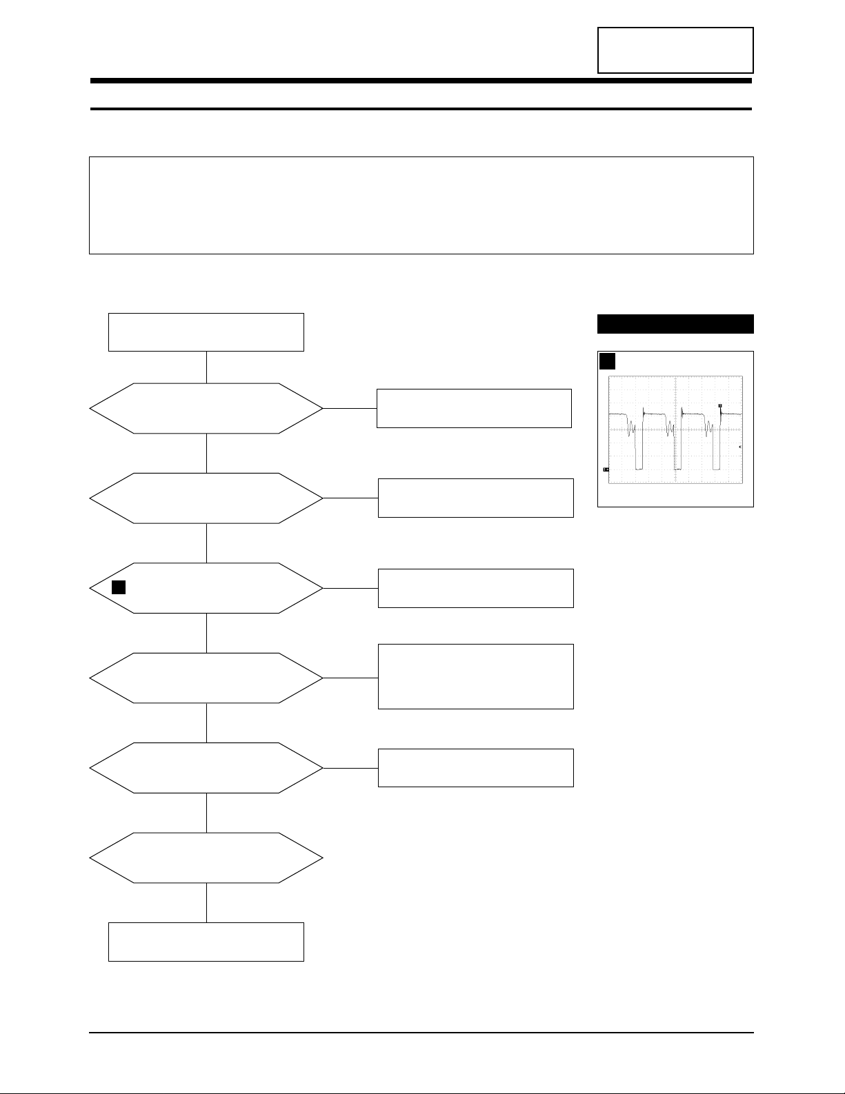
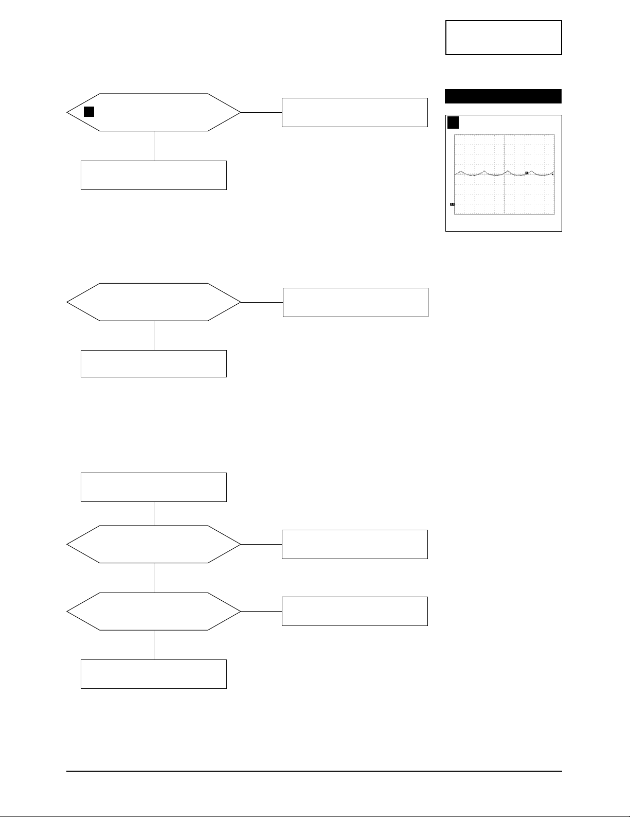
WAVEFORMS
1
1
100 V (IC601, #1)
CH1 P-P = 100 V CH1 RMS = 350.2 V
CONFIDENTIAL
5 Troubleshooting
5-2 AN17K*/AN17L*
5-1-2 DPMS Failure
Make No H/V Sync. (power off mode)
Check signal source
H/V Sync. video level.
LED blinks?
Check IC201 Pin 40.
Yes
No
+12 V line off?
Check IC201 Pin 5/Pin 6 and
Q610/Q602 operation.
Yes
No
Yes
Q602 Base voltage exists?
Check IC201 Pin 5.
Check and replace Q602 and IC201.
No
IC601 Pin 1 output
voltage exists?
Refer to 5-1-1 No Power Supply.
Done
Yes
No
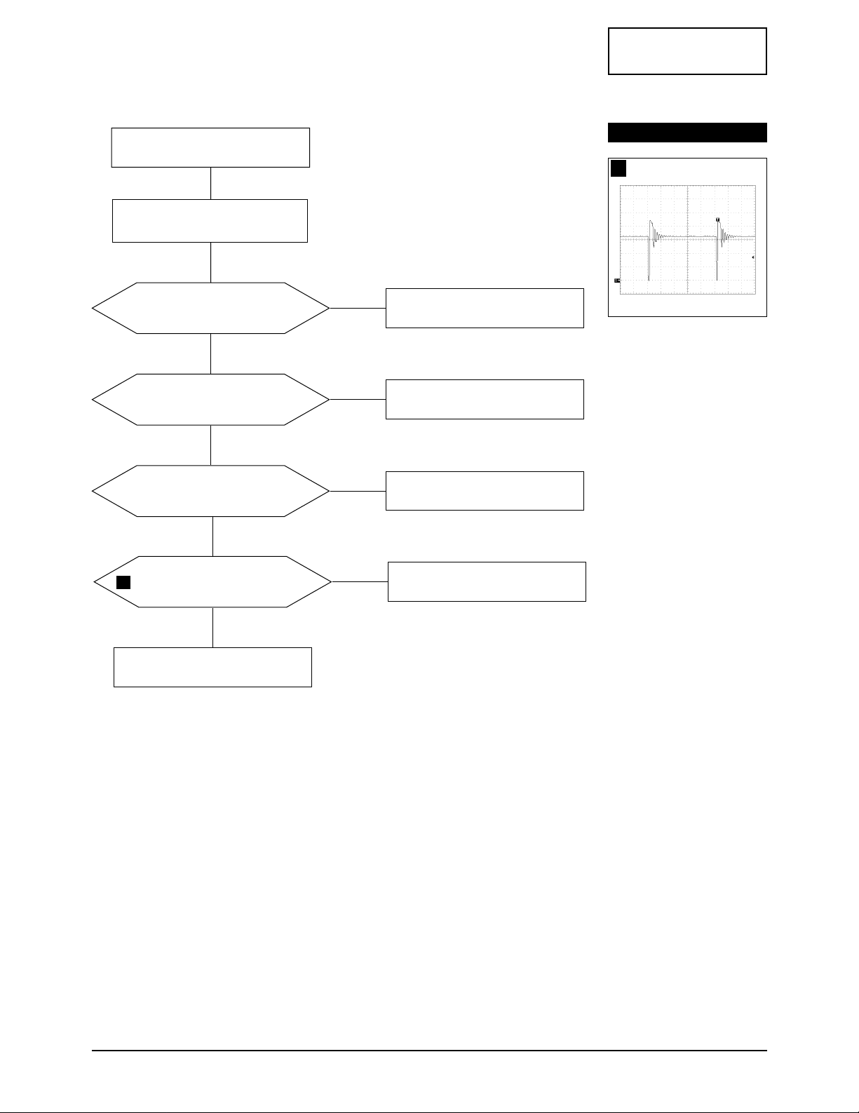
2
2
100V (IC601, #1)
CH1 P-P = 100V CH1 RMS = 325.8 V
WAVEFORMS
CONFIDENTIAL
5 Troubleshooting
AN17K*/AN17L* 5-3
5-1-3 H_Deflection Failure
Does Horizontal pluse signal
appear at Pin 26 of IC401?
Check IC401.
Yes
No
Does 110 Vp-p signal appear
at Collector of Q403?
Check Q403.
Yes
No
Check Q402, Q404 and T401.
4
Does PWM output signal appear
at Pin 28 (B_DRV) of IC401?
Check IC401.
Check 12 V line.
Yes
No
Does DC 12V appear at
Pin 29 of IC401?
Yes
No
3
5-1-4 S Correction Failure
S1~S3 signals are correct at each
frequency block?
Check S1 ~ S3 signal.
Check and replace Q409, Q410,
Q411, Q414, Q415, Q416, D402,
D403, QD404.
Yes
Check and replace IC201.
No
5
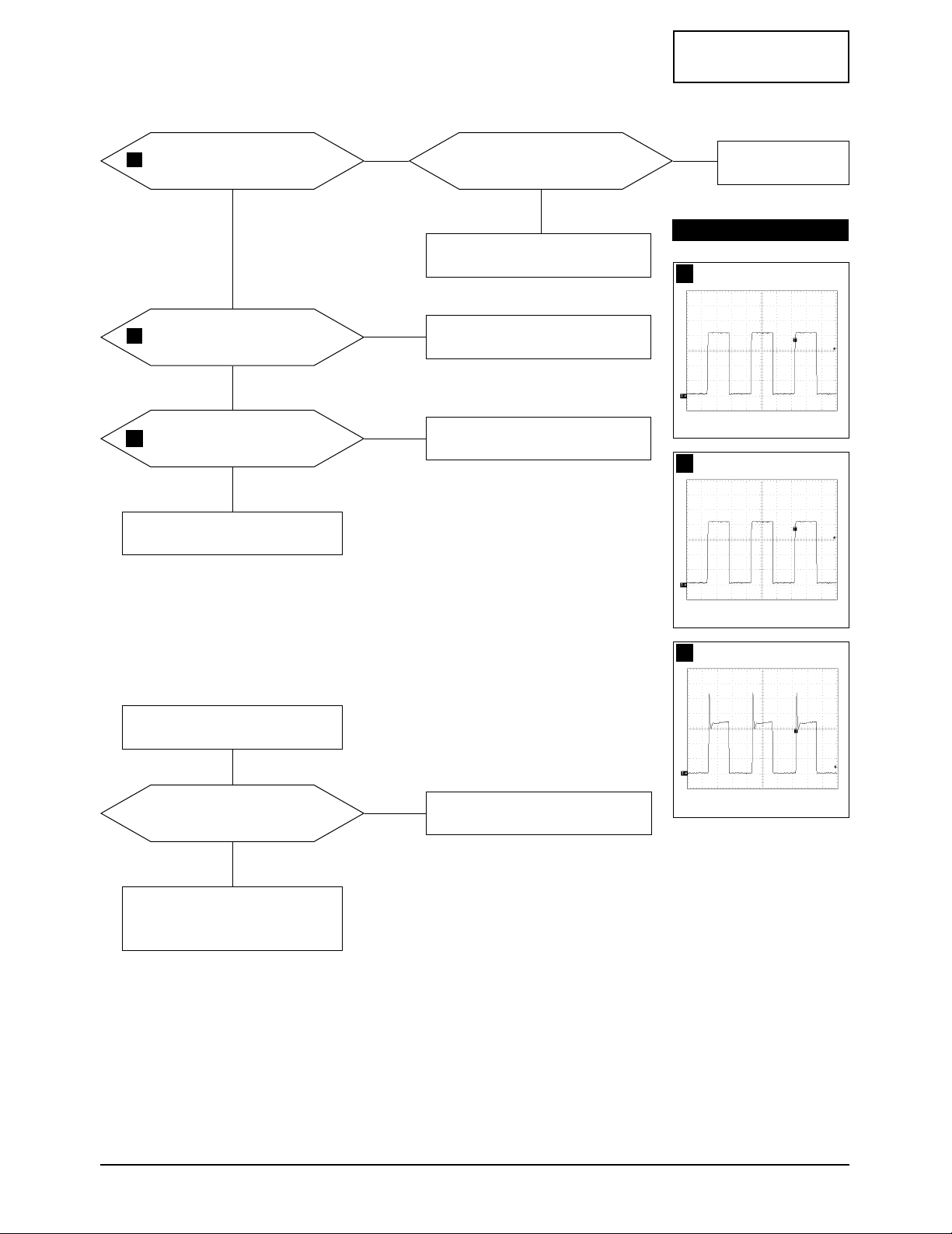
3
2.00 V (IC401, #28)
CH1 P-P = 2.00V CH1 RMS = 5.868V
4
2.00V (IC401, #26)
CH1 P-P = 2.00V CH1 RMS = 5.868V
5
20.0 V (Q403, Collector)
CH1 P-P = 20.0 V CH1 RMS = 46.80V
WAVEFORMS
CONFIDENTIAL
5 Troubleshooting
5-4 AN17K*/AN17L*
5-1-5 H_Lin. Failure Check and Replace T402
5-1-6 Invariable H_Size
IC401 Pin 28 voltage varies with
different B_DRV DAC values?
Q402 Gate output duty varies with
different B_DRV DAC values?
Check some parts around Q402,
IC401 Pin 14 ~ 16.
Yes
No
Check and replace IC401.
No
5-1-7 Abnormal H_Size
IC401 Pin 24 output duty
varies with different B+ offset
DAC values?
Q404 Collector
waveform is right?
Check and replace Q405,
Q406, Q407, and Q408.
Check Components
around D409 and L401.
Yes
Yes
No
Check and replace IC201.
No
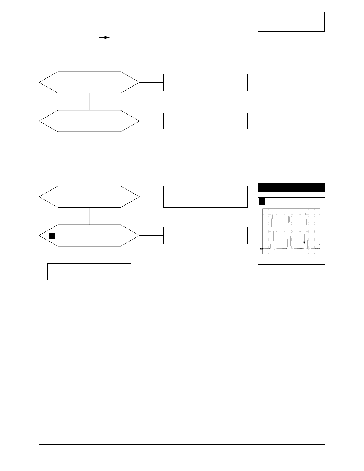
6
6
200 V (Q404, Collector)
CH1 P-P = 200V CH1 RMS = 387.2V
WAVEFORMS
CONFIDENTIAL
5 Troubleshooting
AN17K*/AN17L* 5-5
5-1-8 Side Pin or Trap Failure
IC401 Pin 24 output exists?
Yes
Check and replace IC401.
Refer to 5-1-7
Abnormal H_Size
.
5-1-9 Para. or Pin Balance Failure
IC401 Pin 24 output varies with
different DAC values?
No
Replace IC401.
No
7
5-1-10 Tilt Failure
IC201 Pin 20 output duty varies
with different DAC values?
Q611 Base output varies with
different DAC values?
Check and replace Q611.
Check and replace Q301 and Q302.
Yes
Yes
No
Check and replace IC201.
No
Check tilt connector connection
Refer to 5-1-7
Abnormal H_Size
.
Yes
7
1.00 V (IC401, #24)
CH1 P-P = 1.00V CH1 RMS = 3.008 V
WAVEFORMS
CONFIDENTIAL
5 Troubleshooting
5-6 AN17K*/AN17L*
5-1-11 V Deflection Failure
13V and –13V lines are on?
IC401 Pin 23 output exists?
Check and replace IC401.
Yes
Yes
No
Refer to 5-1-1 No Power Supply
No
IC301 Pin 6 output exists?
Check and replace
components around IC301.
Yes
No
Check DY connector connection.
8
9
5-1-12 V Size or Position Variation Failure
IC401 Pin 23 output varies with
different DAC values?
Yes
Check and replace IC201 and IC401.
Check and replace IC301.
No
8
500 V (IC401, #23)
CH1 P-P = 500 V CH1 RMS = 1.425 V
9
10.0 V (IC301, #6)
CH1 P-P = 10.0 V CH1 RMS = 5.06 V
WAVEFORMS
CONFIDENTIAL

5 Troubleshooting
AN17K*/AN17L* 5-7
5-1-13 High Voltage Failure
IC401 Pin 28 OSC pulse exists?
Q402 Gate driving pulse exists?
Check and replace Q401 and Q420.
Yes
Yes
No
Check and replace IC401
and +12 V line.
No
Q402 Drain pulse exists?
Check and replace
Q402, L402 and D401.
Check 50V Line.
Yes
No
Done
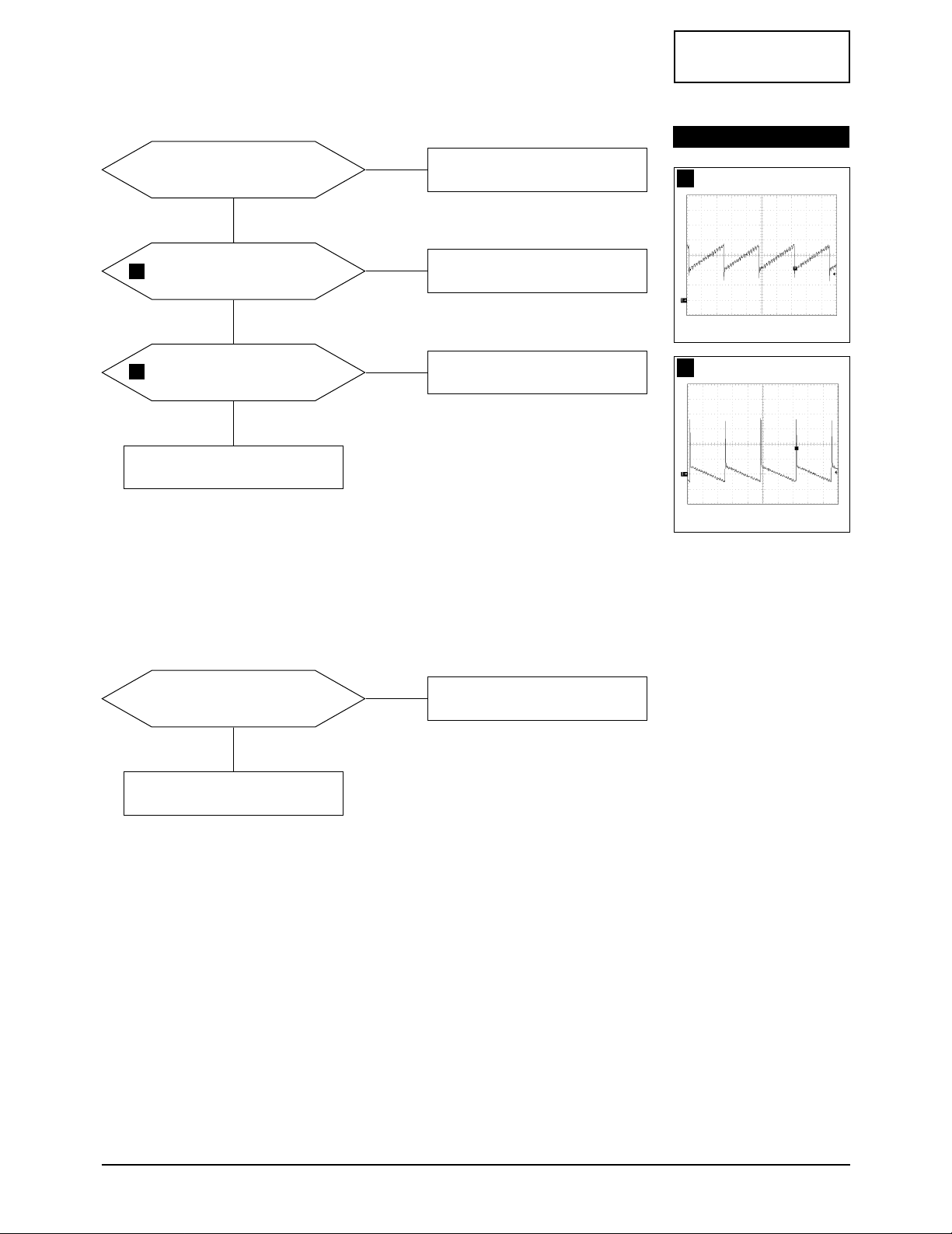
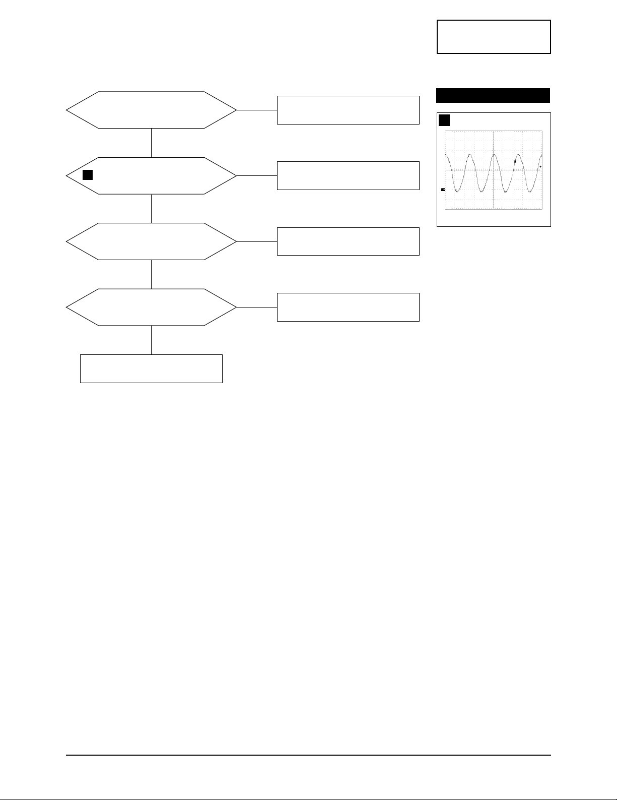
10
3
IC101 Pin 8 input exists and
varies with different patterns?
Check and replace IC101.
Input full white pattern to monitor.
Yes
No
T501 Pin 8 output exists?
Check and replace T501.
Yes
No
IC201 Pin 26 output exists and
varies with different patterns?
Check and replace IC201.
Yes
No
Done
Check CN102.
5-1-14 ABL Failure
11
3
2.00 V (IC401, #28)
CH1 P-P = 2.00 V CH1 RMS = 5.868 V
10
2.00 V (Q402, Gate)
CH1 P-P = 2.00 V CH1 RMS = 7.692V
11
50.0 V (Q402, Drain)
CH1 P-P = 50.0 V CH1 RMS = 73.7V
WAVEFORMS
CONFIDENTIAL

5 Troubleshooting
5-8 AN17K*/AN17L*
5-1-15 Dynamic Focus Failure
IC401 Pin 32 output is right?
Some parts around Q551 are right?
Replace failed part.
Yes
Yes
No
Replace the IC401.
No
T502 Pin 6 input is right?
Check and replace C432.
Yes
No
T502 Pin 1 output is right?
Replace the T502.
Yes
No
Check the connection between FBT
Focus pin and CRT Socket PCB.
13
14
12
12
2.00 V (IC401, #32)
CH1 P-P = 2.00V CH1 RMS = 6.124V
13
50.0 V (T502, #6)
CH1 P-P = 50.0V CH1 RMS = 75.6V
14
100 V (T502, #1)
CH1 P-P = 100V CH1 RMS = 124.0V
WAVEFORMS
CONFIDENTIAL

5 Troubleshooting
AN17K*/AN17L* 5-9
5-1-16 No Video
IC101 Pin 12, 14 and 16 inputs
are right?
IC101 Pin 18, 21 and 24
outputs are right?
Check I2C bus and +12V line.
Yes
Yes
No
Check the signal cable connection.
No
IC102 Pin 9, 10 and 11
outputs are right?
Check +12V, +80V line.
Check and replace IC102.
Yes
No
Cathode DC levels are right?
Check +80V line.
Check and replace IC104.
Yes
No
G2 voltage is right?
Check G2 wire, CRT Socket board
and FBT.
Change CRT.
Yes
Done.
No
Check signal cable and connection.
15
16
17
15
1.00V (IC101 #12,14,16)
CH1 P-P = 1.00V CH1 RMS = 2.452V
16
1.00V (IC101 #18,21,24)
CH1 P-P = 1.00V CH1 RMS = 2.792V
17
20.0V (IC102, #9, 10, 11)
CH1 P-P = 20.0V CH1 RMS = 40.52V
WAVEFORMS
CONFIDENTIAL
5 Troubleshooting
5-10 AN17K*/AN17L*
5-1-17 Micom Failure
IC201 Pin 11 input voltage is 5V?
IC201 Pin 13 and 14 inputs
are right?
Check C202, C203 and X201.
Yes
Yes
No
Check IC604.
No
IC201 Pin 18 input is right?
Check and replace IC201 and R206.
Yes
No
All in/output values are right?
Replace IC201.
Yes
No
Done
18
18
1.00 V (IC201, #13, 14)
CH1 P-P = 1.00 V CH1 RMS = 2.108V
WAVEFORMS
CONFIDENTIAL

5 Troubleshooting
AN17K*/AN17L* 5-11
5-1-18 OSD Failure
IC101 Pin 32 input is right?
IC101 Pin 1 input is right?
Check CN102 Pin 8.
Yes
Yes
No
Check and replace
R117, C117 and IC101.
No
IC101 Pin 29 and 30 inputs are
right?
Check IC201 Pin 41 and 42.
Yes
No
Check and replace IC102.
Yes
Done
19
20
Check CN102 and connector Ass’y.
Yes
IC101 Pin 18, 21 and 24
outputs are right?
Check and replace IC101.
No
21
19
1.00 V (IC101, #32)
CH1 P-P = 1.00V CH1 RMS = 4.516V
20
1.00 V (IC101, #1)
CH1 P-P = 1.00V CH1 RMS = 5.024V
21
1.00 V (IC101, #18,21,24)
CH1 P-P = 1.00V CH1 RMS = 2.580V
WAVEFORMS
CONFIDENTIAL
5 Troubleshooting
5-12 AN17K*/AN17L*
5-1-19 User Control Failure
Does the DC level change at
Pin 38 of IC201 when you
push the S/W button?
Yes
Check the button.
(SW201 ~ SW204)
No
Check IC201.
RL601 operation is right?
Q601 base input is right?
Check and replace Q601.
No
No
Yes
Check D-coil and TH601.
Yes
IC201 Pin 4 output is right?
Check and replace IC201.
Yes
No
Done
Check degaussing connector.
5-1-20 Degaussing Failure
CONFIDENTIAL

5 Troubleshooting
AN17K*/AN17L* 5-13
5-2 General Troubleshooting
5-2-1 No Picture
LED blinks?
LED is green color?
Check Micom.
Check G2 voltage, high voltage
and R, G, B cathode voltage.
No
No
Yes
Refer to 5-2-2 Shut down.
Yes
5-2-2 Shut Down
Blinking LED’s?
Scan failure?
Check horizontal, vertical deflection
system and check power supply
secondary voltages.
Yes
Yes
Check power supply.
No
Check and replace IC201.
Done
No
Video failure?
Check Video board.
No
Yes
CONFIDENTIAL

5 Troubleshooting
5-14 AN17K*/AN17L*
5-2-3 Missing Color
Proper Video levels are
on CN101 (D-Sub) Pin 1, 3 and 5?
Proper Video signal
to all cathodes?
Refer to 5-1-16 No Video.
Yes
Yes
No
Check signal generator.
No
Proper DC voltage to all cathodes?
Check IC101 Pin 17, 20 and 23.
Check IC104.
Yes
Yes
No
G2 voltage is right?
Check T501 and D502, D512.
No
Heater voltage is right?
Check D608, Q604 and T601.
No
Yes
Check D504, Q502 and T501.
No
Yes
Yes
G1 voltage is right?
No
Replace CRT.
Done
22
22
10.0 V (R,G,B, Video)
CH1 P-P = 10.0V CH1 RMS = 17.02V
WAVEFORMS
CONFIDENTIAL

5 Troubleshooting
AN17K*/AN17L* 5-15
G2 voltage is right?
Blank pulse at Pin 3 of IC401?
Check IC401.
Yes
Yes
No
Check D502, D512.
No
V_FLB pulse at
Collector of Q303?
Check Q303.
Done
Yes
No
Valid the Vertical pulse
on CRT Socket G1?
Check CN102 and CN201.
Yes
No
Check white balance adjustment.
5-2-4 Visible Retrace
23
24
23
5.00V (Q303, Collector)
CH1 P-P = 5.00V CH1 RMS = 28.33V
24
20.00V (CRT Socket, G1)
CH1 P-P = 20.0V CH1 RMS = 66.68V
WAVEFORMS
CONFIDENTIAL

5 Troubleshooting
5-16 AN17K*/AN17L*
Signals are right?
Signals at Pin 28 and 29 of
IC201 are right?
Check IC201.
Yes
Yes
No
Check Video Cable
No
Signals at Pin 1 and 2 of
IC401 are right?
Check IC401
Check circuits on Main board.
Yes
Done
No
Check input signals Pin 2
and 3 of CN202.
5-2-5 Unsynchronized Image
CONFIDENTIAL

5 Troubleshooting
AN17K*/AN17L* 5-17
Convergence is now
within spec.?
Readjust convergence.
No
Done
Yes
Convergence is now
within spec.?
Done
Change CRT and readjust
convergence.
No
Done
Yes
Adjust convergence.
5-2-6 Misconvergence
CONFIDENTIAL

5 Troubleshooting
5-18 AN17K*/AN17L*
Improved focus?
Check focus leads from FBT
to CRT Socket.
Check CRT Socket.
No
Align monitor and
check for focus change.
Yes
Dynamic focus circuit is right?
Refer to 5-1-15 Dynamic
Focus Failure.
Replace the CRT and verify focus.
Yes
No
Adjust focus VR of FBT.
5-2-7 Poor Focus
5-2-8 Purity Failure
Purity is correct?
Degaussing circuit is correct?
Refer to 5-1-20 Degaussing Failure.
Replace CRT and verify purity.
Yes
No
No
Done
Yes
Degause
CONFIDENTIAL
 Loading...