

Samsung 1080-P-7 Service manual
DVD PLAYER
Chassis: BRINO Hyper
BASIC :
DVD-1080P7
Application Model
: DVD-1080P7
Application Areas
: AUS, CHN, EUR, NWT, XEC, XEE,
XEF, XEG, XEH, XEL, XEO, XER, XET,
XEU, XFA, XSA, XSE, XSG, XSH, XSS,
XST
SERVICE
Π45mm With LED
´ Zoran Vaddis 966 1Chip Solution
ˇ DivX Playback Support
¨ Multi Proggressive Scan
ˆ HDMI - Anynet
Ø 14Bit Video DAC
Manual
DVD PLAYER
Merit & Character regarding Product
SERVICE MANUAL
DVD-1080P7
OPEN/CLOSE
© Samsung Electronics Co., Ltd. MAY . 2007
Printed in Korea
AK82-01232A
This Service Manual is a property of Samsung Electronics Co.,Ltd.
Any unauthorized use of Manual can be punished under applicable
international and/or domestic law.
Area Web Site
North America URL ; http://service.samsungportal.com
Latin America URL ; http://latin.samsungportal.com
CIS URL ; http://cis.samsungportal.com
Europe URL ; http://europe.samsungportal.com
China URL ; http://china.samsungportal.com
Asia URL ; http://asia.samsungportal.com
Mideast & Africa URL ; http://mea.samsungportal.com
If you want to know additional information which is not included on this
Service Manual, Please refer to the SKP(Samsung Knowledge Portal)
web site.
ELECTRONICS

CONTENTS
1. Precautions 1-1 ~ 1-6
1-1 Safety Precautions (1-1)
1-2 Servicing Precautions (1-3)
1-3 ESD Precautions (1-4)
1-4 Handling the optical pick-up (1-5)
1-5 Pick-up disassembly and reassembly (1-6)
2. Product Specification 2-1 ~ 2-4
2-1 Product Specification (2-1)
2-2 Chassis Product Specification (2-2)
2-3 Option Product Specification (2-3)
3. Alignment and Adjustment 3-1 ~ 3-4
3-1 Location of Test Point (3-1)
3-2 Skew Adjustment (3-2)
4. Disassembly and Reassembly 4-1 ~ 4-10
4-1 Cabinet and PCB (4-1)
4-2 Deck (4-5)
5. Trouble Shooting 5-1 ~ 5-14
6. Exploded View and Parts List 6-1 ~ 6-6
6-1 Cabinet Assembly (6-2)
6-2 DVD Mechanical Parts (6-4)
7. Electrical Parts List 7-1 ~ 7-6
8. Block Diagrams 8-1 ~ 8-6
8-1 All Block Diagram (8-2)
8-2 ZIC1 (Vadiss 966 Integration) Block Diagram (8-3)
8-3 ZIC2 (SDRAM) Block Diagram (8-4)
8-4 MIC1 (AM5766) Block Diagram (8-5)
9. Wiring Diagram 9-1 ~ 9-2

CONTENTS
10. PCB Diagrams 10-1 ~ 10-8
10-1 DVD Main PCB (10-2)
10-2 SMPS PCB (10-4)
10-3 Front Key PCB (10-6)
10-4 Power Key PCB (10-7)
11. Schematic Diagrams 11-1 ~ 11-14
11-1 S.M.P.S (S.M.P.S PCB) (11-2)
11-2 Audio (Main PCB) (11-3)
11-3 AV Decoder (Main PCB) (11-4)
11-4 Servo (Main PCB) (11-5)
11-5 Video (Main PCB) (11-6)
11-6 Connector (Main PCB) (11-7)
11-7 HDMI (Main PCB) (11-8)
11-8 CEC (Main PCB) (11-9)
11-9 Front MCU LED Modul (Front Key PCB) (11-10)
11-10 Key (Power Key PCB) (11-11)
12. Operating Instructions 12-1 ~ 12-10
13. Circuit Operating Descriptions 13-1 ~ 13-16
13-1 Power (13-1)
13-2 RF (13-7)
13-3 System Control (13-8)
13-4 Servo (13-9)
13-5 DVD Data Processor (13-12)
13-6 Video (13-13)
13-7 Audio (13-14)
14. Reference Information 14-1 ~ 14-18
14-1 Introduction to DVD (14-1)
14-2 DVD-Video Format (14-3)
14-3 About HDMI (14-9)
14-4 DivX (14-13)
14-5 Setting Up The Anynet + HDMI-CEC (14-16)
14-6 Firmware Upgrade (14-18)
Samsung Electronics 1-1
1. Precautions
1-1 Safety Precautions
1) Before returning an instrument to the customer,
always make a safety check of the entire instrument,
including, but not limited to, the following items:
(1) Be sure that no built-in protective devices are
defective or have been defeated during servicing.
(1)Protective shields are provided to protect both
the technician and the customer. Correctly replace
all missing protective shields, including any
removed for servicing convenience.
(2)When reinstalling the chassis and/or other assembly in the cabinet, be sure to put back in place
all protective devices, including, but not limited to,
nonmetallic control knobs, insulating fish papers,
adjustment and compartment covers/shields, and
isolation resistor/capacitor networks. Do not operate this instrument or permit it to be operated without all protective devices correctly installed and
functioning.
(2) Be sure that there are no cabinet openings through
which adults or children might be able to insert
their fingers and contact a hazardous voltage. Such
openings include, but are not limited to, excessively wide cabinet ventilation slots, and an improperly fitted and/or incorrectly secured cabinet back
cover.
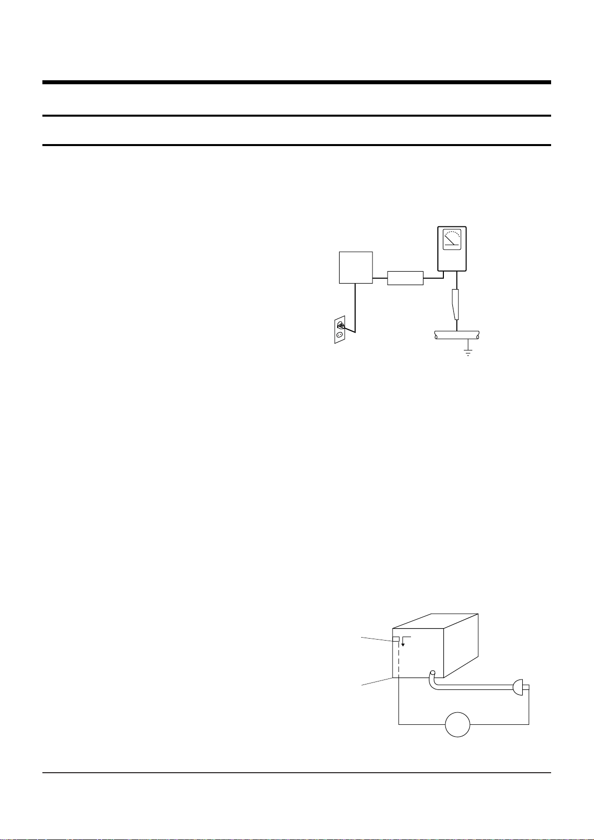
(3) Leakage Current Hot Check-With the instrument
completely reassembled, plug the AC line cord
directly into a 120V AC outlet. (Do not use an isolation transformer during this test.) Use a leakage
current tester or a metering system that complies
with American National Standards institute (ANSI)
C101.1 Leakage Current for Appliances and
Underwriters Laboratories (UL) 1270 (40.7). With
the instrument’s AC switch first in the ON position
and then in the OFF position, measure from a
known earth ground (metal water pipe, conduit,
etc.) to all exposed metal parts of the instrument
(antennas, handle brackets, metal cabinets, screwheads, metallic overlays, control shafts, etc.), especially any exposed metal parts that offer an electrical return path to the chassis.
Any current measured must not exceed 0.5mA.
Reverse the instrument power cord plug in the outlet and repeat the test. See Fig. 1-1.
Any measurements not within the limits specified
herein indicate a potential shock hazard that must
be eliminated before returning the instrument to
the customer.
Fig. 1-1 AC Leakage Test
(4) Insulation Resistance Test Cold Check-(1) Unplug
the power supply cord and connect a jumper wire
between the two prongs of the plug. (2) Measure
the resistance with an ohmmeter between the
jumpered AC plug and all exposed metallic cabinet
parts on the instrument, such as screwheads,
antenna, control shafts, handle brackets, etc. When
an exposed metallic part has a return path to the
chassis, the reading should be between 1 and 5.2
megohm. When there is no return path to the chassis, the reading must be infinite. If the reading is
not within the limits specified, there is the possibility of a shock hazard, and the instrument must be
repaired and rechecked before it is returned to the
customer. See Fig. 1-2.
Fig. 1-2 Insulation Resistance Test
(READING SHOULD
NOT BE ABOVE
0.5mA)
EARTH
GROUND
DEVICE
UNDER
TEST
TEST ALL
EXPOSED METER
SURFACES
2-WIRE CORD
ALSO TEST WITH
PLUG REVERSED
(USING AC ADAPTER
PLUG AS REQUIRED)
LEAKAGE
CURRENT
TESTER
Antenna
Terminal
Exposed
Metal Part
ohm
ohmmeter

Precautions
1-2 Samsung Electronics
2) Read and comply with all caution and safety related notes on or inside the cabinet, or on the chassis.
3) Design Alteration Warning-Do not alter or add to
the mechanical or electrical design of this instrument. Design alterations and additions, including
but not limited to, circuit modifications and the
addition of items such as auxiliary audio output
connections, might alter the safety characteristics of
this instrument and create a hazard to the user. Any
design alterations or additions will make you, the
servicer, responsible for personal injury or property
damage resulting therefrom.
4) Observe original lead dress. Take extra care to
assure correct lead dress in the following areas:
(1) near sharp edges, (2) near thermally hot parts (be
sure that leads and components do not touch thermally hot parts), (3) the AC supply, (4) high voltage,
and (5) antenna wiring. Always inspect in all areas
for pinched, out-of-place, or frayed wiring, Do not
change spacing between a component and the
printed-circuit board. Check the AC power cord for
damage.
5) Components, parts, and/or wiring that appear to
have overheated or that are otherwise damaged
should be replaced with components, parts and/ or
wiring that meet original specifications.
Additionally, determine the cause of overheating
and/or damage and, if necessary, take corrective
action to remove any potential safety hazard.
6) Product Safety Notice-Some electrical and mechanical parts have special safety-related characteristics
which are often not evident from visual inspection,
nor can the protection they give necessarily be
obtained by replacing them with components rated
for higher voltage, wattage, etc. Parts that have special safety characteristics are identified by shading,
an ( )or a ( )on schematics and parts lists. Use
of a substitute replacement that does not have the
same safety characteristics as the recommended
replacement part might create shock, fire and/or
other hazards. Product safety is under review continuously and new instructions are issued whenever appropriate.

Precautions
Samsung Electronics 1-3
1-2 Servicing Precautions
CAUTION : Before servicing units covered by this
service manual and its supplements, read and follow
the Safety Precautions section of this manual.
Note : If unforseen circumstances create conflict
between the following servicing precautions and any
of the safety precautions, always follow the safety precautions. Remember: Safety First.
1-2-1 General Servicing Precautions
(1) a. Always unplug the instrument’s AC power cord
from the AC power source before (1) removing
or reinstalling any component, circuit board,
module or any other instrument assembly, (2)
disconnecting any instrument electrical plug or
other electrical connection, (3) connecting a test
substitute in parallel with an electrolytic capacitor in the instrument.
b. Do not defeat any plug/socket B+ voltage inter-
locks with which instruments covered by this
service manual might be equipped.
c. Do not apply AC power to this instrument and
/or any of its electrical assemblies unless all
solid-state device heat sinks are correctly installed.
d. Always connect a test instrument’s ground lead
to the instrument chassis ground before connecting the test instrument positive lead. Always
remove the test instrument ground lead last.
Note : Refer to the Safety Precautions section ground
lead last.
(2) The service precautions are indicated or printed on
the cabinet, chassis or components. When servicing, follow the printed or indicated service precautions and service materials.
(3) The components used in the unit have a specified
flame resistance and dielectric strength.
When replacing components, use components
which have the same ratings. Components identified by shading, by( ) or by ( ) in the circuit diagram are important for safety or for the characteristics of the unit. Always replace them with the exact
replacement components.
(4) An insulation tube or tape is sometimes used and
some components are raised above the printed
wiring board for safety. The internal wiring is
sometimes clamped to prevent contact with heating components. Install such elements as they
were.
(5) After servicing, always check that the removed
screws, components, and wiring have been installed correctly and that the portion around the
serviced part has not been damaged and so on.
Further, check the insulation between the blades of
the attachment plug and accessible conductive
parts.
1-2-2 Insulation Checking Procedure
Connect the insulation resi-stance meter (500V) to the
blades of the attachment plug. The insulation resistance between each blade of the attachment plug and
accessible conductive parts(see note) should be more
than 1 Megohm.
Note : Accessible conductive parts include metal panels, input terminals, earphone jacks, etc.

Precautions
1-4 Samsung Electronics
1-3 ESD Precautions
Electrostatically Sensitive Devices (ESD)
Some semiconductor (solid state) devices can be damaged easily by static electricity.
Such components commonly are called Electrostatically Sensitive Devices(ESD). Examples of typical ESD
devices are integrated circuits and some field-effect
transistors and semiconductor chip components. The
following techniques should be used to help reduce
the incidence of component damage caused by static
electricity.
(1) Immediately before handling any semiconductor
component or semiconductor-equipped assembly,
drain off any electrostatic charge on your body by
touching a known earth ground. Alternatively,
obtain and wear a commercially available discharging wrist strap device, which should be
removed for potential shock reasons prior to applying power to the unit under test.
(2) After removing an electrical assembly equipped
with ESD devices, place the assembly on a conductive surface such as aluminum foil, to prevent electrostatic charge buildup or exposure of the assembly.
(3) Use only a grounded-tip soldering iron to solder or
unsolder ESD devices.
(4) Use only an anti-static solder removal devices.
Some solder removal devices not classified as
“anti-static” can generate electrical charges sufficient to damage ESD devices.
(5) Do not use freon-propelled chemicals. These can
generate electrical charges sufficient to damage
ESD devices.
(6) Do not remove a replacement ESD device from its
protective package until immediately before your
are ready to install it.(Most replacement ESD
devices are packaged with leads electrically shorted together by conductive foam, aluminum foil or
comparable conductive materials).
(7) Immediately before removing the protective ma-
terials from the leads of a replacement ESD device,
touch the protective material to the chassis or circuit assembly into which the device will be
installed.
CAUTION : Be sure no power is applied to the chassis or circuit, and observe all other safety precautions.
(8) Minimize bodily motions when handling unpack-
aged replacement ESD devices. (Otherwise harmless motion such as the brushing together of your
clothes fabric or the lifting of your foot from a carpeted floor can generate static electricity sufficient
to damage an ESD device).

Precautions
Samsung Electronics 1-5
1-4 Handling the optical pick-up
The laser diode in the optical pick up may suffer electrostatic breakdown because of potential static electricity from clothing and your body.
The following method is recommended.
(1) Place a conductive sheet on the work bench (The
black sheet used for wrapping repair parts.)
(2) Place the set on the conductive sheet so that the
chassis is grounded to the sheet.
(3) Place your hands on the conductive sheet(This
gives them the same ground as the sheet.)
(4) Remove the optical pick up block
(5) Perform work on top of the conductive sheet. Be
careful not to let your clothes or any other static
sources to touch the unit.
◆ Be sure to put on a wrist strap grounded to the
sheet.
◆ Be sure to lay a conductive sheet made of copper
etc. Which is grounded to the table.
Fig.1-3
(6) Short the short terminal on the PCB, which is in-
side the Pick-Up ASS’Y, before replacing the PickUp. (The short terminal is shorted when the PickUp Ass’y is being lifted or moved.)
(7) After replacing the Pick-up, open the short termi-
nal on the PCB.
WRIST-STRAP
FOR GROUNDING
1M
THE UNIT
1M
CONDUCTIVE SHEET
Precautions
1-6 Samsung Electronics
1-5 Pick-up disassembly and reassembly
1-5-1 Disassembly
1) Remove the power cord.
2) Disassemble the Deck-Assy, Please see Chapter 4
( Fig 4-22 ~ 4-26).
3) Make solder land 2 points short on Pick-up.
(See Fig. 1-4)
4) Disassemble the Pick-up, Please see Chapter 4
(Fig 4-22 ~ 4-26)
1-5-2 Assembly
1) Replace the Pick-up.
2) Remove the soldering 2 points on Pick-up.
3) Reassemble the Deck-Assy.
Note : If the assembly and disassembly are not done in correct sequence, the Pick-up may be damaged.
Fig. 1-4
PICK-UP ASS'Y
SOLDER LAND 2 POINTS SHORT
Power Requirements AC 120V ~ 60 Hz
Power Consumption 9W
Weight 1.042 lbs 0.065 oz
Dimensions 430mm(W) x 205mm(D) x 45mm (H)
Operating Temperature Range +5° F to +35° F
Operating Humidity Range 10% to 75%
DVD
Reading Speed : 3.49 ~ 4.06m/sec.
(Digital Versatile Disc)
Approx. Play Time
(Single Sided, Single Layer Disc) : 135min.
CD : 12Cm Reading Speed : 4.8 ~ 5.6m/sec.
(Compact Disc) Maximum Play Time : 74min.
CD : 8cm Reading Speed : 4.8 ~ 5.6m/sec.
(Compact Disc) Maximum Play Time : 20min.
Composite Video 1 channel : 1.0 Vp-p (75 Ω load)
Component Video Y: 1.0 Vp-p (75 Ω load)
Pr : 0.70 Vp-p (75 Ω load)
Pb: 0.70 Vp-p (75 Ω load)
S-Video
Luminance Signal : 1.0Vp-p (75 Ω load)
Chrominance Signal : 0.3Vp-p (75 Ω load)
HDMI 480p, 720p, 1080i
Scart Jack 2 Channel : L (1/L), R (2/R)
2 Channel L(1/L), R(2/R)
*Ferquency Response
48KHz Sampling : 4Hz to 22KHz
96KHz Sampling : 4Hz to 44KHz
*S/N Ratio 110dB
*Dynamic Range 100dB
*Total Harmonic Distortion 0.004%
Samsung Electronics
2-1
2. Product Specification
2-1 Product Specification
General
Disc
Audio Output
Video Output
Product Specification
2-2
Samsung Electronics
2-2 Chassis Product Specification
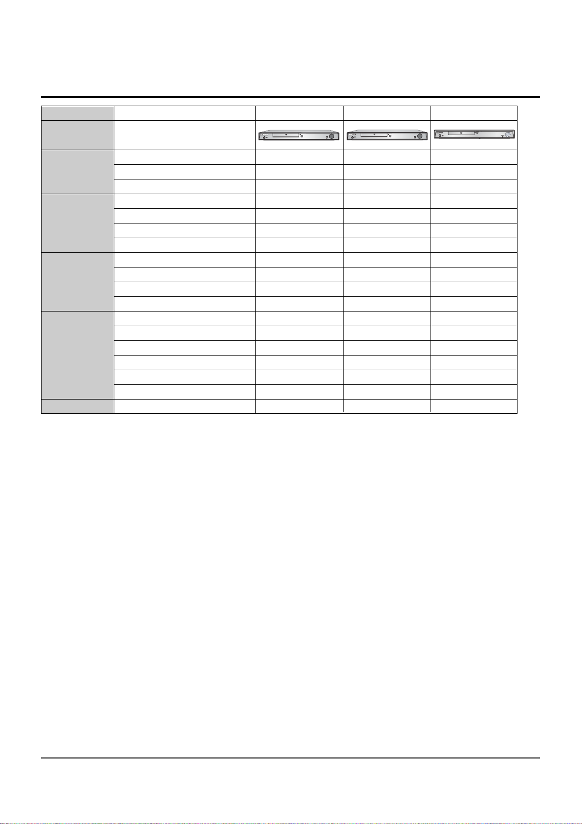
Classification Item DVD-1080P7/XAA DVD-1080P7/XSA DVD-HD870/XAA
DVD, CD, VCD, SVCD Disc Play O O O
DVD-R/-RW/+R/+RW(Video Mode) O O O
CD-R/-RW O O O
Progressive Scan Video O O O
108MHz/14 Bit Video DAC O O O
NTSC O O O
System Default NTSC PAL NTSC
MP3 / WMA Decoder O O O
MIC INPUT O X X
Digital Out (dts / AC-3) O O O
Audio DAC Built-in Built-in Built-in
VCD ,SVCD Playback O O O
DivX(MPEG 4) O O N
Instant Replay / Skip O O O
Kodak Picture CD(JPEG) / HD-JPEG O/X O/X O/O
FRONT DISPLAY LED LED LED
AUDIO VIDEO DIGITAL INTERFACE HDMI HDMI HDMI
HDMI Cable / HDMI to DVI Cable X/X X/X O/O
Compatibility
Video
Audio
ConvenienceAudio
Accessary
OPEN/CLOSE
OPEN/CLOSE
Product Specification
2-3
Samsung Electronics
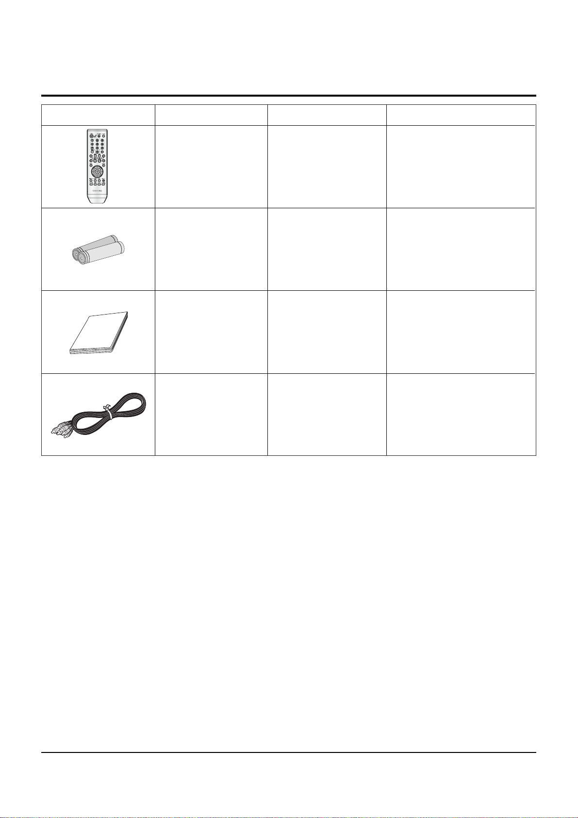
2-3 Option Product Specification
Description Fig Description Parts No Remark
Remote
Control
Batteries for
Remote Control
AK59-00061H
AC43-12002H
AK68-01397D
AC39-42001R
Owners Instructions
Video/Audio
Cable
Model Standard of
DVD-1080P7/XSA
Model Standard of
DVD-1080P7/XSA
Model Standard of
DVD-1080P7/XSA
Model Standard of
DVD-1080P7/XSA
S.N.A

Product Specification
2-4
Samsung Electronics
MEMO
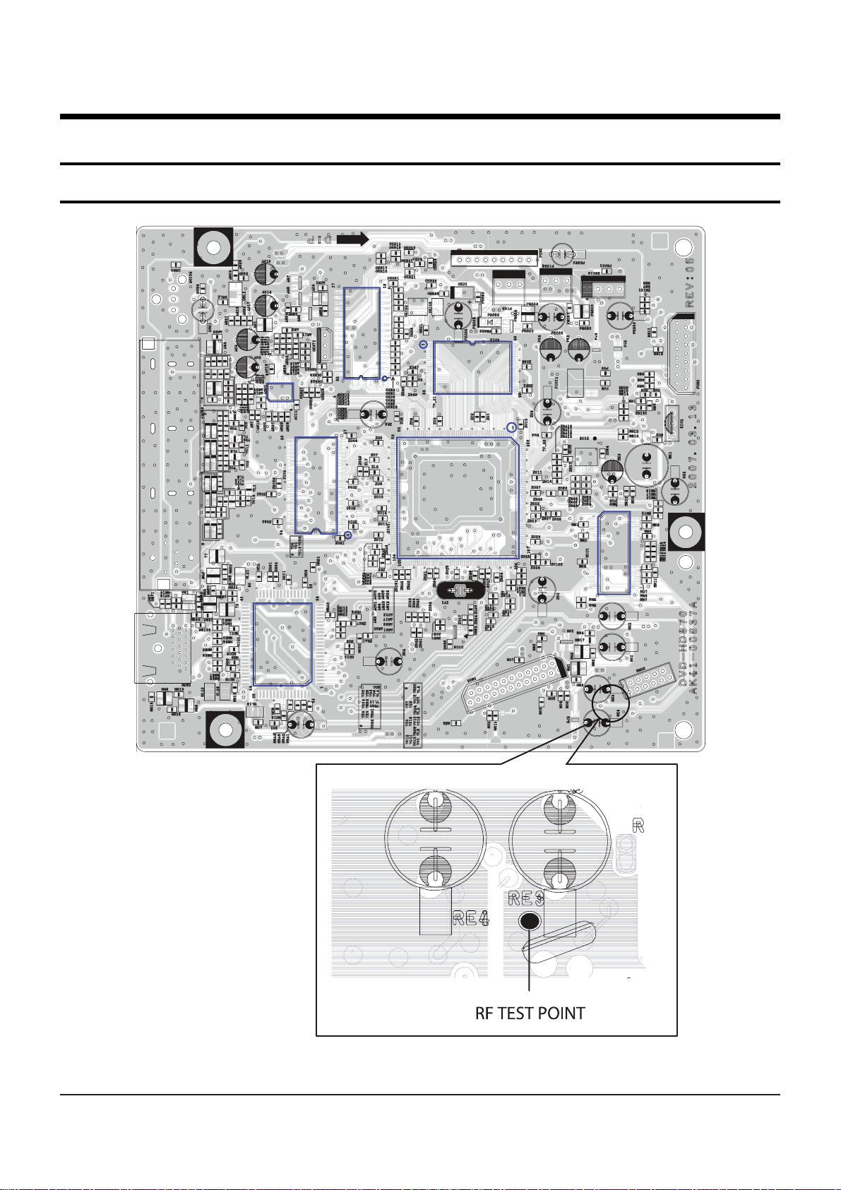
Samsung Electronics 3-1
3. Alignment and Adjustment
3-1 Location of Test Point
Fig. 3-1 Location of Test Point
AOP1
CE1C1
ZIC3
HIC1
ZIC2
ZIC1
MIC1

Alignment and Adjustment
3-2 Samsung Electronics
3-2-1 Adjustment Spec. and Test Point
3-2 Skew Adjustment
Test Disc Adjustment Spec. Test Point Adjustment Location
TDV-533 “RF Test Point” Screw A / B
Chapter 14 Flat Waveform (Main PCB - Component Side) Ass’y Deck - Top Side
(See Fig. 3-1) (See Fig. 3-2)
Fig. 3-2 Ass’y Deck (Top Side)
◆ Test Disc ; Service not Available
<Table 3-1>
Alignment and Adjustment
Samsung Electronics 3-3
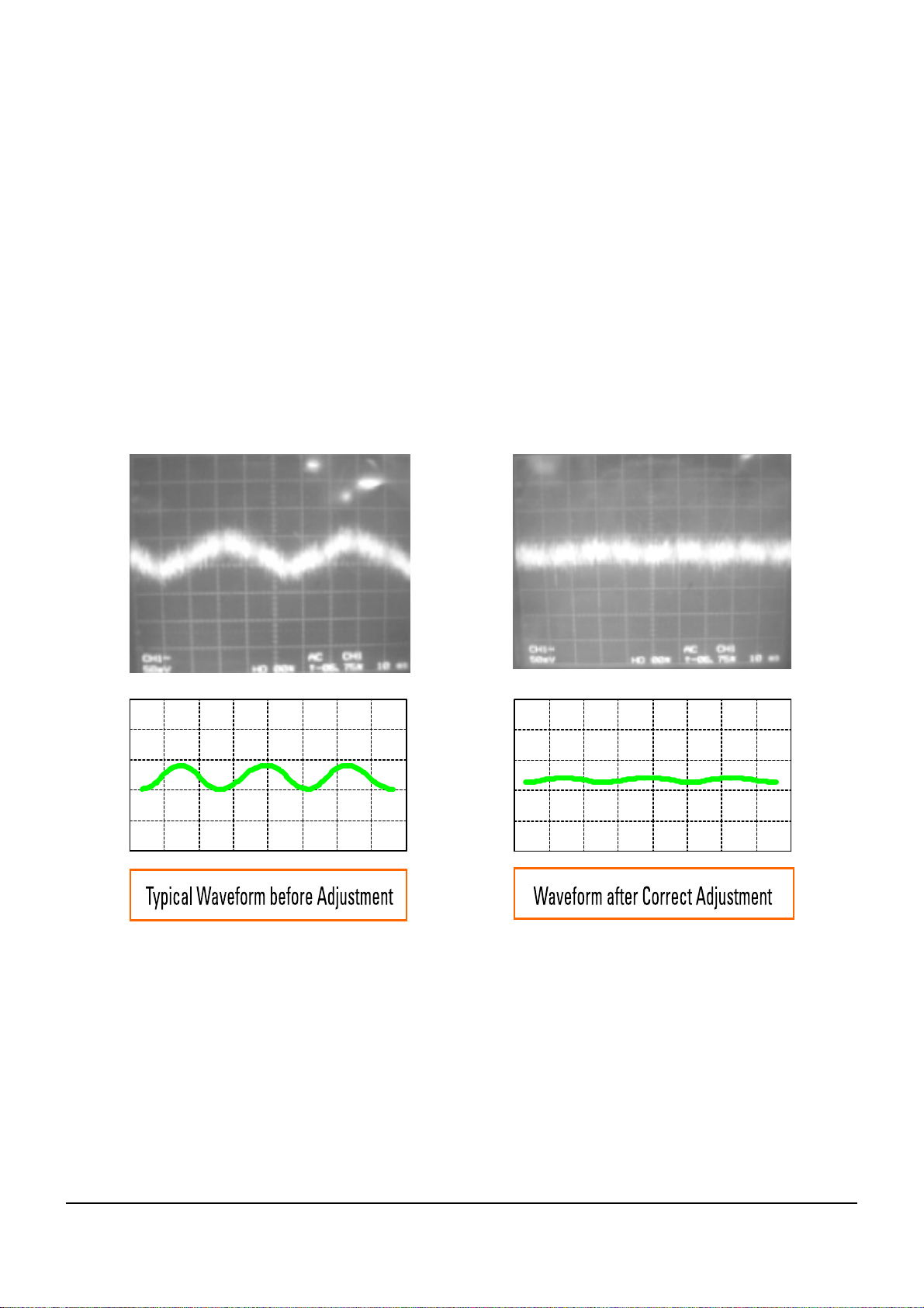
3-2-2 SKEW Adjustment Method
Needed to minimize the variations in Skew of the Pickup unit and to provide optimum match with the recorded
signal on the Disc.
1) Connect an Oscilloscope to the “RF Test Point ”(See Fig.3-1).
2) Connect Power, Open the Tray and Play “Ch.14 whish” is in the TDV-533 Disc.
◆ Set the Oscilloscope Range as follows :
(Voltage ;50mV/Div.,Frequency ;10m Sec.)
3) Adjust the Screws “A” and “B” (See Fig. 3-2) using a Hex screwdriver until you obtain a Flat Waveform and
the picture is stable.
Then, go to Chapter 1 and make sure the Waveform is Flat here as well.
If not, you have to go back to Chapter 14 and adjust again.
If you cannot obtain a Flat waveform, then the unit is defective.
Note : The Deck must be in a horizontal position. Use both “A” and “B” screws to adjust.
Fig.3-3 Envelope Waveform

Alignment and Adjustment
3-4 Samsung Electronics
MEMO
Samsung Electronics
4-1
4. Disassembly and Reassembly
4-1 Cabinet and PCB
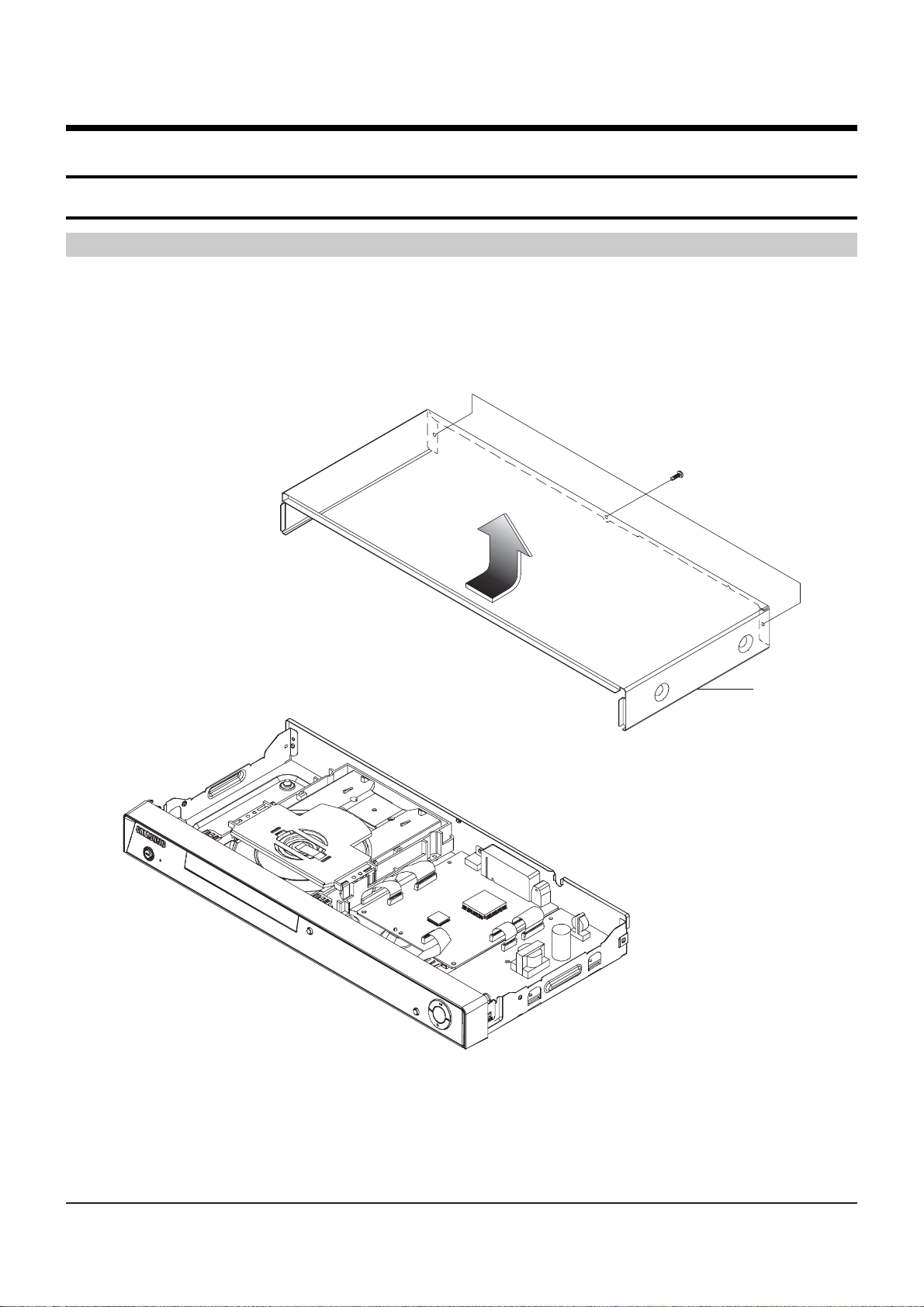
4-1-1 Top Cabinet Removal
1) Remove 3 Screws Πthe back Top Cabinet.
2) Lift up the Top Cabinet in direction of arrow.
Fig. 4-1 Top Cabinet Removal
Note : Reassembly in reverse order.
Π3 SCREWS
( 3 x 10 B )
TOP CABINET
4-2
Samsung Electronics
Disassembly and Reaasembly
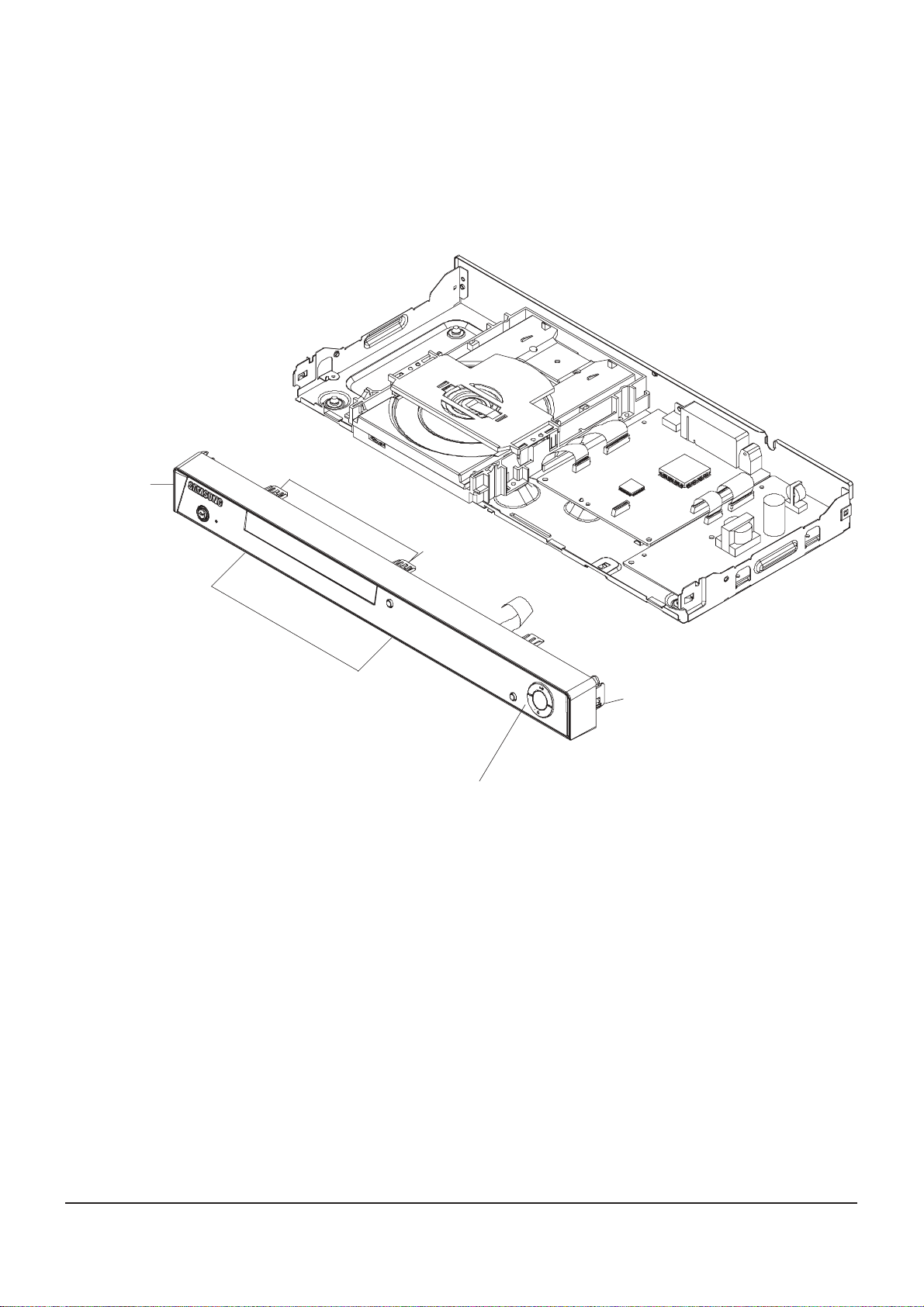
Fig.4-2 Ass’y Front-Cabinet Removal
4-1-2 Ass’y Front-Cabinet Removal
1) Release 6 Hooks Œ, ´, ˇ, ¨ and Remove the Ass’y Front-Cabinet ˆ.
´ 1 HOOK
ˇ 1 HOOK
ˆ ASS’Y FRONT CABINET
Π2 HOOKS
¨ 2 HOOKS
Disassembly and Reaasembly
Samsung Electronics
4-3
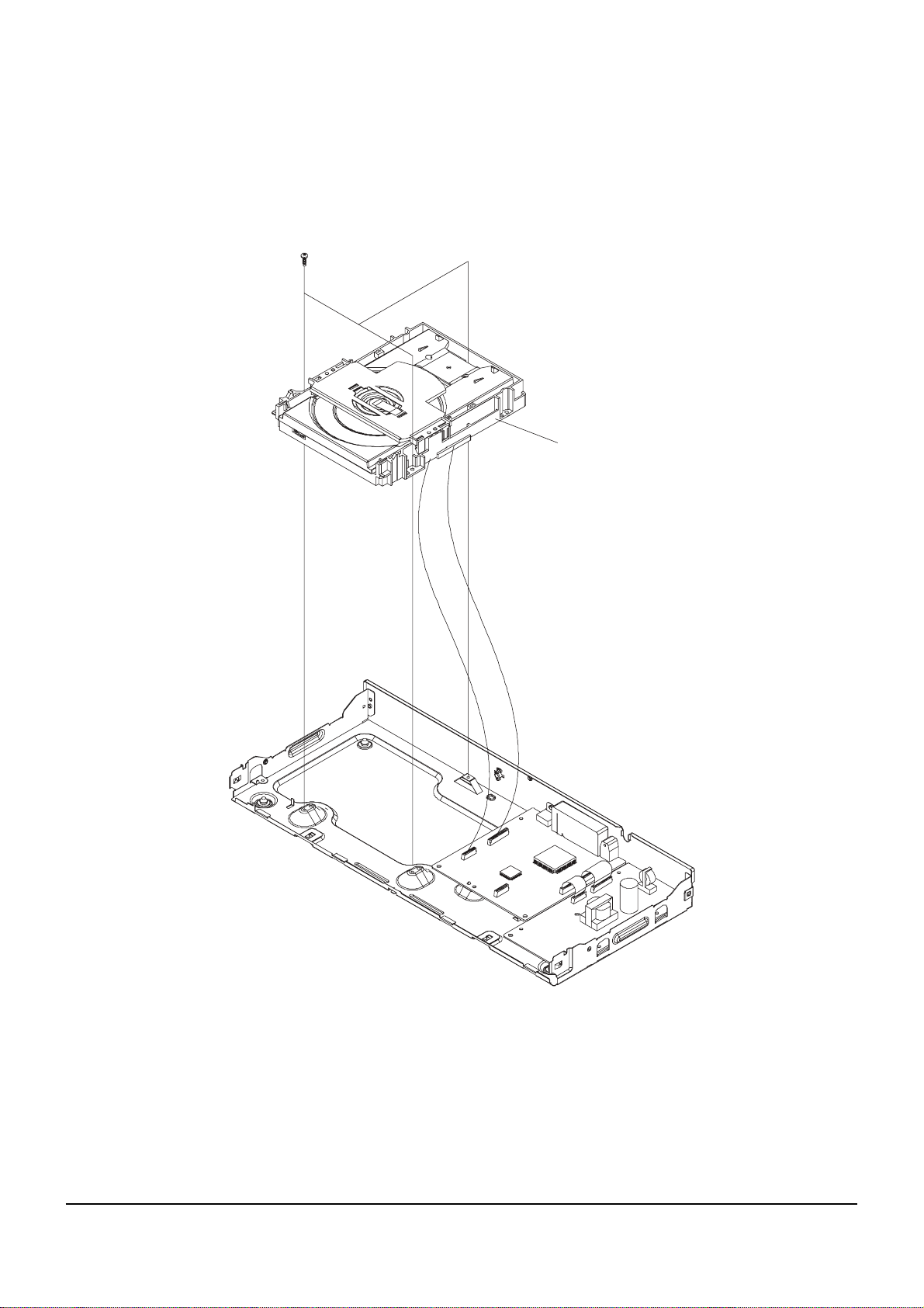
4-1-3 Ass’y Deck Removal
1) Remove 3 Screws Œ from the Ass’y Deck ´ and lift it up.
Fig. 4-3 Ass’y Deck Removal
Π3 SCREWS
( 3 x 6 W )
´ ASS’Y DECK

4-4
Samsung Electronics
Disassembly and Reaasembly
Fig. 4-4 Main PCB and S.M.P.S PCB Removal
4-1-4 Main PCB and S.M.P.S PCB Removal
1) Remove 7 Screws Œ, from the Main PCB & S.M.P.S PCB ´ and lift it up.
Π7 SCREWS
( 3 x 6 W )
´ MAIN PCB & S.M.P.S PCB
Disassembly and Reaasembly
Samsung Electronics
4-5
4-2 Deck
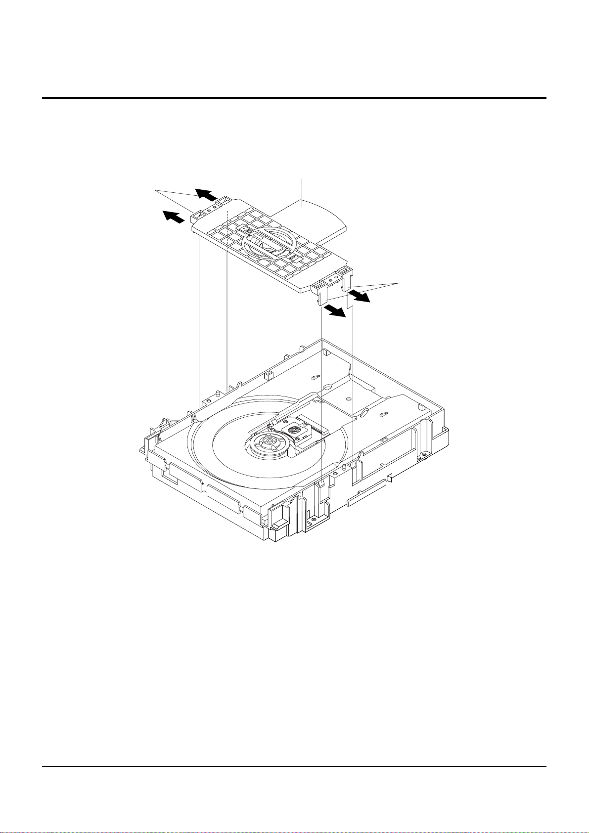
4-2-1 Holder Chuck Removal
1) Push 4 Hooks Œ in the direction of arrow “A” and lift up the Holder Chuck ´.
Fig. 4-5 Holder Chuck Removal
´ HOLDER CHUCK
Π2 HOOKS
Π2 HOOKS
”A”
”A”
4-6
Samsung Electronics
Disassembly and Reaasembly
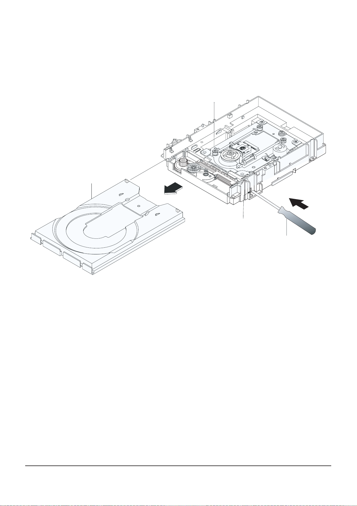
4-2-2 Tray Disc Removal
1) Insert a Screw Driver Œ into Emergency Hole ´ and push the Slider Housing ˇ in the direction arrow “A”.
2) When the Tray Disc ¨ comes out a little, pull it in the direction arrow “B” by hand.
Fig.4-6 Tray Disc Removal
ˇ SLIDER HOUSING
¨ TRAY DISC
´ EMERGENCY HOLE
ΠSCREW DRIVER
“A”
“B”
Disassembly and Reaasembly
Samsung Electronics
4-7
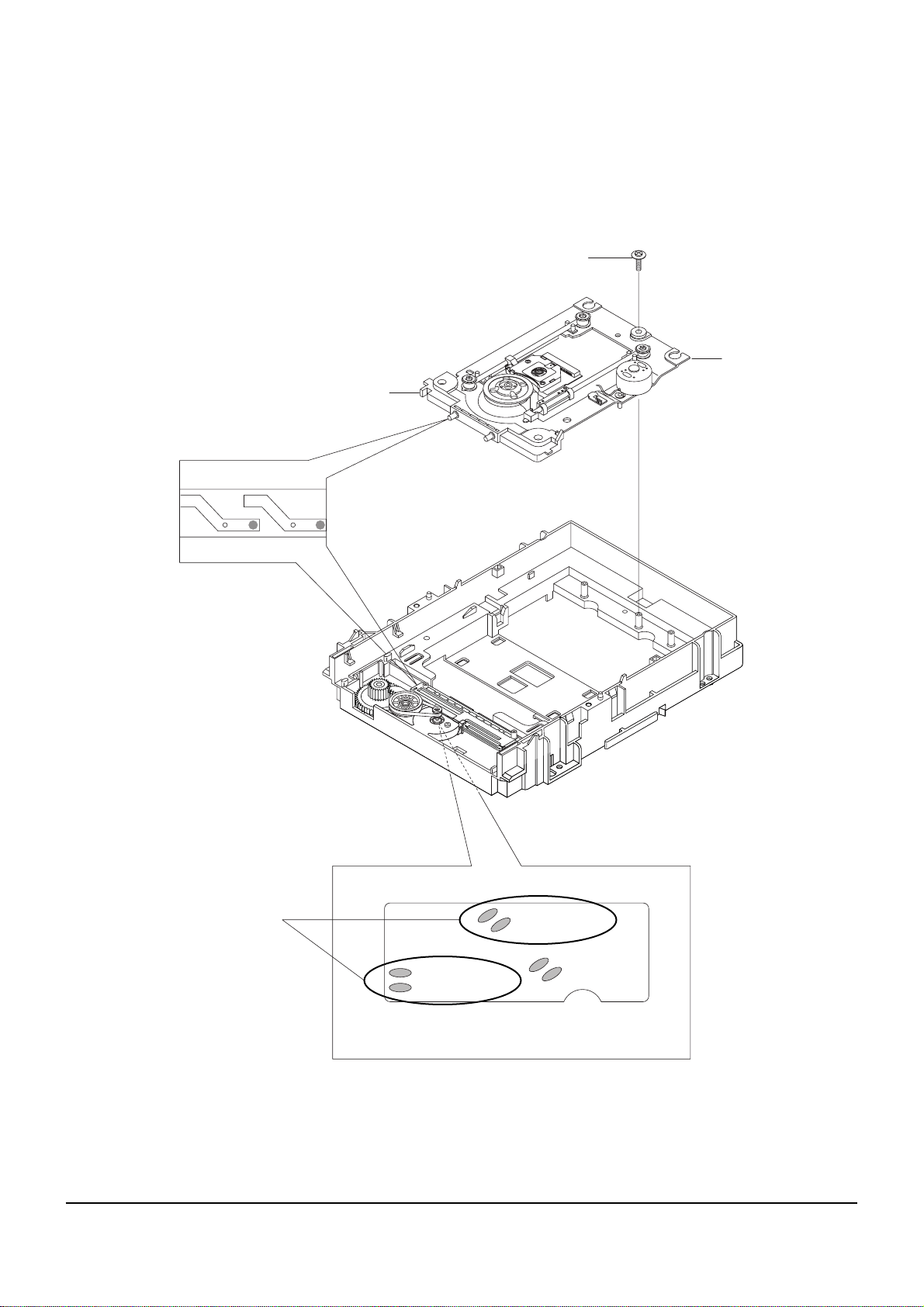
4-2-3 Assy P/U Deck Removal
1) Remove the 4 Soldering Π(SL+, SL-, SP+, SP-).
2) Remove the 1 Screw ´ and lift up the Ass’y P/U Deck ˇ.
Fig. 4-7 Assy P/U Deck Removal
´ 1 SCREW
ˇ ASS’Y P/U DECK
CHASSIS SUB
Π4 SOLDERING
<Assembly Point>
SP + (RED)
SP - (BLK)
SL - (BLK)
SL + (RED)
TM - (BLK)
TM + (BLK)
4-8
Samsung Electronics
Disassembly and Reaasembly
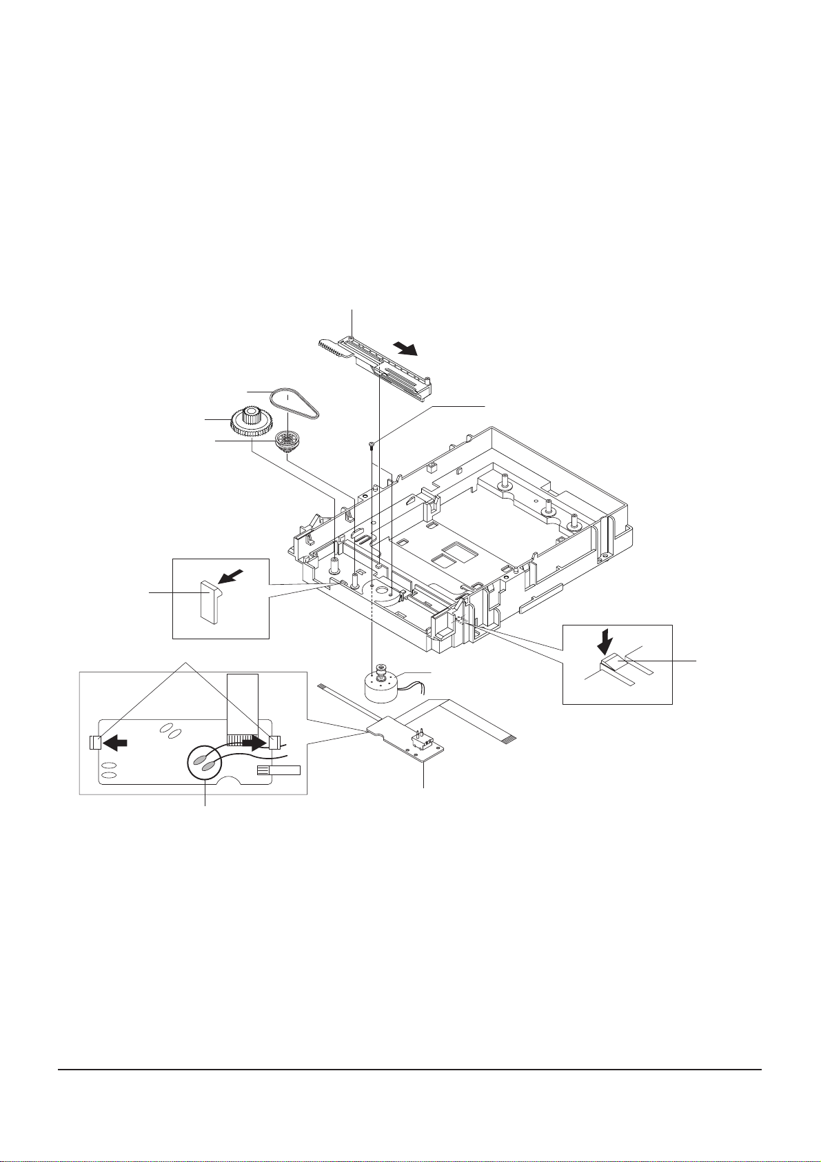
4-2-4 Ass’y Housing Removal
1) Remove the 2 Soldering Œ. (TM+, TM-)
2) Push the 2 Hooks ´ in the direction of arrow “A” and remove Ass’y PCB Deck ˇ.
3) Push the Slider Housing ¨ in the direction arrow “B”.
4) Push the 1 Hook ˆ in the direction of arrow “C” and lift up the Slider Housing ¨.
5) Remove the Belt Pulley Ø and 2 Screws ∏, Ass’y Motor Load ”.
6) Push the 1 Hook ’ in the direction of arrow “D” and lift up the Gear Pulley ˝, Gear Tray Ô.
Fig. 4-8 Ass’y Housing Removal
Π2 SOLDERING
ˇ ASS’Y PCB DECK
ˆ 1 HOOK
” ASS’Y MOTOR LOAD
´ 2 HOOKS
’ 1 HOOK
˝ GEAR PULLEY
Ô GEAR TRAY
Ø BELT PULLEY
∏ 2 SCREWS
¨ SLIDER HOUSING
“B”
“A”
“A”
“C”
“D”
Disassembly and Reaasembly
Samsung Electronics
4-9
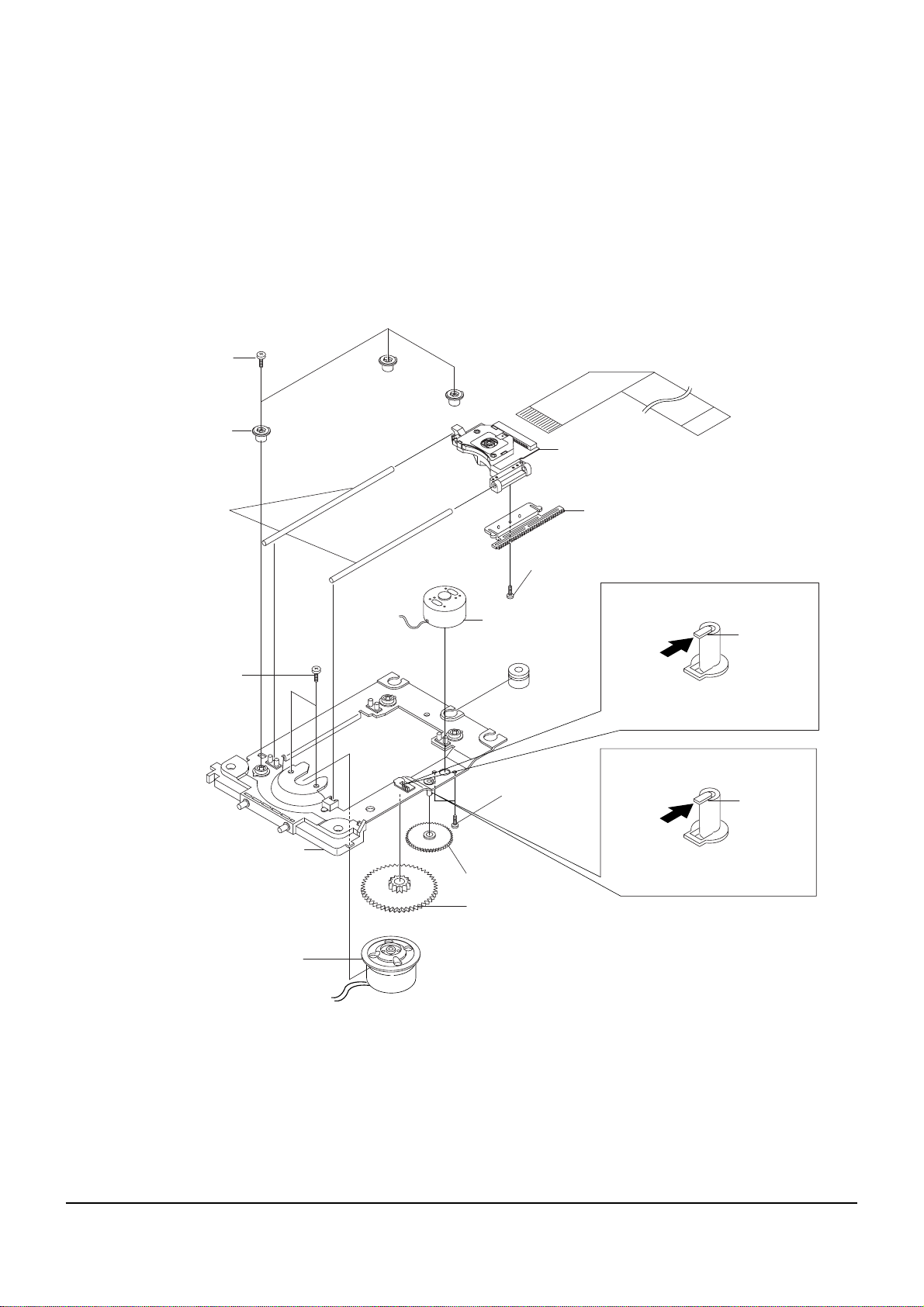
4-2-5 Ass’y Bracket Deck Removal
1) Push the Hook Œ in the direction of arrow “A” and lift up the Gear Feed B ´.
2) Push the Hook ˇ in the direction of arrow “B” and lift up the Gear Feed A ¨.
3) Remove the 2 Screws ˆ and lift up Motor Feed Ass’y Ø.
4) Remove the 2 Screws ∏ and lift down Motor Spindl Ass’y ”.
5) Remove the 3 Screws ’ and remove 3 Holder Cam Skew ˝, Shaft Pick Up Ô, Ass’y Pick Up .
6) Remove the 1 Screw Ò and remove Gear Back Lash Ú.
Fig. 4-9 Ass’y Bracket Deck Removal
ΠHOOK
ˇ HOOK
” MOTOR SPINDLE ASS’Y
´ GEAR FEED B
¨ GEAR FEED A
ˆ 2 SCREWS
CHASSIS SUB
Ø MOTOR FEED
ASS’Y
∏ 2 SCREWS
Ò 1 SCREW
Ú GEAR BACK LASH
ASS’Y PICK UP
Ô SHAFT PICK UP
˝ 3 HOLDER CAM SKEW
’ 3 SCREWS
“A”
“B”

4-10
Samsung Electronics
Disassembly and Reaasembly
MEMO
Samsung Electronics 5-1
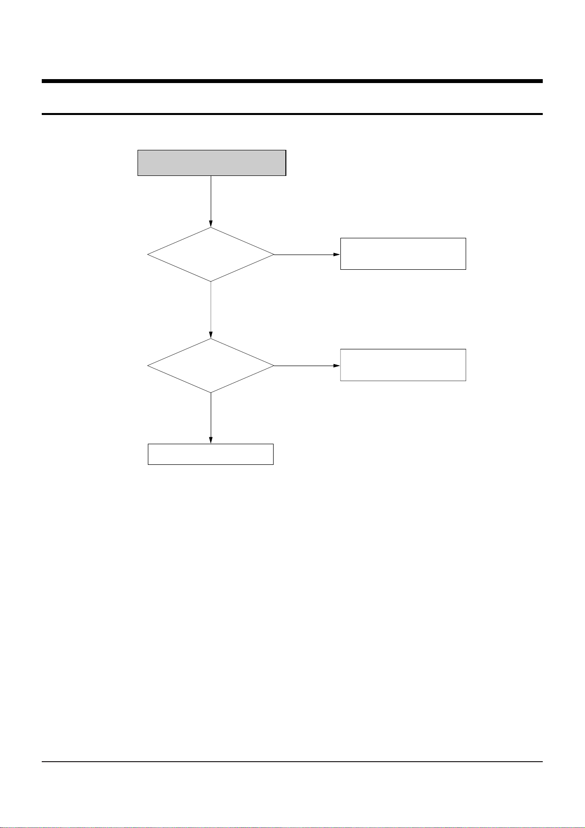
5. Trouble Shooting
No pick-up home positing
ZIC1-187 (SLEDPWM}
output is normal ?
SLED+, SLEDMIC1
- 11, 12 output are normal ?
Check the Sled Motor and
Connection
Check ZIC1.
Check MIC1.
Yes
No
Yes
No
Trouble Shooting
5-2 Samsung Electronics
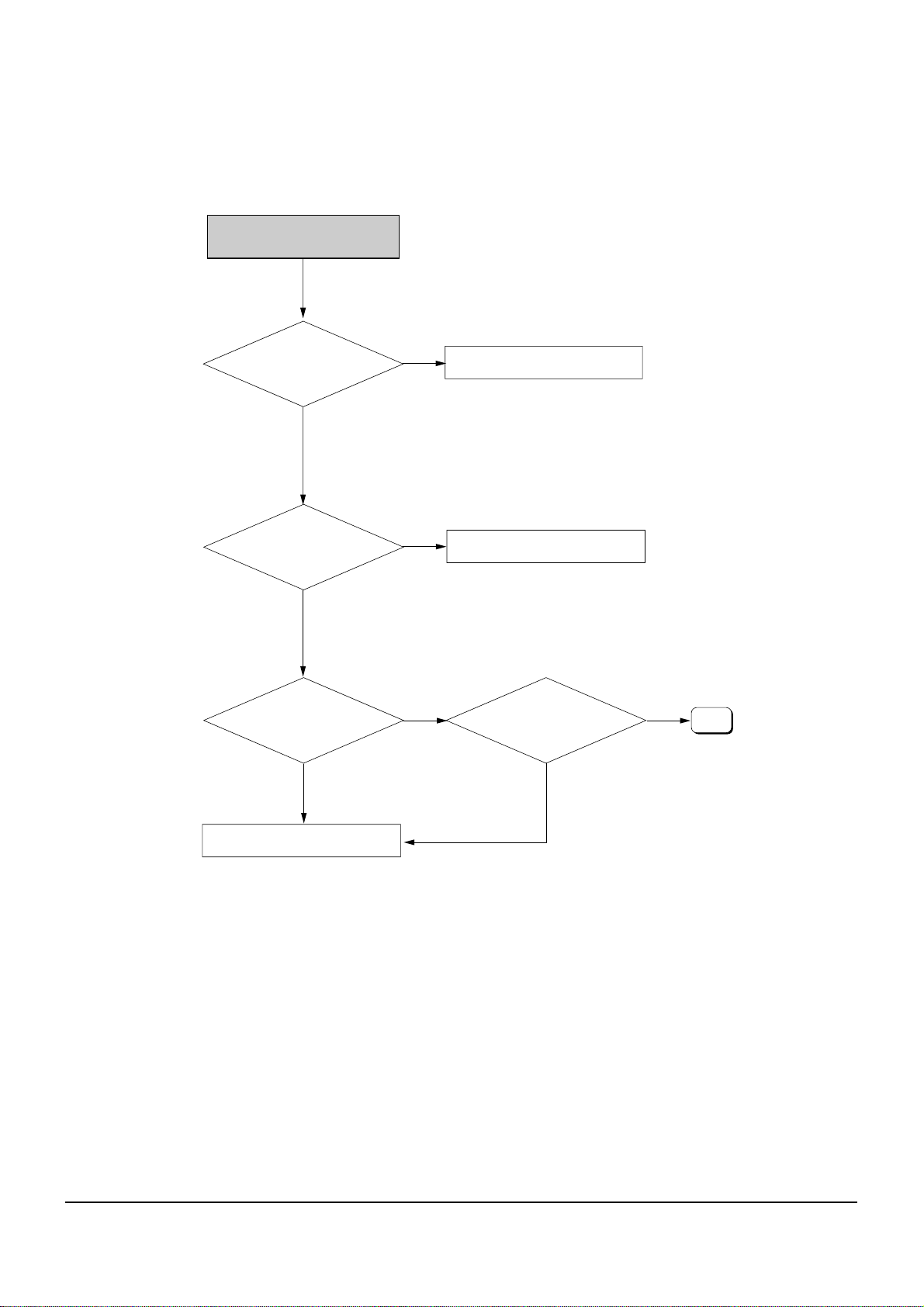
No Search Operation
Actuality occurs
at ZIC1-187 terminal ?
Actuality occurs
at MIC1-11, 12 terminal ?
RF SUM Signal is OK ?
Focus On ?
See "Fine Seek Check"
Check ZIC1 peripharel circuit.
Check MIC1 peripharel circuit
Yes
No
Yes
No
Yes
No
A
Trouble Shooting
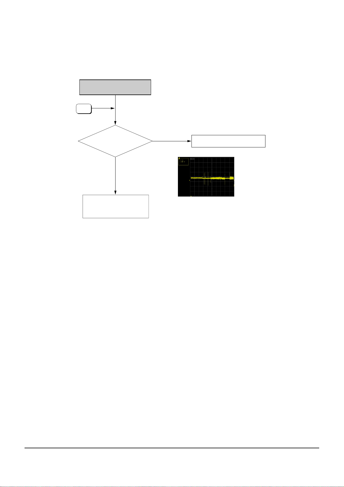
Samsung Electronics 5-3
No Focus incoming
MIC1-13, 14 output
are normal ?
Check MIC1.
Check open state from
MIC1 to Pick-up.
Yes
No
A
(FE Waveform)
 Loading...