

Page 1
Echnbal
Manual
STEREO
DC
INTEGRATED
AMPLIFIER
,F
'1-
.L
;F.t
I
d:,
ff
€.:
I
i:
t,
J
TABLE
Chassis
Ad
Specjf
Addendum
Repair
Schematic
Block
PC
IN
Ch assis-An ordnung
Einstellung
Technische Daten
Nahtrag
Reparaturteilliste
Schaltungsschem a
Blockschaltbild
Besttickungsplane
OF
CONTENTS
(Top
Layout
justmen
t
ications
Parts
List
Diagram
Diagram
Board Diagrams
HALTSVERZE
View)
.
ICHN
(Ob
IS
eransicht)
fr-
"'bo
2
3
6
7
9
. .11
13
. .
. .14
2
3
6
7
9
.
.
11
13
I4
t
THE
FItrITEI-
FlctrEl-
FItrITEI-
EE.,
I-T'D.
E]-EcTFloNlE=i
trIF
ANNEFIIEA,
INC.
cEI.,
l_TD.
1.36-8
OHOKAYAMA,
FLOOR,
2ND
NANKTNG E
1055
SAW
EVERGLORY
ROAD,
MILL
RIVER
Serial
NB80195
MEC
URO-KU,
BLDG.,
TAtpEt;
ROAD,
No.
TOKYO
NO
TAtWAN,
ARDSLEY,
Beginning
152,
305,
SECTION
REpUBLtC
Y
N
JAPAN
OF
10502,
3,
CHTNA
US A
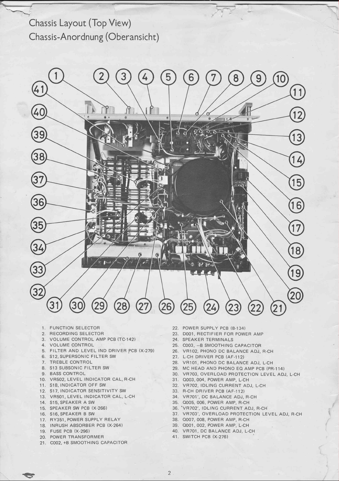
Page 2
F.
*,=.*
f*-
\n-
\F\
-,&'\-"/'--
CF
:,
Chassis
Layout
Chassis-An ordn
(Top
ung
View)
(O
b'e rans icht)
€
FUNCTION
1.
RECORDING SELECTOR
2.
VOLUME CONTROL
3.
4. VOLUME
FILTER
5.
6. S1 2,
TREBLE CONTROL
7.
513
8.
BASS CONTROL
9.
V R502,
1
O.
11. 518,
S17,
12.
VR501,
13.
14. S15,
SPEAKER
15.
516,
16.
RY351
17.
IN R
1
8.
FUSE PCB
19.
POWER TRANSFORMER
20.
COO2,
21.
SELECTOR
CONTROL
AND LEVEL
SUPERSON
SUBSONIC
E
LEV
INDICATOR
INDICATOR SENSITIVITY
LEVEL
SPEAKER
SW
SPEAKER
POWER
,
ABSORB
USH
(X.296)
+g
SMOOTHING
PCB
AMP
IND DRIVER PCB
IC F
I LTER SW
FILTER
IN
L
INDICATOR CAL,
A
PCB
B
SUPPLY
SW
ICATOR
D
OFF SW
SW
(X-266)
SW
RELAY
ER PCB .X-264l.
CAPACITOR
(TC.142}
L,
CA
SW
R.CH
L-CH
\.
V.279t.
POWER
22.
DOO1 , R ECTIF
23.
SUPPLY
PCB
IER FOR
24. SPEAKER TERMINALS
_B
COO3,
25.
VR102,
26.
L-CH DR tVER
27.
VR101
28.
MC HEAD
29.
30. VR7O3,
31. OOO3,
VR7O2, IDLING
32.
R-CH
33.
VR7O1" DC
34.
OOO5,
35.
.VR7O2"
36.
VR7O3"
37.
OOO7,
38.
OOO1,
39.
40.
VR7O1
41
.
SW|TCH
SMOOTHING
PHONO
PHONO
,
DC
PCB
DC
BALANCE
(AF-1
BALANCE
AND PHONO
OVER LOAD PROTECTION
POWER
OO4,
DR
IVER PCB
POWER
006,
IDLING
OVERLOAD
POWER
OO8,
POWER
OO2,
DC BALANCE
,
PCB
AMP,
CURRENT ADJ,
(AF-1
BALANCE
AMP, R-CH
CURRENT ADJ, R-CH.
AMP, R.CH
AMP,
x-276)
(B-1
34)
POWER
CAPACITOR
AMP
ADJ, R.CH
12)
ADJ,
EO
AMP PCB
L.CH
1
L.CH
2)
ADJ, R.CH
PROTECTION
L-CH
ADJ, L.CH
'
L-CH
(PR
LEVEL
LEVEL
-114l'
ADJ,
ADJ, R-CH
L.CH
Page 3
Adjustmenr
lnstruments:
meter,
First
set
'Power,
lector
Se
Turnover
Tape
Function
Phono
Mode
Capacitance
Balance,
Volume control
Phono
A.
Connect
1 .
Monitor
Phono-l
seconds
Feed
2.
Generator,
output
connected
meter
board
un
are
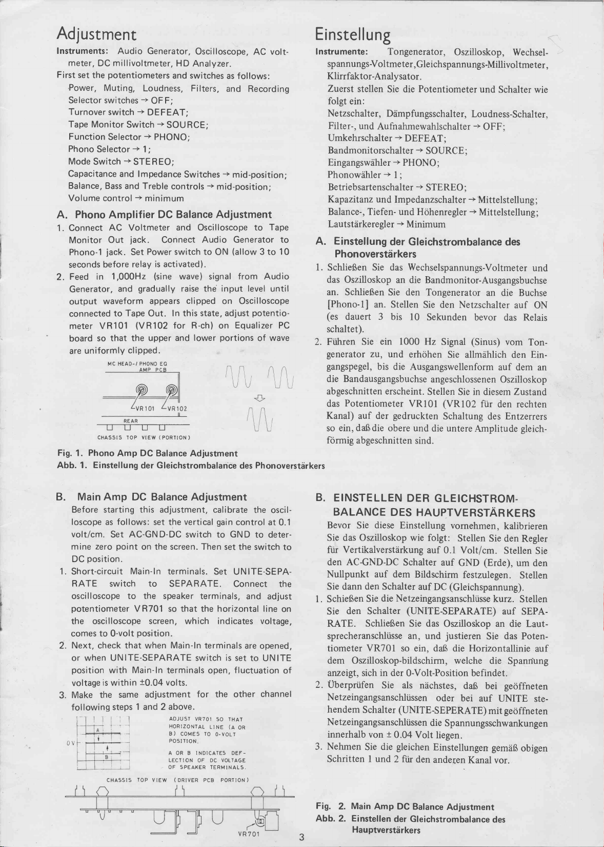
Fig.
1.
Abb. 1.
Audio
m illivoltmeter,
DC
potentiometers
the
Muting,
switches
switcfi
Monitor
Selector
Selector
-+
switch
and lmpedance
Bass
and Treble
Amplifier
AC
Out
jack.
before
1,000H2
in
and
waveform
Tape
to
VR101
so that
ly cl
if
orm
REAR
cHASSTS
Phono
Amp DC Balance
Einstellung
Switch
TOP
Generator,
H D
and
Loudness, Filters,
+
F;
QF
+
DEFEAT;
+
SOU RCE.
pHONO;
+
+
1;
R
sTE
Eo;
Switches
+
controls
minimum
DC Balance
Voltmeter
jack.
Set
relay
gradually
(VR102
the
pped
i
VrEW
der
and
Connect
Power switch to
is activated).
(sine
wave)
raise the
appears
ln this
Out.
for
upper and
.
(
PORTTON
Gleichstrombalance
Oscilloscope,
An
alyzer
.
switches
as
follows:
and
-+
6id-position;
+
6id-position;
Recording
Adiustment
Oscilloscope
Audio Generator to
(allow
ON
from Audio
signal
input level
clipped
on Oscilloscope
state, adiust
R-ch) on
portions
lower
Equalizer
tl'/
)
Adjustment
des
volt-
AC
Tape
to
10
3 to
until
potentio-
PC
wave
of
tA
Phonoverstdrkers
Elnstellung
lnstrumente:
sp annungs
Klirrfaktor-An
Zuerst
folgt
ein:
Netzschalter,
Filter-,
Umkehrschalter
Bandmonitorschalter
Eingangswdhler + PHONO
Phonowdhler
Betriebsartenschalter
Kapazitanz
Balance-, Tiefen-
Lautstdrkeregler
Einstellung
A.
Ph
on overstd rke rs
1.
SchliefJen Sie das
das oszilloskop
an. Schlief3en
[Phono-
(es
dauert 3
schaltet).
2. Fiihren
generator
gangspegel,
die Bandausgangsbuchse
abgeschnitten erscheint.
Potentiometer
das
Kanal)
dafJ
ein,
so
formig
abgeschnitten
Tongenerator,
-Vol
tme te
alysator
stellen
Sie die
Ddmpfungsschalter,
und
Aufnahmewahlschalter
+
+
I
i
und
Impedanzschalter
und Hohenregler
+
der
an die Bandmonitor-Ausgangsbuchse
Sie den
lJ
an. Stellen
bis
ein 1000
Sie
zv,
und
bis die
auf der
gedruckten
die obere
Oszilloskop,
r,
ichsp
Gle
.
Potentiometer
DEFEAT;
+
-+
Minimum
Gleichstrombalance
Wechselspannungs-Voltmeter
l0
erhohen
Ausgangswellenform
VRl0l
und
sind.
annung
s-Millivol
und
Schalter wie
Loudness-schalter,
+
OFF;
SOURCE
STEREO
Tongenerator
Sie den Netzschalter
Sekunden
Hz
;
Signal
;
;
+
Mittelstellung
+
Mittelstellung;
an die Buchse
bevor das
(Sinus)
Sie allmdhlich
auf dem
angeschlossenen
Stellen
Sie
(VRl02
Schaltung
untere
die
Oszilloskop
in
diesem
ftir
den rechten
des
Amplitude
des
vom
Entzeners
Wechsel-
tme
te
;
und
auf
ON
Relais
Ton-
Ein-
den
an
Zustand
gleich-
r,
Main Amp
B.
DC
Balance Adjustment
Before starting this adjustment, c0librate
loscope
volt/cm.
mine
DC
1.
Short-circuit
R ATE
oscilloscope
potentiometer
the oscilloscope
comes
Next, check that when
2.
as
Set
zero
position.
switch
to
0-volt
follows:
point
set
the
AC-GND-DC switch
on the screen. Then
Main-ln
to
terminals.
PA
SE
to the speaker
R701
V
position.
so that
screen, which indicates
Main-ln
vertical
RATE.
terminals,
the
terminals
or when UNITE-SEPARATE switch
position
voltage
Make
3.
following
with Main-ln
is
within
same
the
1
steps
TOP
CHASSIS
terminals
10.04
volts.
adjustment
above.
2
and
ADJUST
HoRIzoNTAL
B)
POSt Tt
A
OR B
LECTION
OF SPEAKER
(
V IEW
DRIVER PCB PORTION
for
VR7Ol
COMES TO
ON
INDICATES
OF
open,
LINE
DC
TERMINALS.
the
gain
control
GND
to
set the switch
Set
ITE-SEPA-
UN
to deter-
Connect
and
horizontal line
voltage,
are
opened,
is
set
to
UNITE
fluctuation
channel
other
the
THAT
SO
(a
on
O-VOLT
DEF-
VOLTAGE
)
oscil-
at
0.1
the
adjust
on
B.
EINSTELLEN
BALANCE
Bevor
to
Sie das oszilloskop wie
fiir Vertikalverst[rkung
den
Nullpunkt auf
dann
Sie
1. SchiefJen
Sie
RATE.
sprecheranschliisse
tiometer
of
dem
arzergt, sich
2.
Uberpri.ifen
Netzeingangsanschli.issen
hendem
Netzeingangsanschltissen
innerhalb
3. Nehmen
Schritten
diese
Sie
AC-GND-DC
den
Sie
den
Schalter
SchliefJen
VR701
Oszilloskop-bildschirm, welche
Schalter
von
Sie
I und
DER
GLEICHSTROM.
DES
HAUPTVERSTAR
Einstellung
folgt:
auf
0.1
Schalter auf
dem
Bildschirm
Schalter
die
auf
Netzetngangsanschltisse
(UNITE-SEPARATE)
Sie
8o,
so ein, dafj
in der
O-Volt-Position befindet.
Sie als
(UNITE-SEPERATE)
t
0.04
Volt
gleichen
die
fift
2
den
(Gleichspannung).
DC
das
Oszilloskop
justieren
und
nf,chstes,
oder
die
Spannungsschwankungen
liegen.
Einstellungen
anderen
vornehmen,
Stellen
Sie den
Volt/cm.
(Erde),
GND
festzulegen.
kurz.
Sie
Horizontallinie
die
die
dafJ
bei geoffneten
bei
auf
mit
gemd3
Kanal
KERS
kalibrieren
Stellen
um den
auf
an
die Laut-
das
Spannung
UNITE
geoffneten
vor.
Regler
Sie
Stellen
Stellen
SEPA-
Poten-
auf
ste-
obigen
Fig.
Abb.
Main
2.
Einstellen
2.
Hauptverstd
Amp DC
Balance
der Gleichstrombalance
rkers
Adjustment
des
Page 4
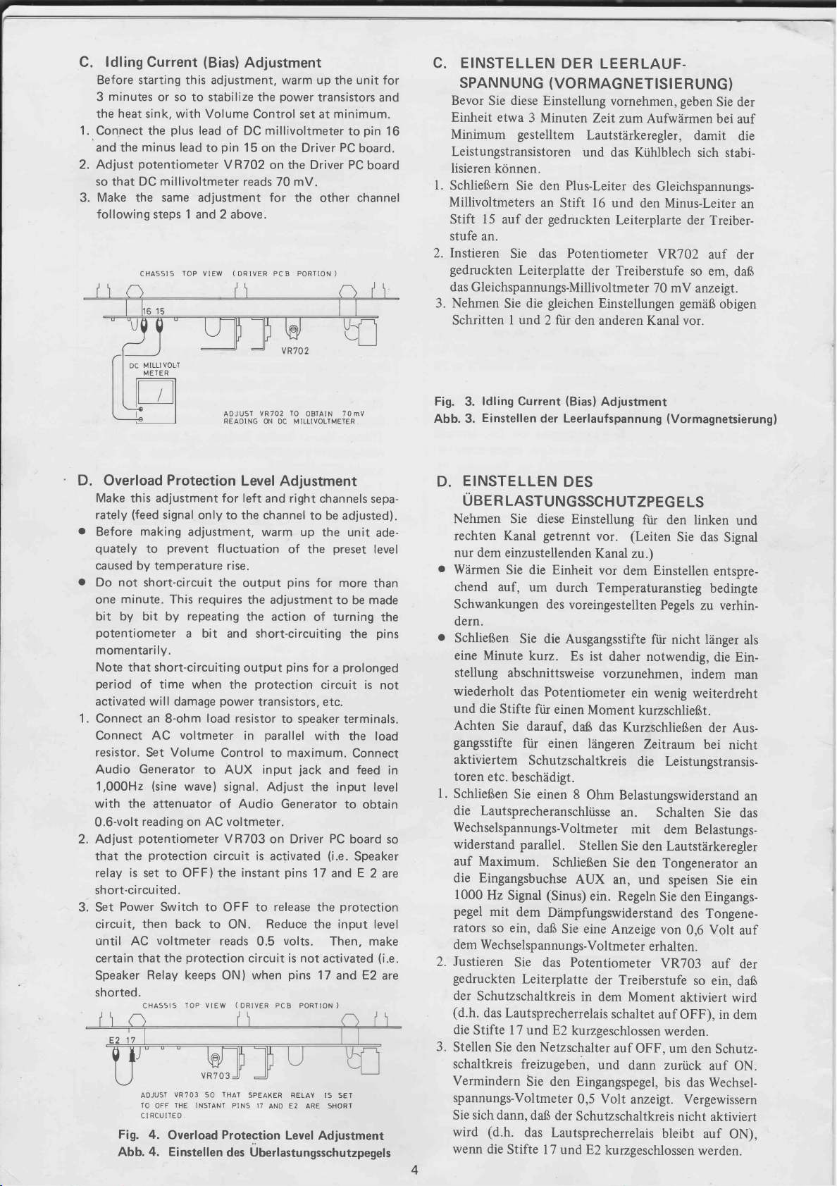
ldling
C.
Before starting
3
the
1.
Connect the
and the
2. Adjust
so that DC
Current
minutes
heat
sink,
minus lead
potentiometer
3. Make the
following
CHASSIS
MILLI
METER
(Bias)
Adjustment
this adjustment, warm up
or so
to stabilize the
with Volume
plus
lead
to
millivoltmeter
same
adjustment
steps 1 and 2 above.
TOP
VIEW
VOL.T
Control
DC
of
pin
15
VR7O2
reads
(
DRTVER
power
transistors
set
at
millivoltmeter
on
Driver
the
on the Driver
mV.
70
for
the other
PCB PORTION
unit for
the
minimum.
pin
to
PC
board.
PC
board
channel
)
and
16
C.
EINSTELLEN
SPANN
Bevor
Einheit etwa
Sie
UNG
diese
Minimum gestelltem
Leistungstransistoren
lisieren
1.
SchliefJern
Millivoltmeters
Stift
stufe
Instieren
2.
gedruckten
das Gleichspannungs-Millivoltmeter
3. Nehmen
konnen.
15
an.
Schritten
Sie den
auf
Sie
Leiterplatte
Sie
und
I
DER
LEERLAUF.
(VORMAGN
Einstellung
3 Minuten
Zeit
Lautstdrkeregler,
und
Plus-Leiter
an
Stift 16 und
gedruckten
der
das Potentiometer
der
gleichen
die
fur
2
Einstellungen gemdfJ
den
anderen Kanal
ETISI E
vornehmen,
zum
Aufwdrmen
das
Ktihlblech
des
Gleichspannungs-
den Minus-Leiter
Leiterplarte
VR702
Treiberstufe
70 mV
RUNG)
geben
damit
sich stabi-
der
Treiber-
auf der
effi,
so
anzergt.
vor.
Sie der
bei
auf
die
an
dafJ
obigen
D. Overload
Make
rately
o
Before
quately
caused by
o
not
Do
minute.
one
Protection
adjustment for left
this
(feed
signal
making
prevent
to
temperature
short-circuit
This requires
bit by bit by
potentiometer
momentarily.
Note
that short-circuiting
pe
riod
of time wh
activated will
1 .
Connect
Connect
resistor.
Audio
1
,000H2
with the attenuator
0.6-volt
2. Adjust
that the
relay
sh ort-ci
3. Set
circu
until AC
certain that the
Speaker
sh o
an
AC
Set
Generator
(sine
reading
potentiometer
protection
is set
ited
rcu
Power
Switch to OFF to
it,
then back to
voltmeter
Relay keeps
rted .
cHASStS
ADJUST
TO
OFF
CIRCUITED
Fig.
4.
4.
Abb.
8-ohm
Volume
to
Overload
Einstellen
ADJUST VR7O2
READING
Level
only to
the
adjustment,
f
luctuation
rise.
the
output
TO
OBTAIN
ON DC
M ILLI
Adjustment
and right
channel
warm up
of the
pins
to be
the adjustment
repeating
the
action
a bit and short-circuiting
pins
output
en the
damage
load resistor
voltmeter
to
wave
protection
power
transistors, etc.
parallel
in
Control to
AUX input
signal. Adjust
)
to speaker
max
jack
the
of Audio Generator
voltmeter.
on AC
circuit is
F
the
OF
)
.
reads
protection
ToP
VIEw
VR7O3 SO
THE INSTANT
VR703
ON) when
THAT
Protection
des Uberlastungsschutzpegels
on Driver
activated
.
0.5
pins
release
Reduce
volts.
instant
ON
circuit is
pins
(
onlven PcB PoRTIoN
SPEAKER
AND
RELAY 15
E2
Level
PINS 17
not
ARE
7O mV
VOLTMETER
channels
adjusted).
the unit
preset
for
more
to
be
rn
of tu
ing
the
prolonged
for
a
ci rcu it
terminals.
with
the
imu m.
Connect
feed
and
input
to
PC
board
(i.e.
Speaker
17
the
E
and
protection
the
put
in
Then, make
activated
17
and
)
5ET
SHORT
Adjustment
sepa-
ade-
level
than
made
the
pins
is
not
load
level
obtain
2
are
level
(i.e.
E2
are
Fig.
Abb. 3.
D.
o
o
in
l.
ldling Current
3.
Einstellen
EINSTELLEN
UAE R LASTUNGSSCH
Nehmen
rechten
nur
wdrmen
chend
Schwankungen
dern.
Schlie8en
eine
stellung
wiederholt
und
Achten
gangsstifte
aktiviertem
toren
SchliefJen
die
Sie
Kanal
dem
einzustellenden
Sie
auf,
Sie die
Minute
abschnittsweise
das
die
Stifte
Sie
fiir einen
etc.
beschddigt.
Sie
Lautsprecheranschli.isse
wechselspannungs-voltmeter
so
widerstand
auf
Maximum.
die
Eingangsbuchse
1000
pegel
rators
dem
We
Justieren
2.
gedruckten
der
Schutzschaltkreis
(d.h.
das Lautsprecherrelais
die
Stift
3.
Stellen
schaltkreis
Hz
Signal
mit
so ein,
chselsp
Sie das
e
17 und E2
Sie
parallel.
dem
Leiterplatte
den
freizugeben,
vermindern
spannungs-Voltmeter
Sie sich dann,
(d.h.
wird
wenn
die
Stift
(Bias)
AOjustment
der
Leerlaufspan
DES
UT
diese
Einstellung
getrennt
die
Einheit
um
des
kurz.
vor.
Kanal
vor
durch
Temperaturanstieg
voreingestellten
Ausgangsstifte
Es ist
daher notwendig,
vorzunehmen,
Potentiometer
fiir einen
darauf,
Moment
da8
das
ldngeren
Schutzschaltkreis
einen
8
Ohm Belastungswiderstand
Stellen
Schlie8en
(Sinus)
Diimpfungswiderstand
da8
Sie eine
annungs-Voltmeter
AUX
ein.
Sie den
&o,
Regeln
Anzeige
Potentiometer
der
Treiberstufe
in
dem
schaltet
kurzgeschlossen
Netzschalter
auf
und
den
Sie
dafJ
das
e
Eingangspegel,
0,5
Volt
der
Schutzschaltkreis
Lautsprecherrelais
17
und E2
kurzgeschlossen
(Vormagnetsieru
nu
ng
ZPEG
E LS
ftir den linken
(Leiten
zu.)
dem Einstellen
ftir nicht liinger
ein
wenig
kurzschliefJt.
Kurzschlie8en
Zeitraum
Sie
Pegels
das
bedingte
zv verhin-
indem
weiterdreht
der Aus-
bei
die Leistungstransis-
an.
Schalten
mit
dem Belastungs-
Sie den
Lautstdrkeregler
Tongenerator
und
speisen
Sie
den
des
von
0,6 vqlt
erhalten.
VR703
so ein,
Moment
oFF,
aktiviert
auf
oFF), in
werden.
uffi
den
dann zuri.ick
bis das
anzeigt
Vergewissern
nicht
bleibt
Eingangs-
Tongene-
auf
wechsel-
aktiviert
auf
werden.
und
Signal
entspre-
als
die
Ein-
man
nicht
an
Sie
das
an
Sie
ein
auf
auf der
da3
wird
dem
Schutz-
oN.
oN),
ng
)
Page 5
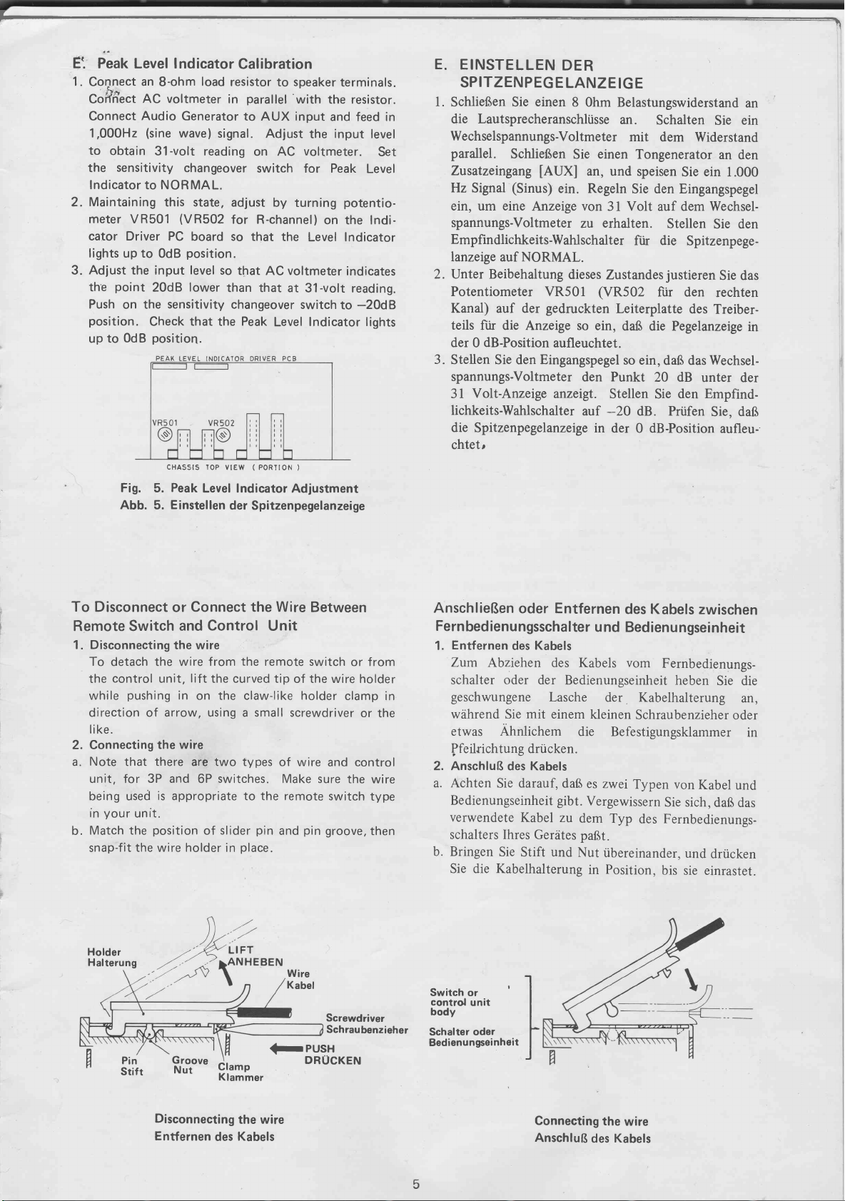
Er.
Peak Level
1.
Corynect
Cofrfi'e.t
Connect
1,000H2
to
obtain
sensitivity
the
icator
lnd
Maintaining
2.
meter
cator Driver
lights
Adiust
3.
point
th'e
Push
position.
to
up
Abb.
lndicator
an
8-ohm
AC voltmeter
Audio
(sine
31-volt reading
to N
O
this state,
R
V
501
PC
up to
0dB
the input
20dB
on the
OdB
Fig.
sensitivity
Check
position.
CHASSIS TOP
Peak
5.
Einstellen
5.
load
resistor
in
Generator
wave)
signal.
changeover
R MA L.
adjust
(V
R502
for R
board so
position.
level
so
lower
than that
changeover
that
the
VIEW
Level lndicator
der
Calibration
speaker
to
parallel
'with
to AUX input
Adjust
the
on AC
switch
that the
that
Peak
(
PORTION
Spitzenpegelanzeige
voltmeter.
for Peak
by
turning
-channel
voltmeter
AC
at
31-volt reading.
switch
Level
)
Adiustment
on
)
Level lndicator
lndicator lights
terminals.
the resistor.
and
feed in
input
level
Set
Level
potentio-
the lndi-
indicates
to
-20dB
E.
EINSTELLEN
SPITZENPEG
l.
Schliefjen Sie
DER
E LANZEIG
einen
8
die Lautsprecheranschliisse
wechselspannungs-Voltmeter
parallel.
Zusatzeingang
Hz
ein, um eine
spannungs-Voltmeter
Empfindlichkeits-Wahlschalter
lanzerge
2. Unter Beibehaltung
Potentiometer VR501
Kanal)
teils
der
3.
Stellen
spannungs-Voltmeter
3I
lichkeits-Wahlschalter
die
chtet,
Schlie8en
Sie
[AUX]
(Sinus)
Signal
auf NORMAL.
auf der
ftir die
dB-Position
0
Sie den
Volt-Anzetge
Spitzenpegelanzeige
ein. Regeln
Anzeige
dieses
gedruckten
Anzeige so
aufleuchtet.
Eingangspegel
anzergt
zv
E
Ohm Belastungswiderstand
an.
mit
einen
Tongenerator
&tr, und
von
speisen
Sie den Eingangspegel
Volt
31
erhalten.
ftir die
Zustandes
(VR502
Leiterplatte
ein,
dafJ die
so ein,
den Punkt
Stellen
auf
in
dB. Priifen
-20
der
0
Schalten
dem
auf dem
Stellen
justieren
fiir
dafJ das Wechsel-
20
Sie
dB-Position
Sie
Widerstand
an
ein
Sie
Wechsel-
Sie
Spitzenpege-
Sie
den
rechten
des
Treiber-
Pegelanzeige
dB
unter
Empfind-
den
Sie, dafj
aufleu-
an
ein
den
1.000
den
das
in
der
To Disconnect
Remote Switch
1. Disconnecting
To
detach
the
while
direction of
like.
2. Connecting
Note
a.
unit, for
being used
you
rn
Match
b.
snap-fit
Holder
Halterung
the wire from
control
pushing
there
that
unit,
the
3P and
is appropriate to the remote
tt.
r un
position
the
the wire holder in
Pin
Stift
Connect the Wire
or
and Control
the wire
the
lift
the curved tip
in
on the claw-like
arrow, using
wire
are two types
6P
G
roove
Nut
switches.
slider
of
place.
H
Clamp
Klammer
a
Between
Unit
remote switch
of the wire
holder
small
screwdriver
of wire
Make sure
pin
pin
and
Wire
Kabel
fTPUSH
DRUCKEN
or from
holder
clamp
in
or
the
control
and
the wire
switch
type
groove,
Screwdriver
Schraubenzieher
then
AnschlieBen
oder
Entfernen
Fernbedienungsschalter
Entfernen
1.
zum
Abziehen des
schalter
geschwungene
wdhrend
etwas
ffeilrichtung
2. AnschluB
a. Achten
Bedienungseinheit gibt.
verwendete
schalters Ihres
b. Bringen
Sie die Kabelhalterung
Switch
or
control
unit
body
Schalter
Bedienu
oder
ngseinheit
Kabels
des
oder
der
Lasche
mit
Sie
einem
Ahnlichem
drticken.
des Kabels
darauf,
Sie
Kabel
Gerdtes
Sie
Stift und
Bedienungseinheit
dafJ
zu
des Kabels
u nd
Bedienungseinheit
Kabels vom
zwischen
Fernbedienungs-
heben
Sie die
der Kabelhalterung
kleinen
Schraubenzieher
die Befestigungsklammer
es zwei
Vergewissern
dem
pa8t.
Nut
in
Typen
Sie sich,
Typ
tibereinander,
Position,
Fernbedienungs-
des
bis
von
Kabel
dafJ
und
drucken
sie einrastet.
on,
oder
in
und
das
Disconnecting
Entfernen
des
the wire
Kabels
Connecting
AnschluB
the
des
wire
Kabels
Page 6

Specifications
Technische
Daten
POWER
A.
r
Continuous
Total
r
lntermodulation
AMPLIFIER
Power
Harmonic
(60H2:7,000H2-4:11
t
Frequency
r
lnput
Output
Damping
r
Hum
r
Crosstalk,at
EOUALIZER
B.
tape
r
Output
r
Harmonic
r
Phono
Response
+OdB
DC lN,
+OdB
DC lN,
+OdB
lN,
AC
Sensitivity/tmpedance
Speaker
;
Factor
at 20Hz
at
-
1000H2
Noise
and
lo,OoOHz : :
out
)
Voltage/lmpedance
Rated Output
PIN Jack .
lN Jack .
D
Max.
Output at
Jack
PIN
Distortion
Phono-l
Phono-3
-2
,
(MC)
Equalization
Phono-1,-2,-3
r
H um
lnput
Noise
and
Phono-1
Phono-3
-2
,
(MC)
Sensitivity/tmpedance
Phono-1
P,hono-2
Phono-3
Crosstal
Overload
Phono-1
Phono-3
(MC)
k
at 20,000H
at 1
-2
,
(MC)
SECTION
Output
Distortion
Distortion
(at
1-watt output)
-
-1dB
-
-3dB
dB 5Hz
-
-1
B
. .A or
A+B
2O,000H2
. 65
.
(lH
F
A-network)
. : :l3gt
:
AMPLIFIER
at
THD
0.5%
.
.
(SV-outpu
. 0.006%
z
20H
to 2O,000H2
(
F
| H
A-Networ k, 1
(MAG)
.
.
at rated
.
z
z
TH
.5o/o
O
,000H
.
120W*
RMS,
at B-M
20,000H2 with
0.01 % total
tton.
No more
outpu t.
No more
watt
No more
watt output.
No more
watt output.
No more
watt
4Hz
2Hz
1 .5V/50kC)
4
8
100
SECTION
1,000H2
150mV
per
both
load, from
than 0.01o/odt
t
than
output.
than
than 0.01 5% at 60-
than
output.
100,000H2
-
200,000H2
-
100,000H2
-
16S)
-
16Sl
-
(measured
l2k{t
channels driven
harmon
50mV/80ko
25V
t, 2OHz to 20,000H2)
0.005%
STD
outpu t)
/35kO,
t
RIAA
-V
75dB
64dB
output
2mV
1
00, Z00pF
2mVl50k4
100pV/SSo
B
55d
D
400mV
15mV
channel
2OHz to
no more
ic
0.006%
0.008% at
0.008% at
0.3dB
50kO,
distor-
at
at
OkO,
min.
than
rated
60-
1-
1-
0,
PREAMPLIFIER
C.
r
Output
Voltage/lmpedance
RatedOutput.
Max.
(20H
(+ooB,
and
Output
Distortion
z
to 20,000H2)
Response
dB)
-1
(lHF
Noise
r
Harmonic
r
Frequency
r
Hum
Tuner,AUX..
Tape Monitor-1
Residual Noise
r
lnput
Sensitivity/lmpedan."'..
Tuner'AU.x
monitor-l
Tape
r
Overload
t
Crosstal
r
lntermodulation. Distortion
(1,000H2,O.5o/o
Tuner,
Monitor
Tape
k
AUX
(1
,000H2
-1
60Hz:7,000H2-4:1
D.
CONTROL
r
Tone
Bass
Treble Control
CHARACTERISTIC
Controls
(at
100H2)
Turnover,
Turnover, 400H2
Tu rn
ove
150H2
r,
7,000
Turnover,2,SOOHz
r
Loudness,
r
Superson
r
Subsonic
r
Audio
E. MISCE
r
Power Requirement
r
Power
r
Dimensions
r
Weight(Net)
Note:
at 100H2
10,000H2
at
Filter
ic
Filter
Muting
.
LLANEOUS
Consumption
(Overall)
Specification
notice.
without
*Measured
Regulation
Trade
(Applicable
at 16Hz
pursuant
SECTION
rated
at
.
A-Network)
-2
,
(volume
, - l
(at
at
control
I
,2
THD)
I
'
-2
,
f
)
10,000H2)
z
H
24,000H2
..,
and
design subject to
to
Rule
to the U.S.A.
(measured
1.5V/6004
7V
output
0.008%
4Hz
95dB
95dB
at
;.,:::';ffit
15omv/50k0
15V
TOdB
O.Olo/o
+5d8,
+1
OdB,
+5d
+1
0dB,
+8dB
+4dB
12dBloct
2dBloct
-1
sdB
-1
12OV
.
24OV
220, 240V
(Switchable
.
900 watts
a82JUX)
.
mrfi
22kg
Federal
the
Power
on
ly
on
)
at
tape out)
(O.S%
TH D
)
160,000H2
to
min.)
AVE
-sdB
B
0d
-1
B,
B
-5d
-10d8
t
1dB
tldB
tl
dB
l6OHz,22OV l5OHz,
or 100,
l50Hz,
150
)
max.
x
143(H)
possible
Claim
Trade
modification
Commission's
for
Amplifiers.
12O,
N
60Hz
x 408(D)
Page 7

Addendum
Nachtrag
1 . The overload
change
This
The
N 883986
new
overload
numbers
a)
ment of overload
R746,
tors
0716
are
new unit.
the
Because
b)
of
new Driver
given
ventional Driver
o
new
a
PC
Driver
is
applicable
or over.
o
c) See
ci
To check
d
)
when
pl
newly
The
Board assembly:
Figs.
n
it
rcu
a
d
new
:
oyed
1) Connect
produce
and
signal
wave
Maintaining
2l
E2 on
speaker
Reduce
3)
ma
ce
ke
pins
when
e) To attach
conventional
to
N 883985
PC
Driver
necessary to
are
Fig.
PARTS REOUIRED:
1)
2) Screw
3)
HOW
1)
for
C-2
PC board
M3
Nut,
TO ATTACH
a
Drill
plate.
Attach
2l
Driver
fitting
The
3)
PC
Board as
Fig.
in
2. The
following
units with Serial
Phono-3(MC)
Conventional
input
the
at
unplugged.
New design:
jack
is
Since
to
conventional
is
used to
new type
use the
left
it
or
circu
to
over.
detection
is
applicable
protection
protection.
748 and VR703,
747,
eliminated
the
PC
number, to distinguish
Board assembly
A and
con
operation
Overload
an
D,river
relay
output
rta i n
the
it is necessary
Board
mounting
fi$ng
+
3* 6mm:
Hexagonal
d3.5
See
the Overload
PC
C-3.
modification
input
unplugged.
short
jack
pin plug
iack
from the
modification
Board assembly
PC
Board.
units with serial
to
Part No.
for
the
.
overload
of
Overload
designed
B
nection
Detection
resistor to speaker
load
8S)
0.6-volt
state,
PC
board and
terminals.
short-circuit
speaker
at
)
this
is set to OF
voltage
the
that
E2 are shorted.
17
and
new
Overload
(with
un its
plate.
f itting
the
attach
position.
plate:
Part No. 120012231 .
Part
:
Part
hole in
Fig.
Board
position
No.
design:
terminal
the
with a
the
1 .
C-
Detection
fitting
of
from chassis top
seen
N892399 or
jack
design
the
when the
circuit
input
The
circuit.
the
is available
for
shorting
new
new
output
speaker
to drill
Driver
the Overload
has
input
one.
been
modif ied.
with serial
has
all
units
circuit saves adjust-
Accordingly
.transistor
and
PC
Driver
explained
used for repair
Board of
in 1. a), the
it from con-
(Part
No.
14181 0328)
N883986
nos.
Detection
14181 0850.
overload
protection
PC
F.
to
0.5
Detection
serial
The
new
No.
No. 770402201
plate
been
over.
has been
is
pin plug
repair
a
as
when
(Fig.
detection
Board
terminals
(1
,000H2,
pins
check that
volts.
relay
kee
PC
nos.
hole
a
following
PC
board.
76621
3006
PC Board
PC
Board
shown
as
Detection
illustrated
is
made
modified:
is shorted
circuit
jack
input
when the
open
for shorting
part,
replacing
D)
resis-
PC
circuit
is em-
sine
17
and
the
Then,
ps
ON
Board
up
to
in
the
parts
See
. .4
. .2
fitting
to the
Fig.
in
for the
left
is
be sure
the
1.
Der Uberlastungs-Detektorschaltkreis ist modifiziert
worden. Diese Anderung
einer
Seriennummer von NB83986 und dariiber.
a) Der
neue
Justierung
Uberlastungsschutzkreis erspart
des
Uberlastungsschutzes.
fehlen die Widerstdnde R746,747,748,
und Tranisistor
Schaltung)
Q7l6
der
Treiberstufe
b) Aufgrund der unter
is
ist der PC-Platte
zwecke
sie
stufe
o
Das Bauteil fiir die
141810328) ist verwendbar fiir
Seriennummer
o
Das neu entwickelte
Uberlastungsdetektors: Teil Nr. l4L&1085O.
Siehe
c)
Detektorschaltkreis und zum Anschliefien.
Zw
d)
kreises
lastungsdetektors:
1) Schliefien
eine neue Nummer
von der herkdmmlichen PC-Platte der
zu
unterscheiden.
von NB83986 oder dariiber.
Abb. A
Betriebsiiberprtifung des Uberlastungsschutz-
nach Einbau
Sie
8S} an die Lautsprecheranschliisse
geben
Hz,
2) Schlie8en Sie in diesem Zustand die
und E2
und
OFF
3) Senken
Vergewissern
Lautsprecherrelais
Stifte 17 und
e) Zum Einbau
detektors in herkrimmliche
Seriennr. bis
.2
in
Loch
Treiberstufe zu
Einbau der neuen
Abb. C-2
Erforderliche
einen
Sie
Sinussignal) auf diese Anschliisse.
auf der
priifen
Sie, dafi das
geschaltet
den
Sie
der neuen PC-Platte
zu
die Befestigungsplatte
bohren.
zur Einbauposition.
Teile:
l) Befestigungsplatte
120012231
2) Schraube @ 3x6mm:
Mutter,
3)
Hinweise zum Einbau:
1) Bohren
in die
Treiberstufe. (Abb.
2) Montieren
detektors
Abb.
3) Die
lastungsdetektors
-
gesehen
2.
den Einheiten
Bei
N892399
vorgenommen worden.
Phono-3-Eingangsbuchse
Alte Ausftihrung:
M3
achtkant:
ein
Sie
Befestigungsplatte
Sie die PC-Platte
auf der
gezeigt.
C-2
Einbauposition
ist in Abb.
und dariiber
Der Eingangsschaltkreis
gilt
fiir
auf derPC-Platte
der neuen Einheit.
1.a) dargestellten
der
Steuerstufe
PC-Platte
Bauteil fiir
und
B
zum
der
einen
Belastungswiderstand von
PC-Platte
Einheiten
alle
Infolgedessen
VR703
(gedruckten
Modifikation
fit
Reparatur-
gegeben
der Treiberstufe
neuen
worden, um
Einheiten
die PC-Platte
tlberlastungs-
Treiber-
mit einer
der Uber-
an,
Ausgang von 0,6 Volt
(1
Stifte 17
PC-Platte
ist.
Ausgangspegel auf 0,5 Volt.
der Treiberstufe kurz,
Lautsprecherrelais
Sie sich dann, da8 das
auf ON bleibt, wenn
E2
kurzgeschlossen werden.
des Uberlastungsl
(mit
der PC-Platte
Teile
sind
Teil Nr.
...
.. .. .
770402201
Durchmesser
PC-Platte
des iJberlastungs-
wie
des
Modifikationen
worden:
ist
an der
NB83985)
Folgende
PC-Platte
die PC-Platte:
fiir
Teil
Teil
Loch mit
C-1)
Befestigungsplatte
der PC-Platte
von
der
gezeigt.
C-3
mit einer
folgende
sind
Die
(MC)
ist
Gerdte
ist es notwendig,
erforderlich.
Nr. 766213006
Nr.
3,5mm
der
Chassis-Oberseite
Seriennummer von
Konstrucktion
gegiindert
mit
die
(Nr.
des
und
000
auf
die
einer
eirt
der
zum
Siehe
.2
4
. 2
der
in
lJber-
aus
ddr
Page 8

Fig.
Schematic
A.
Portion): Applicable
N 883986
bers
A. Schematisches
Abb.
Detektorschaltkreis): Gilt
einer
dariiber.
Diagram
(Overload
to units with
or
over.
Diagramm
Seriennummer
Detection
fiir Gerdte mit
N
von
883986
Circuit
serial num-
(Uberlastungs-
oder
Eingangsbuchse
Buchse angeschlossen
Neue
Ausftihrung:
wenn nichts
KurzschliefJen
kurzgeschlossen,
an die
des
Schaltkreises wird der
verwendet.
Da der neue
achten
zu
liefjen
eine neue ersetzen.
Buchsentyp
darauf,
Sie.
verwenden,
(Abb.
wenn nichts
ist.
Der Eingangsschaltkreis
Buchse
angeschlossen ist. Zvm
Stiftstecker
Ersatzteil
den
Stiftstecker
wenn
als
Sie
eine
lieferbar
zum
alte Buchse durch
D)
an die
ist offen,
ist,
Kurzsch-
DRI VER
CI RCU IT
(AF-112
To
)
to R-CH
I
ovERLoAD
PROTECTION
X
THESE
:
FACTORY
Fig.
Abb.
VALUES MAY
AOJUSTMENT
B
B
VARY
o
Ll Il
CHASSIS
Fig.
Abb.
(0007)
o003
stlt
OVERLOAD
DETECTOR
PCB
@
TOP
VIEW
(
AMP
PowER
Fig.
C-3
Abb.
c-3
C-l
c-1
rl
ponrron
L
SCREW,
3 x
6
OVER
LOAD
DETECTOR
PCB
tr
Fig.
C-2
c-2
Abb.
MC
HEAD
+
AMP
)
Fis.
Abb.
D.
D
Page 9

Repair
Parts
List
Repa raturteilliste
Schematic
Location
TRANSISTORS,
0101
,102,105,
106,
111,112,
114
113
,
0103,
104, 107,
1
08, 1 09,
116
115,
ol
1
120, 125,
9,
13Z13liZ?
5O2,505, 506
0127,
128,
11t, 117 1?2,
t,
716*
407
414,
801
134,137,
,
408,
,
706, ;;;"
0133
805,807
'133:
i33:
507
504,
806, 809
,
0821*'
0322*'
0601
602' 603'
'
604
0651
0701
0708,
709
2'
"ii 'o'"
0713,811
Q714
O71
5
0803
0804
o001'
oo2'005'
006r-
0003
oo4' oo7
'
008
"l3l:
133, 133'
"]33,
lZ? |'ri'I
5o2' sos'
";3i'
"'^1:.;r1:Z;:
702
D351
,652,801,
8O2, 803
805, 806,
D701,813
D
81 o, 81
D81
2, 814
,
1
,
1 1
0,
129,
? r
a1
lili
ao0'
8O4,
807
81 5
Part
No.
DIODES
)
301201180
|
)
301
001149 2SA991
|
\
302001118
|
)
)
30100 1145
I
/
)
301201164
I
/
3o1oo 1142
|
301
201155 2SC1318(R)or(S)
301001 133
301
1134
I
t
|
I
'
I
I
l
|
|
1
l
t
20
--
301201147 2SC1328
302001121
301001 1
301
165
201
301001143
301301134
301 1
01124
301
1
201
301001148
301201 1g8
to10o1
1
--'
3002 12oo2 KB-205,
soo
212ool KB-165,
30031 3028
3oo1 1 101o 1s2472
300919024
300313016
30031
3o3o
3003
1
3025
Description
AND IC'S
1
i:i
1
K-4
885
e1
1.7V,
(E)
(E
(R)or (S)
(s)
(R)
(E
(S)
(S)
(M2),
(R
(R
3
(K)or(L)
(K)
(O)
(o)
(o)
Varistor
Varistor
Rectif ier
,
,;:"tY
Zener Regu
,
0.5W
2SC1844
2sK130
2sAs21
2sc1
2sAe 12tR)
25A750
2sc 1327
pPA63H
51 2SA914
2sc1
2SA913(R)or(O)
2SD571
258605
81 25C2167
2SA9Sz(O)
2sc24g2
58 2sA1067
{ [i-3i,:,01iffi"
SR
WZ-2IO,ZenerRegula-
:;'
tor
WZ-24O
tor,24V,
or
)
or
or
)
or
)
)
or
or(Yl
1W
or
(F
(r)
or
(s)
or
or
Dual
(S)
or
(L)
or
-
-
Resura-
R esu
(T)
(T)
(F)
(s)
(o)
(Y
Schematic
Location
D816
,817
D901
D902
928
-
D001
D002,
)
1c501
504
r
c651
003
,502,
503,
VAR
vR1
vR401
vR501,502
V
V
V
V R702
vR7o3*t
R6O1
R602
R701
01
102
,
,402
Part
No
3003
1
3006
BZ-27
3004 1 4021
3004
1
30091
3002
1
3034521
303452187
IABLE
27V
SLP-237
4020
SLP-1378,
9030
S-15
201
0
SV-04S,
LB-14055
88
HA-1
R ESISTORS
510502177 1008,
525101 1 57
51 05021 38 1
525101143
525121 140 1
5105021 76 1008,
510502146
510502145
Ba
50K8,
Con
Cal.
1
Control
Volume
Ba
sKB, Bias Adj
1
tion
Description
Zener Regulator,
O,
,0.5W
VB-20, Rectifier
2002W
lance
trol
B, Level I
0K
00KBHx2,
00KBTx2+50KCx2,
lance
KB,
Overload
Level
(GN
LED
,
LED
Varistor
Phono
Amp DC
j
Ad
Treble, Bass
ndicator
Balance
Control
Main
Amp
j
Ad
Protec-
Adj
(RCO)
DC
ru
)
SWITCHES
)
FET
ra-
la-
s1, 2, 3
s4
S5
S6
S7
S8
S9
s10
1
s1
51
2,
s14
51
5,
51
7,
s19
s20
RY351
RY651
L701
T001
Fgo
1
Fg03
F905
13
1
1
,
,
6
8
go2
go4
(1Set)
(1
Set)
(1
Set)
615212263
60101
601011337
61403081
614010133
61 1001
401
61
61 1
001261 Treble
61 1001270
614O2O424
613000022 Pre/Main
614O2O408
614O2O425
615212270
61 1001271 Power
OTH
240111240 Relay, Power
2401 1 1241
228641 124
20500
206001441
341221800
345952630 Fuse,
341221
345252160 Fuse,
341221
345252100
Phono
Function
1339
Recording
Tape Mon itor
9
Muting
Mode
269
Loudness
0132
Bass Turnover
Filters
Spea kers
| ndicator
Thermostat,
ERS
Re lay,
Coil, Anti-parasitic
Power
1441
(
M
Power
240vl.
Fuse,
Type
European
Fuse,
150
Ty
European
Fuse,
100
Type
Fuse,
E
u
Selector, etc.
Selector
Selector
Tu rn
Spea
Transf
u lti-vo ltage
Transformer
8A-3AG, f or
6.3AT
Type
1 .5A-3AG,
pe
1.64
Type
1A-3AG, for
Midget,
1A
rope
Ty
an
ove r
95'C
Supply
ke
rs
orme r
)
Midget, for
for
Midget
for
pe
(22O1
STD
f
or
STD
STD
Page 10

lr
i
Part
No
341221
800
341
221 3 s0
3459523
6541
6261
01
1
44
1
0028
1 5
624206202
624205204
624200202
624200204
649201 1 1
64821 1 1
64821
1 1
41
21
625001114
64821 1 1
647 1 1
14151
1417 1
1417
0005
01 65
0301
1
0302
63
141610316
4181
1
0730
14181
0825
14181
0826
14181
081
141810827
14181
0828
14181
0829
141
81 0830
14181
083
141810832
14181
0833
14181
0834
141810835
1 1 191 1408
1 380 1 1296
1 1621
0046
1 1
63 10242
116310235
116310236
Description
Fuse,
8A-3AG, f or STD
(100
Type
Fuse,
3.5A-3AG, for
(22O
Type
Fuse,
3. 1
European
Remote
itch
Sw
Headphone
Pan
Jack
2P
Ph
on
o-3
Pin
4P
Jac
Ph
on
o-1
Pan
Jack,
2P
Pin
4P
Jack,
etc.
I
Speaker Terminal
AC
Outlet
units
for
Voltage,
STD type
Dl N
Socket
Transistor
Amp.
Wi re
Ass'y,
Control
MC Head
Equalizer Amp
Ass'y
Volume
PCB
Ass'y
Tone
Control Amp
Ass'y
Main
Amp
D I N
Soc
lnrush
Detector
Ass'y
Protection PCB
lnrush
8
PCB
Ass'y
Speaker
Ass'y
Current
Level Indicator
PCB
Ass'y
Fu
nction
Ass'y
Monitor
Tape
PCB
Ass'y
Filter
1
Driver
Fuse
Type
Fuse
Type
Fuse
E u
ropean
Power
and
qCB
PCB
(100
PCB
(22O
PCB
Supply
Front Panel
Top
Cover
Button,
Knob, Lever
Knob, Volume,
Knob,
Balance,
Selector
120V)
-
24OVl
-
M idget,
5AT
Type
Control Unit,
Jack
(Goldl,
(Gold
k
),
,2
Main
AC lN
AUX/Tuners
(not
used
UK)
Selector,
(f
only)
Power
Socket,
Remote
Switch
Amp
and
PCB
Control Amp
PCB
PCB
Ass'y
PCB
ket
Ass'y
PCB
Ass'y
Absorber
PCB
Switch
(LE
PCB
Switch
Muting
&
Level
lndicator
Ass'y
for
Ass'y
Ass'y
Ass'y,
12OV
-
f
,
24OV area)
-
for
area)
or STD
Type
PCB
Ass'y
Ass'y
Push
Switch
Switch
Function
Phone
STD
on
or
D)
STD
Schematic
Location
1 1
Part
10237
63
No.
Kn
Description
Recordin
ob,
g
Selector
1 1
6310238
Knob,
Bass,
Treble,
etc.
12OO12715 Ornamental Board,
8
3006
Level lndicator
Handle
Foot
GNDTerminal
+
Screw,
3x6mm
(N
i
),
f
or
670101 1 18
3P
67340201
77091 1119
76621
Tap-tight
70521
3004
Screw,
+
3x4mm
(Ni),
Binding
76221 3006
Screw,
Oval
766223008 Screw,
+
Countersun
+
3x6mm
3x8mm
(Ni),
k
(BLZI,
TaP-tight
76621 301
0 Screw,
+
3xl
Omm
(N
i),
Tap-tight
725223008
77091 1 166
72521 3008 Screw,
766223012
Screw,
Tappi ng
Screw,
Plai n Head
Tappi ng
Screw,
+
3x8mm
+
+
3x8mm
(BLZI,
3x8mm
3x12mm
(B
(Ni),
IBLZI
LZl,
,
Tap-tight
76621 3020
Screw,
+
3x20mm
(Ni),
Tap-tight
4x2Omm
(BLZI
(B
LZI
,
,
765224008
Screw,
p-tigh
Ta
765224020 Screw,
+
4x8mm
t
+
Tap-tight
765224012
Screw,
+4x12mm
(BLZI,
Tap-tight
Hex,
(BLZI,
Phono
Vol Mtg
Switch
725224010
770911209
770402209
77O4O22OO
770402205
+
M12,
k
Mtg.
M8,
M7,
4x1Omm
ng
Hex,
Hex,
Screw,
Tappi
Cap Screw, 6x40mm,
Nut,
Jac
Nut,
Nut,
Mtg, etc.
77O4O22O1
770911144
770402204
770402210
770500009
770500007
770500006
770500014
770500010
770500003
770500012 Spring
770500032
77b500
770500033
770911216 Collar,
992001111
648211146 Clip,
648211147 Clip,
Nut, M3,
Terminal
Nut,
Nut,
Mtg,
Nut,
Washe
Washer,
Washer,
Teethed Washer
Spring
Washe
Washer,
O2g
Spring
Washe r,
Spacer,
Hex,
Mtg, etc.
M3,
Square, Tr. Mtg.
[tr6,
Hex, Handle
etc.
Hex.
M5,
r,
Q12
@8
@7
Washer,
r,
Q3
Wash er
06
Wash
er
Q5
Handle
Mtg.
Tr
F
use
Long
Fuse
Midget
GND
Q3
Q6
,
Q5
,
Mtg.
03
10
Page 11

Schematic
Diagram
Schaltungsschema
Page 12

FILTERS
AND
LED DRIVE
CIRCUIT
(
X-2
7 9
)
@-t
SPEAKERS
A
Page 13

HEAD
ITE1.4
MC
AMP AND
EGUALIZER
TAPE MONITOR
MUTING
TONE
FILTERS AND
VOLUME
OVERLOAD
PROTECTION
DRIVER
BOOSTOR
INRUSH
SPEAKERS SW
POWER
CHASSIS
(
RE
SI STORS
./"
5
K--- KILO
M---
-_-
'
I__-
NON MARK-- LOW NOISE
(
DIN
AMP
LED
CONTROT
DETECTOR
CIRCUIT
CIRCUIT
ABSORBER
AND PHONES
)
UNLESS OTHERWISE
OHM.
OHM.
PRECISION
JACK)
DRIVE CIRCUIT.
AMP
CIRCUIT
CIRCUIT
METAL
TYPE CARBON RESISTORS
AND TAPE MONITOR
CONTROL
CIRCUIT
SUPPLY CIRCUIT
TOLERANCE
MEGA
NONFLAMMABLE CARBON FILM RESISTORS
FIXED
AMP CIRCUIT
CIRCUIT
CIRCUIT
CIRCUIT
NOTED.
FILM
RESISTORS
SCHEMATIC LOCATION
R
201
R 9 04
R 306
R 470
R
5 60
R6
R329
R659
R718
Rlll+2
R355
R 37 2
R 82 1
(F);
(G)i2.1.
I"I.
I,/1, WAII
CAPACITANCE
POINT
SHOWN
ll7 VOLTS)
(
LAST
c139
C
c 529
c614
c
c655
c711
C
c3s1
c82r,
c0
t, lr3
321
t+
2
SA750
)
FUNCTION
PHONO
2SA991
25A921
25C1327
2
SCl8g/.
2SC1318
2SC1328
2SA91 2
2SC1885
2
SA91 4
ffi
11
RECORDING
SELECTOR
>2
PHONO
|
ADDITIONAL
CAPACITANC
0.
LOAD
IMPEDANCE
rsx
OFF
PHONO
SELECTOR
?
3(Mc)
t00
200
.
59K
zox
TUN EF
E
AUX
D
LB-1405S
231567
H412002
Block Diagram
PHONO
2
2
MC
HEAD
SELECTOR
AMP
rs saMe as
s7 MUTTNG 5W 513
SW
58
MODE
59
LOUDNESS
TREB
SlO
5II BASS
312 SUPERSONIC
PHONO 3
(MC)
T
M1
TM2
IN
1 50mV
T.M1
OUT
'TM2 OUT
cnanNel
Fntonr
1
ADD CAP
FUNCTION
TAPE
MONITOR SW
SELECTOR
5
S? LOAD IMPEDANCE
S3 PHONO SELECTOR
S4
S5 RECORDING SELECTOR
55
Blockschaltbild
aeove
Lerr cHANNELI
5W 5I4 PRE/
SW
T
SW
OVER
T
SW 517
OVER
SW
SUBSoNIC
MAIN 5W
SI5 SPEAKER
SI5 SPEAKER
SENS
IND
IND
SI8
OFF 5W
5W
A
B SW
SUPERSONIC
FILTER
POWER SUPPLY SECTION
SW
5W
SUBSONIC
FILTER
FLAT
AMP
POWER
AMP
Ha
StB
t20w
AT 8fI
BOTH
CHAN-
NEL ORMN
DRIVER
PHONO
EO
TONE
AMP ETC
MC HEAD AMP
LEVEL
INDICATOR
PROTECTION
I'
ir
AMP
I
13
l$
$
I
Page 14

BOARD
PC
Power Supply
Stromve
rso rgu
To PHONO EO
(+82),(
-B2X+B
AMP PCB
1),(-B I
DIAGRAMS/BESTUCKUNGSPLANE
Gircuit
gskre
n
)
is
To VOLUME CONTROL
PCB
AMP
To
C DVER B
2l2l
El(rl
(9l
o_l
2
(r
g
Filter and Level lndicator
Filter-
und Pegelanzeige
(+b) (-
CoNTRoL
b)
AMP
To
VoLUME
PCB
(
lnrush
E insc
ro
VoLTAGE
powER
TRANSFoRMER>
<ro
Volume
Lautstil
Gurrent
ha ltstro
sELEcroR
Gontrol
rkereg
Absorber
m-Abso rbe rsc ha ltkre is
Circuit
-
El8tii'o*
]" ?9::-lti::tl.t)
Amp
I
ngsverstil
u
e
VOLUME
CONTROL
rke r
BALANCE
CONTROL
Speaker
t'
:::l:::'113
SPEAKER
(e)
Switches
rsc h
a
SWITCH
(A>
Mut
Mut
Gircuit
rte rkreis
14
Values
When HA1
when
*To
serial
R657,and
of
HA1
LOAD
OVER
no.
83986 or over.
658 vafy
2oo2
W
2oo2w
W:;J
DETECTTON
according to the type
^,^A
(See
is used:
is
used:
pCB
(1)
Addendum
for
).
82kQ
56ko
the un
Page 15

(LED)
Driver
Gircuit
LED)-Schaltkreis
TO
TO
iing and
POWER
VOLUME
99.1t19: :X"^,t^l;J,:"tt*
Tape
",
Monitor
'
(*-
cr)
TO
LEVEL INDICATOR
Switch
PCB
(L-
Gircuit
Tone
Control
g
n
re
Kl a
To PREAMP OUT JACK
(L)
(R)
cH)
,
Amp
g
I
r.Verstirke
e
Gircuit
rsc
ha ltkre is
il3ll
:ing-
Bandmonitorschalterkreis
und
Fuses
Sic
Gircuit
ngsschaltkreis
he ru
To
To
BoOSTER
POWER
PCB(1)
PcB(2)
SUPPLY
";:t',fill5oL
Level lndicator
AMP
Peak
pitz
S
enpe
To
FILTER
CONNECTOR
gelanzeige-
AllD
IND
LEVEL
<L-
(LED)
CH>
DRTVER
Circuit
Schaltkreis
pCB
To
TAPE
rN{
of
its
1C651
with
:
ToTAE
O O
o
LR
15
Page 16

rr-r
I
I
l
Phono-3
Phono-3
,s
Monitor-l
Tape
Bandmonitor-l
Driver
i
Tre
be
-2
,
-z
,
Circuit
rstuf
(DlN)
(0lN)
-
e
S
Gircuit
-Schaltkreis
h
ltkre is
c
a
Booster
Zwisc h
Gircuit
nve rstt
e
rke rkre
is
16
 Loading...