

Page 1
XV-88 MAR, 2000
TABLE OF CONTENTS 目次
SPECIFICATIONS . . . . . . . . . . . . . . . . . . .
LOCATION OF CONTROLS . . . . . . . . . . .
LOCATION OF CONTROLS PARTS LIST
EXPLODED VIEW . . . . . . . . . . . . . . . . . . .
EXPLODED VIEW PARTS LIST . . . . . . . .
PARTS LIST . . . . . . . . . . . . . . . . . . . . . . . .
IDENTIFYING THE VERSION NUMBER
USER DATA SAVE AND LOAD . . . . . . . . .
FACTORY RESET . . . . . . . . . . . . . . . . . . .
HOW TO VERSION UP THE FLASH ROM . . .
TEST MODE. . . . . . . . . . . . . . . . . . . . . . . .
KEYBOARD PARTS LIST . . . . . . . . . . . . .
KEYBOARD CIRCUIT BOARD . . . . . . . . .
KEYBOARD CIRCUIT DIAGRAM . . . . . . .
KEYBOARD DISASSEMBLY . . . . . . . . . . .
BLOCK DIAGRAM . . . . . . . . . . . . . . . . . . .
CIRCUIT BOARD . . . . . . . . . . . . . . . . . . . .
CIRCUIT DIAGRAM . . . . . . . . . . . . . . . . . .
ERROR MESSAGES . . . . . . . . . . . . . . . . .
目次 Page
目次目次
スペック/主な仕様
パネル配置図
. . .
パネル配置図パーツリスト
分解図
分解図パーツリスト
パーツリスト
. . .
バージョンナンバーの確認方法
データのセーブとロード
ファクトリーリセットの方法
フラッシュ ROM バージョンアップの方法
テストモード
鍵盤パーツリスト
鍵盤パターン図
鍵盤回路図
鍵盤分解手順
ブロック図・配線図
基板図
回路図
エラー・メッセージ
. . . . . . . . . . . . . . . . . . . . . . 1
. . . . . . . . . . . . . . . . . . . . . . . . . . . . 2
. . . . . . . . . . . . . . . . . 2
. . . . . . . . . . . . . . . . . . . . . . . . . . . . . . . . . 3
. . . . . . . . . . . . . . . . . . . . . . 3
. . . . . . . . . . . . . . . . . . . . . . . . . . 4-7
. . . . . . . . . . . . . 8
. . . . . . . . . . . . . . . . . . . 8
. . . . . . . . . . . . . . . 9
. . . . . . 9
. . . . . . . . . . . . . . . . . . . . . . . . 10-13
. . . . . . . . . . . . . . . . . . . . . . . 14
. . . . . . . . . . . . . . . . . . . . . . . . . 15
. . . . . . . . . . . . . . . . . . . . . . . . . . . . 16
. . . . . . . . . . . . . . . . . . . . . . . . . . . 17
. . . . . . . . . . . . . . . . . . . . . 18
. . . . . . . . . . . . . . . . . . . . . . . . . . . . . 19-22
. . . . . . . . . . . . . . . . . . . . . . . . . . . . . 23-34
. . . . . . . . . . . . . . . . . . . . . 35
SPECIFICATIONS
XV-88: 128 Voice Expandable Synthesizer
(Conforms to General MIDI 2 System)
Keyboard
88 keys (Full-weighted with
velocity and channel aftertouch)
Part
16
Maximum Polyphony
128 voices
Wave Memory
64 M bytes (16-bit linear equivalent)
Expansion Slot
Wave Expansion Board
SR-JV80 series:
2 slots
Wave Expansion Board SRX
series:
2 slots
Preset Memory
Patches:
768 (128 x 6 banks) + 256
(General MIDI 2 Patches)
Performances:
64 (32 x 2 banks)
Rhythm Sets:
12 (2 x 6 banks) + 9
(General MIDI 2 Rhythm Sets)
User Memory
Patches: 128
Performances: 64
Rhythm Sets: 4
External Memory
SmartMedia Card: 1 slot
Effects
Multi-Effects: 63 types
Reverb: 4 types
Chorus: 2 types
Arpeggiator
45 styles
Controllers
D Beam Controller
Pitch Bend/Modulation Lever
Control Sliders (C1/C2/C3/C4)
Channel Aftertouch
External Sequencer Controller
Display
40 characters, 2 lines (Backlit LCD)
Connectors
A (MIX) Output Jacks (L (MONO), R)
B Output Jacks (L, R)
(Individual Jacks 1--4)
Headphones Jack
MIDI Connectors (IN, OUT, THRU)
Computer Connector (Mac, PC, MIDI)
Hold Pedal Jack
Control Pedal Jacks 1/2
Power Supply
AC 117 V, AC 230 V, AC 240 V
Power Consumption
16 W
Dimensions
1,408 (W) x 415 (D) x 142 (H) mm
55-7/16 (W) x 16-3/8 (D) x 5-5/
8 (H) inches
Weight
26 kg / 57 lbs 6 oz
Accessories
Owner's Manual
English : 71565945
Japanese: 71565912
Power Cable
(Not included with XV-88
designed for 117 V power supply)
120V: (02019167)
100V: (13499219)
230V: (13499221)
240VA: (13499222)
Options
Wave Expansion Board (SRX
Series, SR-JV80 Series)
Pedal Switch (DP-2/6)
Foot Switch (FS-5U)
Expression Pedal (EV-5)
* In the interest of product
improvement, the specificati ons
and/or appearance of this unit
are subject to change without
prior notice.
スペック / 主な仕様
スペック / 主な仕様
スペック / 主な仕様スペック / 主な仕様
XV-88:
XV-88:
XV-88:XV-88:
(GM2 システム対応)
(GM2 システム対応)
(GM2 システム対応)(GM2 システム対応)
●
●
●
●
●
●
●
●
●
●
●
128 ボイス・エクスパンダブル・シンセサイザー
128 ボイス・エクスパンダブル・シンセサイザー
128 ボイス・エクスパンダブル・シンセサイザー128 ボイス・エクスパンダブル・シンセサイザー
鍵盤
鍵盤
鍵盤鍵盤
88 鍵(ハンマー・アクション
式、ベロシティー、チャンネ
ル・アフタータッチ付き)
パート数
パート数
パート数パート数
16
最大同時発音数
最大同時発音数
最大同時発音数最大同時発音数
128 音
波形メモリー
波形メモリー
波形メモリー波形メモリー
64M バイト(16 ビット リニア換算)
拡張スロット
拡張スロット
拡張スロット拡張スロット
ウェーブ・エクスパンション・
ボード SR-JV80 シリーズ:
最大 2 枚
ウェーブ・エクスパンション・
ボード SRX シリーズ:
最大 2 枚
プリセット・メモリー
プリセット・メモリー
プリセット・メモリープリセット・メモリー
パッチ:
768(128 × 6 バンク)+
256(GM2 パッチ)
パフォーマンス:
64(32 × 2 バンク)
リズム・セット:
12(2 × 6 バンク)+ 9
(GM2 リズム・セット)
ユーザー・メモリー
ユーザー・メモリー
ユーザー・メモリーユーザー・メモリー
パッチ: 128
パフォーマンス: 64
リズム・セット: 4
外部メモリー
外部メモリー
外部メモリー外部メモリー
スマートメディア・カード:
1 スロット
エフェクト
エフェクト
エフェクトエフェクト
マルチエフェクト: 63 種類
リバーブ: 4 種類
コーラス: 2 種類
アルペジエーター
アルペジエーター
アルペジエーターアルペジエーター
45 スタイル
コントローラー
コントローラー
コントローラーコントローラー
D ビーム・コントローラー
ピッチ・ベンド/モジュレー
ション・レバー
コントロール・スライダー
(C1/C2/C3/C4)
チャンネル・アフタータッチ
外部シーケンサー・コントローラー
●
ディスプレイ
ディスプレイ
ディスプレイディスプレイ
40 桁 2 行(バック照明付き LCD)
●
接続端子
接続端子
接続端子接続端子
A(MIX)アウトプット・
ジャック(L(MONO)、R)
B アウトプット・ジャッ ク( L、R)
(インディビデュアル 1 ~ 4・
ジャック)
ヘッドホン・ジャック
MIDI コネクター(IN、OUT、THRU)
コンピューター・コネクター
(Mac、PC、MIDI)
ホールド・ペダル・ジャック
コントロール・ペダル・
ジャック 1/2
●
電源
電源
電源電源
AC100V(50/60Hz)
●
消費電力
消費電力
消費電力消費電力
16W
●
外形寸法
外形寸法
外形寸法外形寸法
1,408(幅)× 415(奥行)×
142(高さ)mm
●
質量
質量
質量質量
26kg
●
付属品
付属品
付属品付属品
取扱説明書 和文:71565912
英文:71565945
電源コード (13499219)
保証書 (40232334)
●
別売品
別売品
別売品別売品
ウェーブ・エクスパンション・ボード
(SRX シリーズ、SR-JV80 シリーズ)
キーボード・スタンド(KS-17)
ペダル・スイッチ(DP-2/6)
フット・スイッチ(FS-5U)
エクスプレッション・ペダル
(EV-5)
コンピューター・ケーブル
(RSC-15N/15AT/15APL)
※ 製品の仕様および外観は、改
良のため予告なく変更するこ
とがあります。
17059010 Printed in Japan AA00 (NB)
Page 2
XV-88 MAR, 2000
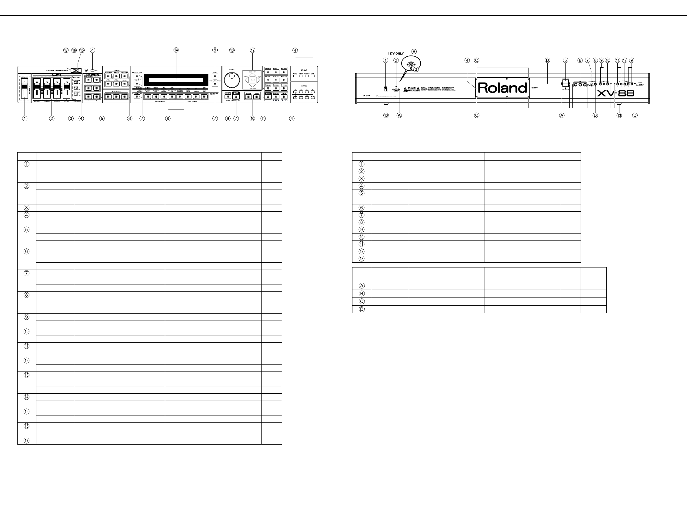
LOCATION OF CONTROLS
LOCATION OF CONTROLS PARTS LIST
No. PART CODE PART NAME DESCRIPTION Q'TY
32485261 SLIDE KNOB 248-261 1
02018790 D S-ESCT MX1H BLK L=30 1
13359366 SLIDE POTENTIOMETER EWA-NPOX05B14 10KB 1
32485261 SLIDE KNOB 248-261 4
22225366 D S-ESCUTCHEON M4H BLK 222-366 1
00891789 30M/M SLIDE POTENTIOMETER EWANPEX05B14 30MM 4
02129567 POT DUST COVER POT DUST COVER 1
01125890 D S-KEYTOP SD1H-A CLR 16
01783801 TACT SWITCH SKHJFF WITH LED AMBER 16
01783934 N S-KEYTOP MD2H 3
01787045 LED(ORANGE) SLR-325DCT31 6
01340290 TACT SWITCH EVQ11A H=5.0 6
01783945 N S-KEYTOP MD3H 3
01787045 LED(ORANGE) SLR-325DCT31 9
01340290 TACT SWITCH EVQ11A H=5.0 9
01783923 N S-KEYTOP MD1H 5
01787045 LED(ORANGE) SLR-325DCT31 5
01340290 TACT SWITCH EVQ11A H=5.0 5
01783956 N S-KEYTOP MD4H 2
01787045 LED(ORANGE) SLR-325DCT31 8
01340290 TACT SWITCH EVQ11A H=5.0 8
01783967 N S-KEYTOP MX1H 2
01340290 TACT SWITCH EVQ11A H=5.0 2
01783978 N S-KEYTOP MX2H 1
01340290 TACT SWITCH EVQ11A H=5.0 2
01783989 N S-KEYTOP MX3H BLK 4
01340290 TACT SWITCH EVQ11A H=5.0 12
01234090 D T-KEYTOP MX4B BLK 1
01340290 TACT SWITCH EVQ11A H=5.0 4
22485303 D R-KNOB L BLK 248-303 1
01905467 ROTARY ENCODER EVE GC1 F20 24B 1
02123012 ENCODER HOLDER 1
01783856 DISPLAY COVER 1
00787212 LCD UNIT (OPTLX) DMC2079NY-LA-B 1
01900623 LED TLN205 1
02230578 LED SPACER LDS-50R 1
01900612 DIODE TPS611 1
12169368 LED SPACER LDS-40B 1
01343089 ESCUTCHEON D-BEAM CONTROLLER ESCT BLK 1
/
パネル配置図
パネル配置図
パネル配置図パネル配置図
/
パネル配置図パーツリスト
パネル配置図パーツリスト
パネル配置図パーツリストパネル配置図パーツリスト
No. PART CODE PART NAME DESCRIPTION Q'TY
01784401 SEESAW SWITCH SDDJE1-A-2 10A/250VAC 1
02019112 WIRING W1 1
02019167 AC CORD ASSY (120V) UP-880-J01 1
02018878 EXP COVER 1
01780712 CARD CONECTR CN015P-3013-0 1
01343101 ESCUTCHEON D C-ESCT BX1H BLK 1
13429274 MIDI SOCKET YKF51-5041 1
01127067 SLIDE SWITCH SSSF123-P06S0 1
13429911 DIN JACK TCS7927-28-401 (RS422) 1
13449284 6.5MM JACK HLJ7001-01-3010 4
00569278 6.5MM JACK LGR4609-7100 1
13449283 6.5MM JACK HLJ7101-01-3010 2
13449258 6.5MM JACK HLJ4306-01-3080 1
12359105 RUBBER FOOT W RS-09 235-105 4
No. PART CODE PART NAME DESCRIPTION Q'ty
40011312 SCREW 3X8
40011123 SCREW 4X8
40010278 SCREW M3X12
40237101 SCREW M3X8
BINDING TAPTITE P FE BZC
BINDING TAPTITE B FE BZC
BINDING
PAN MACHINE W/SW+PW BZC
MACHINE
FE BZC
64
02
66
44
Q'ty
(for 117V)
2
Page 3
MAR, 2000 XV-88
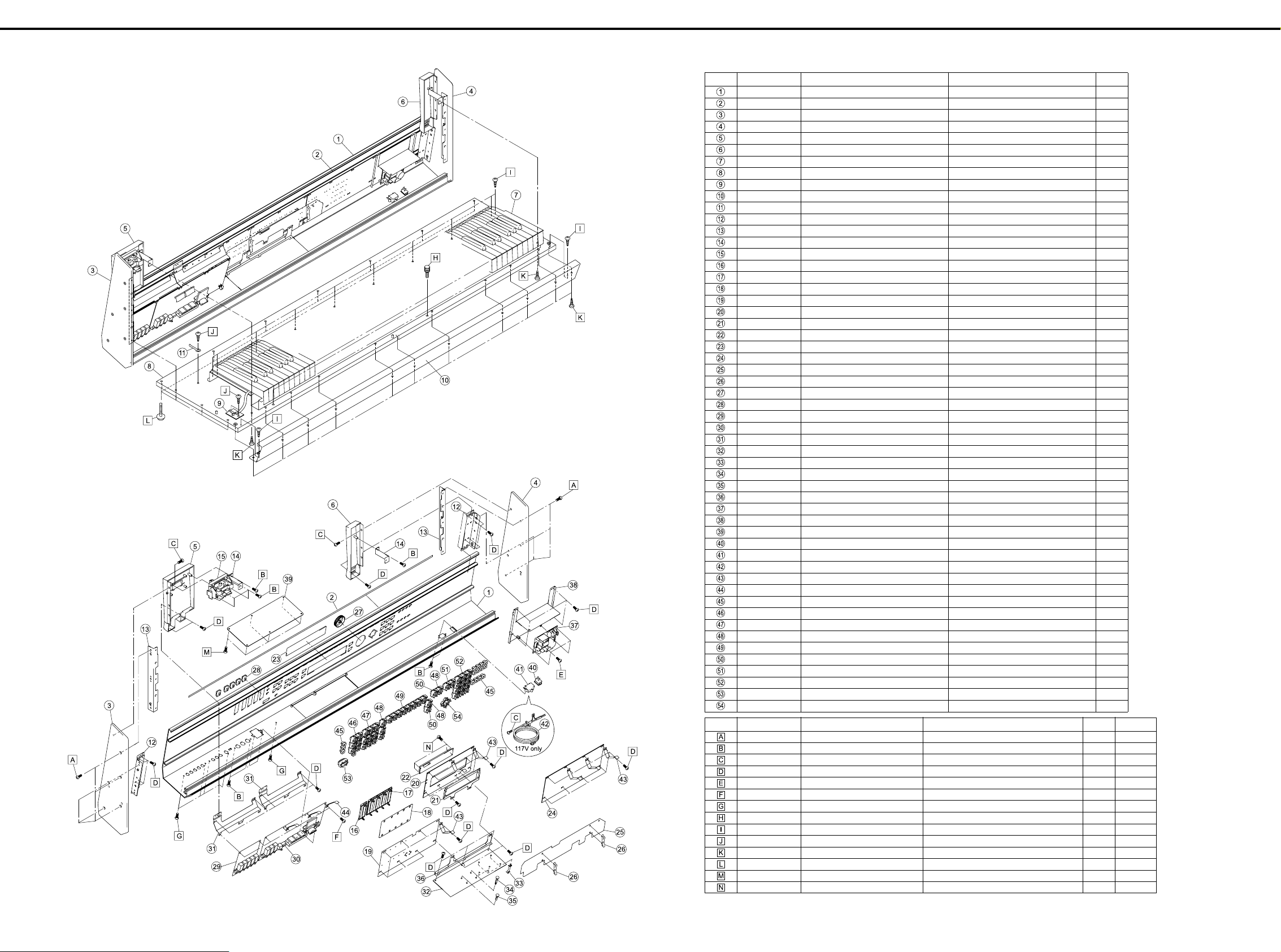
EXPLODED VIEW
/
分解図
分解図
分解図分解図
EXPLODED VIEW PARTS LIST
No. PART CODE PART NAME DESCRIPTION Q'TY
02018812 TOP PANEL 1
22265286 KEY FELT 226-286 1
02018823 SIDE PANEL L 1
02018834 SIDE PANEL R 1
02128634 END BLOCK L 1
02128645 END BLOCK R 1
71675234 PA-4A88AFT-G KEYBOARD ASSY 1
71565556 BOTTOM BOARD 1
71562178 AFT BOARD ASSY 1
02018856 BLIND 1
40017356 COATING CLIP CS-4 1
02128334 PANEL ANGLE 2
00788967 SIDE ANGLE 2
00128089 END BLOCK HOLDER 2
70564101 BENDER TURBOLESS PB-H0201 1
02018790 D S-ESCT MX1H BLK L=30 1
22225366 D S-ESCT M4H BLK 222-366 L=30 1
02129567 POT DUST COVER 1
71562112 PANEL-A KEYTOP ASSY 1
71562134 PANEL-B KEYTOP ASSY 1
02018867 DISPLAY HOLDER 1
00787212 LCD UNIT (OPTLX) DMC2079NY-LA-B 1
01783856 DISPLAY COVER 1
71562156 XV-88 PANEL-C KEYTOP ASSY 1
02231756 XV-88 INSULATING SHEET 1
02230590 CLIP CLAMP B-4S 2
22485303 D R-KNOB L BLK 248-303 1
32485261 SLIDE KNOB M BLK/LCG 5
71565534 ANALOG BOARD ASSY 1
71562201 MAIN BOARD ASSY 1
02018889 PWB HOLDER MAIN 2
71562190 EXP BASE BOARD ASSY 1
12189810 PCB SPACER WLS-14-094VO 6
02019034 PWB SPACER RSPLS-12L 2
01902756 PWB SPACER RSPS-12L 2
02018890 PWB HOLDER EXP 1
01785823 SWITCHING REGULATOR A1DU2L3B034 1
02018901 PWR SPLY HOLDER 1
02018878 EXP COVER 1
01784401 SEESAW SWITCH SDDJE1-A-2 10A/250VAC 1
02019112 WIRING W1 1
02019167 AC CORD ASSY 120V UP-880-J01 1
02235345 LEAF A 6
02235323 LEAF B 3
01125890 D S-KEYTOP SD1H-A CLR 16
01783934 N S-KEYTOP MD2H 3
01783945 N S-KEYTOP MD3H 3
01783923 N S-KEYTOP MD1H 5
01783956 N S-KEYTOP MD4H 2
01783967 N S-KEYTOP MX1H 2
01783978 N S-KEYTOP MX2H 1
01783989 N S-KEYTOP MX3H 4
01343089 ESCUTCHEON D-BEAM CONTROLLER ESCT BLK 1
01234090 D T-KEYTOP MX4B BLK 1
No. PART CODE PART NAME DESCRIPTION Q'TY
40346289 SCREW 4X12 OVAL HEAD TAPTITE B NI 10 10
40011312 SCREW 3X8 BINDING TAPTITE P FE BZC 12 10
40011123 SCREW 4X8 BINDING TAPTITE B BZC 2 4
40011067 SCREW 3X8 BINDING TAPTITE B FE ZC 48 48
40013067 SCREW M3X8 PAN MACHINE W/SW+SMALL PW ZC 4 4
40239734 SCREW 3X6 VWH TAPTITE B ZC 7 7
40237101 SCREW M3X8 PAN MACHINE W/SW+PW FE BZC 5 5
00568756 STOP SCREW (NEW TYPE) PA-4A 2 2
40012145 SCREW 4X14 TRUSS TAPPING A1 FE BZC 12 12
40010734 SCREW 3X12 BINDING TAPPING A1 FE ZC 3 3
40010134 SCREW M4X20 TRUSS MACHINE BZC 13 13
40128512 SCREW 4X25X20 VW TAPTITE B BZC 13 13
40010278 SCREW M3X12 BINDING MACHINE BZC 6 6
40344256 SCREW 3X6 PAN HEAD TAPTITE S ZC 4 4
/
分解図パーツリスト
分解図パーツリスト
分解図パーツリスト分解図パーツリスト
Q'TY
(for 117V)
3
Page 4
XV-88 MAR, 2000
PARTS LIST //// パーツリスト
SAFETY PRECAUTION:*1
The parts marked have safety-related
characteristics. Use only listed parts for
replacement.
安全上の注意:*1
が付いている部品は、安全上特別な規
格でつくられたものです。
交換の際は、指定された部品番号以外の部
品は使わないようにして下さい。
*1 *2
CASING
00788967 SIDE ANGLE 2
# 02018856 BLIND 1
01783856 DISPLAY COVER 1
# 02018878 EXP COVER 1
# 02128645 END BLOCK R 1
# 02128634 END BLOCK L 1
# 02018823 SIDE PANEL L 1
# 02018834 SIDE PANEL R 1
00568756
# 02129567 POT DUST COVER 1
# 02018790 D S-ESCT MX1H BLK L=30 1
22225366 D S-ESCUTCHEON M4H BLK 222-366 1
# 02018812 TOP PANEL 1
71565556 BOTTOM BOARD
CHASSIS
# 02128334 PANEL ANGLE 2
00128089 END BLOCK HOLDER 2
# 02018889 PWB HOLDER MAIN 2
# 02018890 PWB HOLDER EXP 1
# 02018901 PWR SPLY HOLDER 1
# 02018867 DISPLAY HOLDER 1
KNOB, BUTTON
22485303 D R-KNOB L BLK 248-303 1
32485261 SLIDE KNOB 248-261 5
01125890 D S-KEYTOP SD1H-A CLR 16
01234090 D T-KEYTOP MX4B BLK 1
SWITCH
01784401
01127067 SSSF123-P06S0 SLIDE SWITCH SW2 on Main Board 1
01340290 EVQ11A H=5.0 TACT SWITCH
01783801
JACK, EXP TERMINAL
13449284 HLJ7001-01-3010 6.5MM JACK
13449258 HLJ4306-01-3080 6.5MM JACK JK3 on Analog Board 1
13449283 HLJ7101-01-3010 6.5MM JACK JK5,JK4 on Analog Board 2
13429274 YKF51-5041 MIDI SOCKET JK1 on Main Board 1
13429911 TCS7927-28-401 (RS422) DIN JACK JK5 on Main Board 1
01780712 CN015P-3013-0 CARD CONECTR CN16 on Main Board 1
00569278 LGR4609-7100 6.5MM JACK JK2 on Main Board 1
00905234
パーツリスト
パーツリストパーツリスト
The parts marked # are
new (initial parts). *2
# の付いた部品は新規部
品です。*2
/ ケース
/ ケース
/ ケース / ケース
STOP SCREW (NEW TYPE)
/ シャーシ
/ シャーシ
/ シャーシ / シャーシ
/ つまみ、ボタン
/ つまみ、ボタン
/ つまみ、ボタン / つまみ、ボタン
/ スイッチ
/ スイッチ
/ スイッチ / スイッチ
SDDJE1-A-2 10A/250VAC
SKHJFF WITH LED AMBER
/ ジャック、外部接続端子
/ ジャック、外部接続端子
/ ジャック、外部接続端子 / ジャック、外部接続端子
ECP01-5A (PLUG FOR BRC-230T)
CONSIDERATIONS ON PARTS ORDERING
When ordering any parts listed in the parts list. please specify the following items in the order sheet.
QTY PART NUMBER DESCRIPTION MODEL NUMBER
Ex 10 22575241 S harp key C-20/50
15 2247017300 Knob (orange) DAC-15D
Failure to completely fill the above items with correct numb er and description will result in delaye d or even
undelivered replacement.
パーツ発注に関するお願い
オーダーシートには、必ず下記の4項目は正確に記入して下さい。(例外は除く)
必要数 パーツナンバー 品名 使用機種
例) 10 22575241 Sharp key C-20/50
15 2247017300 Knob (orange) DAC-15D
もし記入洩れ、誤記等が有る場合、必要部品が発送できなかったり、大幅な遅れの原因になります。御
協力をお願いします。
PA-4A 2
SEESAW SWITCH 1
SW12,SW4,SW5,SW6,SW7,SW9,SW11,SW3,SW13,SW15,
SW16,SW17,SW18,SW19,SW10 on Panel-A Board,SW23,
SW20,SW32,SW22,SW24,SW25,SW26,SW27,SW28,SW29,
SW30,SW31, SW21 on Panel-B Board,SW50,SW68,SW37,
SW38,SW39,SW42,SW44,SW51,SW52,SW58,SW65,SW43,
SW66,SW59,SW64,SW63,SW62,SW
TACT SWITCH
EURO CONVERTER PLUG 1
SW1,SW2,SW8,SW14 on Panel-A Board ,SW46,
SW47,SW33,SW34,SW35,SW36,SW56,SW45,
SW48,SW53,SW54,SW55 on Panel-C Board
JK2,JK1 on Analog Board ,JK4,JK3 on Main Board
Q'ty
15+20+13
4+12
2+2
DISPLAY UNIT
00787212 DMC2079NY-LA-B LCD UNIT (OPTLX) 1
NOTE: Replacement DMC2079NY-LA-B should be made on a unit base.
注意 : DMC2079NY-LA-B の交換は、ユニット単位で行って下さい。補修品は、ユニット単位。
POWER SUPPLY UNIT
01785823 A1DU2L3B034 SWITCHING REGULATOR 1
NOTE: Replacement A1DU2L3B034 should be made on a unit base.
注意 : A1DU2L3B034 の交換は、ユニット単位で行って下さい。補修品は、ユニット単位。
BENDER UNIT
70564101 PB-H0201 BENDER TURBOLESS 1
NOTE: Replacement PB-H0201 should be made on a unit base.
注意 : PB-H0201 の交換は、ユニット単位で行って下さい。補修品は、ユニット単位。
KEYBOARD ASSY
# 71675234
NOTE: See 'KEYBOARD PARTS LIST' for details.
注意 : 詳しくは、鍵盤パーツリストを参照してください。
PCB ASSY
# 71565534 ANALOG BOARD ASSY 1
NOTE: 'ANALOG BOARD ASSY' includes the following parts.
注意 : 補修用 ANALOG BOARD ASSY は、下記の部品を含みます。
00890567 RIBBON CABLE 11X100-P2.0 1
12199584 GROUNDING TERMINAL M1698
40342856 COATING CLIP CP-1S 1
# 71562201 MAIN BOARD ASSY (EXG) 1
NOTE: 'MAIN BOARD ASSY' includes the following parts.
注意 : 補修用 MAIN BOARD ASSY は、下記の部品を含みます。
01343101 ESCUTCHEON D C-ESCT BX1H BLK 1
12199584 GROUNDING TERMINAL M1698
40011189 SCREW M3X8 PAN TAPTITE-P FE ZC 2
40342856 COATING CLIP CP-1S 2
# 71562112 PANEL-A KEYTOP ASSY 1
NOTE: 'PANEL-A KEYTOP ASSY' includes the following parts.
注意 : 補修用 PANEL-A KEYTOP ASSY は、下記の部品を含みます。
01783934 N S-KEYTOP MD2H 3
01783945 N S-KEYTOP MD3H 3
# 02018789 WIRING
01343089 ESCUTCHEON
12169368 LED SPACER LDS-40B 1
# 02230578 LED SPACER LDS-50R 1
# 71562156 PANEL-C KEYTOP ASSY 1
NOTE: 'PANEL-C KEYTOP ASSY' includes the following parts.
注意 : 補修用 PANEL-C KEYTOP ASSY は、下記の部品を含みます。
# 01783989 N S-KEYTOP MX3H BLK 4
01783923 N S-KEYTOP MD1H 1
01783978 N S-KEYTOP MX2H 1
01783967 N S-KEYTOP MX1H 1
# 02123012 ENCODER HOLDER 1
# 71562134 PANEL-B KEYTOP ASSY 1
NOTE: 'PANEL-B KEYTOP ASSY' includes the following parts.
注意 : 補修用 PANEL-B KEYTOP ASSY は、下記の部品を含みます。
01783956 N S-KEYTOP MD4H 2
01783923 N S-KEYTOP MD1H 4
01783967 N S-KEYTOP MX1H 1
/ 表示ユニット
/ 表示ユニット
/ 表示ユニット / 表示ユニット
/ 電源ユニット
/ 電源ユニット
/ 電源ユニット / 電源ユニット
/ ベンダーユニット
/ ベンダーユニット
/ ベンダーユニット / ベンダーユニット
/ 鍵盤完成品
/ 鍵盤完成品
/ 鍵盤完成品 / 鍵盤完成品
PA-4A88AFT-G KEYBOARD ASSY
/ 基板完成品
/ 基板完成品
/ 基板完成品 / 基板完成品
10X400-P2.0-SB20-JB20-F
D-BEAM CONTROLLER ESCT BLK
TER1,TER2 on Analog Board ,TER1,TER2 on Main Board
TER1,TER2 on Analog Board ,TER1,TER2 on Main Board
CN2 on Panel-A Board 1
1
2
2
1
4
Page 5

MAR, 2000 XV-88
# 71562178 AFT BOARD ASSY 1
# 71562190 EXP BASE BOARD ASSY 1
NOTE: 'EXP BASE BOARD ASSY' includes the following parts.
注意 : 補修用 EXP BASE BOARD ASSY は、下記の部品を含みます。
12189810 PCB SPACER WLS-14-094VO 6
02019034 PWB SPACER RSPLS-12L 2
01902756 PWB SPACER RSPS-12L 2
IC
15189197 NJM5532DD IC (OP AMP)
15189251 M5218AP IC (BIPOLAR OP AMP) IC4 on Analog Board 1
# 02014389
01679978
00129278 SSC1080F0B IC IC38 on Main Board 1
01342978 TC160G22AF-1253 IC (CUSTOM) IC3 on Main Board 1
01902212
02010290 VG2618165CJ-6-EL-10 IC (DRAM) IC5 on Main Board 1
01906712 LC324260AJ-60-TLM IC (DRAM) IC21,IC20 on Main Board 2
02010023
02010056
01561945 LH28F160S5T-L70 IC (FLASH MEMORY) IC2 on Main Board 1
01451578 AK4324-VF-E2 IC (DAC) IC59,IC55 on Main Board 2
15269219H0 HD74LS05FPEL IC (TTL) IC69 on Main Board 1
15259865T0 TC74HC4053AF(TP2) IC (C MOS) IC13,IC31 on Main Board 2
15249121 TC7W04F(TE12L) IC (CMOS) IC46 on Main Board 1
15249104 TC7S04F(TE85L) IC (CMOS) IC36,IC74 on Main Board 2
15259708T0 TC74HC08AF(TP2) IC IC9,IC32 on Main Board 2
15259716T0 TC74HC32AF(TP2) IC (HS-CMOS) IC49 on Main Board 1
15259738T0 TC74HC138AF(EL) IC (CMOS) IC37 on Main Board 1
15259702T0 TC74HC02AF(EL) IC (HS-CMOS) IC22 on Main Board 1
15259758T0 TC74HC175AF(EL) IC IC47 on Main Board 1
15259809T0 TC74HC393AF(EL) IC (CMOS) IC41 on Main Board 1
15259823T0 TC74HC574AF(EL) IC (CMOS) IC40 on Main Board 1
15259884 TC7S08F(TE85L) IC (CMOS) IC66,IC61 on Main Board 2
15259887 TC7SU04F(TE85L) IC (CMOS) IC71 on Main Board 1
15259769T0 TC74HC238AF(EL) IC (CMOS) IC35 on Main Board 1
15249112 TC7W32F(TE12L) IC (CMOS) IC14 on Main Board 1
15249111 TC7WU04F(TE12L) IC (CMOS) IC19,IC39,IC8 on Main Board 3
01670789 TC74VHCT08AF IC (CMOS) IC42 on Main Board 1
00564701 TC7SH08F(TE85L) IC (CMOS) IC18 on Main Board 1
01783523 TC74VHCT245AFT(EL) IC (CMOS) IC48,IC68 on Main Board 2
02124934 TC74VHC541FTEL IC (CMOS) IC67 on Main Board 1
00670290 TC74VHC139F(EL) IC (CMOS) IC73 on Main Board 1
15289106 M5238AFP-600C IC (JFET OP AMP) IC10,IC63 on Main Board 2
15289105 UPC4570G2-E2 IC (BIPOLAR OP AMP) IC12,IC30,IC33,IC34 on Main Board 4
15289117 NJM5532MD-TE1 IC (OP AMP) IC53,IC54 on Main Board 2
01899790 UPC29L33T-E2 IC (REGULATOR) IC45 on Main Board 1
01458445 UPC29M33T-T1 IC (REGULATOR) IC9 on EXP Base Boaerd,IC15 on Main Board 1+1
15199137 AN7805F IC (V.RGL) IC52 on Main Board 1
01783534 SN7534051NS IC IC72 on Main Board 1
15289123 M51953AFP-600C IC (RESET) IC11 on Main Board 1
15289125 PC-410KT 178FAY IC (PHOTO COUPLER) IC70 on Main Board 1
15189189 UPC4570HA IC (BIPOLAR OP AMP) IC2 on Panel-A Board 1
01785012 HA17324 IC (BIPOLAR OP AMP) IC1 on Panel-A Board 1
01122267 TC74VHCT245F(EL) IC (CMOS)
00236834 TC74VHC21F(EL) IC (CMOS) IC7 on EXP Base Boaerd 1
00231889 TC74VHC32F(EL) IC (CMOS) IC6 on EXP Base Boaerd 1
00567534 TC74VHC138F(EL) IC (CMOS) IC11 on EXP Base Boaerd 1
HD6437042AA10F VER1.00
RA09-002XP6TC203C180AF002
UPD431000AGW-70LL-E2
UPD23C128040LGY-849-MJH
UPD23C128040LGY-850-MJH
IC (32BIT CPU) IC4 on Main Board 1
IC (CUSTOM) IC16,IC17 on Main Board 2
IC (SRAM) IC6,IC7 on Main Board 2
IC (MASK ROM) IC23 on Main Board 1
IC (MASK ROM) IC27 on Main Board 1
IC1,IC2,IC3 on Analog Board ,IC3 on Panel-A Board
IC4,IC10,IC5,IC3,IC2,IC1,IC8 on EXP Base Boaerd
3+1
TRANSISTOR
15129187 2SC3327-A(TPE4) TRANSISTOR Q6,Q1,Q2,Q3,Q5,Q7,Q8,Q4 on Analog Board 8
15309113 2SA1213-O(TE12R.C) TRANSISTOR Q35 on Main Board 1
00901523
01121278 2SA1576A T106 QRS TRANSISTOR Q2 on Main Board 1
15319101 2SC2412KR T146 TRANSISTOR Q33,Q32 on Main Board 2
15319114 2SC2873-Y(TE12R.C) TRANSISTOR Q30 on Main Board 1
15329533 RN2307(TE85R) TRANSISTOR Q38 on Main Board 1
01783612 RN2426(TE85L) TRANSISTOR
00239801 DTA114EU T-106 TRANSISTOR Q37 on Main Board 1
15329531 RN1308-TE85R TRANSISTOR Q39 on Main Board 1
15329521 RN1307(TE85R) TRANSISTOR Q3,Q34,Q36 on Main Board 3
01451245 RN1414(TE85L) TRANSISTOR
15119134 2SA933STPR TRANSISTOR Q2 on Panel-A Board 1
01674878 2SC5395-T12-E TRANSISTOR Q3 on Panel-A Board 1
DIODE
01017512 RB411D T146 SCHOTTKY DIODE D6,D2 on Main Board 2
02233890 DCB010-TB ARRAY DIODE on MAIN 1
01897189 MA147-(TX) ARRAY DIODE
15339130 MA142WK-(TX) ARRAY DIODE DA9 on Main Board 1
01126823 RD20S-T1 B ZENER DIODE D10,D9,D11,D8 on Main Board 4
01456456 TE-17 13B ZENER DIODE D4 on Main Board 1
# 01900612 DIODE TPS611 Q1 on Panel-A Board 1
15019126 1SS133 T-77 SWITCHING DIODE
# 01900623 LED TLN205 LED16 on Panel-A Board 1
01787045 SLR-325DCT31 LED (ORANGE)
/ ダイオード
/ ダイオード
/ ダイオード / ダイオード
RESISTOR
13749809T0 SR25TRE 332 J 1/6W CARBON RESISTOR R42,R24,R36,R18,R48,R30 on Analog Board 6
13749821T0 SR25TRE 103 J CARBON RESISTOR
13749797T0 SR25TRE 102 J CARBON RESISTOR R12,R6 on Analog Board ,R20,R17,R24 on
13749815T0 SR25TRE 562 J CARBON RESISTOR R7,R1 on Analog Board 2
13749819T0 SR25TRE 822 J 1/6W CARBON RESISTOR R20,R2,R8,R16,R27,R28,R32,R39,R40,R45,
13749793T0
13749765T0 SR25TRE 470 J CARBON RESISTOR R3,R10,R9,R4 on Analog Board 4
13749773T0 SR25TRE 101 J CARBON RESISTOR
15399708 MCR25 JZH J 470 MTL.FILM RESISTOR R117,R116,R115 on Main Board 3
00567401 RPC05T 823 J MTL.FILM RESISTOR R267 on Main Board 1
7
00567378 RPC05T 473 J MTL.FILM RESISTOR R208,R204,R100,R230 on Main Board 4
00567323 RPC05T 223 J MTL.FILM RESISTOR R83,R82 on Main Board 2
00567245 RPC05T 472 J MTL.FILM RESISTOR
15399349 RPC10T 100 J 1/10W MTL.FILM RESISTOR R140 on Main Board 1
00567345 RPC05T 333 J MTL.FILM RESISTOR R97,R102,R99,R92,R94 on Main Board 5
00567412 RPC05T 104 J MTL.FILM RESISTOR
/ トランジスター
/ トランジスター
/ トランジスター / トランジスター
2SA1681 (SC-62)(POW SW)
/ 抵抗
/ 抵抗
/ 抵抗 / 抵抗
SR25TRE 681 J 680 OHM 1/4W
TRANSISTOR Q31 on Main Board 1
Q4,Q5,Q6,Q7,Q8,Q9,Q10,Q21,Q11 on Main Board
Q15,Q18,Q13,Q14,Q17,Q16,Q12 on Main Board
DA5,DA10,DA19,DA18,DA15,DA13,DA3,DA11,
DA8,DA7,DA6,DA4,DA2,DA1,DA12 on Main Board
D1,D13,D10,D46,D22,D21,D20,D19,D18,D17,D16,
D15,D11,D12,D2,D9,D7,D6,D5,D3,D4,D8,D14 on
Panel-A Board,D32,D23,D24,D25,D26,D27,D28,
D29,D31,D33,D34,D35,D30 on Panel-B Board
D38,D43,D49,D48,D45,D51,D44,D50,D42,D41,
D39,D71,D37,D36,D52,D40,D64,D70,D68,
D67,D69,D65,D53,D62,D61,D60,D59,D58,D57,
D56,D54,D66 on Panel-C Board
LED8,LED15,LED14,LED13,LED12,LED11,LED9,
LED7,LED5,LED3,LED2,LED1,LED6,LED10, LED4
on Panel-A Board,LED22,LED17,LED18,LED19,
LED21,LED24,LED25,LED26,LED27,LED28,LED23,
LED20 on Panel-B Board, LED29 on Panel-C Board
R41,R47,R5,R17,R11,R35,R31,R29,R23,R19 on
Analog Board ,R26,R22,R15,R7 on Panel-A Board
Panel-A Board
R46,R15 on Analog Board
CARBON RESISTOR R25,R21,R13,R37,R33,R43 on Analog Board 6
R22,R34,R44,R14,R38,R26 on Analog Board,
R3,R23,R19,R14,R4,R2,R1,R11 on Panel-A Board
R241,R273,R256,R37,R250,R258,R44 on Main Board
R245,R212,R98,R233,R93,R91,R45 on Main Board
15
23+32+13
15+1 +12
10+4
2+3
12
6+8
9
7
7
7
5
Page 6

XV-88 MAR, 2000
00567289 RPC05T 103 J MTL.FILM RESISTOR
00567390 RPC05T 683 J MTL.FILM RESISTOR R104 on Main Board 1
00567556 RPC05T 105 J MTL.FILM RESISTOR R60,R48,R19,R111 on Main Board 4
15399373 RPC10T 101 J 1/10W MTL.FILM RESISTOR R200,R198 on Main Board 2
15399381 RPC10T 221 J 1/10W MTL.FILM RESISTOR R195 on Main Board 1
15399411 RPC10T 392 J 1/10W MTL.FILM RESISTOR R145,R191,R182,R153,R144,R187,R154,
15399421 RPC10T 103 J 1/10W MTL.FILM RESISTOR
15399397 RPC10T 102 J 1/10W MTL.FILM RESISTOR R203 on Main Board 1
15399425 RPC10T 153 J MTL.FILM RESISTOR R143,R186,R185,R177,R156,R152,R194,
15399445 RPC10T 104 J 1/10W MTL.FILM RESISTOR R197 on Main Board 1
15399401 RPC10T 152 J 1/10W MTL.FILM RESISTOR R201 on Main Board 1
01011856 RPC05T 0R0 J MTL.FILM RESIST0R C525,R57,C526,C512,R131,R124,R114,R73,
00567212 RPC05T 332 J MTL.FILM RESISTOR R127,R17 on Main Board 2
15399709 MCR25 JZH J 680 1/4W MTL.FILM RESISTOR R121,R118,R120,R119 on Main Board 4
00567156 RPC05T 102 J MTL.FILM RESISTOR R231,R110,R109,R43 on Main Board 4
00567112 RPC05T 471 J MTL.FILM RESISTOR R270,R246,R234,R20 on Main Board 4
00567078 RPC05T 271 J MTL.FILM RESISTOR R62,R113,R232,R244 on Main Board 4
00567067 RPC05T 221 J MTL.FILM RESISTOR R236,R237,R238,R16,R235 on Main Board 5
00567023 RPC05T 101 J MTL.FILM RESISTOR R49,R74,R269,R75,R76,R272,R53,R77,R239,
00566967 RPC05T 470 J MTL.FILM RESISTOR R30,R61,R63,R265,R266 on Main Board 5
00566934 RPC05T 330 J MTL.FILM RESISTOR R271 on Main Board 1
00566867 RPC05T 100 J MTL.FILM RESISTOR R35,R106,R105,R95,R67,R66 on Main Board 6
00567034 RPC05T 121 J MTL.FILM RESISTOR R240 on Main Board 1
00567267 RPC05T 682 J MTL.FILM RESISTOR R210,R126 on Main Board 2
00567423 RPC05T 124 J MTL.FILM RESISTOR R268 on Main Board 1
00567301 RPC05T 153 J MTL.FILM RESISTOR R255 on Main Board 1
00566912 RPC05T 220 J MTL.FILM RESISTOR R249 on Main Board 1
00908389 MCR100JZH J 331 MTL.FILM RESISTOR R199,R202,R207,R205 on Main Board 4
01010445 EXBV8V331JV R-ARREY(330) RA63,RA61 on Main Board 2
15409113 EXBV8V103JV RESISTOR ARRAY
01013578 EXBV8V470JV RESISTOR ARRAY RA19,RA17 on Main Board 2
00126112 EXBV8V101JV RESISTOR ARRAY RA57,RA51,RA50,RA13,RA11 on Main Board 5
01457145 EXBE10C103J RESISTOR ARRAY RA21,RA1,RA16,RA25,RA26,RA28,RA68,
01013923 EXBV8V100JV RESISTOR ARRAY RA37,RA40,RA66,RA38,RA34,RA36,RA35,
00126101 EXBV8V221JV RESISTOR ARRAY RA22 on Main Board 1
# 02019023 EXBE10C682J RESISTOR-ARRAY RA59,RA62,RA64 on Main Board 3
01457156 EXBE10C332J RESISTER ARRAY RA60 on Main Board 1
# 13749863T0 SR25TRE 564 J CARBON RESISTOR R8 on Panel-A Board 1
13749845T0 SR25TRE 104 J 1/4W CARBON RESISTOR R28 on Panel-A Board 1
13749833T0 SR25TRE 333 J CARBON RESISTOR R10 on Panel-A Board 1
13749805T0 SR25TRE 222 J CARBON RESISTOR R12 on Panel-A Board 1
13749791T0 SR25TRE 561 J CARBON RESISTOR R18 on Panel-A Board 1
13749781T0 SR25TRE 221 J CARBON RESISTOR R6 on Panel-A Board 1
13749779T0 SR25TRE 181 J CARBON RESISTOR R16 on Panel-A Board 1
13749190 SR50TR 100 J CARBON RESISTOR "R27,R5 on Panel-A Board 2
13749799T0 SR25TR 122J RESISTOR R13 on Panel-A Board 1
13749837T0 SR25TRE 473 J CARBON RESISTOR R9 on Panel-A Board 1
15399301 RPC10T 0R0 J MTL.FILM RESISTOR R1,R2 on EXP Base Boaerd 2
02013489 MNR35J5RJ103 RESISTOR ARRAY
15399917 MNR34J5ABJ103 RESISTOR ARRAY RA24 on EXP Base Boaerd 1
R247,R28,R27,R26,R36,R209,R40,R254,R253,
R252,R251,R248,R135,R23,R107,R133,R132,
R129,R108,R31,R257,R243,R81,R80,R79,R78,
R58,R55,R41,R259,R6,R242,R211,R2,R3,R5,
R7,R9,R10,R22,R15,R4 on Main Board
R178 on Main Board
R9,R7 on EXP Base Boaerd,R196 on Main Board
R148 on Main Board
R72,R71,R69,R68,R206,R64,R8,R47,R11,R24,
R25,R65,R29 on Main Board
R90,R96,R101,R112,R125 on Main Board
RA9,RA52,RA43,RA42,RA39,RA53 on Main Board
RA2,RA27 on Main Board
RA41,RA65,RA58,RA56,RA46,RA45,RA44,
RA18,RA20,RA29,RA30,RA31,RA32,RA33,
RA47 on Main Board
RA10,RA7,RA5,RA1,RA26,RA12 on EXP Base Boaerd
42
2+1
21
14
22
POTENTIOMETER / ボリューム
13359366 EWA-NPOX05B14 10KB
00891789 EWANPEX05B14 30MM
CAPACITOR / コンデンサー
13519534 50VK 1000PF CAPACITOR
13519641 DD308-959F104Z50 CERAMIC CAPACITOR C44,C48,C57,C3,C38,C34,C33,C28,C24,C21,
8
00239412 AMZV0050J122 0200 POLYEST. CAPACITOR C14,C52,C42,C26 on Analog Board 4
00239390 AMZV0050J561 0200 POLYEST. CAPACITOR C19,C31,C56,C47 on Analog Board 4
01900823 RA2-16V100M-T2 CHEMICAL CAPACITOR
8
01900834 RA2-16V101M-T2 CHEMICAL CAPACITOR
01675367 GRM39CH471J50PT CERAMIC CAPACITOR C31 on Main Board 1
01674190 ECUV1H150JCV CERAMIC CAPACITOR C210,C198-203,C205-209,C223,C224,C226,
01674701
15359707R0
# 00567889 GRM39B332K50PT CERAMIC CAPACITOR C218,C211,C212,C213,C214,C215,C216,
01349312 GRM39F105Z10PT CERAMIC CAPACITOR C347,C345,C60 on Main Board 3
01675278 GRM39CH101J50PT CERAMIC CAPACITOR C370,C63 on Main Board 2
00567945 GRM39B103K50PT CERAMIC CAPACITOR
6
9
00566856 GRM39SL681J50PT CERAMIC CAPACITOR C59 on Main Board 1
00567834 GRM39B122K50PT CERAMIC CAPACITOR C64 on Main Board 1
01672423 GRM40CH101J50PT CERAMIC CAPACITOR C340 on Main Board 1
01454889
00341901 16MV470HC CHEMICAL CAPACITOR C339 on Main Board 1
01893656 ROS-16V101M-T2 CHEMICAL CAPACITOR C330,C334 on Main Board 2
02124923 RV3-25V470MZ7-R CHEMICAL CAPACITOR C328 on Main Board 1
01783467 RV2-16V101MZ7-R CHEMICAL CAPACITOR
01783489 RV2-16V470MZ7-R CHEMICAL CAPACITOR C194,C3,C13,C75,C102,C134 on Main Board 6
01564778
# 02018701 DD104-989SL680J50 CERAMIC CAPACITOR C33,C28 on Panel-A Board 2
13529132 RPE132-901F104Z50
# 02018690 R2A-16V101M-T2 CHEMICAL CAPACITOR C15,C13 on Panel-A Board 2
13639546M0 ECEA1CKA100B 10UF/16V CHEMICAL CAPACITOR C21,C16 on Panel-A Board 2
15359206R0 GRM40F104Z25PT10 CERAMIC CAPACITOR
ECJ1VF1E104Z 0.1UF/16VK
GRM40F104Z50PT85 0.1UF/50V
RA2-16V470MT2 470UF/16V
RV2-16V100MZ7-R 10UF/16V
INDUCTOR, COIL, FILTER / インダクター、コイル、フィルター
6
12449355 FBR07HA850TB00 TAPE INDUCTOR L19,L18,L21,L15,L11,L2,L22,L12,L5,L6 on
00903167 N2012Z601T02 (CHIP) FERRITE-BEAD L1-L25 on Main Board 25
/ ボリューム
/ ボリューム / ボリューム
/ コンデンサー
/ コンデンサー / コンデンサー
/ インダクター、コイル、フィルター
/ インダクター、コイル、フィルター / インダクター、コイル、フィルター
POTENTIOMETER(SLIDE)
POTENTIOMETER (SLIDE)
CERAMIC CAPACITOR C108,C99,C110,C68,C112-119,C57,C248,
CERAMIC CAPACITOR C269,C261,C260,C287,C277,C282,C338,
CHEMICAL CAPACITOR C336,C332 on Main Board 2
CHEMICAL CAPACITOR
MLT.LAY.CERAMIC CAPACITOR
VR5 on Panel-A Board 1
VR4,VR3,VR2,VR1 on Panel-A Board 4
C39,C7,C11,C18,C30,C46,C54,C25 on Analog Board
C17,C13,C40,C6,C9 on Analog Board
C16,C23,C27,C37,C43,C12,C5,C2 on Analog Board,
C270,C271,C306,C307,C259 on Main Board
C45,C15,C53,C4,C41,C10,C22,C29,C35,
C36 on Analog Board ,C266,C264 on Main Board,
C32,C30,C7,C3 on Panel-A Board
C229,C235-238,C233,C231,C33-C42,C197,
C43,C196,C121,C120,C46,C45 on Main Board
C253,C119,C125,C109,C82,C92,C93,C94,C90
C85-89,C100,C83,C81,C80,C78,C77,C72,
C71,C95,C96,C97,C70,C98,C84,C195,C179,
C52,C180,C55,C48,C30,C181,C29,C27,C178,
C193,C49,C204,C221,C239,C242,C245,C91,
C249,C24,C250,C251,C252
C249,C24,C250,C251,C252,C184,C132,C127,
C128,C32,C130,C168,C133,C138,C147,C150,
C152,C154,C167,C157,C161,C162,C129,C164,
C165,C156 on Main Board
C337,C335,C305,C333,C291,C314,C317,
C319,C325,C329,C331 on Main Board
C217 on Main Board
C158,C159,C169,C182,C183,C365,C153 on Main Board
C11 on EXP Base Boaerd,C323,C322 on Main Board
C29,C35,C34,C32,C3,C2 on EXP Base Boaerd,
C131,C18,C151,C243,C247,C124,C246,C25,
C26,C50,C56,C76,C79 on Main Board
C20,C14,C8,C25,C9,C10,C11,C27,C31,C12,
C29 on Panel-A Board
C17,C26,C23,C22,C19,C18,C27,C14,C13,C28,
C10,C37,C9,C6,C5,C4,C1,C12,C31,C36,C38,C39,
C40,C41,C42,C33,C30 on EXP Base Boaerd
Analog Board
15
8+5
10+2+4
39
150
18
1+2
6+13
11
27
8
8
7
9
6
Page 7
MAR, 2000 XV-88
CRYSTAL, RESONATOR / クリスタル、発振子
00901912 MA-406 24.576MHZ TE24 CRYSTAL X2 on Main Board 1
01893790 MA-406 8.25MHZ CRYSTAL X1 on Main Board 1
01340745 MA-406 12MHZ CRYSTAL X3 on Main Board 1
ENCODER / エンコーダー
01905467 EVE GC1 F20 24B ROTARY ENCODER EN1 on Panel-C Board 1
CONNECTOR / コネクター
13429300 51048-1100(11P) CABLE HOLDER CN2 on Analog Board 1
# 02129623 SB20-10WS FOR PCB CONNECTOR CN1 on Analog Board 1
# 02014445 CONNECTOR 20FE-BT-VK-N CN11 on Main Board 1
02019012 26FE-BT-VK-N CONNECTOR CN14 on Main Board 1
01908645 16FE-BT-VK-N CONNECTOR CN13 on Main Board 1
01908634 14FE-BT-VK-N CONNECTOR CN12 on Main Board 1
02018990 34FE-BT-VK-N CONNECTOR CN1 on EXP Base Boaerd,CN5 on Main Board 1 +1
# 02019001
# 02129723
13369598 52147-0310 3PIN WIRE TRAP CN5 on AFT Board ,CN15 on Main Board 1 +1
13369606 52147-1110(11P) WIRE TRAP CN18 on Main Board 1
13369926 53253-0410 (2MM PITCH) CONNECTOR CN10 on Main Board 1
13369592 B7B-XH-A(7P) JST CONNECTOR CN19 on Main Board 1
# 02018689 32FE-ST-VK-N FOR PCB CONNECTOR CN1 on Panel-A Board 1
# 02018723 26FE-ST-VK-N FOR PCB CONNECTOR CN6 on Panel-C Board 1
# 02018712
13439311 520314-2 CONNECTOR CN4 on AFT Board 1
13429833 52411-0402 40P CONNECTOR CN5,CN6 on EXP Base Boaerd 2
02010078 TX25-80P-6ST-E1 CONNECTOR CN3,CN4 on EXP Base Boaerd 2
WIRING, CABLE / ワイヤリング、ケーブル
# 02019112 WIRING W1
# 02019090 WIRING 4X600-P2.0-51065-51065-F 1
# 02019101 WIRING 7X1200-P2.5-XHP-XHP-F 1
# 02019089 WIRING 15X400-P2.0-SB20-51065-F 1
01014867 RIBON CABLE 3X650-P2.0 1
# 02231689 BAN CARD BNCD-P=1.25-K-34-320 1
# 02231678 BAN CARD BNCD-P=1.25-K-32-400 1
# 02231712 BAN CARD BNCD-P=1.25-K-26-550 1
# 02231701 BAN CARD BNCD-P=1.25-K-20-450 1
# 02231690 BAN CARD BNCD-P=1.25-K-32-160 1
/ エンコーダー
/ エンコーダー / エンコーダー
/ コネクター
/ コネクター / コネクター
32FE-BT-VK-N FOR WIRING
SB20-15WS FOR PCB 2MM PITCH
20FE-ST-VK-N FOR WIRING
/ ワイヤリング、ケーブル
/ ワイヤリング、ケーブル / ワイヤリング、ケーブル
/ クリスタル、発振子
/ クリスタル、発振子 / クリスタル、発振子
CONNECTOR
CONNECTOR CN1 on Main Board 1
CONNECTOR CN3 on Panel-B Board 1
CN2 on EXP Base Boaerd,CN9,CN6 on Main Board
1 +2
1+1+1+1
PACKING / 梱包材
# 02129578 LOWER PAD CNTR 1
# 02018923 UPPER PAD L 1
# 02018945 UPPER PAD R 1
# 02018956 LOWER PAD 2
# 02018989 UPPER PAD CNTR 1
# 02018912 PACKING CASE 1
MISCELLANEOUS / その他
12569249 LITHIUM BATTERY CR2032 220MAH/3V 1
40128534 DOUBLE FACED
40122612 NITTO ACETATE TAPE #5 BLACK W10MM 30M 20P
# 02230590 CLIP CLAMP B-4S 2
# 02235323 LEAF B 3
# 02235345 LEAF A 6
# 02231756 INSULATING SHEET INSULATING 1
40017356 COATING CLIP CS-4 1
40016512 INSULOK TIE 80M/M T-18S 1
12189815 BATTERY HOLDER BH-32 BT1 on Main Board 1
# 40122889 DOUBLE-FACED TAPE #501 W10MM 20M 20P(CM) 2
22265286 KEY FELT 226-286 1
00569156 CUSHION T1X25X1200 1
12359105 RUBBER FOOT W RS-09 235-105 4
# 40231845 STRAIGHT PIN 6X20 FOR WOOD 3
ACCESSORIES (STANDARD) / 標準付属品
# 02019167 AC CORD ASSY 120V UP-880-J01 1
13499219 AC CORD SET (100V) DC-382-J01 VFF2P 1
13499221 AC CORD SET (230V) EC-511-E07 H03VVH2-F 2P 1 +1
13499222 AC CORD SET (240VA) SC-078-J02 ES206-75HMA 1
# 71565912 OWNER'S MANUAL JAPANESE 1
# 71565945 OWNER'S MANUAL ENGLISH 1
40232334
/ 梱包材
/ 梱包材 / 梱包材
/ その他
/ その他 / その他
ADHESHIVE TAPE
保証書
#575X W30MM 30M (CM) 10
/ 標準付属品
/ 標準付属品 / 標準付属品
JAPAN ONLY 1
15+120
SCREW / ねじ類
40011312 SCREW 3X8
40010278 SCREW M3X12 BINDING MACHINE BZC 6
40010134 SCREW M4X20 TRUSS MACHINE BZC 13
40010734 SCREW M3X12
40012145 SCREW M4X14
40128512 SCREW 4X25X20
# 40346289 SCREW 4X12 OVAL HEAD TAPTITE B NI 10
40011067 SCREW 3X8 BINDING TAPTITE B FE ZC 24+24
40011123 SCREW M4X8 BINDING TAPTITE B BZC 2 +2
40239734 SCREW 3X6 PAN VWH TAPTITE B ZC 7
40013067 SCREW M3X8
40237101 SCREW M3X8
# 40344256 SCREW 3X6
40010745 SCREW M3X16
40011734 NUT M4X11.5
40019434 NUT M5X12
/ ねじ類
/ ねじ類 / ねじ類
BINDING TAPTITE P FE BZC
BINDING HEAD TAPPING A1 FE ZC
TRUSS TAPPING A1 FE BZC
PAN WASHER HEAD TAPTITE B BZC
PAN MACHINE W/SW+SMALL PW ZC
PAN MACHINE W/SW+PW FE BZC
PAN HAEAD TAPTITES FE BZC
BINDING HEAD TAPPING A1 FEZC
ANCHOR B FOR WOOD BZC
ANCHOR B FOR WOOD BZC
2+10+2+2+2
12
13
3
4
5
4
4
2
2
7
Page 8
XV-88 MAR, 2000
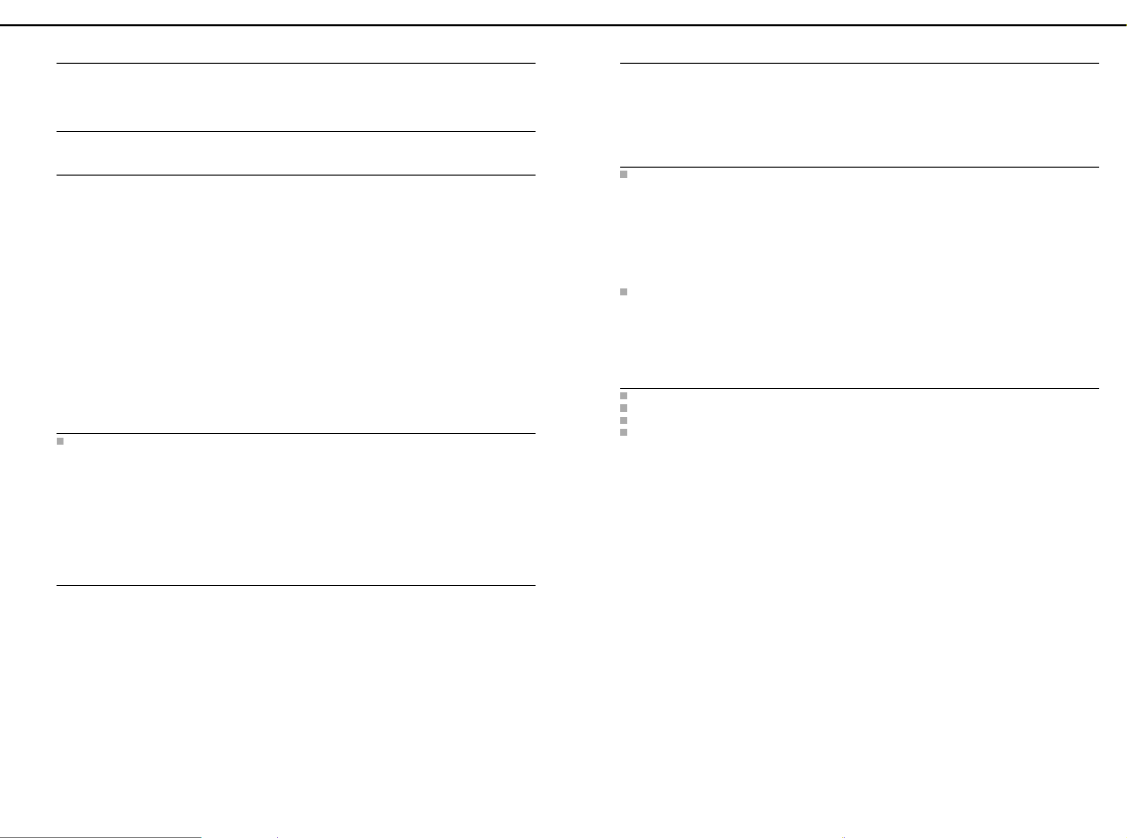
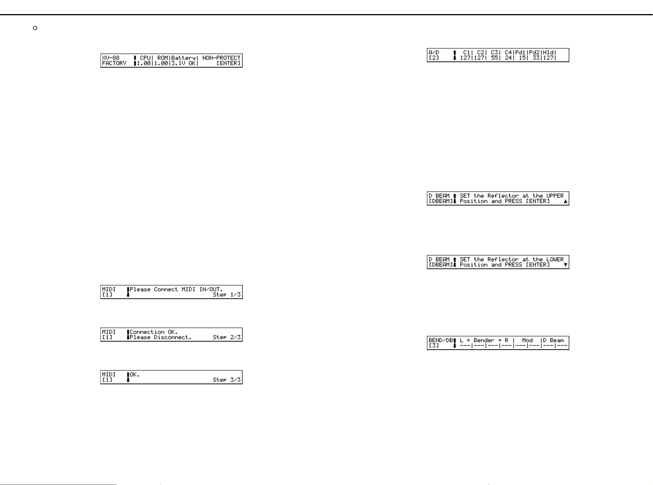
IDENTIFYING THE VERSION NUMBER
1. Turn on the power while pressing [EXIT].
2. Pressing [UNDO/COMP] key while the opening message is displayed
enables TEST MODE where the Top page appears.
The version numbers of the CPU and ROM will appear on the display.
*fig_ver1
USER DATA SAVE AND LOAD
Using the SmartMedia
* Before beginning the operation, format the SmartMedia.
• Formatting Procedure
1.
With the XV-88 power off, insert the SmartMedia in the memory card slot.
2. Turn on the XV-88 power.
3. Press [UTILITY].
4. Use the [ ] cursor key to show the "UTIL2" screen.
fig_svld1.eps
バージョンナンバーの確認方法
バージョンナンバーの確認方法
バージョンナンバーの確認方法バージョンナンバーの確認方法
1. [EXIT] を押しながら電源を入れます。
2. オープニング・メッセージ表示中に [UNDO/COMP] を押すと、テスト
モードに入りトップ・ページになります。
ここで、CPU,ROM それぞれのバージョンが表示されます。
ユーザーデータのセーブとロード
ユーザーデータのセーブとロード
ユーザーデータのセーブとロードユーザーデータのセーブとロード
◯
スマートメディアを使用する場合
スマートメディアを使用する場合
スマートメディアを使用する場合スマートメディアを使用する場合
※ 作業を開始する前に、スマートメディアのフォーマットを行ってください。
・・・・ フォーマットの方法
フォーマットの方法
フォーマットの方法フォーマットの方法
1. 電源を切った状態で、スマートメディアをメモリーカードスロットに
挿し込みます。
2. 電源を入れます。
3. [UTILITY] を押します。
4. カーソルキー [ ↓ ] で「UTIL2」の画面にします。
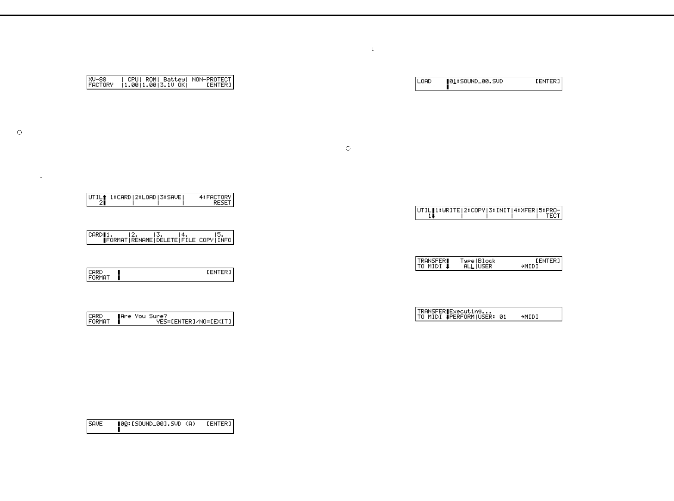
• Loading the User Data
1. Check that the SmartMedia is inserted in the memory card slot.
2. Press [UTILITY].
3. Press the [ ] cursor key to show the "UTIL2" screen. Select "LOAD"
with the cursor keys and press [ENTER] to show the following screen.
fig_svld6.eps
4. Confirm the file name to be loaded and press [ENTER] to perform data
loading.
If more than one file are written on the SmartMedia, press [INC/+] or
[DEC/-] to select the object file name and then perform loading.
Bulk Dump Procedure
Items Required:
MIDI cable
•
Sequencer (Recordable)
•
• Saving the User Data
1.
Connect the MIDI OUT terminal of the XV-88 to MIDI IN with a MIDI cable.
2. Press [UTILITY].
fig_svld7.eps
・・・・ ユーザーデータのロード
ユーザーデータのロード
ユーザーデータのロードユーザーデータのロード
1. スマートメディアがメモリーカードスロットに挿し込まれていることを
確認します。
2. [UTILITY] を押します。
3. カーソルキー [ ↓ ] を押して「UTIL2」の画面にします。
カーソルキーで「2:LOAD」を選び、[ENTER] を押すと、以下のような画
面を表示します。
4. ロードするファイル名を確認し、[ENTER] を押すと、データロード が行
われます。
スマートメディアに複数のファイルが書き込まれてい る場合、[INC/+]
[DEC/-] を押して、目的のファイル名を選んでからロードを行ってください。
◯
バルクダンプで行う場合
バルクダンプで行う場合
バルクダンプで行う場合バルクダンプで行う場合
< 準備するもの >
・MIDI ケーブル
・シーケンサー(録音可能なもの)
・・・・ ユーザーデータのセーブ
ユーザーデータのセーブ
ユーザーデータのセーブユーザーデータのセーブ
1. XV-88 の MIDI OUT と , シーケンサーの MIDI IN を MIDI ケーブルで接
続します。
2. [UTILITY] を押します。
5. Select "1:CARD" with the cursor keys and press [ENTER].
fig_svld2.eps
6. Select "1.FORMAT" with the cursor keys and press [ENTER].
fig_svld3.eps
7. Press [ENTER], and the display will show the following screen. Pressing [ENTER] again allows formatting to be performed.
fig_svld4.eps
8. When the formatting ends, the display will return to showing the screen
in step 6 Pressing [EXIT] causes the format screen to disappear.
* Before removing the SmartMedia from the slot, turn off the XV-88
power.
• Saving the User Data
*fig_svld5
5. カーソルキーで「1:CARD」を選び、[ENTER] を押します。
6. カーソルキーで「1.FORMAT」を選び、[ENTER] を押します。
7. [ENTER] を押すと、以下のような画面になり、さらに [ENTER] を押す
と、フォーマットが実行されます。
8. フォーマットが終わると、4. の画面に戻ります。[ENTER] で 6. の
画面に行き、[EXIT] でフォーマット画面を抜けます。
※ スマートメディアをスロットから取り出すときは、電源を切ってから
行ってください。
・・・・ ユーザーデータのセーブ
ユーザーデータのセーブ
ユーザーデータのセーブユーザーデータのセーブ
1. スマートメディアがメモリーカードスロットに挿し込まれていること
を確認します。
2. [UTILITY] を押します。
3. カーソルキー [ ↓ ] を押して「UTIL2」の画面にします。
4. カーソルキーで「3:SAVE」を選び、[ENTER] を押します。
3. Press the cursor key to select "4:XFER" and press [ENTER].
4. The display wull be show "TRANSFER TO MIDI" screen and set the setting to Type = All, Block = USER.
fig_svld8.eps
5. Begin recording with the sequencer.
6. Press [ENTER] to begin the transfer of data. When the data begins to be
sent correctly, the display will show the following screen.
fig_svld9.eps
7. When the transmission ends, the display will show the message "COMPLETE" and automatically return to showing the screen in step 4.
• Loading the User Data
1. Connect the MIDI IN terminal of the XV-88 to the MIDI OUT terminal of
the sequencer with a MIDI cable.
2. Send the bulk dump from the sequencer.
3. カーソルキーを押して「4:XFER」を選び、[ENTER] を押します。
4. TRANSFER TO MIDI の設定を Type = All、Block = USER に設定します。
5. シーケンサーの録音を開始します。
6. [ENTER] を押して、データの転送を開始します。正しくデータが送 られ
始めると以下の画面を表示します。
7. 送信が終わると、「COMPLETE」の表示が出て、自動的に元の画面に戻り
ます。
・・・・ ユーザーデータのロード
ユーザーデータのロード
ユーザーデータのロードユーザーデータのロード
1. XV-88 の MIDI IN と、シーケンサーの MIDI OUT 端子をケーブルでつな
げます。
2. シーケンサーからバルクダンプを送信します。
5. さらに [ENTER] を押すとデータセーブが行われます。
※ スマートメディアに、すでに同名のファイルが書き込まれているとき
には、上書きをして良いかを聞いてきます。元のファイルを保存して
おきたいときには、カーソルキーを用いて新たなファイル名を入力し
てからセーブを行ってください。
8
Page 9
MAR, 2000 XV-88
FACTORY RESET
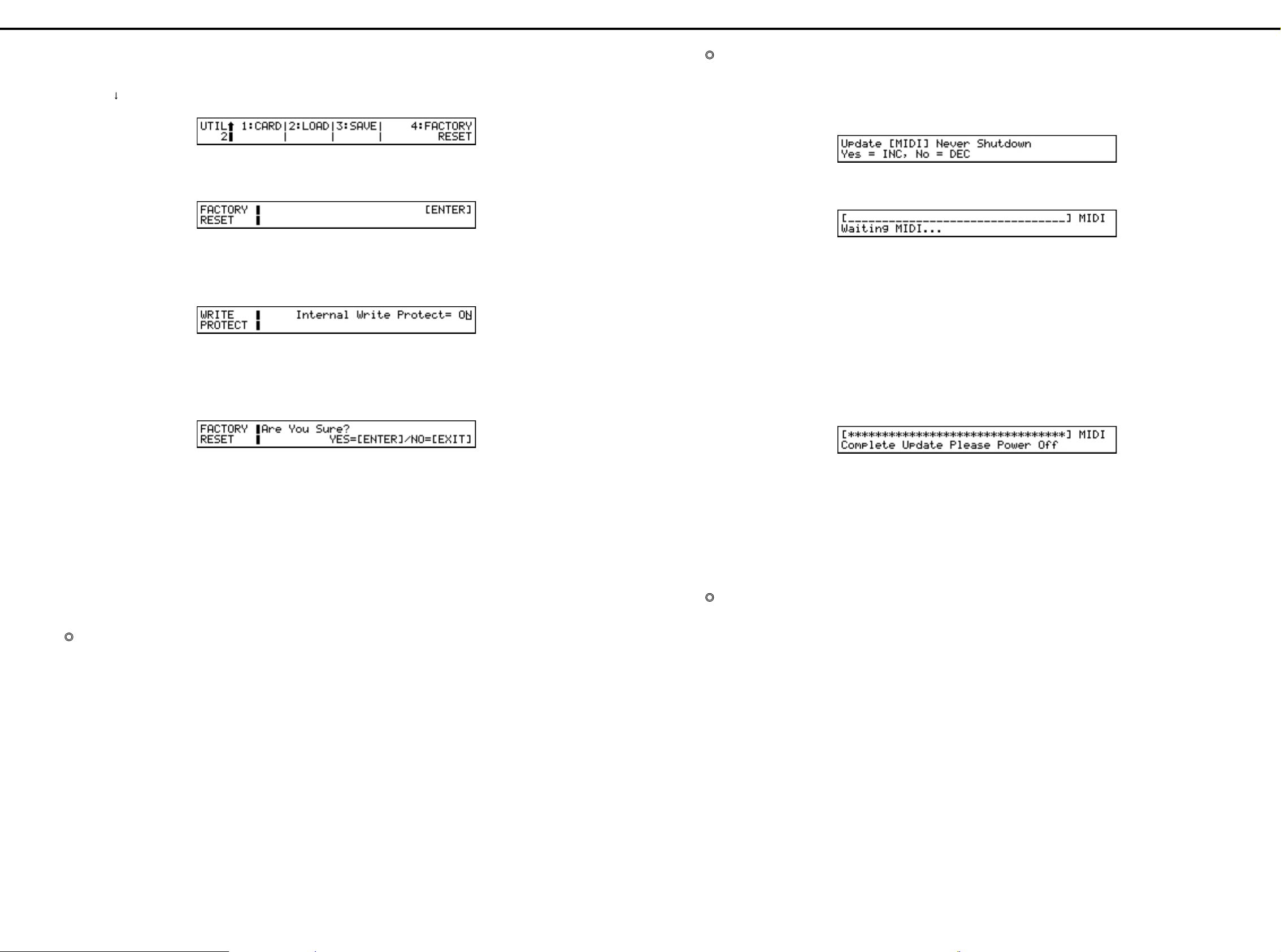
1. Press [UTILITY].
2. Press the [ ] cursor key to show the "UTIL2" screen.
fig_fact1.eps
3. Select "4:FACTORY RESET" with the cursor keys, then press [ENTER],
and the display will show the following screen.
fig_fact2.eps
4. Press [ENTER].
If Internal Write Protect is ON, a warning will be issued and then the
•
display will show the following screen.
fig_fact3.eps
Press [DEC/-] to turn Internal Write Protect OFF, then press [ENTER],
and the display will return to showing the screen in step 3.
If Internal Write Protect is OFF, the display will show the following
•
screen.
fig_fact4.eps
ファクトリーリセットの方法
ファクトリーリセットの方法
ファクトリーリセットの方法ファクトリーリセットの方法
1. [UTILITY] を押します。
2. カーソルキー [ ↓ ] を押して、「UTIL2」の画面にします。
3. カーソルキーで「4:FACTORY RESET」を選び、[ENTER] を押すと、以下の
ような画面になります。
4. [ENTER] を押します。
・ Internal Write Protect が ON の場合、警告の後、以下の画面が表
示されます。
[DEC/-] を押して Internal Write Protect を OFF にしてから [ENTER] を
押すと、3 の画面に戻ります。
Å@
・ Internal Write Protect が OFF の場合は、以下の画面になります。
Version Up Procedure
1. Connect the MIDI cable from MIDI OUT of the external sequencer to
MIDI IN of the XV-88.
2. Turn on the XV-88 power while holding down [DEC/-] and [A] at the
same time, and the display will show the following MIDI update screen.
fig_update1.eps
3. Press [INC/+], and the display will show the following screen, waiting
for the reception of MIDI data.
fig_update2.eps
4. After confirming the display in step 3, regenerate all the "..mid" files in
the XV-88 Ver. Up Disks 1 and 2 from the external sequencer (the
order does not matter). During the reception of MIDI data, the "MIDI
message" LED blinks and the message "Waiting" changes to the message "Receiv-ing."
When the data transfer of one file ends, the message "Waiting" will
appear on the display. Then regenerate the next file.
The use of a sequencer with a chain play function, such as the XP-80,
allows the version to be upgraded even more easily. Load and play the
".svc" file (chain file), and all the ".mid" files found on Disk 1 will be
auto-matically regenerated. When regenerating Disk 1 all ends,
replace with Disk 2 and play it again.
5. When the update ends normally, the display will show the following
screen and the [A] to [H] LED's will blink.
fig_update3.eps
◎◎◎◎
バージョンアップの方法
バージョンアップの方法
バージョンアップの方法バージョンアップの方法
1. MIDI ケーブルを外部シーケンサーの MIDI OUT から XV-88 の MIDI
IN に接続します。
シーケンサーで SMF をチェインプレイできるように設定します。
2. [DEC/-] と [A] を同時に押しながら電源を入れると、以下のような
MIDI アップデート画面に入ります。
[INC/+] を押すと次の表示になり、MIDI データの受信待ち状態になります。
3.
4. 3. の表示を確認した後、XV-88 Ver.Up Disk 1,2 の中にある全ての
".mid" ファイルを外部シーケンサから再生します。(順序は問いませ
ん)MIDI データ受信中は [MIDI message] の LED が点滅し、
「Waiting」の表示が「Recieving」に変わります。1 つのファイルの
データ転送が終了すると、表示が「Waiting」になりますので、続け
て次のファイルを再生して下さい。
なお、XP-80 等のチェインプレイ機能を持つシーケンサーを用いる
と、より簡単にバージョンアップができます。Disk 1 の中にある
".svc" ファイル(チェインファイル)をロードし、PLAY すると 、
Disk 1の中の全ての ".mid" ファイルを自動的に再生します。Disk 1
の再生が全て終了したら、Disk 2 に入れ替えて再び PLAY します。
5. アップデートが正常に終了すると次の表示になり、[A] -- [H] の
LED が点滅します。
Factory reset is performed when [ENTER] is pressed.
VERSION UP
The XV-88 uses a flash memory for the program ROM. The version of the
program ROM can be upgraded by loading MIDI data into the XV-88.
After upgrading the version, factory reset must be performed. If important
data is written in the user memory, save the data on a card before
upgrading the version.
Required Items
XV-88 Ver. Up Disk (2DD: Two disks) (#17048530)
•
Sequencer capable of regenerating SMF (Also possible using a syn-
•
thesizer with a sequencer)
MIDI cable
•
[ENTER] を押すとファクトリーリセットが実行されます。
フラッシュ ROM のバージョンアップの方法
フラッシュ ROM のバージョンアップの方法
フラッシュ ROM のバージョンアップの方法フラッシュ ROM のバージョンアップの方法
XV-88 は、プログラム ROM にフラッシュメモリを使用しています。
これらは外部から MIDI データを送り込むことによりバージョンアップ
できます。なお、バージョンアップ後は必ずファクトリーリセットを行
う必要があります。ユーザーメモリに大切なデータが書込まれている場
合は、データを保存(「ユーザーデータのセーブとロード」参照)して
からバージョンアップ作業を行なって下さい。
◎◎◎◎
用意するもの
用意するもの
用意するもの用意するもの
・ XV-88 Ver.Up Disk (2DD:2 枚組)(#17048530)
・ SMF の再生できるシーケンサー (XP-80 等のシーケンサー付きシンセ
サイザーでも可)
・ MIDI ケーブル
6. After playing all the ".mid" files on the two Ver. Up Disks, turn off the
XV-88 power to exit VERSION UP.
7. Lastly, perform test mode. (See page 10.)
Be sure to test the following test items
Top page (Identifying the version number)
•
D Beam Adjustment
•
Bender/D Beam Test
•
Factory Reset
•
This completes the version up.
NOTES:
Number of SMF's
One SMF is created for one block of flash memory.
•
Thirty-two SMF's, p00001.mid to p00032.mid, are created.
•
Some files may be omitted depending on the size of the program.
•
SMF is always created in p00032.mid because checksum data is
•
placed in it.
Ending the update
When p00032.mid has been received, it is judged that all the update
•
data has been received.
Any block, which has not been updated at this point of time, will be
•
erased.
This is performed to properly control the checksum data in the exter-
•
nal ROM.
Therefore, some blocks only cannot be updated.
•
6. 2 枚の Ver.Up Disk の全ての ".mid" ファイルをプレイし終わったら、
電源を切りアップデートを終了します。
7. 最後にテストモードを行います。(P10 参照)以下の項目は必ず行っ
て下さい。
・ TOP Page(ROM のバージョンの確認を行います。)
・ D Beam Adjustment
・ Bender/D BEAM Test
・ Factry Reset
以上でバージョンアップは終了です。
◎◎◎◎
注意点
注意点
注意点注意点
SMF の数について
SMF の数について
SMF の数について SMF の数について
・ SMF は Flash Memory の1 ブロックに対して、一つ作られます。
・ p00001.mid -- p00032.mid の 32 個の SMF が作られます。
プログラムのサイズによっては、途中のファイルが抜ける事があります。
・
・
p00032.mid にはチェックサムデータが置かれますので必ず作られます。
アップデートの終了について
アップデートの終了について
アップデートの終了について アップデートの終了について
・ p00032.mid を受信し終えると、全アップデートデータを受信した
と判断しています。
・ この時点でアップデートされなかったブロックは消去します。
・ これは外 ROM のチェックサムデータを正しく管理するためです。
・ 従って一部のブロックのみをアップデートすることはできません。
9
Page 10
XV-88 MAR, 2000
TEST MODE
Items required
Audio cable 1 through 4 pieces
•
MIDI Cable 1 piece
•
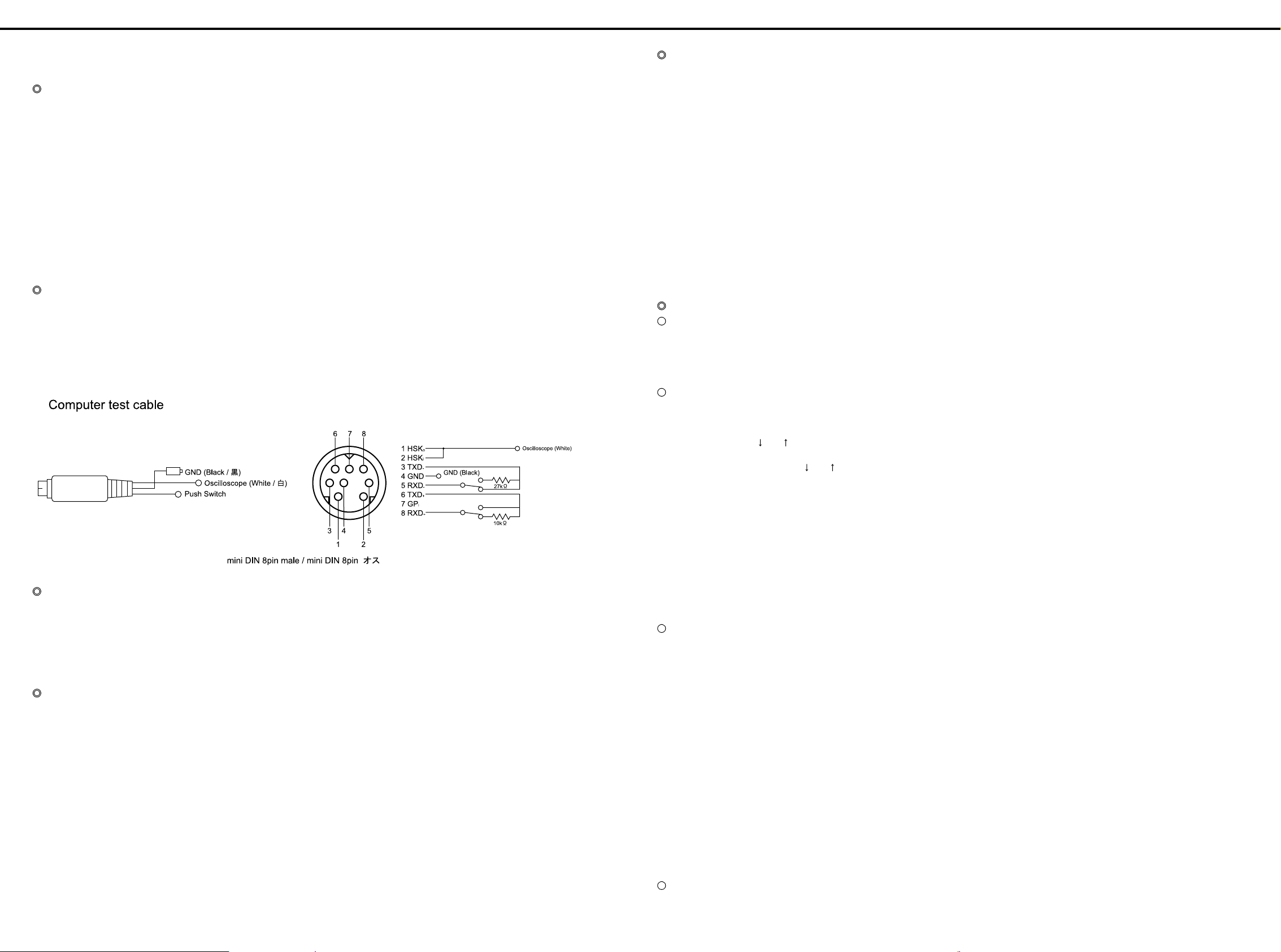
Computer test cable (#17049906) 1 piece
•
SmartMedia 2 pieces
•
(Formatted, and protected and unprotected respectively)
Expression pedal
•
Monitor speaker (MA-12 etc.)
•
Head phone
•
Oscilloscope
•
D beam adjustment jig (plate of approximately 18 cm square)
•
40 centimeters measurable scale
•
Wave expansion board SR-JV80 series 2 pieces
•
Wave expansion board SRX Series 2 pieces
•
Computer test cable
"Computer test cable" (17049906) is required to perform Computer I/F
Test in TEST MODE.
3rd pin and 5th pin, and 6th pin and 8th pins of this cable which are
male mini DIN 8 pins are connected respectively. 1st pin outputs the
waveform, and 4th pin is used as GND.
When this component is needed, please give your order to the Roland
service center.
*fig_test1
D beam adjustment jig (plate of approximately 18 cm square)
This jig is needed to perform D beam adjustment in TEST MODE. The
plate must meet the following requirements.
1. Dimensions:18 X 18 centimeters (tolerance: ± 1 centimeter)
2. Thickness: Not specified
2. Color:
3. Material: Not specified (paper is acceptable.)
Precautionary notes
User data may be erased when entering TEST MODE.
•
Be sure to make backup data.
Do not insert or eject the SmartMedia with power supply turned on,
•
or the SmartMedia may be damaged.
Be sure to turn off the power supply before inserting or ejecting the
SmartMedia.
The contents of SmartMedia are lost when card test it performed.
•
Use the SmartMedia for test when performing the card test.
Install the wave expansion board on the unit before turning on the
•
power supply.
The board may be damaged if it is installed with the power supply
turned on.
Set the computer slide switch on the rear to "MAC" before turning on
•
the power supply.
If the switch is not at this position, the computer interface cannot be
tested correctly.
Grey (non-lustrous) some characters written are acceptable.
テストモード
テストモード
テストモードテストモード
◎準備するもの
◎準備するもの
◎準備するもの◎準備するもの
・ オーディオケーブル 1~4 本
・ MIDI ケーブル 1 本
・ コンピューターテストケーブル(#17049906)1本
・ スマートメディア 2 枚
(フォーマット済みのもので プロテクトされているもの、プロテク
トされていないもの 各 1 枚ずつ)
・ エクスプレッションペダル
・ モニタースピーカー (MA-12 etc.)
・ ヘッドフォン
・ オシロスコープ
・ D ビーム調整治具 ( 約 18cm 四方の板)
・ 40 センチが計れるメジャー
・ ウェーブエクスパンションボード SR-JV80 シリーズ 2 枚
・ ウェーブエクスパンションボード SRX シリーズ 2 枚
◎コンピュータテストケーブルについて
◎コンピュータテストケーブルについて
◎コンピュータテストケーブルについて◎コンピュータテストケーブルについて
テストモードで Computer I/F Test を行う際には、"Computer test
cable"(17049906) が必要です。
これは、mini DIN 8pin オスの 3 ピンと 5 ピン、6 ピンと 8 ピンがそ
れぞれショートされ、1 ピンから波形を出力し、4 ピンから GND をと
る構造になっています。
必要な場合には、ローランドサービスセンターまでオーダーしてください。
◎ D ビーム調整治具 ( 約 18cm 四方の板)
◎ D ビーム調整治具 ( 約 18cm 四方の板)
◎ D ビーム調整治具 ( 約 18cm 四方の板)◎ D ビーム調整治具 ( 約 18cm 四方の板)
テストモードで D ビーム調整を行う際に必要です。板の条件は、以下
の通りです。
1. 大きさ:
2. 厚さ : 特に指定はありません。
2. 色 :グレー(光沢がない物)多少文字などが記載されていても
3. 材質 : 指定は、ありません(紙でも可)
◎テストを始める前の注意
◎テストを始める前の注意
◎テストを始める前の注意◎テストを始める前の注意
・ テストモードに入るとユーザーデータは消去される場合がありま
・電源を入れたまま スマートメディアの抜き差しを行うと、スマー
・ カードテストを行うと、スマートメディアの内容は失われてしま
・ ウェーブエクスパンションボードは電源を入れる前にあらかじめ
・電源を入れる前にリア面のコンピュータのスライドスイッチを Mac
18 センチ× 18 センチ(± 1センチぐらいは、問題ありません)
可。
す。必ずデータのバックアップを行って下さい。
トメディアが壊れる可能性があります。抜き差しの際は必ず電源
を切って下さい。
います。テスト用のスマートメディアを準備し、使用して下さい。
本体に装着して下さい。電源を入れたまま装着すると、ボードが
壊れる可能性があります。
にしておきます。この状態でないと コンピューター・インター
フェース のテストが正しく行われません。
Tes t it e ms
XV-88 provides the following test.
For the details of individual test, refer to their respective sections.
0 : Top Page
(Identifying the version number, Battery check, and Memory card check)
1:MIDI Test
2:A/D Test
3 : D Beam Adjustment
4 : Bender / D Beam Test
5:After touch Test
6 : Switch & LED Test
7 : LCD & Encoder Test
8 : Computer I/F Test
9 : Card Test
10: Sound Test 1
11: Sound Test 2
12: Memory Test
13: Expansion Board Test
14: Factory Reset
Operations of keys
How to enter TEST MODE
Confirm that the computer slide switch on the rear is at "MAC".
•
Turn on the power while pressing [EXIT].
•
Pressing [UNDO/COMP] key while the opening message is displayed
•
enables TEST MODE where the Top page appears.
Changing test item
Pressing [ENTER] on the top page changes the test item to "1. MIDI Test".
•
For test items 1 through 8, successful ending of individual test
•
changes the item to next one automatically.
Pressing a cursor key [ ] or [ ] during a test can change the item to
•
the next one or previous one even if the test is not completed.
* For "6. Switch & LED test", press [ ] or [ ] key while pressing
[SHIFT] key..
Pressing [EXIT] key returns the item to top page in a TEST MODE.
•
* For "6. Switch & LED test", Pressing [EXIT] while pressing [SHIFT]
returns the item to top page.
When the tests are completed consecutively from the top page and
•
"11. Sound Test 2" is completed, memories are checked automatically
in the items 12 and 13.
* When all the tests are performed successfully, the step moves to
"14. Factory Reset".
For the details of the display, refer to the description of test items in the
latter part of this document.
Jumping to another test item
Pressing a key such as a numerical key while pressing and holding
[SHIFT] selects a test item corresponding to the number directly as
described below.
0 : [SHIFT]+[EXIT] Top Page
1 : [SHIFT]+[1] MIDI Test
2 : [SHIFT]+[2] A/D Test
3 : [SHIFT]+[D BEAM] D Beam Adjustment
4 : [SHIFT]+[3] Bender / D BEAM Test
5 : [SHIFT]+[4] After touch Test
6 : [SHIFT]+[5] Switch & LED Test
7 : [SHIFT]+[6] LCD & Encoder Test
8 : [SHIFT]+[7] Computer I/F Test
9 : [SHIFT]+[CARD] Card Test
10 : [SHIFT]+[8] Sound Test 1
11 : [SHIFT]+[9] Sound Test 2
12 : * [SHIFT]+[USER] Memory Test
13 : * [SHIFT]+[EXP] Expansion Board Test
14 : [SHIFT]+[PATCH FINDER] Factory Reset
* When the test items are selected consecutively from the top page, the
memory test of items 12 and 13 are not performed automatically at the
completion of "11. Sound Test 2".
How to exit TEST MODE
Return to the top page and press [EXIT] key.
◎テスト項目
◎テスト項目
◎テスト項目◎テスト項目
XV-88 には以下のテストがあります。
各テストの詳細については、それぞれの項目を参照して下さい。
0 : Top Page
1:MIDI Test
2:A/D Test
3 : D Beam Adjustment
4 : Bender / D Beam Test
5 : Aftertouch Test
6 : Switch&LED Test
7 : LCD&Encoder Test
8 : Computer I/F Test
9 : Card Test
10: Sound Test 1
11: Sound Test 2
12: Memory Test
13: Expansion Board Test
14: Factory Reset
◎ボタン操作
◎ボタン操作
◎ボタン操作◎ボタン操作
○ テストモードへの入り方
・リア面のコンピュータのスライドスイッチを Mac にしておきます。
・ [EXIT] を押しながら電源を入れます
・ オープニング・メッセージ表示中に [UNDO/COMP] を押すと、テス
ト・モードに入りトップ・ページを表示します。
○各テスト項目の移動
・ トップ・ページで [ENTER] を押すと、テスト項目 1.MIDI TEST に移
ります。
・ テスト項目 1~8 は 各テストが正常に終了すると、自動的に次のテ
スト項目に移ります。
・カーソル [ ↓ ]/[ ↑ ] を押すと、テストが終了していなくても 次の
テスト項目 / 一つ前のテスト項目 に移動します。
※ 6.Switch&LED test では [SHIFT] と [ ↓ ] または [ ↑ ] の2つ
・ 各テストモードで [EXIT] を押すとトップページになります。
※ 6.Switch&LED Test では、[SHIFT][EXIT] の 2 つのボタンを押す
・ トップページから順にテストモードを進め 11.Sound Test 2 を終了
すると、12,13 の各種メモリチェックが自動的に行われます。
※ チェックで NG がない場合は、14.Factory Reset に移ります。
画面表示の詳細は、後述の テスト項目詳細 を参照して下さい。
○各テストへのジャンプ
[SHIFT] を押しながら テン・キー 等を押すと対応するテスト項目を直
接選択できます。
0 : [SHIFT]+[EXIT] Top Page
1 : [SHIFT]+[1] MIDI Test
2 : [SHIFT]+[2] A/D Test
3 : [SHIFT]+[D BEAM] D Beam Adjustment
4 : [SHIFT]+[3] Bender / D BEAM Test
5 : [SHIFT]+[4] Aftertouch Test
6 : [SHIFT]+[5] Switch&LED Test
7 : [SHIFT]+[6] LCD&Encoder Test
8 : [SHIFT]+[7] Computer I/F Test
9 : [SHIFT]+[CARD] Card Test
10 : [SHIFT]+[8] Sound Test 1
11 : [SHIFT]+[9] Sound Test 2
12 : * [SHIFT]+[USER] Memory Test
13 : * [SHIFT]+[EXP] Expansion Board Test
14 : [SHIFT]+[PATCH FINDER] Factory Reset
* トップページからこの方法でテスト項目を選択した場合、12,13 の各
種メモリーのテストは、11.Sound Test 2 の終了時、自動的に行われ
ません。
○ テストモードからの抜け方
トップページに戻り [EXIT] を押します。
(Identifying the version number,Battery check,Memory card check)
のボタンを押します。
とテスト・モードのトップ・ページに戻ります。
10
Page 11
MAR, 2000 XV-88
When the test is completed successfully, the test item moves to the
Details of test items
0 : Test mode top page
(Identifying the version number, Battery check, and Memory card check)
*fig_test2
◎テスト項目詳細
◎テスト項目詳細
◎テスト項目詳細◎テスト項目詳細
0 : Test mode top page
(Identifying the version number,Battery check,Memory card check)
•
next one automatically.
2 : A/D Test
*fig_test6
・ テストが正常に終了すると、自動的に次のテスト項目に移ります。
2 : A/D Test
Confirm versions of CPU and Program ROM.
•
If any version is found to be improper, perform version-up.
For the method of update, refer to "How to version-up".
Confirm the voltage of SRAM battery.
•
Battery: OK meaning that the voltage is normal.
NG meaning that the voltage is abnormal.
In case of "NG", check BT1, IC10, and Battery on the main board.
* Battery is "OK" when the voltage is in the range from 2.5 Volts to 4.0
Volts.
Confirm the state of memory card slot and the SmartMedia inserted
•
into it.
NONE SmartMedia is not inserted yet.
PROTECTED The SmartMedia is protected.
NON-PROTECT The SmartMedia is not protected.
Replace the SmartMedia and confirm all of the above three states.
•
Note: Be sure to turn off the power supply before replacing the Smart-
Media. After turning on the power supply, enter the TEST MODE
again.
In case the display is incorrect, check CN16, IC42, IC46, Q21, and
R131 through 133 on the main board.
Note:
After this, when performing the tests consecutively in the TEST
MODE, insert the card that is formatted and unprotected, and enter
the TEST MODE. "9. Card test" is to be performed in this state.
Turn Encoder to confirm that the contrast of LCD can be adjusted.
•
In case the contrast cannot be adjusted, check IC3 and IC10 on the
main board.
Press [ENTER] key to proceed to the test.
•
1 : MIDI Test
*fig_test3
Connect MIDI IN and MIDI OUT with MIDI Cable.
•
Confirm that "Connection OK" appears.
*fig_test4
・ CPU, Program ROM のバージョンを確認します。
バージョンが適切でない場合は、バージョンアップを行って下さい。
アップデートの方法については、「バージョンアップの方法」を参照
して下さい。
・ SRAM 用 バッテリー の電圧を確認します
Battery: OK 電圧正常
NG 電圧異常
NG の場合はメインボードの BT1,IC10,Battery をチェックしてくださ
い。
※ バッテリー電圧が 2.5V ~ 4.0V の場合 OK になります。
・ メモリーカードスロットと挿入したスマートメディアの状態を確認
します。
NONE スマートメディアが挿入されていません。
PROTECTED スマートメディアはプロテクトされています。
NON-PROTECT スマートメディアはプロテクトされていません。
・ スマートメディアを入れ替えて、以上の3つ全ての状態を確認して
下さい。
注:入れ替えは必ず電源を切って行い、電源投入後、再度テスト
モードに入って下さい。
表示が正しくない場合は、メインボードの CN16,IC42,IC46,Q21,
R131~133 をチェックして下さい。
注:この後、テストモードを順に行う場合は、フォーマット済みの
プロテクトされていないカードを挿入した状態でテストモード
を進んで下さい。9. Card test の項目はこの状態で行います。
・ Encoder を回すと LCD コントラストの調整ができることを確認しま
す。
調整ができない場合はメインボードの IC3,IC10 をチェックします。
・ [ENTER] を押すと、テストに移ります。
1 : MIDI Test
・ MIDI IN と MIDI OUT を MIDI ケーブルで接続します。
"Ccnnection OK" が表示されることを確認します。
Check sliders C1, C2, C3, and C4.
•
Fully move the sliders C1, C2, C3, and C4 up and down individually.
Check pedals Pd1, Pd2, and Hld.
•
Connect the expression pedal to the pedal jack.
Step on the expression pedal to return it to the home position.
* Repeat the above procedure for three pedals respectively.
Confirm that the value changes in the range from "0" to "127" for
individual pedals.
"OK" appears when the maximum value is "127" and minimum value is "0".
In case "OK" does not appear in any of the above tests, check the
following components as appropriate.
C1, C2, C3, and C4:VR1 through 4, IC1 and CN1 on the panel A board, and
Pd1,2 : JK3, JK4 ,IC31 ,IC34 and RA11 on the main board.
Hld : JK2, Q38, Q39, IC12, IC13 and RA13 on the main board.
When "OK" appears on all of the above checks, the test item moves
•
to the next one automatically.
3 : D Beam Adjustment
*fig_test7
Adjustment of D beam is performed here.
•
With this adjustment, two points, 40 cm and 5 cm, are set to place
the D BEAM control in the optimum state.
First, press [ENTER] key while holding D beam adjustment jig (18
•
cm square plate) at 40 cm position above D beam. For reference, 40
cm is approximately equivalent to 17 white keys.
*fig_test8
Then, press [ENTER] key while holding D beam adjustment jig (18
•
cm square plate) at 5 cm position above D beam. For reference, 5
cm is approximately equivalent to two white keys.
"NG" appears if these two points are not set correctly.
•
Press [ENTER] key to return to the setting screen, where the setting
can be made again.
When the adjustments are completed, the test item moves to the
•
next one automatically.
4 : Bender / D BEAM Test
*fig_test9
IC31, IC33, RA11, RA57 and CN9 on the main board.
・ C1,C2,C3,C4 :スライダー チェック
C1~C4 のスライダーを上下いっぱいに動かします。
・ Pd1,Pd2,Hld :ペダル チェック
エクスプレッション・ペダルをペダル・ジャックに挿します。
エクスプレッション・ペダルを踏んで戻します。
※ ペダル・ジャックは3つあるので、適宜接続し直してチェック
を行って下さい。
それぞれの 0 ~127 の間で変化することを確認します。
最大値が127、最小値が 0 であれば、"OK" が表示されます。
OK の表示が出ない場合、その箇所によって以下のところをチェッ
クして下さい。
C1~C4 :パネル A ボードの VR1~4,IC1,CN1, メインボードの
IC31,IC33,RA11,RA57,CN9
Pd1,2 :メインボードの JK3,JK4,IC31,IC34,RA11
Hld :メインボードの JK2,Q38,Q39,IC12,IC13,RA13
・全て"OK" となると、自動的に次のテスト項目に移ります。
3 : D Beam Adjustment
・ ここでは D ビームの調整を行います。
この調整によって 40cm と 5cm の2点を設定し、D BEAM コント
ロールを最適な状態にします。
・ 始めに、D ビームの上 40cm の位置に、D ビーム調整治具 (18cm 角
の正方形の板 ) をかざし [ENTER] を押します。なお、40cm の目安
として白鍵17 個分です。
・ 続いて、D ビームの上 5cm の位置に D ビーム調整治具 (18cm 角の
正方形の板 ) をかざし [ENTER] を押します。なお、5cm の目安とし
て白鍵 2 個分です。
・ 2つの設定が正しく行われないと、NG の画面になります。
[ENTER] を押すと設定の画面に戻るので、再度設定をして下さい。
・ 調整が終了すると、自動的に次のテスト項目になります。
4 : Bender/ D BEAM Test
Disconnect MIDI Cable from MIDI IN and MIDI OUT.
•
Confirm that "OK" appears.
*fig_test5
In case the display is not correct, check JK1, IC69, IC70 and Q37 on the
main board.
・ MIDI IN と MIDI OUT から MIDI ケーブルを抜きます。
OK の表示が出ることを確認します。
表示が正しくない場合は、メインボードの JK1,IC69,IC70,Q37 をチェッ
クして下さい。
When entering this screen, confirm that the bender is not lying.
•
(for reading the A/D value as mid-point voltage when entering this
screen)
Hold D beam adjustment jig (18 cm square plate) above the D beam
•
and move it between the 5 cm and 40 cm points.
Lay the bender lever fully to the right and left.
•
Lay the bender lever fully to the modulation side and return it.
•
The display shows as follows from the left.
Maximum value when bender is laid to the left.
Value when bender is returned from the left.
Value when bender is returned from the right.
Maximum value when bender is laid to the right.
Value when modulation is returned.
Maximum value of modulation
Minimum value of D Beam
Maximum value of D Beam
・この画面に入る時、ベンダー が倒れていないことを確認しておきま
す。( この画面に入る時の A/D 値を中点電圧として読むため )
・ D ビームの上に、D ビーム調整治具 (18cm 角の正方形の板 ) をかざ
し、5cm から 40cm の間を上下させます。
・ ベンダー・レバーを左右いっぱいに倒します。
・ ベンダー・レバーをモジュレーション側いっぱいに倒して戻しま
す。
表示は左から順に、以下のようになっています。
ベンダー L 方向最大の値
ベンダー L 方向から戻した時の値
ベンダー R 方向から戻した時の値
ベンダー R 方向最大の値
モジュレーションを戻した時の値
モジュレーションの最大の値
D Beam の最小の値
D Beam の最大の値
11
Page 12

XV-88 MAR, 2000
Confirm that the display becomes as described above.
•
*fig_test10
In case the display is not as described above, check the following components as appropriate.
D beam :
Modulation and bender
When the display is normal, the test item moves to the next one
•
automatically.
5 : After touch Test
*fig_test11
The keyboard (PA-4) of XV-88 has the following three key ranges.
•
L : Low range A0-G2 (PA-4 Low Assy)
M : Mid range A2-E5 (PA-4 Mid Assy)
H : High range F5-C8 (PA-4 Hi Assy)
Press individual three key ranges deeply and return to the home positions.
•
"OK" appears when the maximum value is "127" and minimum value is "0".
If "OK" does not appear, check CN4 and CN5 on the AFT board,
and CN15, IC12, IC13, IC34 and RA13 on the main board.
When the display is normal, the test item moves to the next one automatically.
•
6 : Switch & LED Test
*fig_test12
Confirm that all LED are lit.
•
For switches without LED, confirm that their names appear on the display.
•
Pressing a switch with LED turns off the LED.
•
Pressing a switch without LED turns off the name on the display.
•
"Beep" is heard when every time the LED or the name goes out.
•
Note: Pressing two or more switches simultaneously is ineffective.
The number of switches that are not pressed appears on the right
•
lower area of the display.
In case an LED does not go on or go off, or the content of display is
correct, check LED, SW, DA, CN1, CN3 and CN6 on the panel
board, and IC32, IC35, IC36, IC40,RA56, RA58 ,RA60 through 63,
CN9, CN11 and CN14 on the main board.
When all the switches are pressed, the test item moves to the next
•
one automatically.
7 : LCD & Encoder Test
*fig_test13
Turn Encoder to confirm that the contrast of LCD can be adjusted.
•
Confirm that the number of LEDs of PART switch changes according the value of contrast of LCD.
Press [ENTER] (first time) to confirm that all dots of LCD go off.
•
*fig_test14
Q1, Q2, Q3, LED16 and CN1 on the panel A board
CN9, IC63, IC74, RA13 and Q36 on the main board
: IC10, CN10 and bender unit on the main board
・ 表示が以下のようになることを確認します。
このようにならない場合、その箇所によって以下の箇所をチェックし
て下さい。
D ビーム : パネル A ボードの Q1,Q2,Q3,LED16,CN1 メインボードの
モジュレーション , ベンダー : メインボードの IC10,CN10, ベン
・全てOK ならば自動的に次のテスト項目になります。
5 : Aftertouch Test
・ XV-88 の鍵盤 (PA-4) は、3 つのキー・レンジがあります。
L :低音域 A0-G2 (PA-4 Low Assy)
M :中音域 A2-E5 (PA-4 Mid Assy)
H :高音域 F5-C8 (PA-4 Hi Assy)
・ 3 つのキー・レンジのそれぞれの鍵を深く押し込み、戻します。
最大値が127、最小値が 0 であれば、"OK" が表示されます。
OK の表示が出ない場合、AFT ボードの CN4,CN5, メインボードの
CN15,IC12,IC13,IC34,RA13 をチェックして下さい。
・全てOK ならば、自動的に次のテスト項目になります。
6 : Switch&LED Test
・すべての LED が点灯していることを確認します。
・ LED のないスイッチは、ディスプレイに名前が表示されていること
を確認します。
・ スイッチを押していくと LED が消灯します。
・ LED のないスイッチを押すと表示している名前が消えます。
・ 個数が減る時に BEEP 音が「ピッ」となります。
注:複数のスイッチを同時に押した場合は無効です。
・まだ押されていないスイッチの個数が右下に表示されます。
LED が点灯、消灯しない、ディスプレイの表示が正しくない場合、
パネルボードの各 LED,SW,DA,CN1,CN3,CN6, メインボードの
IC32,IC35,IC36,IC40,RA56,RA58,RA60 ~ 63,CN9,CN11,CN14 を
チェックして下さい。
全てのスイッチが押された時点で、自動的に次のテスト項目に移ります。
・
7 : LCD&Encoder Test
・ Encoder を回すと LCD コ ントラ スト が調整 でき るこ とを確認します。
LCD コントラストの値に応じて PART SW の LED 点灯個数が変化す
ることを確認します。
・
[ENTER](1回目)を押すと LCD の全ドットが消灯することを確認します。
CN9,IC63,IC74,RA13,Q36
ダーユニット
Press [ENTER] (third time) to move to the next test time.
•
8 : Computer I/F Test
*fig_test16
This test cannot be performed normally if the slide switch is not set to
•
"Mac" before the test.
In case not, turn off the power supply, set the switch to "Mac", and
then enter TEST MODE after turning on the power supply again.
Connect Computer test cable (17049906) to confirm that "Connect"
•
appears.
Disconnecting Computer test cable causes "OK" to appear.
•
In case "OK" does not appear, check JK5, IC71 and IC72 on the main
board.
Moving the slide switch to the positions of "Mac", "PC" and "MIDI" in
•
this order, the display changes as "Mac", "PC" and "MIDI".
In case the display is incorrect, check JK5, IC71 and IC72 on the main
board.
When "OK" appears and the displays with the slide switch are correct,
•
the test item moves to the next one automatically.
9 : Card Test
*fig_test17
Before performing this test, it is necessary to insert the formatted and
•
unprotected SmartMedia, or the read/write test cannot be performed.
When inserting the SmartMedia at this time, turn off the power supply,
insert the SmartMedia, and then enter TEST MODE again.
Note: The SmartMedia may be damaged if it is inserted or ejected with
the power supply turned on.
Note: Do not insert or eject the SmartMedia with power supply turned
on, or the SmartMedia may be damaged.
The contents of SmartMedia are lost when this test is performed.
Note:
Use the SmartMedia for test when performing this test.
Display the state of the card.
•
NONE SmartMedia is not inserted yet.
PROTECTED The SmartMedia is protected.
NON-PROTECT The SmartMedia is not protected.
Confirm that "NON-PROTECT" appears.
Read/Write check is performed automatically.
•
Read/Write: OK Normal
NG Abnormal
In case of "NG", check IC42, IC45 through 49, IC67, IC68, RA68, Q21
and CN16 on the main board.
At this time, the test item does not move automatically to the next item.
•
After confirming that the result of Read/Write test is "OK", use the cursor [ ] to move to the next test item.
10 : Sound Test 1
*fig_test18
・ [ENTER](3回目)を押すと、次のテスト項目に移ります。
8 : Computer I/F Test
・ このテストに入る前に、スライド・スイッチが Mac になっていない
と正しくテストができません。
Mac でない場合は、一度電源を切ってスイッチを切り替え、再度電源
投入後テストモードに入って下さい。
・ コンピューターテストケーブル (17049906) を挿すと、"Connect" の
表示になることを確認します。
・ コンピューターテストケーブルを抜くと "OK" の表示が出ます。
OK の表示が出ない場合、メインボードの JK5,IC71,IC72 をチェック
してください。
・ Mac, PC, MIDI の順にスライド・スイッチを動かすと、画面表示が
Mac,PC,MIDI と変化します。
画面表示が正しく変化しない場合、メインボードの JK5,IC71,IC72
をチェックしてください。
・ OK の表示と、MIDI の画面表示が出ると、自動的に次のテスト項目に
なります。
9 : Card Test
・ この項目に入る前にあらかじめフォーマット済みのプロテクトされ
ていないスマートメディアを挿入しておく必要があります。
この状態でないと、Read/Write のテストができません。
この時点でスマートメディアを挿入する場合は、一度電源を切ってから
スマートメディアを挿入し、再度テストモードに入ってください。
注:電源を入れたまま抜き差しを行うと、スマートメディアが壊れ
る可能性があります。
注:このテストを行うと、スマートメディアの内容は失われます。
テスト用のスマートメディアを準備し、使用して下さい。
・ カードの状態を表示します。
NONE スマートメディアが挿入されていません .
PROTECTED スマートメディアはプロテクトされています。
NON-PROTECT スマートメディアはプロテクトされていません。
NON-PROTECT が表示されることを確認します。
・ Read/Write を自動チェックします。
Read/Write: OK 正常です。
NG 異常です。
NG の場合にはメインボードの IC42,IC45 ~ 49,IC67,IC68,RA68,
Q21,CN16 をチェックして下さい。
・ ここでは自動的に次のテスト項目に移りません。Read/Write の OK を
確認したら、カーソル [ ↓ ] で次のテスト に移って下さい。
10 : Sound Test 1
Press [ENTER] (second time) to confirm that all dots of LCD go on.
•
*fig_test15
In case any of the above checks fail, check CN1, RA18, RA20, RA22,
IC3 and IC10 on the main board, and EN1 and CN6 on the panel C
board.
12
・
[ENTER](2回目)を押すと LCD の全ドットが点灯することを確認します。
コントラストの調整、全消灯、全点灯ができない場合、メインボード
の CN1,RA18,RA20,RA22,IC3,IC10, パネル C ボードの EN1,CN6 を
チェックして下さい。
Repeatedly pressing [ENTER] key causes the sound to be outputted
•
to individual output terminals in the order shown below and the outputting terminal appears on the display.
Confirm the outputted sound with monitor speaker and headphone.
Note: Since the outputting terminal vary, reconnect the audio cable to
applicable terminal.
1) OUTPUT 1 & Headphone L (sinusoidal wave)
2) OUTPUT 2 & Headphone R (sinusoidal wave)
3) OUTPUT 3 (rectangular wave)
4) OUTPUT 4 (rectangular wave)
・ [ENTER] を押していくと各出力端子に以下の順序でサウンドが出力さ
れ、出力先がディスプレイに表示されます。
出力される音をモニタースピーカーとヘッドホンで確認します。
注:出力される端子が それそれ異なるので、適宜オーディオケーブ
ルを接続し直してください。
1) OUTPUT 1 & ヘッドホン L ( サイン波 )
2) OUTPUT 2 & ヘッドホン R ( サイン波 )
3) OUTPUT 3 ( 方形波 )
4) OUTPUT 4 ( 方形波 )
Page 13

MAR, 2000 XV-88
When a sound is outputted, the number of the outputting terminal goes out.
•
Pressing [1/9] through [4/12] selects the outputting terminal directly.
•
In case the sound is not outputted correctly, check the following component depending on the outputting terminal.
If not sound is outputted;
From all terminals : check IC53 through 55, IC59, IC61, Q31
From OUTPUT 1,2 & Headphone L,R:check IC53, IC55 and CN18 on the main
From OUTPUT 1,2 : IC3, C15, C22 ,C29, C36, Q3 through 6, JK2
Only from OUTPUT 1 :
Only from OUTPUT 2 :
From Headphone L,R :
Only from Headphone L
Only from Headphone R
From OUTPUT 3,4 : IC2, C45, C53, Q7, Q8, JK4 and JK5 on the
Only from OUTPUT 3 : C45, Q7 and JK4 on the analog board
Only from OUTPUT 4 : C53, Q8 and JK5 on the analog board
When "OUTPUT 4" is confirmed, pressing [ENTER] key moves the
•
test item to the next one.
11 : Sound Test 2
*fig_test19
Press [ENTER] key to start the test sound generation.
•
The sound generated can be confirmed with Monitor speaker or Headphone.
•
*fig_test20
through 34, and CN18 on the main board.
board, CN1, CN2 and IC1 on the analog
board, and CN2, VR5, C3, C7 and IC3
on the panel A board.
and JK3 on the analog board
C15, C22, Q3, Q4 and JK2 on the analog board
C29, C36, Q5, Q6 and JK3 on the analog board
IC4, C4, C10, Q1, Q2 and JK1 on the analog board
: C4, Q1and JK1 on the analog board
: C10, Q2 and JK1 on the analog board
analog board
・ サウンドが出力されると、出力先の番号が消えます。
・ [1/9] - [4/12] を押すと出力先を直接選択できます。
音が正しく出力されない場合は、その出力先によって以下の個所を
チェックして下さい。
全て出力されない : メインボード
OUTPUT 1,2 & ヘッドホン L,R : メインボード IC53,IC55,CN18, ア
OUTPUT 1,2 : アナログボード
OUTPUT 1 のみ : アナログボード C15,C22,Q3,Q4,JK2
OUTPUT 2 のみ : アナログボード C29,C36,Q5,Q6,JK3
ヘッドホン L,R : アナログボード IC4,C4,C10,Q1,Q2,JK1
ヘッドホン L のみ : アナログボード C4,Q1,JK1
ヘッドホン R のみ : アナログボード C10,Q2,JK1
OUTPUT 3,4 : アナログボード IC2,C45,C53,Q7,Q8,JK4,JK5
OUTPUT 3 : アナログボード C45,Q7,JK4
OUTPUT 4 : アナログボード C53,Q8,JK5
・ OUTPUT 4 の出力の確認をし、[ENTER] を押すと、次のテスト項目に
なります。
11 : Sound Test 2
・ [ENTER] を押すとテスト発音を開始します。
・ 出力される音をモニタースピーカーまたはヘッドホンで確認します。
IC53 ~ 55,IC59,IC61,Q31~34,CN18
ナログボード CN1,CN2,IC1, パネ
ル A ボード
CN2,VR5,C3,C7,IC3
IC3,C15,C22,C29,C36,Q3 ~ 6,JK2,JK3
When no abnormality is detected in the memory check, the test item
•
moves to "14. Factory Reset".
12 : Memory Test
Check CPU-RAM/ROM, Program ROM, DRAM, SRAM, WAVE
•
ROM and XP-DSP/RAM.
CPU: OK RAM and ROM of CPU are normal.
NG Abnormal. Check IC4 and IC2 on the main board.
ROM: OK Program ROM is normal.
Abnormal. Check IC2, RA16 and RA21 on the main board.
NG
DRAM: OK DRAM is normal.
NG Abnormal. Check IC5 and RA16 on the main board.
SRAM: OK SRAM is normal.
NG Abnormal. Check IC6, IC7, RA16 and RA21 on the
main board.
DSP: OK Both DSP and RAM of XP are normal.
I0-NG Internal RAM of XP0 is abnormal. Check IC16 and
IC73 on the main board.
I1-NG Internal RAM of XP1 is abnormal. Check IC17 and
IC73 on the main board.
E0-NG External RAM of XP0 is abnormal. Check IC20 on
the main CPU.
E1-NG External RAM of XP1 is abnormal. Check IC21 on
the main board.
Wave: OK Wave ROM is normal
Abnormal. Check IC23 and IC27 on the main board.
NG
When the results of all the tests are "OK", the following screen
•
appears, and calculation of entire memory checksum of Wave ROM
is performed automatically.
・ メモリチェックで異常がない場合、そのまま 14.Factory Reset に
進みます。
12 : Memory Test
・ CPU-RAM/ROM, Program ROM, DRAM, SRAM, WAVE ROM, XP-DSP/RAM を
チェックします。
CPU: OK CPU の RAM と ROM は正常です。
異常です。メインボードの IC4,IC2 をチェックして下さい。
NG
ROM: OK Program ROM は正常です。
NG 異常です。メインボードの IC2,RA16,RA21 をチェッ
クして下さい。
DRAM: OK DRAM は正常です。
異常です。メインボードの IC5,RA16 をチェックして下さい。
NG
SRAM: OK SRAM は正常です。
NG 異常です。メインボードの IC6,IC7,RA16,RA21 を
チェックして下さい。
DSP: OK XP の DSP と RAM はすべて正常です。
I0-NG XP0 の内部 RAM が異常です。メインボードの
IC16,IC73 をチェックして下さい。
I1-NG XP1の内部 RAM が異常です。メインボードの
IC17,IC73 をチェックして下さい。
E0-NG XP0 の外部 RAM が異常です。メインボードの IC20 を
チェックして下さい。
E1-NG XP1の外部RAM が異常です。メインボードの IC21 を
チェックして下さい。
Wave: OK Wave ROM は正常です。
異常です。メインボードの IC23,IC27 をチェックして下さい。
NG
・ テストが全て OK の場合 以下のような画面になり、自動的に Wave
ROM の全メモリチェックサムの計算を行います。
Press [ENTER] key to stop the test sound generation.
•
*fig_test21
In case no sound is outputted or the sound will not stop, check IC53,
55 and CN18 on the main board, CN1, CN2 and IC1 on the analog
board, and CN2, VR5, C3, C7 and IC3 on the panel A board.
When the test is completed, pressing [ENTER] moves the test item
•
once to the top page and then to "1.MIDI Test", and when the tests are
performed consecutively, the memory checks of 12 and 13 are performed automatically.
When selecting a test without going through the test items consecutively, the memory check is not performed, and the test items moves to
"14. Factory Reset".
During the automatic memory check, the following screen appears.
•
(This screen does not appear if the memory check is already completed.)
*fig_test22
In case even one abnormality is detected in the memory check, the fol-
•
lowing screen appears where the location of the abnormality is shown.
*fig_test23
・ [ENTER] を押すとテスト発音を停止します。
音が出力されない、または停止しない場合、メインボード
IC53,55,CN18, アナログボード CN1,CN2,IC1, パネル A ボード
CN2,VR5,C3,C7,IC3 をチェックして下さい。
・テストを完了し、[ENTER] を押すと、トップページから 1.MIDI TEST
に入り、順にテストを行ってきた場合、ここで自動的に12,13 の各
種メモリチェックを行います。
テストを順に行わず、直接テストを選択して行った場合は、メモリ
チェックは行わず、14.Factory Reset へ進みます。
ÅE
・ 自動的にメモリチェックを行っている間、以下のような画面になり
ます。(メモリチェックがすでに終了している場合は、この画面表示
は出ません。)
・ メモリチェックに1つでも異常があった場合、以下のような画面に
なり、NG の箇所が示されます。
When the value of checksum of Wave ROM is correct, the following
screen appears.
If it is incorrect, check IC23 and IC27 on the main board.
Press [EXIT] key to return to the top page.
•
13 : Expansion Board Test
Before performing this test, it is necessary to install the wave expan-
•
sion boards in all slots.
At this time, before installing the wave expansion boards, turn off the
power supply, install the boards, and then enter the TEST MODE again.
If the boards are installed with the power supply turned on, the
board cannot be read correctly, and the board may be damaged.
Individual slots are checked automatically.
•
A/B/C/D : OK Normal
NG Abnormal.
Check the components as follows depending on the slots showing "NG".
A/B :
IC6, IC10, IC11 RA26, CN1, CN2, CN5 and CN6 on the EXP base board
C/D : IC1 through 8, RA1, RA5, RA7, RA10, RA12, RA24, CN1 and
CN2 on the EXP base board.
Press [EXIT] key to return to the top page..
•
13 : Factory Reset
Wave ROM のチェックサムが正しい値であれば、以下のような画面に
なります。
NG の場合にはメインボードの IC23,IC27 をチェックして下さい。
・ [EXIT] を押すと、トップぺージに戻ります。
13 : Expansion Board Test
・ この項目に入る前にあらかじめウェーブエクスパンションボード
をすべてのスロットに装着しておく必要があります。
この時点でウェーブエクスパンションボードを装着する場合は、
一度電源を切ってボードを装着し、再度テストモードに入ってく
ださい。電源を入れたまま装着すると、ボードを正しく読み取る
ことが出来ません。また、ボードが壊れる可能性があります。
・ 各スロットを自動的にチェックします。
A/B/C/D : OK 正常です。
NG 異常です。
NG のスロットによって以下の個所をチェックして下さい。
A/B : EXP ベースボード IC6,IC10,IC11,RA26,CN1,CN2,CN5,CN6
C/D : EXP ベースボード
・ [EXIT] を押すとトップページに戻ります。
13 : Factory Reset
IC1~8,RA1,RA5,RA7,RA10,RA12,RA24,CN1,CN2
In such case, select the test of 12 and 13 directly to check the location of
the abnormality.
この場合 12,13 のテストを直接選択して行い、NG の箇所をチェックし
て下さい。
Press [VALUE] key to perform factory reset.
•
* Be sure to perform the factory reset at the end of the TEST MODE.
Press [EXIT] key to return to the top page..
•
Press [EXIT] key on the top page closes the TEST MODE.
•
・ [VALUE] を押すとファクトリーリセットを実行します。
※ テストモードの最後には必ずファクトリーリセットを行ってください。
・ [EXIT] を押すとトップページに戻ります。
・ トップページで [EXIT] を押すと、テストモードを終了します。
13
Page 14

XV-88 MAR, 2000
KEYBOARD PARTS LIST
XV-88 PA-4A88AFT-F KEYBOARD ASSY PARTS LIST 70670389
No. PARTS No. PARTS NAME Qty.
00455501 PA-4A N-KEY A 7
00455512 PA-4A N-KEY B 8
00455534 PA-4A N-KEY C 7
00455545 PA-4A N-KEY D 7
00455556 PA-4A N-KEY E 7
00455578 PA-4A N-KEY F 7
00455589 PA-4A N-KEY G 7
00458689 PA-4A N-KEY A' 1
00458690 PA-4A N-KEY C' 1
32575291 PA-4 S-KEY 36
00458178 PA-4A N-KEY HAMMER 52
00458189 PA-4A S-KEY HAMMER 36
70679456 PA-4A CHASSIS 88P-AFT ASSY 1
00453401 PA-4A CHASSIS 88P 1
22565450 PA-4 SUB CHASSIS A 256-450 7
22565451 PA-4 SUB CHASSIS B 256-451 1
01894923 PA-4A GUIDE BUSHING C 52
00019912 PA-4 GUIDE BUSHING S-KEY 36
01236778 PA-4A88 AFTERTOUCH 1
22265498 PA-4 CUSHION A 1
00452145 PA-4 CUSHION U ZUREN DBK-2 1
00564867 PA-4A CUSHION I 1
00905834 PA-4A CUSHION SORBOTHANE 2
00561890 PA-4A CHANNEL 8
40011067 SCREW 3X8 BINDING TAPTITE B ZC 16
40012256 SCREW 3X10 BINDING TAPTITE B ZC 30
70894556 PA-4A PWB LOW ASSY 1
70894567 PA-4A PWB MID ASSY 1
70894578 PA-4A PWB HI ASSY 1
22185247 PA-4 RUBBER SWITCH 12P 8
23475965 FUJI CARD 14X70-A5.0BB-P1.25-HBL8 1
23475342 FUJI CARD 8X60-A5.0BB-P1.25-H8 1
40011267 SCREW 3X6 BINDING TAPTITE P ZC 10
02019067 BAN CARD BNCD-S-P=1.25-K-14-700 1
02019078 BAN CARD BNCD-S-P=1.25-K-16-700 1
: The is included every .
:
は
14
/
鍵盤パーツリスト
鍵盤パーツリスト
鍵盤パーツリスト鍵盤パーツリスト
の各位のユニットに含まれる部品。
Page 15

MAR, 2000 XV-88
12345678910111213141516171819202122232425262728
A
B
C
D
E
F
G
H
I
KEYBOARD CIRCUIT BOARD
PWB 24P LOW ASSY 70894556
PWB 32P MID ASSY 70894567
PWB 32P HI ASSY 70894578
/
鍵盤パターン図
鍵盤パターン図
鍵盤パターン図鍵盤パターン図
J
K
L
M
N
O
P
Q
R
S
T
U
15
Page 16

XV-88 MAR, 2000
12345678910111213141516171819202122232425262728
A
B
C
D
E
F
G
H
I
KEYBOARD CIRCUIT DIAGRAM
MAIN BOARD CN7
B0 M0 B1 M1 B2 M3 B4
1
/
鍵盤回路図
鍵盤回路図
鍵盤回路図鍵盤回路図
B3 B6 M6
M2
14
1
MAIN BOARD CN8
T7 T3 T2T6
T5 T4M4 B5 M5
T1 T0
B10
M10
B9 M9 B8 M816B7 M7
J
K
L
M
N
O
P
Q
R
S
T0
T1
(A0~E1) (F1~C2)
B1 M1B0
T2
T3
T4
T5
T6
T7
114
B0
(C#2~6#2)
B2
M2 M7
M0
B1
M1
B2
M2
T0
T1
T2
T3
T4
T5
T6
T7
14 1
B3M0
(A2~E3)
M3 M4
B4
(F3~C4)
B5
(C#4~G#4)
M5
B6
(A4~E5)
M6
18
T0
T1
T2
T3
T4
T5
T6
T7
81
(F5~C6) (C#6~G#6)
B8 M9
(A6~E7) (F7~C8)
B10B7 B9 M10M8
16
T
U
PWB 24P LOW
PWB 32P MID
PWB 32P HI
Page 17

MAR, 2000 XV-88
KEYBOARD DISASSEMBLY
Removing PA-4A key
While holding the front end of the key, insert the tip of long-nose pliers into
the U-groove on the shaft side(shaded area in Fig.1) and hold down the key
in the direction of arrow A.
fig.Keyboard-1.eps
鍵盤分解手順
鍵盤分解手順
鍵盤分解手順鍵盤分解手順
PA-4A Key の取り外し方
PA-4A Key の取り外し方
PA-4A Key の取り外し方PA-4A Key の取り外し方
Key の先端を押さえながら軸側の U 字溝(Fig.1 斜線部)に ラジオペンチ
を差し込み、矢印 A の方向へ押し込む。
Installing the PA-4A board
As shown in Fig.3, place the board against the hook part a of the subshassis, and screw the board into the sub-shassis.
Screw in order, from the round hole(positioning hole) on the connector
side.
Be sure to screw manually. (Care should be taken to avoid screw damage.)
fig.Keyboard-3.eps
PA-4A 基板の取り付け方
PA-4A 基板の取り付け方
PA-4A 基板の取り付け方PA-4A 基板の取り付け方
Fig.3 の様に、基板を Sub-chassis フック部 a に突き当ててネジ止めす
る。
ネジ止めは、コネクター側の丸穴(位置決め穴)から順に行うこと。
ネジ止めは手動で行うこと。(ネジバカになりやすいので注意)
Installing the PA-4A key
While placing the front inner wall of the key against the guide, pass the foot
through the hole of the chassis, as shown in Fig.2. Then press the dotted
area of the key in the direction of arrow.
fig.Keyboard-2.eps
PA-4A Key の取り付け方
PA-4A Key の取り付け方
PA-4A Key の取り付け方PA-4A Key の取り付け方
Key 手前内壁をガイドに押し当てながら足をシャーシの抜き穴に通して
Fig.2 の様に置き、那線部分を矢印の方向に押す。
Greasing points
After the key or hammer has been replaced, the specified grease must be
applied to the following 4 points as shown in Fig.4.
Fig.4
1. Froir GP-1RS....gray (PNo. 17049544)
(a) Key and hammer bearing section
(b) Key and hammer joint section (actuator section)
2. Froir G-336A....white (PNo. 17049543)
(a) Side of guide bushing for white key and black key
fig.Keyboard-4.eps
グリス塗布箇所
グリス塗布箇所
グリス塗布箇所グリス塗布箇所
Key、ハンマーを交換した際は、必ず Fig.4 に示す箇所に所定のグリス
を塗布すること。
図 4
図 4
図 4図 4
1. フロイル GP-1RS・・・灰色(17049544)
(a)Key、及びハンマーの軸受部分
(b)Key とハンマーの接合部分(アクチュエータ部)
2. フロイル G-336A・・・白色(17049543)
(a)白鍵及び黒鍵のガイドブッシュ側面
17
Page 18

XV-88 MAR, 2000
12345678910111213141516171819202122232425262728
A
B
C
D
E
F
G
H
I
BLOCK DIAGRAM
/
ブロック図・配線図
ブロック図・配線図
ブロック図・配線図ブロック図・配線図
J
K
L
M
N
O
P
Q
R
18
S
T
U
Page 19

MAR, 2000 XV-88
12345678910111213141516171819202122232425262728
A
B
C
D
E
F
G
H
I
CIRCUIT BOARD
MAIN BOARD ASSY 71562201
/
基板図
基板図
基板図基板図
J
K
L
M
N
O
P
Q
R
S
T
U
19
Page 20

XV-88 MAR, 2000
12345678910111213141516171819202122232425262728
A
B
C
D
E
F
G
H
I
J
EXP BASE BOARD ASSY 71562190
K
L
M
N
O
P
Q
R
S
20
T
U
Page 21

MAR, 2000 XV-88
12345678910111213141516171819202122232425262728
A
B
C
D
E
F
G
H
I
PANEL-A KEYTOP ASSY (71562112)
PANEL-B KEYTOP ASSY (71562134)
AFT BOARD 71562178
J
K
L
M
N
O
P
Q
R
S
T
U
21
Page 22

XV-88 MAR, 2000
12345678910111213141516171819202122232425262728
A
B
C
D
E
F
G
H
I
PANEL-C KEYTOP ASSY 71562156
ANALOG BOARD ASSY 71565534
J
K
L
M
N
O
P
Q
R
22
S
T
U
Page 23

MAR, 2000 XV-88
12345678910111213141516171819202122232425262728
A
B
C
D
E
F
G
H
I
CIRCUIT DIAGRAM
MAIN BOARD
/
回路図
回路図
回路図回路図
J
K
L
M
N
O
P
Q
R
S
T
U
23
Page 24

XV-88 MAR, 2000
12345678910111213141516171819202122232425262728
A
B
C
D
E
F
G
H
I
J
MAIN BOARD
K
L
M
N
O
P
Q
R
S
24
T
U
Page 25

MAR, 2000 XV-88
12345678910111213141516171819202122232425262728
A
B
C
D
E
F
G
H
I
J
MAIN BOARD
K
L
M
N
O
P
Q
R
S
T
U
25
Page 26

XV-88 MAR, 2000
12345678910111213141516171819202122232425262728
A
B
C
D
E
F
G
H
I
J
MAIN BOARD
K
L
M
N
O
P
Q
R
S
26
T
U
Page 27

MAR, 2000 XV-88
12345678910111213141516171819202122232425262728
A
B
C
D
E
F
G
H
I
J
MAIN BOARD
K
L
M
N
O
P
Q
R
S
T
U
27
Page 28

XV-88 MAR, 2000
12345678910111213141516171819202122232425262728
A
B
C
D
E
F
G
H
I
J
MAIN BOARD
K
L
M
N
O
P
Q
R
S
28
T
U
Page 29
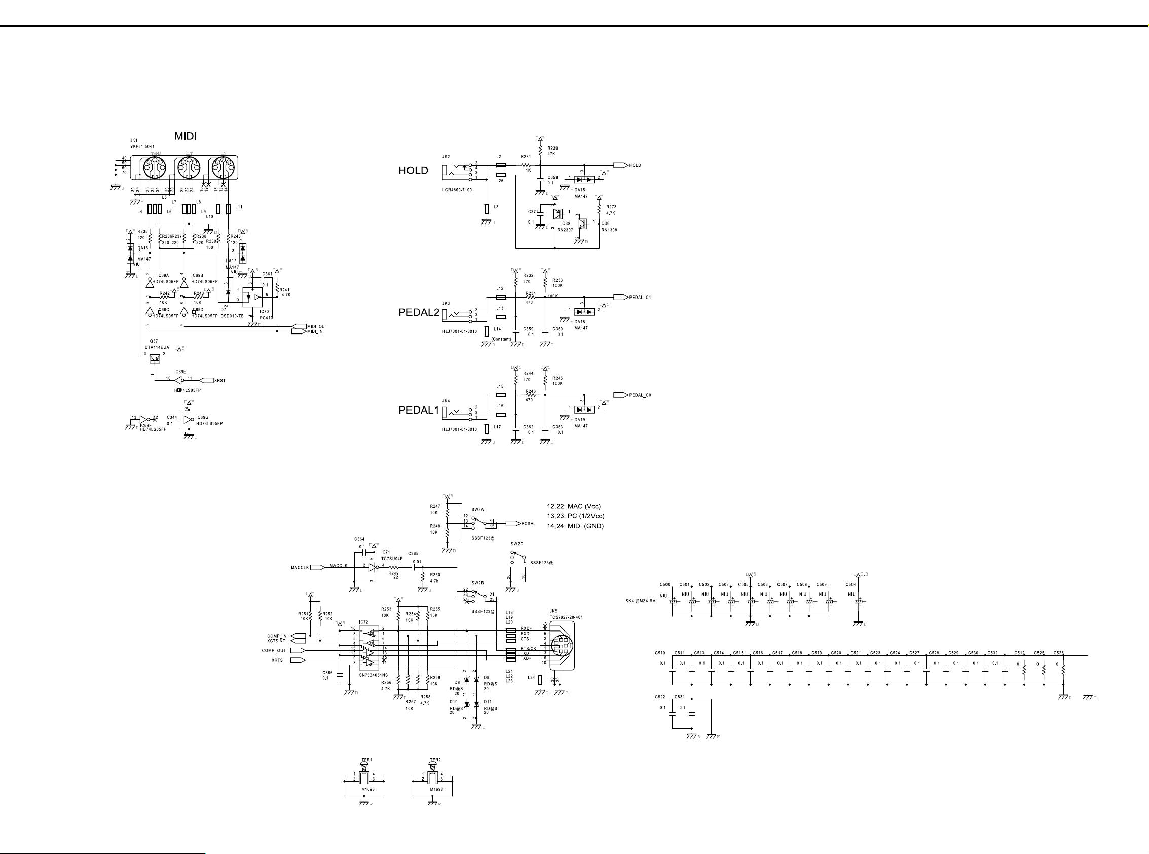
MAR, 2000 XV-88
12345678910111213141516171819202122232425262728
A
B
C
D
E
F
G
H
I
J
MAIN BOARD
K
L
M
N
O
P
Q
R
S
T
U
29
Page 30

XV-88 MAR, 2000
12345678910111213141516171819202122232425262728
A
B
C
D
E
F
G
H
I
J
PANEL BOARD
K
L
M
N
O
P
Q
R
S
30
T
U
Page 31

MAR, 2000 XV-88
12345678910111213141516171819202122232425262728
A
B
C
D
E
F
G
H
I
J
PANEL BOARD
K
L
M
N
O
P
Q
R
S
T
U
31
Page 32

XV-88 MAR, 2000
12345678910111213141516171819202122232425262728
A
B
C
D
E
F
G
H
I
J
EXP BOARD
K
L
M
N
O
P
Q
R
S
32
T
U
Page 33

MAR, 2000 XV-88
12345678910111213141516171819202122232425262728
A
B
C
D
E
F
G
H
I
J
EXP BOARD
K
L
M
N
O
P
Q
R
S
T
U
33
Page 34

XV-88 MAR, 2000
12345678910111213141516171819202122232425262728
A
B
C
D
E
F
G
H
I
J
ANALOG BOARD
K
L
M
N
O
P
Q
R
S
34
T
U
Page 35

MAR, 2000 XV-88
ERROR MESSAGES
Battery Low
Situation: The internal backup battery that is preserving the contents of
Action: Consult your dealer or a nearby Roland service station to have
File Format Error
Situation: The XV-88 cannot handle this file.
File I/O Error
Situation: It was not possible to save/load a file.
Action: Try the operation once again. If the same message appears,
File Name Duplicate
Situation: A file of the same name exists on the memory card.
Action: Use a different file name.
File Name Format Error
Situation: A file name has not been assigned.
Action: Assign a file name.
user memory has run down.
the battery replaced.
that file has been damaged. Delete the damaged file.
エラー・メッセージ
エラー・メッセージ
エラー・メッセージエラー・メッセージ
操作に誤りがあったり、操作どおりに正しく処理できなかったりしたとき
は、ディスプレイにエラー・メッセージが表示されます。
表示されたエラー・メッセージの指示にしたがって、対処してください。
エラー・メッセージはアルファベット順に並べています。
Battery Low
原因: 本体内のバックアップ・バッテリー(ユーザー・メモリーの
データを保持するための電池)の寿命です。
対応: お買い上げ店または最寄りのローランド・サービスに電池の交
換を依頼してください。
File Format Error
原因: XV-88 では扱えないファイルです。
File I/O Error
原因: ファイルのセーブ/ロードができません。
対応: もう一度操作を繰り返してください。同じメッセージが表示され
る場合、そのファイルは壊れているので削除してください。
File Name Duplicate
原因: メモリー・カードに同じ名前のファイルがあります。
対応: ファイル・ネームを変更してください。
File Name Format Error
原因: ファイル・ネームが付いていません。
対応: ファイル・ネームを付けてください。
MIDI Communication Error
Situation: A problem has occurred with the MIDI cable connections.
Action: Check that MIDI cables are not broken or pulled out.
Receive Data Error
Situation: A MIDI message was received incorrectly.
Action: If the same error message is displayed repeatedly, there is a
problem with the MIDI messages that are being transmitted
to the XV-88.
Unformatted Memory Card
Situation: This memory card cannot be used by the XV-88.
Action: Format the memory card on the XV-88.
User Memory Damaged
Situation: The data in user memory has been lost.
Action: Use the Factor Reset function (UTILITY/UTIL 2/FACTORY
RESET) to initialize the memory to the factory settings.
User Memory Write Protected
Situation 1: The Internal parameter (UTILITY/UTIL 1/PROTECT/
Action 1: Turn the Internal parameter OFF.
Situation 2: The Exclusive parameter (UTILITY/UTIL 1/PROTECT/
Action 2: Turn the Exclusive parameter OFF.
WRITE PROTECT) is turned ON.
WRITE PROTECT) is turned ON, and Exclusive messages
cannot be received.
MIDI Communication Error
原因: MIDI ケーブルの接続に問題があります。
対応: MIDI ケーブルの抜けや断線がないことを確認してください。
Receive Data Error
原因: MIDI メッセージが正しく受信できませんでした。
対応: 何度も同じメッセージが表示されるときは、MIDI メッセージ
の内容に問題があります。
Unformatted Memory Card
原因: XV-88 では扱えないメモリー・カードです。
対応: XV-88 でメモリー・カードをフォーマットしてください。
User Memory Damaged
原因: ユーザー・メモリーのデータが壊れています。
対応: FACTORY RESET 機能(UTILITY/UTIL 2/FACTORY RESET)の操作
で、お買い上げ時の設定に戻してください。
User Memory Write Protected
原因 1: Internal パラメーター(UTILITY/UTIL 1/PROTECT/WRITE
PROTECT)がオンに設定されています。
対応 1: Internal パラメーターをオフにしてください。
原因 2: Exclusive パラメーター(UTILITY/UTIL 1/PROTECT/WRITE
PROTECT)がオンに設定されているため、エクスクルーシ
ブ・メッセージを受信できません。
対応 2: Exclusive パラメーターをオフにしてください。
File not Found
Situation: The specified file was not found.
Action: Insert the memory card that contains the specified file, and try
the operation once again.
Memory Card Full
Situation: There is insufficient space available on the memory card to
Action: Either insert a different memory card, or delete unnecessary
save the data.
data and try the operation once again.
Memory Card I/O Error
Situation: It is possible that the memory card has been scratched or oth-
Action: If the memory card has been damaged, do not use that mem-
erwise damaged.
ory card. If the same error message appears repeatedly, consult your dealer or a nearby Roland service station.
Memory Card not Ready
Situation: A memory card is not inserted in the MEMORY CARD slot.
Action: Turn off the power, and insert a memory card.
Memory Card Write Protected
Situation: Since a write protect sticker is affixed to the memory card, data
Action: Remove the write protect sticker from the memory card.
cannot be saved to the card bank.
MIDI Buffer Full
Situation: Due to an inordinate volume of MIDI messages received, the
Action: Reduce the amount of MIDI messages to be transmitted.
XV-88 has failed to process them properly.
File not Found
原因: 指定のファイルが見つかりません。
対応: 指定のファイルが入っているメモリー・カードに入れ替えて操
作し直してください。
Memory Card Full
原因: メモリー・カードの空き容量が不足しているため、データを保
存できません。
対応: 他のメモリー・カードに入れ替えるか、不要なデータを削除し
てから操作し直してください。
Memory Card I/O Error
原因: メモリー・カードに傷が付いている可能性があります。
対応: メモリー・カードに傷が付いているときは、そのメモリー・
カードを使わないようにしてください。同じメッセージが何度
も表示されるときは、お買い上げ店または最寄りのローランド・
サービスに修理を依頼してください。
Memory Card not Ready
原因: MEMORY CARD スロットにメモリー・カードが入っていません。
対応: いったん電源を切って、メモリー・カードを入れてください。
Memory Card Write Protected
原因: メモリー・カードにライト・プロテクト・シールが貼られてい
るため、カード・バンクへ保存できません。
対応: メモリー・カードのライト・プロテクト・シールを剥がしてか
ら操作し直してください。
MIDI Buffer Full
原因: 受信した MIDI メッセージの量が多いため、正しく処理できませ
んでした。
対応: 送信する MIDI メッセージの量を減らしてください。
35
Page 36

 Loading...