

Page 1
XV-5080 JUN. 2000
TABLE OF CONTENTS 目次
SPECIFICATIONS . . . . . . . . . . . . . . . . . . .
LOCATION OF CONTROLS . . . . . . . . . . .
LOCATION OF CONTROLS PARTS LIST
EXPLODED VIEW . . . . . . . . . . . . . . . . . . .
EXPLODED VIEW PARTS LIST . . . . . . . .
PARTS LIST . . . . . . . . . . . . . . . . . . . . . . . .
IDENTIFYING THE VERSION NUMBER
USER DATA SAVE AND LOAD . . . . . . . . .
FACTORY PRESET . . . . . . . . . . . . . . . . . .
HOW TO VERSION UP THE FLASH ROM
TEST MODE. . . . . . . . . . . . . . . . . . . . . . . .
BLOCK DIAGRAM . . . . . . . . . . . . . . . . . . .
CIRCUIT BOARD . . . . . . . . . . . . . . . . . . . .
CIRCUIT DIAGRAM . . . . . . . . . . . . . . . . . .
ERROR MESSAGES . . . . . . . . . . . . . . . . .
目次 Page
目次目次
スペック/主な仕様
パネル配置図
. . .
パネル配置図パーツリスト
分解図
分解図パーツリスト
パーツリスト
. . .
バージョンナンバーの確認方法
データのセーブとロード
ファクトリーリセットの方法
. . .
フラッシュ ROM バージョンアップの方法
テストモード
ブロック図・配線図
基板図
回路図
エラー・メッセージ
. . . . . . . . . . . . . . . . . . . . . . 1
. . . . . . . . . . . . . . . . . . . . . . . . . . . . 2
. . . . . . . . . . . . . . . . . 2
. . . . . . . . . . . . . . . . . . . . . . . . . . . . . . . . . 3
. . . . . . . . . . . . . . . . . . . . . . 3
. . . . . . . . . . . . . . . . . . . . . . . . . . 4-7
. . . . . . . . . . . . . 8
. . . . . . . . . . . . . . . . . . . 8
. . . . . . . . . . . . . . . 9
. . . 9-10
. . . . . . . . . . . . . . . . . . . . . . . . 10-14
. . . . . . . . . . . . . . . . . . . . . 15
. . . . . . . . . . . . . . . . . . . . . . . . . . . . . 16-21
. . . . . . . . . . . . . . . . . . . . . . . . . . . . . 22-37
. . . . . . . . . . . . . . . . . . 38-39
SPECIFICATIONS
XV-5080 128 voice sound module
GM Level 2 system Compatible
Parts
32
Maximum Polyphony
128 voices
Wave memory
64MB (16-bit linear format)
Expansion slots
Wave Expansion Board
SR-JV80 Series: 4slots
New Wave Expansion Board
SRX Series: 4slots
Two SIMM Slots (Compatible
with 72-pin FP/EDO 16/32/64
MB SIMMs for a maximum
expansion of 128 MB)
Preset memory
Patch: 896 (128 x 7 banks) +
GM Level 2 Patch: 256
Performance: 64 (32 x 2 banks)
Rhythm Sets: 14 (2 x 7 banks)
+ GMLevel 2 Rhythm Set: 9
User memory
Patch: 128
Performance: 64
Rhythm Set: 4
External memory
SmartMedia card 1slot
( 2 - 128 MB, 5 or 3.3 V)
Effects
Multi Effects (MFX): 90 type
(Three different multi-effects
can be used simultaneously in
Performance mode)
Reverb: 4 type
Chorus: 2 type
2 Band EQ
(can be sent to eight separate outputs when used as system EQ)
Display
320 x 80 dot Graphic LCD
(with Backlit )
Connectors
A (MIX) Output (L(MONO), R)
B Output (L, R)
C Output (L, R)
D Output (L, R)
(or Individual 1 - 8)
Digital Audio Out S/P DIF 44.1/
48kHz (COAXIAL 1, OPTICAL 1)
Word Clock In (BNC)
SCSI Connector (D-SUB 25pin)
R-BUS Connector (Output Only)
MIDI connector (IN, OUT, THRU)
Phones Jack (Stereo)
Power supply
AC117, 230, 240 V
Power Consumption
25 W
Dimensions
482 (W) x 281 (D) x 88 (H) mm
19 (W) x 11-1/16 (D) x 3-1/2 (H)
inches
(EIA-2U rack mount type)
Weight
4.9 kg / 10lbs 13oz
Accessories
Owner's manual
English:(71566556)
Japanese:(71563812)
Power cord
100V:(00894367)
120V:(00894378)
230V:(00894389)
240VE:(00907001)
240VA:(23495124)
Options
Wave Expansion Board
(SRX series, SR-JV80 series)
* In the interest of product
improvement, the specifications
and/or appearance of this unit
are subject to change without
prior notice.
Owner's manual includes
the following parts.
Quickstart manual
Q&A, Sound List
スペック・主な仕様
スペック・主な仕様
スペック・主な仕様スペック・主な仕様
XV-5080:128 ボイス・サウンド・モジュール
XV-5080:128 ボイス・サウンド・モジュール
XV-5080:128 ボイス・サウンド・モジュールXV-5080:128 ボイス・サウンド・モジュール
●
パート
パート
パートパート
32
●
最大同時発音数
最大同時発音数
最大同時発音数最大同時発音数
128 音
●
波形メモリ
波形メモリ
波形メモリ波形メモリ
64MB (16 ビットリニア換算 )
●
拡張スロット
拡張スロット
拡張スロット拡張スロット
ウェーブ・エクスパンション・ボード
SR-JV80 シリーズ 最大 4 枚
新ウェーブ・エクスパンション・
ボード SRX シリーズ 最大 4 枚
SIMM スロット 2 (72pin FP/
EDO 16/32/64MB SIMM に対応、
最大 128MB まで拡張可能 )
●
プリセット・メモリー
プリセット・メモリー
プリセット・メモリー プリセット・メモリー
パッチ 896 (128 × 7 バンク)
+ GM レベル 2 パッチ 256
パフォーマンス 64
(32 × 2 バンク )
リズムセット 14 (2 × 7 バンク)
+ GM レベル 2 リズムセット 9
●
ユーザー・メモリー
ユーザー・メモリー
ユーザー・メモリーユーザー・メモリー
パッチ 128
パフォーマンス 64
リズムセット 4
●
外部メモリー
外部メモリー
外部メモリー外部メモリー
スマート・メディア・カード 1
スロット ( 2 - 128MB、5/3.3
V 両対応 )
●
エフェクト
エフェクト
エフェクトエフェクト
マルチ・エフェクト 90 種類
( パフォーマンス・モードでは 3 種
類の異なる EFX を同時に使用可 )
リバーブ 4 種類
コーラス 2 種類
2 バンド EQ 1
(システム EQ として8個の各
アウトプットに機能)
●
ディスプレイ
ディスプレイ
ディスプレイディスプレイ
320 × 80 ドットグラフィック
LCD ( バックライト付き )
●
接続端子
接続端子
接続端子接続端子
A(MIX) アウトプット
(L(MONO), R)
B アウトプット (L, R)
C アウトプット (L, R)
D アウトプット (L, R) もしく
はインディビデュアル 1 - 8
デジタル・オーディオ・アウ
ト S/P DIF 44.1/48kHz
(COAXIAL 1, OPTICAL 1)
ワードクロック・イン 1 (BNC)
SCSI 端子 1 (D-SUB 25 ピン )
R-BUS 1 (アウトプットのみ)
MIDI コネクター
(IN 1/2, OUT, THRU (IN1))
ヘッドホン・ジャック
AC イン
●
電源
電源
電源電源
AC100/117/230/240V, 50/60Hz
●
消費電力
消費電力
消費電力消費電力
25W
●
外形寸法
外形寸法
外形寸法外形寸法
482 ( 幅 ) x 281 ( 奥行 ) x 88
( 高さ ) mm (EIA-2U ラック・
マウント・タイプ )
●
重量
重量
重量重量
4.9 kg
●
付属品
付属品
付属品付属品
取扱説明書
和文:(71563812)
英文:(71566556)
以下冊子を含みます
クイック・スタート
Q&A
電源コード:(00894367)
●
別売品
別売品
別売品別売品
ウェーブ・エクスパンション・ボード
(SRX シリーズ、SR-JV80 シリーズ )
MIDI/SYNC ケーブル
(MSC-15/25/50)
17059030 Printed in Japan AA00 (NB)
Page 2
XV-5080 JUN. 2000
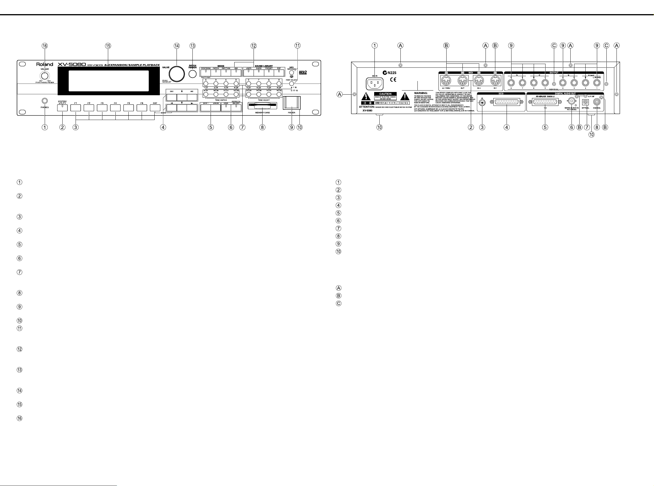
LOCATION OF CONTROLS / パネル配置図
LOCATION OF CONTROLS PARTS LIST / パネル配置図パーツリスト
Front panel parts list /
NO. PART CODE PART NAME DESCRIPTION Q'TY
01129145 6.5MM JACK STEREO YKB21-5268(=YKB21-5255) 1
12199556 JACK SNAP MET41-0105 1
02011412 Y S-KEYTOP SD1H BLK 1
00348490 LED (RED) SLR-325VCT31 1
02125945 TACT SWITCH EVQ 11G 05R 1
02011456 Y S-KEYTOP SX1H BLK 7
02125945 TACT SWITCH EVQ 11G 05R 7
02011478 Y S-KEYTOP SX3H BLK 2
02125945 TACT SWITCH EVQ 11G 05R 6
02011467 Y S-KEYTOP SX2H BLK 1
02125945 TACT SWITCH EVQ 11G 05R 2
02011423 Y S-KEYTOP SD2H BLK 1
02125945 TACT SWITCH EVQ 11G 05R 2
01780834 F C-KEYTOP SX4H CLR 4
02125945 TACT SWITCH EVQ 11G 05R 1
00560745 LED (GREEN) SLR-325MCT31 16
01786712 ESCUTCHEON 1
01780712 CARD CONECTR CN015P-3013-0 1
22495565 F S-BUTTON MX BLK 1
02013567 PUSH SWITCH ESB92S21B TV-5 5A/250V 1
01459789 BUTTON ESCUTCHEON F B-ESCT MX1H-A BLK 1
01670490 F C-KEYTOP SX1H CLR 2
02125945 TACT SWITCH EVQ 11G 05R 1
00560745 LED (GREEN) SLR-325MCT31 2
02011445 Y S-KEYTOP SD4H BLK 4
02125945 TACT SWITCH EVQ 11G 05R 1
00348490 LED (RED) SLR-325VCT31 16
02013090 F C-KEYTOP MX1H CLR 1
02125945 TACT SWITCH EVQ 11G 05R 1
02011856 LED (ORG) SLR-56DCT32 1
22480321 S R-KNOB L BLK 248-321 1
02014145 ROTARY ENCODER EC16B36244 (L=20.DCUT=7) 1
02128689 LCD RCM6048T-A 1
22065240 DISPLAY COVER 206-240 1
01899212 P R-KNOB MF-A BLK/LCG 1
02013656 9M/M ROTARY POTENTIOMETER RK0971224 10KBX2 W/SW 1
フロントパネルパーツリスト
フロントパネルパーツリスト
フロントパネルパーツリストフロントパネルパーツリスト
パネル配置図
パネル配置図パネル配置図
パネル配置図パーツリスト
パネル配置図パーツリストパネル配置図パーツリスト
Rear panel parts list /
No. PART CODE PART NAME DESCRIPTION Q'TY
01901801 WIRING W7 1
13429676 MIDI CONNECTOR YKF51-5048 (TWIN) 2
02128367 ROTARY DIGITAL SWITCH KWC10H 1
02019667 D-SUB CONNECTOR YKF42-8035 1
01898389 D-SUB CONNECTOR YKF42-8034 1
02120734 BNC CONNECTOR COH2201-A 1
01239078 IC (OPTICAL DIGITAL OUT) TOTX178A 1
01343723 RCA(PIN) JACK YKC21-3117(ORANGE) 1
13449283 6.5MM JACK HLJ7101-01-3010 8
12359137 RUBBER FOOT SJ-5012 BLK 4
リアーパネルパーツリスト
リアーパネルパーツリスト
リアーパネルパーツリストリアーパネルパーツリスト
[SCREW]
No. PART CODE PART NAME DESCRIPTION Q'TY
40011090 SCREW 3X6 BINDING TAPTITE B BZC 5
40011312 SCREW 3X8 BINDING TAPTITE P BZC 7
40011501 SCREW M3X8 PAN MACHINE W/SW+PW BZC 2
2
Page 3
JUN. 2000 XV-5080
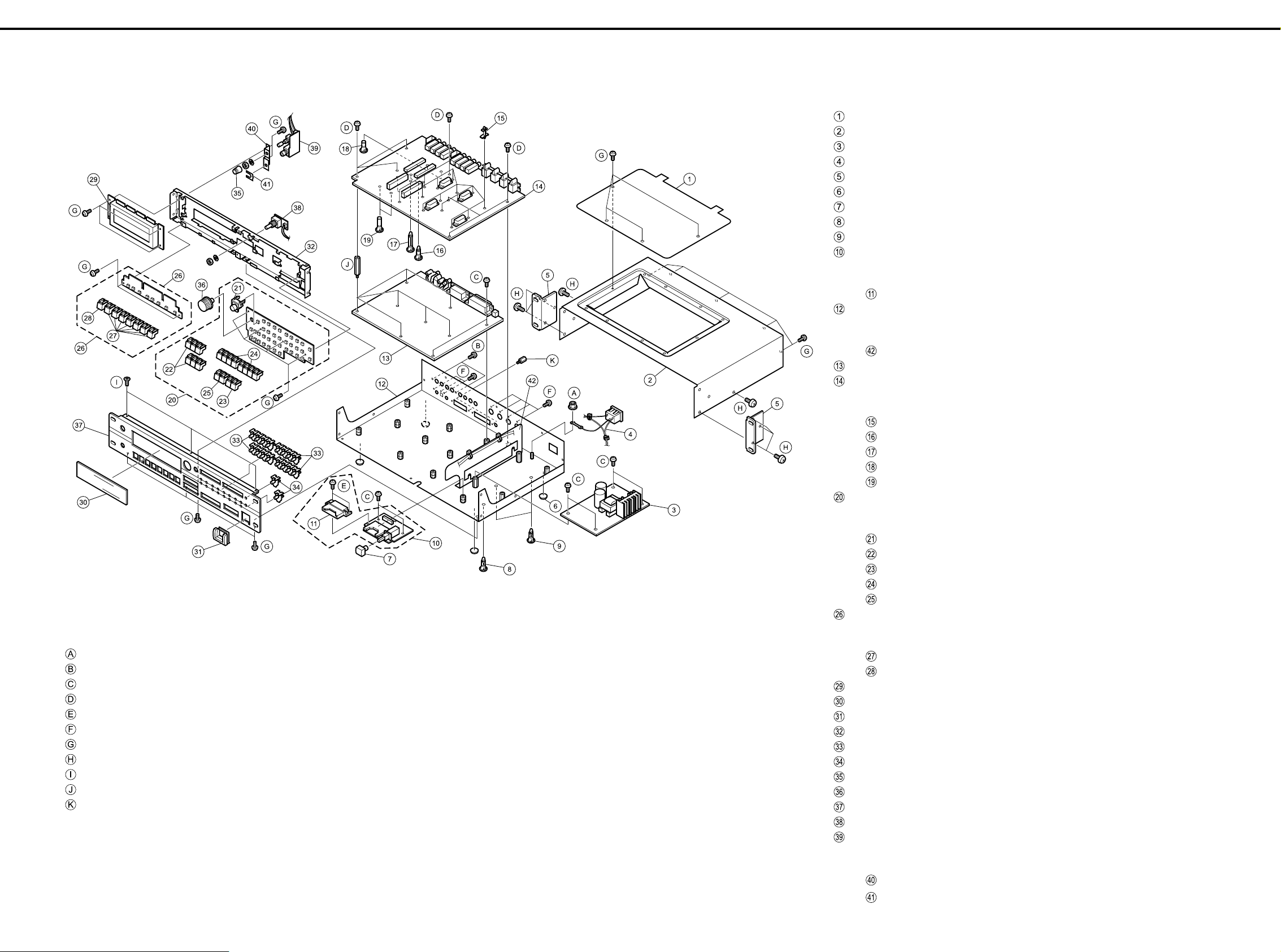
EXPLODED VIEW / 分解図
分解図
分解図分解図
[SCREW]
NO. PART CODE PART NAME DESCRIPTION Q'TY
40011745 HEX NUT M4 SPRING NUT ZC 1
40011501 SCREW M3X8 PAN MACHINE W/SW+PW BZC 2
40013067 SCREW M3X8 PAN MACHINE W/SW+SMALL PW ZC 8
40015945 SCREW 3X8 BINDING TAPTITE S ZC 9
40011278 SCREW 3X8 BINDING TAPTITE P ZC 2
40011312 SCREW 3X8 BINDING TAPTITE P BZC 7
40011090 SCREW 3X6 BINDING TAPTITE B BZC 25
40012345 SCREW 4X10 BINDING TAPTITE B BZC 8
40011156 SCREW 3X8 FLAT TAPTITE B BZC 3
02126734 BOSS NUT M3/M3 L28.6 7
This part is included the following part.
このパーツは、以下の部品に含まれます。
02019667 YKF12-8035 D-SUB CONNECTOR
01898389 YKF42-8034 D-SUB CONNECTOR
EXPLODED VIEW PARTS LIST / 分解図パーツリスト
分解図パーツリスト
分解図パーツリスト分解図パーツリスト
[PART]
NO. PART CODE PART NAME DESCRIPTION Q'TY
02013212 EXP COVER 1
02013201 TOP COVER 1
01121234 SWITCHING REGULATOR RH2 1
01901801 WIRING W7 1
22125586 RACK ANGLE 2U 2
12359137 RUBBER FOOT SJ-5012 BLK 4
22495565 F S-BUTTON MX BLK 1
12199562 PCB SPACER KGLS-10R (BLACK) 1
02236456 PCB SPACER KGLS-14RT 2
71563878 MEDIA ASSY 1
MEDIA ASSY inculde the following parts
MEDIA ASSY
01786712
71672990 BOTTOM CHASSIS ASSY 1
BOTTOM CHASSIS ASSY inculde the following parts
BOTTOM CHASSIS ASSY
02013078
71563845 MAIN BOARD ASSY (EXG) 1
71563867 EXP BASE BOARD ASSY 1
EXP BASE BOARD ASSY includes the following parts.
EXP BASE BOARD ASSY 下記の部品を含みます。
12189810
02019034
02120434
01902756
02120445
71563901 PANEL-A KEYTOP ASSY 1
PANEL-A KEYTOP ASSY includes the following parts.
PANEL-A KEYTOP ASSY
02013090
02011478
02011423
02011445
02011467
71563923 PANEL-B KEYTOP ASSY 1
PANEL-B KEYTOP ASSY includes the following parts.
PANEL-B KEYTOP ASSY
02011456
02011412
02128689 LCD RCM6048T-A 1
22065240 DISPLAY COVER 206-240 1
01459789 BUTTON ESCUTCHEON F B-ESCT MX1H-A BLK 1
02019745 FRONT HOLDER 1
01780834 F C-KEYTOP SX4H CLR 4
01670490 F C-KEYTOP SX1H CLR 2
01899212 P R-KNOB MF-A BLK/LCG 1
22480321 S R-KNOB L BLK 248-321 1
02019734 FRONT PANEL 1
71563945 ENCODER BOARD ASSY 1
71563956 PHONES HOLDER ASSY 1
PHONES HOLDER ASSY includes the following parts.
PHONES HOLDER ASSY
02236567 PHONES HOLDER
12199556 JACK SNAP MET41-0105
は以下の部品を含みます。
ESCUTCHEON 1
は以下の部品を含みます。
PWR SPLY COVER 1
PCB SPACER WLS-14-094VO 12
PWB SPACER RSPLS-12L 2
PWB SPACER RSPLS-18L 2
PWB SPACER RSPS-12L 2
PWB SPACER RSPS-18L 2
は以下の部品を含みます。
F C-KEYTOP MX1H CLR 1
Y S-KEYTOP SX3H BLK 2
Y S-KEYTOP SD2H BLK 1
Y S-KEYTOP SD4H BLK 2
Y S-KEYTOP SX2H BLK 1
は以下の部品を含みます。
Y S-KEYTOP SX1H BLK 7
Y S-KEYTOP SD1H BLK 1
は以下の部品を含みます。
1
3
Page 4
XV-5080 JUN. 2000
PARTS LIST / パーツリスト
SAFETY PRECAUTION:*1
The parts marked have safety-related
characteristics. Use only listed parts for
replacement.
安全上の注意:*1
が付いている部品は、安全上特別な規
格でつくられたものです。
交換の際は、指定された部品番号以外の部
品は使わないようにして下さい。
NOTE: Consider about the natural environment carefully before through the old lithium battery away when you exchange to the new one.
注意: リチウム電池の交換時に、不要になったリチウム電池は、環境問題を十分考慮した上で処理して下さい。
*1 *2
CASING /
22125586 RACK ANGLE 2U 2
02013212 EXP COVER 1
02013201 TOP COVER 1
22065240 DISPLAY COVER 206-240 1
01459789 BUTTON ESCUTCHEON F B-ESCT MX1H-A BLK 1
# 02019734 FRONT PANEL 1
CHASSIS /
# 71672990 BOTTOM CHASSIS ASSY 1
NOTE: 'BOTTOM CHASSIS ASSY' includes the following parts.
注意 : 補修用 BOTTOM CHASSIS ASSY は、下記の部品を含みます。
# 02019756 BOTTOM CHASSIS 1
02013078 PWR SPLY COVER 1
40011090 SCREW 3X6 BINDING TAPTITE B FE BZC 2
# 02019745 FRONT HOLDER 1
パーツリスト
パーツリストパーツリスト
The parts marked # are
new (ini tial parts). *2
# の付いた部品は新規部
品です。*2
ケース
ケース
ケースケース
シャーシ
シャーシ
シャーシシャーシ
CONSIDERATIONS ON PARTS ORDERING
When ordering any parts listed in th e parts list. please specify the following items in the order sheet.
QTY PART NUMBER DESCRIPTION MODEL NUMBER
Ex 10 22575241 Sharp key C-20/50
15 2247017300 Knob (orange) DAC-15D
Failure to completely fill the above items with correct number and description will result in delayed or
even undelivered replacement.
パーツ発注に関するお願い
オーダーシートには、必ず下記の4項目は正確に記入して下さい。(例外は除く)
必要数 パーツナンバー 品名 使用機種
例) 10 22575241 Sharp key C-20/50
15 2247017300 Knob (orange) DAC-15D
もし記入洩れ、誤記等が有る場合、必要部品が発送できなかったり、大幅な遅れの 原因になります。
御協力をお願いします。
Q'ty
DISPLAY UNIT /
# 02128689 RCM6048T-A LCD 1
NOTE: Replacement RCM6048T-A should be made on a unit base.
注意 : RCM6048T-A の交換は、ユニット単位で行って下さい。補修品は、ユニット単位。
POWER SUPPLY UNIT /
01121234 RH2 SWITCHING REGULATOR 1
NOTE: Replacement RH2 should be made on a unit base.
注意 : RH2 の交換は、ユニット単位で行って下さい。補修品は、ユニット単位。
PCB ASSY /
# 71563845 MAIN BOARD ASSY (EXG) 1
NOTE: 'MAIN BOARD ASSY' includes the following parts.
注意 : 補修用 MAIN BOARD ASSY は、下記の部品を含みます。
# 02233178 RIBBON CABLE 6X120-P2.0 1
40342856 COATING CLIP CP-1S 1
# 71563867 EXP BASE BOARD ASSY 1
NOTE: 'EXP BASE BOARD ASSY' includes the following parts.
注意 : 補修用 EXP BASE BOARD ASSY は、下記の部品を含みます。
12189810 PCB SPACER WLS-14-094VO 12
02019034 PWB SPACER RSPLS-12L 2
# 02120434 PWB SPACER RSPLS-18L 2
# 02120445 PWB SPACER RSPS-18L 2
01902756 PWB SPACER RSPS-12L 2
12199584 GROUNDING TERMINAL M1698 TER2,TER1 on EXP Base Board 2
40342856 COATING CLIP CP-1S 1
# 71563878 MEDIA ASSY 1
NOTE: 'MEDIA ASSY' includes the following parts.
注意 : 補修用 MEDIA ASSY は、下記の部品を含みます。
01786712 ESCUTCHEON 1
40011278 SCREW 3X8 BINDING TAPTITE P FE ZC 2
表示ユニット
表示ユニット
表示ユニット表示ユニット
基板完成品
基板完成品
基板完成品基板完成品
電源ユニット
電源ユニット
電源ユニット電源ユニット
KNOB, BUTTON /
22495565 F S-BUTTON MX BLK 1
01670490 F C-KEYTOP SX1H CLR 2
01780834 F C-KEYTOP SX4H CLR 4
01899212 P R-KNOB MF-A BLK/LCG 1
22480321 S R-KNOB L BLK 248-321 1
SWITCH /
# 02128367 KWC10H ROTARY DIGITAL SWITCH SW2 on Main Board 1
02013567 ESB92S21B TV-5 5A/250V PUSH SWITCH SW46 on Media Board 1
# 02125945 EVQ 11G 05R TACT SWITCH on Panel A, on PanelB
スイッチ
スイッチ
スイッチスイッチ
JACK, EXP TERMINAL /
# 02120734 BNC CONNECTOR COH2201-A JK2 on Main Board 1
01343723 YKC21-3117(ORANGE) RCA(PIN) JACK JK1 on Main Board 1
# 02019667 YKF42-8035 D-SUB CONNECTOR CN9 on Main Board 1
01898389 YKF42-8034 D-SUB CONNECTOR CN8 on Main Board 1
13429676 YKF51-5048 (TWIN) MIDI CONNECTOR JK8,JK4 on EXP Base Board 2
13449283 HLJ7101-01-3010 6.5MM JACK JK1,JK10,JK9,JK7,JK6,JK5,JK2,
01780712 CN015P-3013-0 CARD CONECTR CN7 on Media Board 1
01129145 YKB21-5268(=YKB21-5255) 6.5MM JACK STEREO JK1 on Phones Board 1
つまみ、ボタン
つまみ、ボタン
つまみ、ボタンつまみ、ボタン
ジャック、外部接続端子
ジャック、外部接続端子
ジャック、外部接続端子ジャック、外部接続端子
37+8
JK3 on EXP Base Board
# 71563901 PANEL-A KEYTOP ASSY 1
NOTE: 'PANEL-A KEYTOP ASSY' includes the following parts.
注意 : 補修用 PANEL-A KEYTOP ASSY は、下記の部品を含みます。
# 02011423 Y S-KEYTOP SD2H BLK 1
02011445 Y S-KEYTOP SD4H BLK 2
# 02011467 Y S-KEYTOP SX2H BLK 1
02011478 Y S-KEYTOP SX3H BLK 2
02013090 F C-KEYTOP MX1H CLR 1
# 71563956 PHONES HOLDER ASSY 1
NOTE: 'PHONES HOLDER ASSY' includes the following parts.
注意 : 補修用 PHONES HOLDER ASSY は、下記の部品を含みます。
# 02236567 PHONES HOLDER 1
12199556 JACK SNAP MET41-0105 1
# 02019689 WIRING 11X125-P2.0-SB20-JB20-F CN5 on Phones Board 1
40342856 COATING CLIP CP-1S 1
# 71563923 PANEL-B KEYTOP ASSY 1
NOTE: 'PANEL-B KEYTOP ASSY' includes the following parts.
注意 : 補修用 PANEL-B KEYTOP ASSY は、下記の部品を含みます。
8
02011412 Y S-KEYTOP SD1H BLK 1
# 02011456 Y S-KEYTOP SX1H BLK 7
# 71563945 ENCODER BOARD ASSY 1
NOTE: 'ENCODER BOARD ASSY' includes the following parts.
注意 : 補修用 ENCODER BOARD ASSY は、下記の部品を含みます。
# 02019678 WIRING 4X125-P2.0-SB20-JB20-F CN2 on Encoder Board 1
4
Page 5

JUN. 2000 XV-5080
IC
01672867 M38881M2-069FP IC CPU IC107 on Main Board 1
# 02015556 HD6437042AA13F VER1.00 IC (32BIT CPU) IC3 on Main Board 1
00893356 SYM53CF92 IC (SIO) IC53 on Main Board 1
# 01455956 TC223C660CF-503 IC (RA08-503) IC12,IC13 on Main Board 2
01342978 TC160G22AF-1253 IC (CUSTOM) IC4 on Main Board 1
01902212 UPD431000AGW-70LL-E2 IC (SRAM) IC6,IC84 on Main Board 2
01125112 TC55257DFL-70L(EL) IC (SRAM) IC52 on Main Board 1
02010290 VG2618165CJ-6-EL-10 IC (DRAM) IC19,IC18 on Main Board 2
# 01784023 MSM5117805D-60JSR1 IC (DRAM) IC118,IC117 on Main Board 2
02010056 UPD23C128040LGY-850-MJH IC (MASK ROM) IC29 on Main Board 1
02010023 UPD23C128040LGY-849-MJH IC (MASK ROM) IC26 on Main Board 1
01561945 LH28F160S5T-L70 IC (FLASH MEMORY) IC1 on Main Board 1
01451578 AK4324-VF-E2 IC (DAC) IC71,IC74,IC79,IC82 on Main Board 4
01901989 TC7SET04F(TE85L) IC (CMOS) IC112,IC113 on Main Board 2
15259884 TC7S08F(TE85L) IC (CMOS) IC50,IC76 on Main Board 2
15259823T0 TC74HC574AF(EL) IC (CMOS) IC58 on Main Board 1
15259809T0 TC74HC393AF(EL) IC (CMOS) IC86 on Main Board 1
# 02017034 TC7W53FU(TE12L) IC (COMS)
15249111 TC7WU04F(TE12L) IC (CMOS) IC17,IC15,IC7,IC55 on Main Board 4
15249104 TC7S04F(TE85L) IC (CMOS) IC54,IC111 on Main Board 2
15249112 TC7W32F(TE12L) IC (CMOS) IC85,IC110 on Main Board 2
15259708T0 TC74HC08AF(TP2) IC IC116 on Main Board 1
15259720T0 TC74HC74AF(TP2) IC (HS-CMOS) IC115 on Main Board 1
15259726T0 TC74HC107AF IC IC23 on Main Board 1
15259769T0 TC74HC238AF(EL) IC (CMOS) IC57 on Main Board 1
00232645 TC7W14F(TE12L) IC (CMOS) IC114 on Main Board 1
15259706T0 TC74HCU04AF(EL) IC (HS-CMOS) IC41 on Main Board 1
15259716T0 TC74HC32AF(TP2) IC (HS-CMOS) IC63 on Main Board 1
# 15259752T0 TC74HC163AF(EL) IC (COMS) IC40,IC39 on Main Board 2
00346490 TC3W01F(TE12L) IC (CMOS) IC25 on Main Board 1
00893967 TC74VHC153F(EL) IC (CMOS) IC16 on Main Board 1
01121845 TC7W04FU TE12L IC (CMOS) IC101 on Main Board 1
01341578 TC74VHC14F(EL) IC (TTL SCHMITT TRIGGER INV.) IC48 on Main Board 1
00127490 TC7W08F(TE12L) IC (CMOS) IC105,IC8 on Main Board 2
# 02017056 TC74VHC126F(EL) IC (COMS) IC43 on Main Board 1
00564545 TC74VHC04F(EL) IC (CMOS)
# 02017045 TC74VHCT541AFT(EL) IC (COMS) IC28,IC27 on Main Board 2
01670789 TC74VHCT08AF IC (CMOS) IC60 on Main Board 1
00893978 TC74VHC393F(EL) IC (CMOS) IC20 on Main Board 1
01348956 TC7SH00FU(TE85L) IC (CMOS) IC109 on Main Board 1
01455312 TC7WH74FU IC (CMOS) IC37 on Main Board 1
00236878 TC74VHC74F-EL IC (CMOS) IC21,IC49,IC108 on Main Board 3
01783523 TC74VHCT245AFT(EL) IC (CMOS)
02124934 TC74VHC541FTEL IC (CMOS) IC103,IC62 on Main Board 2
15289106 M5238AFP-600C IC (JFET OP AMP) IC9 on Main Board 1
15289117 NJM5532MD-TE1 IC (OP AMP)
15189261 M5218AFP-600E IC (BIPOLAR OP AMP) IC69,IC11 on Main Board 2
15199137 AN7805F IC (V.RGL) IC77,IC68 on Main Board 2
15199286 AN78L05M-(E1) IC (REGULATOR) IC36,IC22 on Main Board 2
01899790 UPC29L33T-E2 IC (REGULATOR) IC66 on Main Board 1
01678512 UPC2933T-T2 IC REGULATOR IC14 on Main Board 1
15199284 PQ30RV1 IC (V.RGL) IC56 on Main Board 1
15199944 SED1335F0B IC (DRIVER) IC51 on Main Board 1
00892512 TLC2932IPW IC (PLL) IC24,IC42 on Main Board 2
01785178 TC9271FS IC IC38 on Main Board 1
15289123 M51953AFP-600C IC (RESET) IC10 on Main Board 1
01239078 TOTX178A IC (OPTICAL DIGITAL OUT) CN7 on Main Board 1
15269219H0 HD74LS05FPEL IC (TTL) IC37 on EXP Base Board 1
15259864T0 TC74HC4052AF(EL) IC (CMOS) IC15 on EXP Base Board 1
15249121 TC7W04F(TE12L) IC (CMOS) IC18 on EXP Base Board 1
IC30,IC32 on EXP Base Board ,IC45 on Main Board
IC16,IC38 on EXP Base Board ,IC46 on Main Board
IC9,IC11 on EXP Base Board ,IC104 on Main Board
IC73,IC70,IC83,IC81,IC80,IC78,IC75,IC72
on Main Board ,IC1 on Phones Board
1+2
1+2
1+2
8+1
01670734 TC74VHC541F IC (CMOS) IC26,IC24 on EXP Base Board 2
01906534 TC74VHCT32AF(EL) IC (CMOS) IC3,IC39 on EXP Base Board 2
01122267 TC74VHCT245F(EL) IC IC25,IC2,IC27 on EXP Base Board 3
# 02120367 TC74VHC11F(EL) IC (COMS) IC28,IC34 on EXP Base Board 2
00231889 TC74VHC32F(EL) IC (CMOS)
00236834 TC74VHC21F(EL) IC IC14 on EXP Base Board 1
00567534 TC74VHC138F(EL) IC (CMOS) IC4,IC1 on EXP Base Board 2
00670290 TC74VHC139F(EL) IC (CMOS)
00236845 TC74VHC245F(EL) IC (CMOS)
# 02016745 BA033FP-E2 IC (REGULATOR) IC23 on EXP Base Board 1
15289125 PC-410KT 178FAY IC (PHOTO COUPLER) IC36,IC35 on EXP Base Board 2
TRANSISTOR / トランジスター
15309113 2SA1213-O(TE12R.C) TRANSISTOR Q32 on Main Board 1
01121278 2SA1576A T106 QRS TRANSISTOR Q1 on Main Board 1
00901523 2SA1681 (SC-62)(POW SW) TRANSISTOR Q23 on Main Board 1
15319101 2SC2412KR T146 TRANSISTOR Q24,Q25 on Main Board 2
15319105 2SC3326-A TRANSISTOR Q17,Q20,Q19,Q30,Q18,Q29,Q21,
15319114 2SC2873-Y(TE12R.C) TRANSISTOR Q31 on Main Board 1
01783612 RN2426(TE85L) TRANSISTOR Q3,Q4,Q5,Q6,Q16 on Main Board 5
15329521 RN1307(TE85R) TRANSISTOR Q2,Q26 on Main Board 2
01451245 RN1414(TE85L) TRANSISTOR
15329503 DTA124EK T146 DIGITAL TRANSISTOR Q1 on EXP Base Board 1
DIODE / ダイオード
01780045 RB051L-40 SCHOTTKY DIODE D4,D3 on Main Board 2
01017512 RB411D T146 SCHOTTKY DIODE D8 on Main Board 1
02233890 DCB010-TB ARRAY DIODE D1 on Main Board 1
15339130 MA142WK-(TX) ARRAY DIODE DA4,DA15 on Main Board 2
01897189 MA147-(TX) ARRAY DIODE DA18,DA17,DA16,DA14,DA13,DA12,
01456456 UDZ TE-17 13B ZENER DIODE D5 on Main Board 1
15339119T0 1SS352(TPH3) SWITCHING DIODE D1,D2 on EXP Base Board 2
15339109 DAP202K T146 (CHIP) ARRAY DIODE DA4,DA1,DA2,DA3,DA5,DA6,DA7,
00348490 SLR-325VCT31 LED (RED)
00560745 SLR-325MCT31 LED (GREEN)
02011856 SLR-56DCT32 LED (ORG) LED25 on Panel-A Board 1
ダイオード
ダイオードダイオード
RESISTOR / 抵抗
00566867 RPC05T 100 J MTL.FILM RESISTOR R374,R402,R42,R41,R39,R24,R11,
15399713 MCR25 JZH J 101 MTL.FILM RESISTOR R141,R147,R140,R142,R143,R144,
01011856 RPC05T 0R0 J MTL.FILM RESIST0R
00566934 RPC05T 330 J MTL.FILM RESISTOR R22,R59 on Main Board 2
00567023 RPC05T 101 J MTL.FILM RESISTOR
00567289 RPC05T 103 J MTL.FILM RESISTOR
15399301 RPC10T 0R0 J MTL.FILM RESISTOR
トランジスター
トランジスタートランジスター
抵抗
抵抗抵抗
IC22,IC19,IC33,IC12 on EXP Base Board
IC20,IC21,IC29,IC17 on EXP Base Board
IC10,IC13,IC8,IC7,IC6,IC5 on EXP Base Board
Q22,Q27,Q28 on Main Board
Q8,Q11,Q9,Q13,Q12,Q14,Q7,Q10 on Main Board
DA3,DA2,DA11,DA1,DA6,DA7,DA8,
DA9,DA10 on Main Board
DA8,DA9,DA10,DA11,DA12,DA13,
DA14,DA15,DA16,DA17,DA19,DA18
on Panel-A Board,DA21,DA22,DA23,
DA20 on Panel-B Board
LED5,LED26,LED8,LED6,LED27,LED4,
LED3,LED2,LED1,LED7 on Panel-A
Board,LED30 on Panel-B Board
LED18,LED28,LED24,LED23,LED22,
LED21,LED20,LED19,LED16,LED14,
LED13,LED12,LED11,LED29,LED9,L
ED17,LED10,LED15 on Panel-A Board
R10,R40,R403 on Main Board
R145,R146 on Main Board
R56,R21,R20,R16,R9,R57,R112,R118,
R383,R360,R270,R224 on Main Board
R151,R338,R339,R385 on Main Board
R149,R36,R155,R160,R154,R150,R158,
R148,R114,R106,R54,R288,R382,R55,
R30,R405,R404,R401,R387,R379,R381,
R290,R378,R375,R373,R372,R371,R294,
R292,R159,R25,R23,R19,R7,R6,R5,R1,
R29,R284 on Main Board
C89,C101,R29,C121,C120,C119,C118,R2,
C104,C99,C96,C94,C87,R28,R5,R4,R3,C106
on EXP Base Board ,R179 on Main Board
10
15
19+4
10+1
18
10
12
39
1+18
4
4
6
8
8
4
5
Page 6

XV-5080 JUN. 2000
00566912 RPC05T 220 J MTL.FILM RESISTOR R116 on Main Board 1
15399349 RPC10T 100 J 1/10W MTL.FILM RESISTOR
15399469 RPC10T 105 J 1/10W MTL.FILM RESISTOR R393,R394 on Main Board 2
00566967 RPC05T 470 J MTL.FILM RESISTOR R103,R287,R286,R285,R283,R282,
00567001 RPC05T 750 J MTL.FILM RESISTOR R95,R109 on Main Board 2
00567067 RPC05T 221 J MTL.FILM RESISTOR R110,R97,R12 on Main Board 3
00567556 RPC05T 105 J MTL.FILM RESISTOR R48,R52,R115,R15 on Main Board 4
00567201 RPC05T 272 J MTL.FILM RESISTOR R60 on Main Board 1
00567178 RPC05T 152 J MTL.FILM RESISTOR R96 on Main Board 1
00567134 RPC05T 681 J MTL.FILM RESISTOR R26 on Main Board 1
00567112 RPC05T 471 J MTL.FILM RESISTOR R117,R53,R49,R17 on Main Board 4
00567101 RPC05T 391 J MTL.FILM RESISTOR R139 on Main Board 1
00567089 RPC05T 331 J MTL.FILM RESISTOR R62 on Main Board 1
00567290 RPC05T 123 J MTL.FILM RESISTOR R27 on Main Board 1
15399373 RPC10T 101 J 1/10W MTL.FILM RESISTOR
15399381 RPC10T 221 J 1/10W MTL.FILM RESISTOR R26,R19,R24,R22 on EXP Base
15399393 RPC10T 681 J 1/10W MTL.FILM RESISTOR R187,R200,R209,R229,R240,R250,
15399397 RPC10T 102 J 1/10W MTL.FILM RESISTOR R183,R169,R222 on Main Board,R3,
15399401 RPC10T 152 J 1/10W MTL.FILM RESISTOR R221 on Main Board 1
15399409 RPC10T 332 J 1/10W MTL.FILM RESISTOR R234,R196,R205,R214,R245,R264,
15399411 RPC10T 392 J 1/10W MTL.FILM RESISTOR
15399415 RPC10T 562 J 1/10W MTL.FILM RESISTOR R163,R174 on Main Board 2
15399419 RPC10T 822 J 8.2K OHM 1/10W MTL.FILM RESISTOR
15399421 RPC10T 103 J 1/10W MTL.FILM RESISTOR
15399425 RPC10T 153 J MTL.FILM RESISTOR
15399445 RPC10T 104 J 1/10W MTL.FILM RESISTOR R218 on Main Board 1
15399952 MCR50JZH470 1/2W CHIP RESISTOR
00567312 RPC05T 183 J MTL.FILM RESISTOR R43,R44 on Main Board 2
00567378 RPC05T 473 J MTL.FILM RESISTOR R223,R108 on Main Board 2
# 00567367 RPC05T 393 J MTL.FILM RESISTOR R61 on Main Board 1
00567323 RPC05T 223 J MTL.FILM RESISTOR R4,R28,R33,R3,R295,R63,R296,
00567412 RPC05T 104 J MTL.FILM RESISTOR R35 on Main Board 1
00783812 RPC10T 111 J MTL.FILM RESISTOR
00908389 MCR100JZH J 331 MTL.FILM RESISTOR
00567212 RPC05T 332 J MTL.FILM RESISTOR R13,R152,R153,R384 on Main Board 4
00567245 RPC05T 472 J MTL.FILM RESISTOR R396,R395 on Main Board 2
00567156 RPC05T 102 J MTL.FILM RESISTOR
01898345 ERY43SA125VA THERMISTOR R406 on Main Board 1
01450490 NTH5G1M33B103J THERMISTOR RESISTOR R31 on Main Board 1
01457145 EXBE10C103J RESISTOR ARRAY RA22,RA80,RA78,RA61,RA62,RA25,
01013923 EXBV8V100JV RESISTOR ARRAY RA36,RA28,RA29,RA31,RA27,RA33,
15409113 EXBV8V103JV RESISTOR ARRAY
R227,R197,R248,R165 on Main Board
R280,R279,R281,R98 on Main Board
R6,R16,R17,R18,R12,R21,R23,R8,R13,
R9,R7 on EXP Base Board , R219,R220
on Main Board ,R1,R5 on Phones Board
Board ,R216 on Main Board
R259,R192 on Main Board
R6 on Phones Board
R191,R255 on Main Board
R199,R208,R212,R232,R203,R185,
R184,R171,R170,R228,R243,R239,
R258,R262,R249,R253 on Main Board
R251,R164,R188,R189,R193,R194,R201,
R202,R210,R211,R230,R231,R241,R175,
R261,R242,R252,R260 on Main Board
R1,R25,R20,R14,R10 on EXP Base Board,
R254,R182,R168,R213,R217,R244,R204,
R195,R263,R190,R233 on Main Board,R4,
R8 on Phones Board
R198,R235,R186,R167,R172,R206,
R207,R226,R238,R246,R247,R181,
R256,R257,R265,R215 on Main Board
R180,R166 on Main Board ,R2,R7 on Phones Board
R399,R400,R113 on Main Board
R136,R130,R131,R132,R133,R135,R127,
R134,R128,R126,R125,R124,R123,R122,
R121,R120,R119,R129 on Main Board
R269,R268,R267,R266 on Main Board
R32,R34,R137,R138,R8 on Main Board
RA19,RA35,RA40,RA17,RA2,RA3,
RA30,RA16 on Main Board
RA34,RA38,RA39,RA41,RA42,RA74,
RA75,RA21,RA20,RA32,RA24,RA23,
RA26,RA37 on Main Board
RA81,RA50,RA56,RA53,RA54,RA55,RA52,
RA57,RA58,RA60,RA82,RA59 on Main Board
10
2+11
+4
3+2
16
18
11+
5+2
16
2+2
10
18
14
20
12
+2
00909801 EXBV8V220JV RESISTOR ARRAY RA15,RA14 on Main Board 2
4
1
8
8
4
5
15409115 EXBV8V223JV RESISTOR ARRAY RA69 on Main Board 1
01457156 EXBE10C332J RESISTER ARRAY RA76 on Main Board 1
00126112 EXBV8V101JV RESISTOR ARRAY RA70,RA73,RA71 on Main Board 3
15399365 RPC10T 470 J 1/10W MTL.FILM RESISTOR R32,R33,R27 on EXP Base Board 3
15399375 RPC10T 121 J MTL.FILM RESISTOR R11,R15 on EXP Base Board 2
# 02238367 MNR34J5ABJ000 RESISTOR-ARRAY
15399917 MNR34J5ABJ103 RESISTOR ARRAY RA14,RA33 on EXP Base Board 2
02013489 MNR35J5RJ103 RESISTOR ARRAY
00126490 MNR34J5AJ470 RESISTOR ARRAY RA49,RA48 on EXP Base Board 2
POTENTIOMETER / ボリューム
02013656 RK0971224 10KBX2 W/SW 9M/M ROTARY POTENTIOME-
CAPACITOR / コンデンサー
01674167 ECUV1H100DCV CERAMIC CAPACITOR C451,C450 on Main Board 2
15359707R0 GRM40F104Z50PT85 0.1UF/50V CERAMIC CAPACITOR
# 02230290 MCH185C102KK CERAMIC CAPACITOR
01675278 GRM39CH101J50PT CERAMIC CAPACITOR C449,C187,C186,C185,C184,C452,
00567978 GRM39F104Z25PT CERAMIC CAPACITOR
01672423 GRM40CH101J50PT CERAMIC CAPACITOR
00567867 GRM39B222K50PT CERAMIC CAPACITOR C77,C73 on Main Board 2
01674190 ECUV1H150JCV CERAMIC CAPACITOR C85,C33,C82,C86,C161,C162,C166,
01674189 ECUV1H120JCV CERAMIC CAPACITOR C32 on Main Board 1
01349312 GRM39F105Z10PT CERAMIC CAPACITOR C156,C88,C41,C40,C89,C90,C91,
00567945 GRM39B103K50PT CERAMIC CAPACITOR C143,C153,C139,C191,C190,C189,
01675190 GRM39CH220J50PT CERAMIC CAPACITOR C428 on Main Board 1
01675234 GRM39CH470J50PT CERAMIC CAPACITOR C38 on Main Board 1
01675367 GRM39CH471J50PT CERAMIC CAPACITOR C29 on Main Board 1
00239412 AMZV0050J122 0200 POLYEST. CAPACITOR C258,C249,C232,C282,C291,C307,
00239390 AMZV0050J561 0200 POLYEST. CAPACITOR C312,C294,C287,C261,C254,C246,
01564778 RV2-16V100MZ7-R 10UF/16V CHEMICAL CAPACITOR
01783467 RV2-16V101MZ7-R CHEMICAL CAPACITOR C24 on EXP Base Board,C264,C418,
01454889 RA2-16V470MT2 470UF/16V CHEMICAL CAPACITOR C335,C339 on Main Board 2
ボリューム
ボリュームボリューム
コンデンサー
コンデンサーコンデンサー
TER
RA56,RA54,RA52 on EXP Base Board
RA3,RA4,RA50,RA7,RA11,RA13,RA31,RA32,
RA1,RA8,RA51 on EXP Base Board
VR1 on Phones Board 1
C243,C268,C241,C236,C250,C260,C263,
C273,C266,C238,C279,C321,C318,C309,
C304,C302,C300,C298,C296,C325,C327,
C338,C284,C323,C278,C275,C208,C209,
C215,C329,C219,C334,C223,C227,C231,
C271,C293 on Main Board,C6,
C2 on Phones Board
C182,C183,C178,C179,C181,C180 on Main Board
C39 on Main Board
C1,C11,C10,C9,C8,C47,C440,C7,C6,C5,C3,
C46,C439,C438,C437,C436,C435,C434,C433,
C4,C20,C44,C43,C34,C30,C28,C448,C447,
C15,C432,C13,C444,C56,C443,C441,C17,
C45,C16,C27,C14,C446,C177,C431,C158,
C159,C160,C163,C165,C169,C170,C171,
C155,C175,C152,C188,C192,C194,C195,
C196,C87,C84,C83,C80,C198,C54,C201,
C173,C133,C98,C99,C100,C101,C103,C104,
C105,C106,C107,C108,C157,C132,C203,
C134,C135,C136,C137,C140,C141,C142,
C144,C145,C148,C149,C151,C131,C72,C63,
C200,C61,C60,C78,C76,C421,C59,C58,C341,
C74,C64,C57,C96,C55,C53,C52,C51,C50,
C49,C48,C425,C427,C430,C70,C66,C67,C68,
C343,C69,C344,C420,C65,C62 on Main Board
C276 on Main Board ,C1,C5 on Phones Board
C167,C422,C423,C81 on Main Board
C92,C93 on Main Board
C19 on Main Board
C316,C244 on Main Board
C234,C319 on Main Board
C44,C41,C45,C46,C47,C48,C7,C6,C4,
C5 on EXP Base Board,C75,C202,
C442,C199,C174,C71,C37,C26, C18
on Main Board
C269 on Main Board
3
11
37+2
6
7
129
1+2
11
9
7
8
8
9+10
3+1
6
Page 7

JUN. 2000 XV-5080
01900834 RA2-16V101M-T2 CHEMICAL CAPACITOR C253,C245,C331,C317,C308,C292,
02124923 RV3-25V470MZ7-R CHEMICAL CAPACITOR C274 on Main Board 1
01893656 ROS-16V101M-T2 CHEMICAL CAPACITOR C337,C333 on Main Board 2
01783489 RV2-16V470MZ7-R CHEMICAL CAPACITOR C66,C65,C90 on EXP Base Board,
01900823 RA2-16V100M-T2 CHEMICAL CAPACITOR
01455845 16CV22NP CHEMICAL CAPACITOR C138,C154 on Main Board 2
01784412 RV2-16V220MZ7-R CHEMICAL CAPACITOR C130,C424,C97 on Main Board 3
01347778 6.3CV220BS 220UF/6.3V CAPACITOR CHEMICAL C176,C172 on Main Board 2
01784478 RV2-6V470MZ7-R CHEMICAL CAPACITOR C79 on Main Board 1
# 02231323 ECJ2VF1C105Z CERAMIC CAPACITOR C70,C78,C77,C76,C75,C73,C69,
15359206R0 GRM40F104Z25PT10 CERAMIC CAPACITOR
# 15359439 ECJ2VB1H182K CERAMIC CAPACITOR C95,C86,C88,C92,C98,C100,C105,
15359615R0 GRM40CH680J50PT10 CERAMIC CAPACITOR C8,C4 on Phones Board 2
INDUCTOR, COIL, FILTER / インダクター、コイル、フィルター
00903167 N2012Z601T02 (CHIP) FERRITE-BEAD
00907856 BLM21A601SPT FERRITE-BEAD L1,L3,L2 on Phones Board 3
CRYSTAL, RESONATOR / クリスタル、発振子
# 01560001 MA-406 11.2886MHZ CRYSTAL X3 on Main Board 1
# 01560012 MA-406 12.2868MHZ CRYSTAL X2 on Main Board 1
01893790 MA-406 8.25MHZ CRYSTAL X1 on Main Board 1
01124812 MA-406 10MHZ CRYSTAL X4 on Main Board 1
01340745 MA-406 12MHZ CRYSTAL X6 on Main Board 1
01342145 MA-406 25.000MHZ TE24 CRYSTAL X5 on Main Board 1
ENCODER / エンコーダー
02014145 EC16B36244 (L=20.DCUT=7) ROTARY ENCODER EN1 on Encoder Board 1
CONNECTOR / コネクター
02019012 26FE-BT-VK-N CONNECTOR
02120056 24FE-BT-VK-N CONNECTOR
01908634 14FE-BT-VK-N CONNECTOR CN10 on Main Board 1
13429295 51048-0600(6P) CABLE HOLDER CN1 on Main Board 1
# 02120212 28FE-BT-VK-N CONNECTOR
# 02233156 SB20-11WS CONNECTOR CN16 on Main Board 1
# 02233134 SB20-04WS CONNECTOR CN12 on Main Board 1
# 02233123 SB20-12WS CONNECTOR CN18 on Main Board 1
02129623 SB20-10WS FOR PCB CONNECTOR
# 01909601 12FE-BT-VK-N CONNECTOR
# 02232001 SB20-8WS CONNECTOR CN1 on EXP Base Board 1
13369601 52147-0610(6P) WIRE TRAP CN16 on EXP Base Board 1
13429833 52411-0402 40P CONNECTOR
# 02010089 TX25-80P-12ST-E1 CONNECTOR CN11,CN12 on EXP Base Board 2
02010078 TX25-80P-6ST-E1 CONNECTOR CN10,CN9 on EXP Base Board 2
01901745 B2P4-VH 7A/250V CONNECTOR CN3 on Media Board 1
エンコーダー
エンコーダーエンコーダー
コネクター
コネクターコネクター
インダクター、コイル、フィルター
インダクター、コイル、フィルターインダクター、コイル、フィルター
クリスタル、発振子
クリスタル、発振子クリスタル、発振子
C233,C259,C210,C228,C226,C220,
C214,C211,C283 on Main Board
C2,C429 on Main Board
C310,C252,C311,C207,C216,C286,
C251,C277,C285,C217 on Main Board
C74 on EXP Base Board
C49,C56,C55,C54,C53,C52,C58,C50,C59,
C43,C109,C42,C40,C39,C38,C37,C36,
C51,C83,C67,C63,C68,C62,C71,C72,C79,
C57,C82,C64,C84,C85,C91,C93,C97,
C102,C107,C61,C60,C81,C12,C20,C28,
C18,C17,C16,C15,C112,C13,C21,C11,
C10,C9,C35,C1,C2,C3,C8,C14,C32,C19,
C33,C34,C31,C30,C29,C27,C26,C25,C23,
C22 on EXP Base Board
C103 on EXP Base Board
L8,L9,L10,L11,L13,L5,L14,L17,L16,L12,
L6,L4,L3,L2,L1,L15,L7 on EXP Base
Board,L29,L30,L31,L32,L33,L34,L35,
L36,L28,L38,L25,L39,L40,L41,L47,L46,
L45,L44,L43,L37,L20,L26,L19,L24,L23,
L22,L21,L27,L42 on Main Board
CN11 on Main Board,CN1 on Panel-A Board
CN2 on EXP Base Board ,CN2 on Main Board
CN3,CN4 on EXP Base Board,CN6 on
Media Board,CN4,CN3,CN14 on Main Board
CN15 on EXP Base Board ,CN17 on Main Board
CN19 on Main Board ,CN4 on Panel-B Board
CN6,CN7,CN8,CN5 on EXP Base Board
15+2
2+3
10
70
29+
17
1+1
1+1
3+2
+1
1+1
1+1
WIRING, CABLE / ワイヤリング、ケーブル
# 02019690 WIRING 10X175-P2.0-SB20-SB20-F 1
# 02019701 WIRING 8X225-P2.0-SB20-IL-S-F 1
# 02019712 WIRING 12X600-P2.0-SB20-IL-S-F 1
01901801 WIRING W7 1
# 02019834 BAN CARD BNCD-P=1.25-K-24-120 1
# 02019845 BAN CARD BNCD-P=1.25-K-28-120 2
02121456 BAN CARD BNCD-P=1.25-K-14-220 1
# 02120667 BAN CARD BNCD-P=1.25-K-26-100 1
# 02120678 BAN CARD BNCD-P=1.25-K-12-100 1
# 02232745 BAN CARD
8
TRANSFORMER / トランス
12449615 PT-10244-615 PULSE TRANSFORMER FL1 on Main Board 1
SCREW / ねじ類
40011090 SCREW 3X6 BINDING TAPTITE B BZC 25
40012345 SCREW 4X10 BINDING TAPTITE B BZC 8
40011312 SCREW 3X8 BINDING TAPTITE P BZC 7
8
40015945 SCREW 3X8 BINDING TAPTITE S ZC 9
40013067 SCREW M3X8
40011501 SCREW M3X8
02126734 BOSS NUT M3/M3 L28.6 7
40011745 HEX NUT M4 SPRING NUT ZC 1
40011156 SCREW 3X8 FLAT TAPTITE B BZC 3
PACKING / 梱包材
01122178 PAD FOR PACKING LOWER PAD 1
01122167 PAD FOR PACKING UPPER PAD 1
# 02019789 PACKING CASE 1
ねじ類
ねじ類ねじ類
梱包材
梱包材梱包材
MISCELLANEOUS / その他
12569249S0 LITHIUM BATTERY CR2032 220MAH/3V 1
12359137 RUBBER FOOT SJ-5012 BLK 4
40126812 CAUTION LABEL BARRIER(100V/117V ONLY) 1
12199562 PCB SPACER KGLS-10R (BLACK) 1
# 02236456 PCB SPACER KGLS-14RT 2
40016512 INSULOK TIE 80M/M T-18S 3
13459171 CHECKER CHIP RCS00000C TP1 on Main Board 1
12569420 LITHIUM BATTERY HOLDER (HL32-A2) FOR CR2032 BT1 on Main Board 1
01126034 IC SOCKET 52706-7220 CN14,CN13 on EXP Base Board 2
40122812 ACETATE TAPE NITTO NO.5 BLK W15MM 30M 6
40122934
40014589 WARNING SEAL 102-103 1
DOUBLE FACED ADHESHIVE TAPE
ACCESSORIES (STANDARD) / 標準付属品
00894367 AC CORD SET 100V SP18A+IS14 VCTF2X0.75 1
00894378 AC CORD SET 120V SP301+IS14 SJT18/3 1
00894389 AC CORD SET 230V SP22+IS14 H05VV-F3G1.0 1
00907001 AC CORD SET 240VE KP-610 GTTBS-3 KS-31A 1
23495124 AC CORD SET 240VA SC-144-JO1 ES303-
# 71563812 OWNER'S MANUAL JAPANESE 1
4
# 71566556 OWNER'S MANUAL ENGLISH 1
40232334
保証書
ワイヤリング、ケーブル
ワイヤリング、ケーブルワイヤリング、ケーブル
BNCD-S-P=1.25-K-28-280 (W/OGS)
トランス
トランストランス
PAN MACHINE W/SW+SMALL PW ZC
PAN MACHINE W/SW+PW BZC
その他
その他その他
#501F W5MM 20M (CM) 33
標準付属品
標準付属品標準付属品
10HMA
JAPAN ONLY 1
1
8
2
1
7
Page 8
XV-5080 JUN. 2000
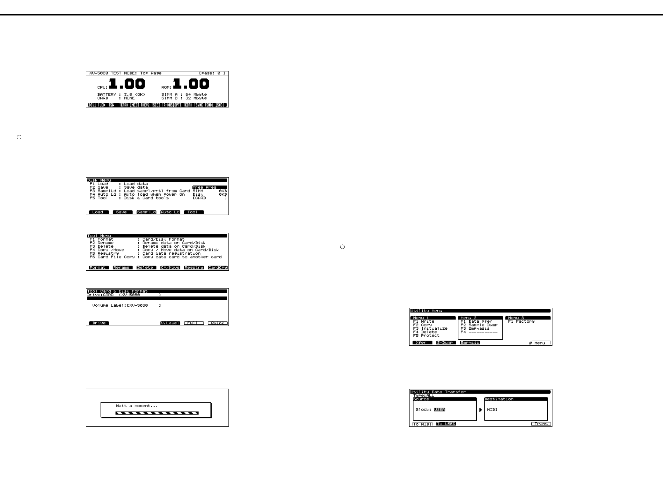
IDENTIFYING THE VERSION NUMBER
1. Turn on the power while pressing [EXIT].
2. Pressing [PHARASE PREVIEW] (VOLUME) while the opening mes-
sage is displayed enables TEST MODE where the Top pageappears.
The version numbers of the CPU and ROM will appear on the display.
*fig_ver1
SAVING AND LOADING THE USER DATA
Using the SmartMedia
* Before beginning the operation, format the SmartMedia.
• Formatting Procedure
1. Insert the SmartMedia in the memory card slot.
2. Press [DISK].
*fig_svld1
3. Press [F5](Tool).
*fig_svld2
バージョンナンバーの確認方法
バージョンナンバーの確認方法
バージョンナンバーの確認方法バージョンナンバーの確認方法
1. [EXIT] を押しながら電源を入れます。
2. 更に、オープニング・メッセージ表示中に [PHRASE PREVIEW]
(VOLUME) を押すとテストモードのトップページになります。
ここで CPU,ROM それぞれのバージョンが表示されます。
ユーザーデータのセーブとロード
ユーザーデータのセーブとロード
ユーザーデータのセーブとロードユーザーデータのセーブとロード
◯
スマートメディアを使用する場合
スマートメディアを使用する場合
スマートメディアを使用する場合スマートメディアを使用する場合
※作業を開始する前に、スマートメディアのフォーマットを行ってください。
・・・・ フォーマットの方法
フォーマットの方法
フォーマットの方法フォーマットの方法
1. スマートメディアをメモリーカードスロットに挿し込みます。
2. [DISK] を押します。
3. [F5](Tool) を押します。
• Saving the User Data
1. Check that the SmartMedia is inserted in the memory card slot.
2. Press [DISK].
3. Press [F2](Save).
4. Press [F1] (Drive).
5. Press the cursor key to select "CARD".
6. Press [F6](OK).
7. Press [F6](Save).The Save File window will appear.
Here, give the file a name.
8. Press [F6](OK). The message ”Save, OK?” appears.
9. When you press [F6](OK), the particular file was saved.
* If a file with the same name has already been written on the SmartMedia,
the program will ask you whether to overwrite it. To keep the oldfile, enter
a new file name and then save the file.
10.When the saving ends, the display will show return to showing the screen
in step3.
Pressing [DISK] causes the save screen to disapper.
• Loading the User Data
1. Check that the SmartMedia is inserted in the memory card slot.
2. Press [DISK].
3. Press [F1](Load).
4. Press [F1](Drive).
5. Press the cursor key to select "CARD".
6. Press [F6](OK).
7. Move the cursor to the file (.SVD) to be loaded and press [F6](Select).
8. When you press [F6](Load), press [F6] (OK) again, the particular file was
saved are loaded.
9. When the loading ends, the display will show return to showing the
screen in step3.
Pressing [DISK] causes the load screen to disapper.
・・・・ ユーザーデータのセーブ
ユーザーデータのセーブ
ユーザーデータのセーブユーザーデータのセーブ
1. スマートメディアがメモリーカードスロットに挿し込まれていることを
確認します。
2. [DISK] を押します。
3. [F2](Save) を押します。
4. [F1](Drive) を押します。
5. カーソルキーで、「CARD」を選びます。
6. [F6](OK) を押します。
7. [F6](Save) を押すと、Save File ウィンドウが表示されます。ここで
ファイル名をつけます。
8. [F6](OK) を押すと、「Save OK?」というメッセージが表示されます。
9. [F6](OK) を押すとセーブが実行されます。
※ スマートメディアに、すでに同名のファイルが書き込まれているときに
は、上書きをして良いかを聞いてきます。
元のファイルを保存しておきたいときには、新たなファイル名を入力し
てからセーブを行ってください。
10.セーブが終わると、3. の画面に戻ります。[DISK] を押すと、DISK の画
面から抜けます。
・・・・ ユーザーデータのロード
ユーザーデータのロード
ユーザーデータのロードユーザーデータのロード
1. スマートメディアがメモリーカードスロットに挿し込まれていることを
確認します。
2. [DISK] を押します。
3. [F1](Load) を押します。
4. [F1](Drive) を押します。
5. カーソルキーで、「CARD」を選びます。
6. [F6](OK) を押します。
カーソルキーでロードするファイル名を選択し、[F6](Select) を押します。
7.
8. [F6](Load) を押して、もう一度 [F6](OK) を押すと、データロードが行
われます。
9. ロードが終わると、3. の画面に戻ります。[DISK] を押すと、DISK の画
面から抜けます。
4. Press [F1](Format).
*fig_svld3
5. Press [F1](Drive).
6. Press the cursor key to select "CARD"
7. Press [F6](OK).
If desired, you can change the Volume Label by pressing
•
[F4](V.Label).
Press [F5](Full) or [F6](Quick), the program will ask you whether to format it.
8.
9. When you press [F6 (OK)], the format is executed.
*fig_svld4
4. [F1](Format) を押します。
5. [F1](Drive) を押します。
6. カーソルキーで、「CARD」を選びます。
7. [F6](OK) を押します。
・ ボリュームラベルを変更したい場合は、[F4](V.Label) を押すと、
ボリュームラベルの変更ができます。
8. [F5](Full) 又は [F6](Quick) を押すと、フォーマットして良いかを
聞いてきます。
9. [F6](OK) を押すとフォーマットが実行されます。
Bulk Dump Procedure
Items Required:
MIDI cable
•
Sequencer (Recordable)
•
• Saving the User Data
1.
Connect the MIDI OUT terminal of the XV-5080 to MIDI IN terminal of the
sequencer with a MIDI cable.
2. Press [SYSTEM/UTILITY] two times.
*fig_svld5
3. Press [F6](Menu) to select Menu 2. Press [F1](Data Xfer).
4. Press [F1](to MIDI)
5. Set the setting to Type = ALL, Block = USER.
6. Begin recording with the sequencer.
7. Press [F6](Trans) to begin the transfer of data.
*fig_svld6
◯
バルクダンプで行う場合
バルクダンプで行う場合
バルクダンプで行う場合バルクダンプで行う場合
準備するもの
・ MIDI ケーブル
・ シーケンサー(録音可能なもの)
・・・・ ユーザーデータのセーブ
ユーザーデータのセーブ
ユーザーデータのセーブユーザーデータのセーブ
1. XV-5080 の MIDI OUT 端子と、シーケンサーの MIDI IN を MIDI ケーブ
ルで接続します。
2. [SYSTEM/UTILITY] 2 回を押して、インジケーターを点滅させます。
[F6](Menu) を押して「Menu 2」を選び、[F1](Data Xfer) を押します。
3.
4. [F1](to MIDI) を押します。
5. 設定を Type = ALL、Block = USER に設定します。
6. シーケンサーの録音を開始します。
7. [F6](Trans) を押すと、データの転送が実行されます。
10.When the formatting ends, the display will show the message “Format
Completed!” and press [F6](Accept), the display will return to showing
the screen in step4.
Pressing [DISK] causes the format screen to disapper.
8
10.フォーマットが終わると、「Format Completed!」と表示され、
[F6](Accept) を押すと、4. の画面に戻ります。
[DISK] を押すと、DISK の画面から抜けます。
• Loading the User Data
1. Connect the MIDI IN terminal of the XV-5080 to the MIDI OUT terminal of
the sequencer with a MIDI cable.
2. Send the bulk dump from the sequencer.
・・・・ ユーザーデータのロード
ユーザーデータのロード
ユーザーデータのロードユーザーデータのロード
1. XV-5080 の MIDI IN 端子と、シーケンサーの MIDI OUT 端子をケーブル
でつなげます。
2. シーケンサーからバルクダンプを送信します。
Page 9
JUN. 2000 XV-5080
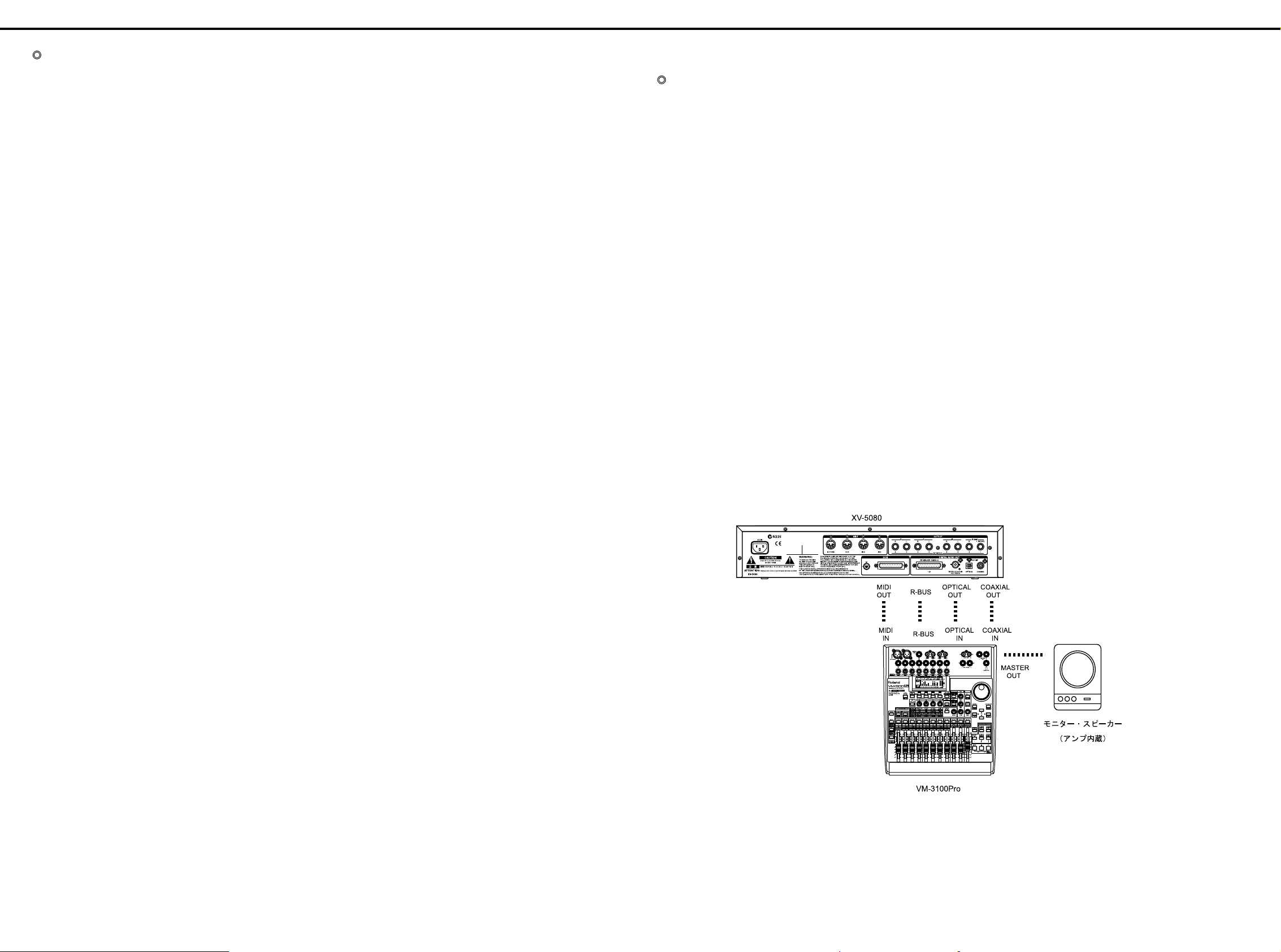
FACTORY RESET
1. Press [SYSTEM/UTILITY] two times.
*fig_fact1
2. Press the [F6](Menu), and select "Menu 3". Then press [F1](Factory).
*fig_fact2
3. The program will ask you whether to factory reset and then press
[F6](Factory).
If Internal Write Protect is ON, a warning will be issued and then the
•
display will show the following screen.
Press [DEC] to turn Internal Write Protect OFF.
*fig_fact3
ファクトリーリセットの方法
ファクトリーリセットの方法
ファクトリーリセットの方法ファクトリーリセットの方法
1. [SYSTEM/UTILITY] を 2 回押します。
2. [F6](Menu) を押して、「Menu 3」を選び、[F1](Factory) を押します。
3. ファクトリーリセットしても良いか聞いてくるので、[F6](Factory) を
押します。
・
Internal Write Protect が ON の場合、以下の画面が表示されます。
[DEC] を押して Internal Write Protect を OFF にします。
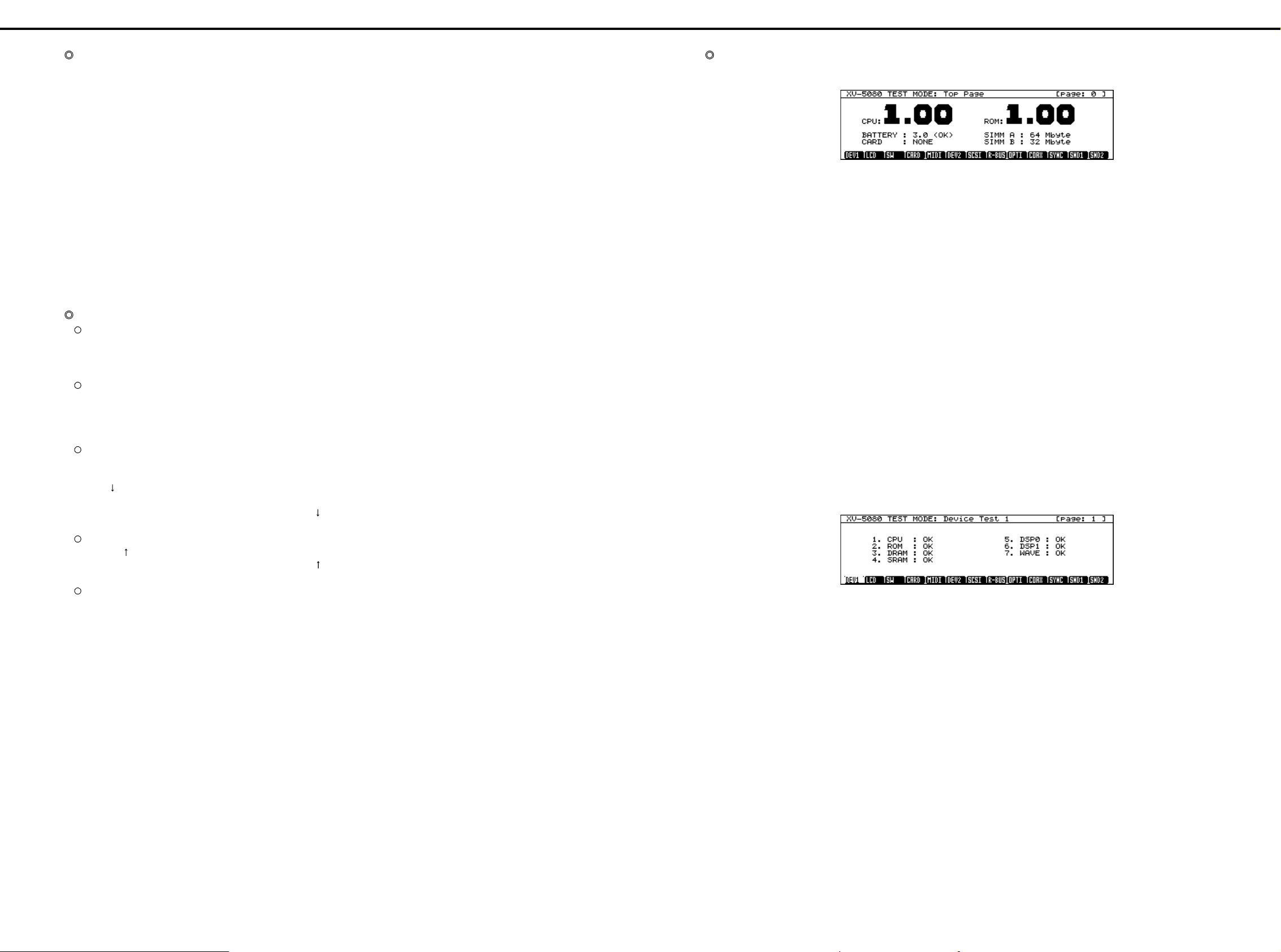
VERSION UP
The XV-5080 uses a flash memory for the program ROM. The version of
the program ROM can be upgraded by loading MIDI data into the XV-5080.
After upgrading the version, factory reset must be performed. If important
data is written in the user memory, save the data on a card before
upgrading the version.
Required Items:
XV-5080 Ver. Up Disk (2DD: Two disks)(17048561)
•
Sequencer capable of regenerating SMF (Also possible using a syn-
•
thesizer with a sequencer)
MIDI cable
•
Version Up Procedure
1. Connect the MIDI cable from MIDI OUT of the external sequencer to
MIDI IN of the XV-5080.
2. Turn on the XV-5080 power while holding down [DEC] and [A] at the
same time, and the display will show the following MIDI update screen.
*fig_update1
バージョンアップの方法
バージョンアップの方法
バージョンアップの方法バージョンアップの方法
XV-5080 は、プログラム ROM にフラッシュメモリを使用しています。
これは外部から MIDI データを送り込むことによりバージョンアップでき
ます。なお、バージョンアップ後は必ずファクトリーリセットを行う必要
があります。ユーザーメモリに大切なデータが書込まれている場合は、ス
マートメディアに保存してからバージョンアップ作業を行なって下さい。
◎用意するもの
◎用意するもの
◎用意するもの◎用意するもの
・ XV-5080 Ver.Up Disk (2DD:2 枚組)(17048561)
・ SMF の再生できるシーケンサー (XP-80 等のシーケンサー付きシン
セサイザーでも可)
・ MIDI ケーブル
◎バージョンアップの方法
◎バージョンアップの方法
◎バージョンアップの方法◎バージョンアップの方法
1. MIDIケーブルを外部シーケンサーの MIDI OUT から XV-5080 の MIDI
IN に接続します。
シーケンサーで SMF をチェインプレイできるように設定します。
2. [DEC] と [A] を同時に押しながら電源を入れると、以下のような
MIDI アップデート画面に入ります。
Press [F6](OK), and the display will return to showing the screen in step 2.
Press [F6](Factory), and perform factory reset.
*fig_fact4
4. Factory reset is performed, the display will show the message "COM-
PLETE" and automatically return to showing the original screen.
[F6](OK) を押すと、2 の画面に戻ります。
[F6](Factory) を押して、ファクトリーリセットを実行します。
4. ファクトリーリセットが終わると、「COMPLETE」を表示し、自動的に元
の画面に戻ります。
3. Press [INC], and the display will show the following screen, waiting for
the reception of MIDI data.
*fig_update2
4.
After confirming the display in step 3, regenerate all the ".mid" files in the
XV-5080 Ver. Up Disks 1 and 2 f rom the external sequencer (the order does
not matter). During the reception of MIDI data, the "MIDI message" LED
blinks and the message "Waiting" changes to the message "Recieving."
When the data transfer of one file ends, the message "Waiting" will
appear on the display. Then regenerate the next file.
The use of a sequencer with a chain play function, such as the XP-80,
allows the version to be upgraded even more easily. Load and play the
".svc" file (chain file), and all the ".mid" files found on Disk 1 will be
auto-matically regenerated. When regenerating Disk 1 all ends,
replace with Disk 2 and play it again.
5. When the update ends normally, the display will show the following
screen and the [A] to [H] LED's will blink.
*fig_update3
[INC] を押すと次の表示になり、MIDI データの受信待ち状態になります。
3.
4. 3. の表示を確認した後、XV-5080 Ver.Up Disk 1,2 の中にある全ての
".mid" ファイルを外部シーケンサから再生します。(順序は問いませ
ん)MIDI データ受信中は [MIDI message] の LED が点滅し、
「Waiting」の表示が「Recieving」に変わります。1 つのファイルの
データ転送が終了すると、表示が「Waiting」になりますので、続け
て次のファイルを再生して下さい。
なお、XP-80 等のチェインプレイ機能を持つシーケンサーを用いる
と、より簡単にバージョンアップができます。Disk 1 の中にある
".svc" ファイル(チェインファイル)をロードし、PLAY す ると、
Disk 1の中の全ての ".mid" ファイルを自動的に再生します。
Disk 1の再生が全て終了したら、Disk 2 に入れ替えて再び PLAY します。
5. アップデートが正常に終了すると次の表示になり、[A] -- [H] の
LED が点滅します。
6. After playing all the ".mid" files on the two Ver. Up Disks, turn on the
XV-5080 power again to ensure that the version has been upgraded
correctly.
7. Lastly, perform factory reset.
This completes the version up.
6. 2 枚の Ver.Up Disk の全ての ".mid" ファイルをプレイし終わったら、
電源を立ち上げ直して、正しくバージョンアップされていることを確
認して下さい。
7. 最後にファクトリーリセットを行なって下さい。
以上でバージョンアップは終了です。
9
Page 10
XV-5080 JUN. 2000
NOTES:
Number of SMF's
One SMF is created for one block of flash memory.
•
Thirty-two SMF's, p00001.mid to p00032.mid, are created.
•
Some files may be omitted depending on the size of the program.
•
SMF is always created in p00032.mid because checksum data is
•
placed in it.
Ending the update
When p00032.mid has been received, it is judged that all the update
•
data has been received. Any block, which has not been updated at
this point of time, will be erased. This is performed to properly con-
trol the checksum data in the external ROM. Therefore, some blocks
only cannot be updated.
◎注意点
◎注意点
◎注意点◎注意点
SMF の数について
SMF の数について
SMF の数について SMF の数について
・ SMF は Flash Memory の 1 ブロックに対して、一つ作られます。
・ p00001.mid -- p00032.mid の 32 個の SMF が作られます。
プログラムのサイズによっては、途中のファイルが抜ける事があります。
・
・
p00032.mid にはチェックサムデータが置かれますので必ず作られます。
アップデートの終了について
アップデートの終了について
アップデートの終了について アップデートの終了について
・ p00032.mid を受信し終えると、全アップデートデータを受信した
と判断しています。 この時点でアップデートされなかったブロック
は消去します。 これは外 ROM のチェックサムデータを正しく管理
するためです。 従って一部のブロックのみをアップデートすること
はできません。
TEST MODE
Preparation
Audio cables: 1 to 8
•
MIDI cable: 1
•
SmartMedia: 3
•
(Not protected: one each for 5V and 3.3V
Protected: one for 5V or 3.3V)
Monitor speaker (e.g. MA-12)
•
Headphone
•
Oscilloscope
•
Wave expansion board, SR-JV80 Series: 4
•
Wave expansion board, SRX Series: 4
•
SIMMs: 2
•
VM-3100Pro or the following equipments.
•
Equipment that accepts digital audio signals from the R-BUS.
Equipment that accepts digital audio signals from the coaxial lines.
Equipment that accepts digital audio signals from the optical lines.
R-BUS cable
•
COAXIAL cable
•
OPTICAL cable
•
SCSI-type ZIP drive
•
Oscillator
•
Caution: Since entering the Test mode may erase the user data,.always
back up the data before doing so.
Caution: Conducting the card test causes the contents of the Smartme-
dia card to be lost. So prepare and use a dedicated card for the
test.
Note: Mount the wave expansion board and SIMM on the unit before
turning the power on.
Mounting them with the power on may damage the board.
Note: Initialize the VM-3100Pro before testing.
Note: Connect the VM-3100Pro and the ZIP drive to the R-BUS and
SCSI, respectively, and turn the power on before testing.
* When testing the R-BUS,Optical, and Coaxial interfaces, connect the XV-
5080 and the VM-3100Pro as shown on the figure below:
*fig_test1
テストモード
テストモード
テストモードテストモード
◎準備するもの
◎準備するもの
◎準備するもの◎準備するもの
・ オーディオケーブル 1 ~ 8 本
・ MIDI ケーブル 1 本
・ スマートメディア 3 枚
(プロテクトされていないもの、5V 品、3.3V 品 各 1 枚ずつ。プロテ
クトされているもの 1枚。5V、3.3V どちらでも良い)
・ モニタースピーカー (MA-12 等 )
・ ヘッドホン
・ オシロスコープ
・ ウェーブエクスパンションボード SR-JV80 シリーズ 4 枚
・ ウェーブエクスパンションボード SRX シリーズ 4 枚
・ SIMM 2 枚
・ VM-3100Pro もしくは、以下の機器
R-BUS からデジタルオーディオ信号を入力できる機器
Optical からデジタルオーディオ信号を入力できる機器
Coaxial からデジタルオーディオ信号を入力できる機器
・ R-BUS ケーブル
・ COAXIAL ケーブル
・ OPTICAL ケーブル
・ SCSI 接続用の ZIP ドライブ
・発振機
テストモードに入るとユーザーデータは消去される場合があります。
注:
必ずデータのバックアップを行って下さい。
カードテストを行うと、スマートメディアの内容は失われてしまいます。
注:
テスト用のスマートメディアを準備し、使用して下さい。
注:ウェーブエクスパンションボード、SIMM は電源を入れる前にあら
かじめ本体に装着して下さい。
電源を入れたまま装着すると、ボードが壊れる可能性があります。
注:VM-3100Pro はあらかじめ初期化しておいてください。
注:VM-3100Pro、ZIP ドライブは、テストモードに入る前に R-BUS、
SCSI それぞれの接続をして、電源を入れておいて下さい。
※ R-BUS、Optical、Coaxial のテストでは、XV-5080 と VM-3100Pro とを
以下の図のように接続して下さい。
10
Page 11
JUN. 2000 XV-5080
Tests
The tests to be done on the XV-5080 are as listed below. Detailed procedures for each test are explained in the corresponding sections.
0 : Top Page
(Identifying the version number, battery check, memory card check)
1 : Device Test 1
2 : LCD&Encoder Test
3 : Switch&LED Test
4 : Card Test
5 : MIDI Test
6 : Device Test 2
7 : SCSI Test
8 : Digital/R-BUS Test
9 : Digital/Optical Test
10 : Digital/Coaxial Test
11 : Digital/Sync Test
12 : Sound Test 1
13 : Sound Test 2
14 : Factory Reset
Operation of Buttons
How to Enter the Test Mode
1) Turn on the power while pressing [EXIT].
2) Press [PHRASE PREVIEW] while the opening message is displayed, and the top page will appear.
How to Exit the Test Mode
Press [EXIT] in each test mode to return to the top page.
* In the Switch&LED test mode, however, press both the [SHIFT] and
] buttons simultaneously.
[
EXIT
Press [EXIT] on the top page to exit the Test mode.
How to Move to the Next Test
When a test is completed successfully, the system will bring you to the
next test automatically.
Press [ ] in a current test to move to the next text even if the current
test is not over yet.
* In the Switch&LED test mode, however, press both the [SHIFT] and [ ]
buttons simultaneously.
How to Return to the Previous Test
Press the [ ] cursor to return to the last test.
* In the Switch&LED test mode, however, press both the [SHIFT] and [ ]
buttons simultaneously.
How to Jump to a Test Mode
You can go to the test you want directly by selecting from [1/9] to [8/16]
and [PART SELECT] while pressing [SHIFT].
[SHIFT] + [1/17] 1. Device Test 1
[SHIFT] + [2/18] 2. LCD&Encoder Test
[SHIFT] + [3/19] 3. Switch&LED Test
[SHIFT] + [4/20] 4. Card Test
[SHIFT] + [5/21] 5. MIDI Test
[SHIFT] + [6/22] 6. Device Test 2
[SHIFT] + [7/23] 7. SCSI Test
[SHIFT] + [8/24] 8. Digital/R-BUS Test
[SHIFT] + [9/25] 9. Digital/Optical Test
[SHIFT] + [10/26] 10. Digital/Coaxial Test
[SHIFT] + [11/27] 11. Digital/Sync Test
[SHIFT] + [12/28] 12. Sound Test 1
[SHIFT] + [13/29] 13. Sound Test 2
[SHIFT] + [PART SELECT] 14. Factory Reset
◎テスト項目
◎テスト項目
◎テスト項目◎テスト項目
XV-5080 には以下のテストがあります。
各テストの詳細については、それぞれの項目を参照して下さい。
0 : Top Page
(Identifying the version number,Battery check,Memory cardcheck)
1 : Device Test 1
2 : LCD&Encoder Test
3 : Switch&LED Test
4 : Card Test
5 : MIDI Test
6 : Device Test 2
7 : SCSI Test
8 : Digital/R-BUS Test
9 : DIgital/Optical Test
10 : Digital/Coaxial Test
11 : Digital/Sync Test
12 : Sound Test 1
13 : Sound Test 2
14 : Factory Reset
◎ボタン操作
◎ボタン操作
◎ボタン操作◎ボタン操作
○ テストモードへの入り方
1) [EXIT] を押しながら電源を入れます。
2) 更に、オープニング・メッセージ表示中に [PHRASE PREVIEW] を
押すとテストモードのトップページになります。
○ テストモードからの抜け方
各テスト項目で、[EXIT] を押すと、トップページに戻ります。
※但し、Switch&LED test では [SHIFT] と [EXIT] の2つのボタンを押し
ます。
トップページで [EXIT] 押すと、テストモードを抜けます。
○ 次のテストに移る
テストが正常に終了すると自動的に次のテスト項目へ移動します。
カーソル [ ↓ ] を押すと、テストが終了していなくても次のテスト
項目に移動します。
※但し、Switch&LED test では [SHIFT] と カーソル [ ↓ ] の2つのボタ
ンを押します。
○前のテストに戻る
カーソル [ ↑ ] を押すと一つ前のテスト項目に移動します。
※但し、Switch&LED test では [SHIFT] と カーソル [ ↑ ] の2つのボタ
ンを押します。
○ 各テストへのジャンプ
[SHIFT] を押しながら [1/9] ~ [8/16],[PART SELECT] を押すと対応
するテスト項目を直接選択できます。
[SHIFT] + [1/17] 1. Device Test 1
[SHIFT] + [2/18] 2. LCD&Encoder Test
[SHIFT] + [3/19] 3. Switch&LED Test
[SHIFT] + [4/20] 4. Card Test
[SHIFT] + [5/21] 5. MIDI Test
[SHIFT] + [6/22] 6. Device Test 2
[SHIFT] + [7/23] 7. SCSI Test
[SHIFT] + [8/24] 8. Digital/R-BUS Test
[SHIFT] + [9/25] 9. Digital/Optical Test
[SHIFT] + [10/26] 10. Digital/Coaxial Test
[SHIFT] + [11/27] 11. Digital/Sync Test
[SHIFT] + [12/28] 12. Sound Test 1
[SHIFT] + [13/29] 13. Sound Test 2
[SHIFT] + [PART SELECT] 14. Factory Reset
Explanation of Tests Details
0 : Top Page
*fig_test2
Check the versions of the CPU and the Program ROM.
•
If the version is not current, update it.
Refer to "How to Update a Version" for how to do it.
Check the voltage of the SRAM battery.
•
Battery: OK : Voltage normal
NG : Voltage abnormal
* "OK" will be displayed if the battery voltage is 2.5V to 4.0V.
If "NG" is displayed, check BT1, IC2, IC9, and DA4 on the main board.
Check the status of the memory-card slot and the SmartMedia inserted.
•
NONE : No SmartMedia card is inserted.
PROTECTED : The SmartMedia card is protected.
NON-PROTECT : The SmartMedia card is not protected.
If the display is not correct, check Q16, IC66 and CN14 on the main board.
Check the capacity of the SIMMs inserted in SIMM slots A and B.
•
If the display is not correct, check CN13, CN14 and IC24 to 27 on
the EXP base board.
Check that you can adjust the contrast of the LCD by turning the
•
Encoder control.
If you cannot, check IC4 and IC11 on the main board.
If all the checks were completed successfully, press [VALUE] to pro-
•
ceed to the next test.
1 : Device Test 1
*fig_test3
CPU-RAM/ROM , Program ROM, DRAM, SRAM, XV-DSP/RAM
•
and Wave ROM are tested automatically.
1. CPU: OK : The RAM and ROM are operating normally.
NG : Abnormal. Check IC3 on the main board.
2. ROM: OK : The Program ROM is operating normally.
NG :
Abnormal. Check IC1,IC117 and IC106 on the main board.
3. DRAM: OK : The DRAM is operating normally.
NG :
Abnormal. Check IC117 and IC118 on the main board.
4. SRAM: OK : The SRAM is operating normally.
NG :
Abnormal. Check IC84 and IC6 on the main board.
5. DSP0: OK :
I0-NG : The internal RAM of XV0 is abnormal. Check IC13
E0-NG : The external RAM of XV0 is abnormal. Check
6. DSP1: OK :
I1-NG : The internal RAM of XV1 is abnormal. Check IC12
E1-NG : The external RAM of XV1 is abnormal. Check
7. Wave: OK : The Wave ROM is operating normally.
NG :
Both the DSP and RAM of XV0 are operating normally.
on the main board.
IC19 on the main board.
Both DSP and RAM of XV1 are operating normally.
on the main board.
IC18 on the main board.
Abnormal. Check IC26 and IC29 on the main board.
◎テスト項目詳細
◎テスト項目詳細
◎テスト項目詳細◎テスト項目詳細
0 : Top Page
・ CPU, Program ROM のバージョンを確認します。
バージョンが適切でない場合は、バージョンアップを行って下さい。
アップデートの方法については、「バージョンアップの方法」を参
照して下さい。
・ SRAM 用 バッテリー の電圧を確認します
Battery: OK 正常な電圧です。
NG 異常な電圧です。
※ バッテリー電圧が 2.5V ~ 4.0V の場合 OK になります。
NG の場合はメインボードの BT1,IC2,IC9,DA4 をチェックしてください。
・ メモリーカードスロットと挿入したスマートメディアの状態を確
認します。
NONE スマートメディアが挿入されていません。
PROTECTED スマートメディアはプロテクトされています。
NON-PROTECT スマートメディアはプロテクトされていません。
表示が正しくない場合は、メインボードの Q16,IC66,CN14 を
チェックして下さい。
SIMM スロット A,B に挿入されている SIMM の容量をそれぞれ確認します。
・
容量の表示が正しくない場合は、EXP ベースボード
CN13,CN14,IC24 ~ 27 をチェックして下さい。
・
Encoder を回すと LCD コントラストの調整ができることを確認します。
調整ができない場合はメインボードの IC4,IC11 をチェックして下さい。
・ 全て確認したら [VALUE] を押し、次のテストに進みます。
1 : Device Test 1
・ CPU-RAM/ROM , Program ROM , DRAM ,SRAM ,XV-DSP/RAM ,Wave ROM
を自動的にチェックします。
1. CPU: OK CPU の RAM と ROM は正常です。
NG
異常です。メインボードの IC3 をチェックして下さい。
2. ROM: OK Program ROM は正常です。
NG 異常です。メインボードの IC1,IC117,IC106 をチェッ
クして下さい。
3. DRAM: OK DRAM は正常です。
異常です。メインボードの IC117,IC118 をチェックして下さい。
NG
4. SRAM: OK SRAM は正常です。
異常です。メインボードの IC84,IC6 をチェックして下さい。
NG
5. DSP0: OK XV0 の DSP と RAM はすべて正常です。
I0-NG XV0 の内部 RAM が異常です。メインボードの IC13 を
チェックして下さい。
E0-NG XV0 の外部 RAM が異常です。メインボードの IC19 を
チェックして下さい。
6. DSP1:OK XV1のDSP と RAM はすべて正常です。
I1-NG XV1の内部 RAM が異常です。メインボードの IC12 を
チェックして下さい。
E1-NG V1の外部RAM が異常です。メインボードの IC18 を
チェックして下さい。
7. Wave: OK Wave ROM は正常です。
異常です。メインボードの IC26,IC29 をチェックして下さい。
NG
11
Page 12
XV-5080 JUN. 2000
If all the checks are completed successfully, the system will move on
•
to the next test automatically.
2 : LCD&Encoder Test
*fig_test4
Confirm that you can adjust the contrast of the LCD by turning the
•
Encoder control. Confirm that changing the contrast value causes
the LED number to light up.
Confirm that pressing [VALUE] for the first time causes all the LCD
•
dots to light up.
Confirm that pressing [VALUE] for the second time causes all the
•
LCD dots to go off.
Confirm that pressing [VALUE] for the third time causes a pattern to
•
be displayed.
Confirm that pressing [VALUE] for the forth time causes the pattern
•
to appear in reverse video.
If any of the tests listed above fail, check IC4, IC51, RA70 and RA71
on the main board.
Pressing [VALUE] for the fifth time will bring you to the next test.
•
3 : Switch&LED Test
*fig_test5
・すべてが OK ならば、自動的に次のテスト項目に移ります。
2 : LCD&Encoder Test
・
Encoder を回すと LCD コントラストが調整できることを確認します。
LCD コントラストの値に応じて LED 点灯個数が変化することを確
認します。
・ [VALUE](1回目)を押すと LCD の全ドットが点灯することを確認
します。
・ [VALUE](2回目)を押すと LCD の全ドットが消灯することを確認
します。
[VALUE](3回目)を押すと、パターンが表示されることを確認します。
・
・ [VALUE](4回目)を押すと、パターンが反転表示されることを確
認します。
コントラストの調整、全消灯、全点灯、パターン表示ができない
場合、メインボード IC4,IC51,RA70,RA71 をチェックしま す。
・ [VALUE](5回目)を押すと、次のテスト項目になります。
3 : Switch&LED Test
Change the inserted card with the protected one, and press [PATCH
•
FINDER].
Confirm that the Card Status display changes to [PROTECTED].
The system will display "OK" to the right of "Card Status" after recog-
•
nizing both [PROTECTED] and [NON-PROTECT].
OK : Operating normally
•
WRITE-ERR : Write failed
•
READ-ERR : Read failed
•
CARD-ERR : Inserted SmartMedia is not correct.
•
* Unprotected SmartMedia cards are used in Read/Write Test 1 and 2.
If a WRITE-ERR or READ-ERR occurs, check CN6 and 7 on the media
board, as well as IC62, IC103 and IC104 on the main board.
If all the checks are "OK", the system will move on to the next test
•
automatically.
Caution: If the SmartMedia card was inserted or removed while data was
being read or written to it, the card may be damaged. ("Card
Status [UNFORMAT]" will be displayed.)
In this case, reformat the card and resume the test.
Press [SYSTEM/UTILITY] in this test to bring up the format
screen.
Press [VALUE] to format the card. After formatting, the display will
•
return to the card test.
If formatting fails, "Error!" will be displayed. Try reformatting, or use
•
another card.
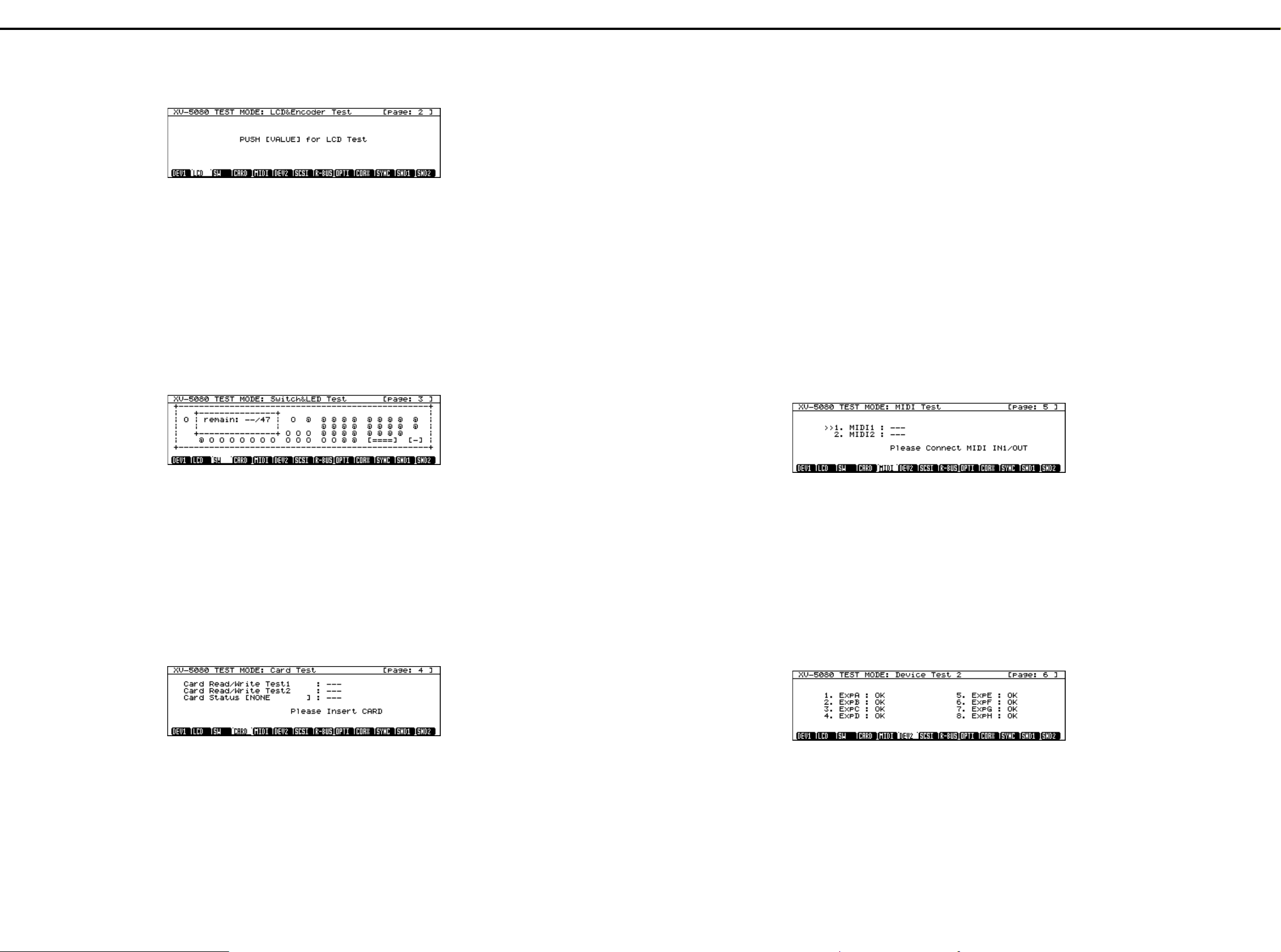
5 : MIDI Test
*fig_test7
・ プロテクトしてあるスマートメディアと交換し、[PATCH FINDER] を
押します。
Card Status [PROTECTED] の表示を確認します。
・ [PROTECTED]、[NON-PROTECT] の両方を認識すると、Card Status の
右の項目に OK を表示します。
・ OK : 正常です
・ WRITE-ERR : 書き込み失敗です
・ READ-ERR : 読み込み失敗です
・ CARD-ERR : 適切なスマートメディアが挿入されていません。
※ Read/Write Test1,2 は、プロテクトしていないスマートメディアで行
います。
WRITE-ERR,READ-ERR の場合は、メディアボードの CN6,7、メインボード
の IC62,IC103,IC104 をチェックして下さい。
・すべて OK になると、自動的に次のテスト項目に移ります。
注:スマートメディアの出し入れをする際に、データの読み書きが行わ
れた場合、スマートメディアが壊れてしまうことがあります。
(Card Status [UNFORMAT] の表示になります。)
このときは、スマートメディアをフォーマットし直して、再度この
テストを行って下さい。
このテスト項目中に、[SYSTEM/UTILITY] を押すと、フォーマット
の画面になります。
・ [VALUE] を押すとフォーマットすることが出来ます。フォーマット終
了後、Card Test の項目に戻ります。
・ フォーマットに失敗すると、"Error!" を表示します。再度フォー
マットをしてみるか、カードを取り替えてください。
5 : MIDI Test
Confirm that all the LEDs are lit.
•
Press the switches one by one. The LED will go off when the switch
•
with an LED is pressed, and the display will change from "0" to ".".
If a switch without an LED is pressed, the display will change from
"@" to "X".
Note: Pressing more than one switch simultaneously has no effect.
The display "remain: **/47" shows the number of the switches not
•
yet pressed. (** stands for such number.)
If the LED does not turn on or off, or the display is not correct, check
LED, SW and DA on the panel board, as well as IC57, IC58, Q3 to
14, CN11 and CN19 on the main board.
When "remain" reaches "0", "Complete!" will be displayed, and the
•
next test mode entered.
4 : Card Test
*fig_test6
Caution:
Conducting this test causes, the contents of the SmartMedia to
be lost. So prepare and use a dedicated card for the test.
Insert an unprotected SmartMedia (for 5V or 3.3V) into the card slot,
•
and press [PATCH FINDER].
Confirm that the Card Status display changes to [NON-PROTECT],
and that "OK" is displayed for "Card Read/Write test1".
Insert another unprotected card into the card slot, and press
•
[PATCH FINDER].
Confirm that the Card Status display changes to [NON-PROTECT],
and that "OK" is displayed for "Card Read/Write test2".
・すべての LED が点灯していることを確認します。
・ スイッチを押していくと、LED 付きのスイッチは LED が消灯し、画
面の対応するスイッチの表示は " 0 " → "." に変わります。
LED のないスイッチを押すと、画面のスイッチの表示は " @ " →
" × " に変わります。
注:複数のスイッチを同時に押した場合は無効です。
・まだ押されていないスイッチの個数が remain: 個数 /47 として表
示されます。
LED が点灯、消灯しない、またはディスプレイの表示が正しくない
場合、パネルボードの各 LED,SW,DA, メインボードの IC57,IC58,Q3
~ 14,CN11,CN19 をチェックして下さい。
・ remain が 0 になると、"Complete!" と表示して次のテストモード
に移ります。
4 : Card Test
注:このテストを行うと、スマートメディアの内容は失われてしまい
ます。テスト用のスマートメディアを準備し、使用して下さい。
・ プロテクトしていないスマートメディア (5V 又は 3.3V どちらか一
方)をカードスロットに挿入し、[PATCH FINDER] を押します。
Caed Status が [NON-PROTECT] の表示になり、Card Read/Write
test1 が OK となることを確認します。
・ プロテクトしていないスマートメディアの、もう 1 枚を挿入し、
[PATCH FINDER] を押します。
Caed Status が [NON-PROTECT] の表示になり、Card Read/Write
test2 が OK となることを確認します。
Connect MIDI IN 1 and MIDI OUT using a MIDI cable.
•
If a MIDI cable is already connected to the VM-3100Pro, change the
connection only during this test.
Confirm that "MIDI 1" is displayed "OK".
Change the MIDI cable connection to MIDI IN 1 to MIDI IN 2.
•
Confirm that "OK"is displayed for "MIDI 2".
If any of the displays are not correct, check IC35 and IC36 on the EXP
base board.
Removing the MIDI cable will bring you to the next test.
•
If you want to proceed with the test in order, reconnect the MIDI cable
to the VM-3100Pro.
6 : Device Test 2
*fig_test8
In device test 2, the expansion board slots are tested.
•
This test requires that all slots be mounted with expansion boards.
If you mount the boards at this time, turn off the power first, mount the
boards, and resume the test mode.
If you mount the boards with the power on they may be damaged.
・ MIDI IN 1 と MIDI OUT を MIDI ケーブルで接続します。
MIDI ケーブルが VM-3100Pro に接続してある場合は、このテスト項目
のときだけ、接続しなおしてください。
MIDI 1 が OK と表示されることを確認します。
・ MIDI ケーブルを MIDI IN 1 から MIDI IN 2 につなぎ変えます。
MIDI 2 が OK と表示されることを確認します。
表示が正しくない場合は、EXP ベースボードの IC35,IC36 をチェック
して下さい。
・ MIDI ケーブルを抜くと、自動的に次のテスト項目に移ります。
テストを順に進める場合は、MIDI ケーブルを VM-3100Pro に接続しな
おしてください。
6 : Device Test 2
・ エクスパンションボードのスロットのテストを行います。
この項目に入る前に エクスパンションボードをすべてのスロットに
装着しておく必要があります。
この時点でエクスパンションボードを装着する場合は、一度電源を
切ってボードを装着し、再度テストモードに入ってください。
電源を入れたまま装着すると、ボードが壊れる可能性があります。
12
Page 13

JUN. 2000 XV-5080
Each slot is checked automatically.
•
A/B/C/D/E/F/G/H : OK : Operating normally
NG : Abnormal
If "NG" occurs, check the following depending on the slot:
A,B,C,or D : IC1 to 7 on the EXP base board
E,F,G, or H : IC8 to 17 on the EXP base board
If all the slots are "OK", the system will move on to the next test auto-
•
matically.
7 : SCSI Test
fig_test9
Connect the ZIP drive to SCSI.
•
Confirm that the ZIP drive is powered on.
•
Turning the SCSI ID Switch changes the ID number, and "-" displays
•
the number selected.
Change the number from 0 through 7, and confirm that the numbers
are displayed.
Turning the VALUE control starts the Read/Write test.
•
DEV-NOT-FOUND : No device found
•
DISK-NOT-FOUND : No disk found
•
MEM-ERR : Memory abnormal
•
READ-ERR : Read failed
•
WRITE-ERR : Write failed
•
COMPARE-ERR : Compare failed
•
If an error is displayed, check IC3, IC4, IC53 and IC56.
If DEV-NOT-FOUND is displayed, check the SCSI cable connection
and CN9 on the main board.
* In the Test mode, the SCSI ID of the machine being tested is set at "7"
inrespective of the SW setting.
* Set the SCSI ID on the ZIP side at 5 or 6.
If the Read/Write test was "OK", the system will proceed to the next test.
•
8 : Digital/R-BUS Test
In tests 8 through 10, procedures are described for both cases where the
VM-3100pro is used and not used.
TheVM-3100pro, which sends MIDI signals, performs tests 8 through 10
automatically. When the VM-3100pro is used before starting this test,
check the connection to the VM-3100Pro.
If you connect the unit at this time, go back to the previous test first, connect the unit, and then enter this test again.
fig_test10
・各スロットを自動的にチェックします。
A/B/C/D/E/F/G/H : OK 正常です。
NG 異常です。
NG の場合、スロットによって以下の個所をチェックして下さい。
A,B,C,D いずれか : EXP ベースボードの IC1 ~ 7
E,F,G,H いずれか : EXP ベースボードの IC8 ~ 17
全てのスロットが OK になると、自動的に次のテスト項目に移ります。
・
7 : SCSI Test
・ ZIP ドライブを SCSI 接続します。
・ ZIP の電源が入っていることを確認します。
・ SCSI ID Switch を回して変化させると、- の表示が選択された番号
になります。
0 - 7 全てに変化させ、番号が表示されることを確認します。
・ VALUE を押すと Read/Write テストを開始します。
・ DEV-NOT-FOUND : デバイスがありません。
・ DISK-NOT-FOUND : ディスクがありません。
・ MEM-ERR : メモリ異常です。
・ READ-ERR : 読み込み失敗です。
・ WRITE-ERR : 書き込み失敗です。
・ COMPARE-ERR : 照合失敗です。
何れかのエラー表示が出た場合、IC3,IC4,IC53,IC56 をチェックして
下さい。
DEV-NOT-FOUND の時は、SCSI ケーブルの接続、メインボード CN9 も
チェックして下さい。
※ テストモードにおいては自機の SCSI ID は、SW 設定に関わらず 7 固定
で動作します。
※ ZIP 側の SCSI ID は 5,6 のいずれかに設定してください。
・ Read/Write テストが OK になると、次のテスト項目に移ります。
8 : Digital/R-BUS Test
M-3100Pro を使用する場合と、使用しない場合とに分けて記載します。
なお、VM-3100pro を用いると、MIDI 信号を送ることにより、自動的に
8 ~ 10 のテストを行うことができます。
VM-3100pro を使用し、このテストを行う場合は、テストに入る前に、
VM-3100Pro との接続を確認しておきます。
この時点で接続する場合は、一度前のテストに戻り、接続した後にこの
テストに入ってください。
Pressing [9/25] to [16/32] allows you to select the output destination
•
directly.
DONE : Output normally
•
IPC NG : Abnormal IPC found. Check IC107 on the main board.
•
If DONE is displayed and a defective sound is stilloutput, check
IC13, IC46 and CN8 on the main board.
After all the sounds are OK, press [VALUE] to proceed to the next test.
•
When the VM-3100 Pro is unavailable, use VM-7100, VM-7200,VSR880, ADA-7000 or other equipment that accepts digital audio signals
from the R-BUS. Take the following steps to test the R-BUS lines.
Using a R-BUS cable, connect the equipment with the XV-5080.
•
Connect the equipment with speakers or headphones.
•
Set the equipment so that it externally synchronizes with the R-BUS.
•
Press the [VALUE] and [9/25] through [16/32] keys to check that
•
sound is output from each output terminal.
9 : Digital/Optical Test
fig_test11
Repeat pressing [VALUE] to output the sounds in the following order:
•
1) OUTPUT A-L (sine wave)
2) OUTPUT A-R (sine wave)
"DONE" is displayed for the sound being output.
•
Pressing [9/25], [10/26] allows you to select the output destination directly.
•
If DONE is displayed and a defective sound is still output, check
IC38 and CN7.
After all the sounds are OK, press [VALUE] to proceed to the next test.
•
When the VM-3100Pro is unavailable, use VM-7100, VM-7200, VSR880, DS-90 or other equipment that accepts digital audio signals from
the optical lines. Take the following steps to test the digital/optical lines.
Using an optical cable, connect the optical input terminal on the
•
equipment with the XV-5080.
When the equipment is a mixer or recorder, connect speakers or
•
headphones.
Set the equipment so that it externally synchronizes with the optical line.
•
Press the [VALUE], [9/25] and [10/26] keys to check that sound is
•
output from each output terminal.
10 : Digital/Coaxial Test
fig_test12
・ [9/25] ~ [16/32] を押すと、出力先を直接選択できます。
・ DONE :出力は正常です。
・ IPC NG :IPC 異常が検知されました。メインボードの IC107 を
チェックして下さい。
DONE が表示されても、発音が正しくない場合は、メインボードの
IC13,IC46,CN8 をチェックして下さい。
・ 全て発音を行った後、[VALUE] を押すと次のテスト項目に移ります。
VM-3100Pro を準備できない場合は、R-BUS からのデジタルオーデ ィオ
信号を入力できる機器 (VM-7100、VM-7200、VSR-880、ADA-7000 等)
で以下の手順により R-BUS のテストを行ってください。
・ R-BUS を入力できる機器と XV-5080 を R-BUS ケーブルで接続します。
R-BUS を入力できる機器とスピーカー、又はヘッドホンを接続します。
・
・
R-BUS を入力できる機器を、R-BUS に外部同期するように設定します。
・ [VALUE]、[9/25] ~ [16/32] を押して、それぞれの出力先よりサウ
ンドが出力されるのを確認します。
9 : Digital/Optical Test
・ [VALUE] を押していくと、以下の順にサウンドが出力されます。
1) OUTPUT A-L ( サイン波 )
2) OUTPUT A-R ( サイン波 )
・ 発音した項目には DONE を表示します。
・ [9/25],[10/26] を押すと、出力先を直接選択できます。
発音が正しくない場合、IC38,CN7 をチェックして下さい。
全て発音を行った後、[VALUE] を押すと次のテスト項目に移ります。
・
VM-3100Pro を準備できない場合、Optical からのデジタルオーデ ィオ
信号を入力できる機器 (VM-7100、VM-7200、VSR-880、DS-90 等)で、
Digital/Optical のテストを行ってください。
・ Optical を入力できる機器の Optical 入力端子と、XV-5080 を
Optical ケーブルで接続します。
・ 準備した機器がミキサーやレコーダーの場合、スピーカー又は
ヘッドホンを接続します。
・
Optical を入力できる機器を、Optical に外部同期するように設定します。
・ [VALUE]、[9/25]、[10/26] を押して、それぞれの出力先よりサウ
ンドが出力されるのを確認します。
10 : Digital/Coaxial Test
Repeat pressing [VALUE] to output several types of sounds in the fol-
•
lowing order:
1) OUTPUT A-L (sine wave)
2) OUTPUT A-R (sine wave)
3) OUTPUT B-L (square wave)
4) OUTPUT B-R (square wave)
5) OUTPUT C-L (sawtooth wave)
6) OUTPUT C-R (sawtooth wave)
7) OUTPUT D-L (sine wave)
8) OUTPUT D-R (sine wave)
・ [VALUE] を押していくと、以下の順序でサウンドが出力されます。
1) OUTPUT A-L ( サイン波 )
2) OUTPUT A-R ( サイン波 )
3) OUTPUT B-L ( 方形波 )
4) OUTPUT B-R ( 方形波 )
5) OUTPUT C-L ( のこぎり波 )
6) OUTPUT C-R ( のこぎり波 )
7) OUTPUT D-L ( サイン波 )
8) OUTPUT D-R ( サイン波 )
Repeat pressing [VALUE] to output the sounds in the following order:
•
1) OUTPUT A-L (sine wave)
2) OUTPUT A-R (sine wave)
"DONE" is displayed for the sound being output.
•
Pressing [9/25], [10/26] allows you to select the output destination directly.
•
If DONE is displayed and a defective sound is still output, check
IC41 and FL1.
After all the sounds are OK, press [VALUE] to proceed to the next test.
•
When the VM-3100Pro is unavailable, use VM-7100, VM-7200, VSR880, DS-90 or other equipment that accepts digital audio signals from
the coaxial lines. Take the following steps to test the digital/coaxial lines.
Using a coaxial cable, connect the coaxial input terminal on the
•
equipment with the XV-5080.
When the equipment is a mixer or recorder, connect speakers or
•
headphones.
Set the equipment so that it externally synchronizes with the Coaxial line.
•
Press the [VALUE] and [9/25] through [10/26] keys to check that
•
sound is output from each output terminal.
・ [VALUE] を押していくと、以下の順にサウンドが出力されます。
1) OUTPUT A-L ( サイン波 )
2) OUTPUT A-R ( サイン波 )
・ 発音した項目には DONE を表示します。
・ [9/25],[10/26] を押すと、出力先を直接選択できます。
発音が正しくない場合、IC41,FL1 をチェックして下さい。
・ 全て発音を行った 後、[VALUE] を押すと次のテスト項目に移ります。
VM-3100Pro を準備できない場合、Coaxial からのオーディオ信号を入
力できる機器 (VM-7100、VM-7200、VSR-880、DS-90 等)で、Digital/
Coaxial のテストを行ってください。
・ Coaxial を入力できる機器の Coaxial 入力端子と、XV-5080 を
Coaxial ケーブルで接続します。
・ 準備した機器がミキサーやレコーダーの場合、スピーカー又は
ヘッドホンを接続します。
・
Coaxial を入力できる機器を、Coaxial に外部同期するように設定します。
・ [VALUE]、[9/25]、[10/26] を押して、それぞれの出力先よりサウ
ンドが出力されるのを確認します。
13
Page 14

XV-5080 JUN. 2000
11 : Digital/Sync Test
fig_test13
Connect an oscillator to the WORD CLOCK IN terminal.
•
Set the oscillator at 44.1kHz. The system will display "OK" after con-
•
firming sync, and output a sine wave sound from OUTPUT A-L.
Press VALUE.
•
Set the oscillator at 48.0kHz. The system will display "OK" after con-
•
firming sync, and output a sine wave sound from OUTPUT A-R.
* [ Hz] on the right upper section of the display shows the Clock input
status.
If "OK" is not displayed, check IC37, IC39 to 43, IC45, IC49, IC50 and IC113.
After all outputs are OK, press [VALUE] to proceed to the next test.
•
12 : Sound Test 1
*fig_test14
11 : Digital/Sync Test
・ WORD CLOCK IN 端子に発振機を接続します。
・発振機の設定を 44.1KHz とし、同期を確認すると OK を表示して
OUTPUT A-L より サイン波が発音されます。
・ ここで VALUE を押します。
・発振機の設定を 48.0KHz とし、同期を確認すると OK 表示して
OUTPUT A-R よりサイン波を発音します。
※右上の [ Hz] 内には、Clock 入力 の状態を表示しています。
OK が表示されない場合、IC37,IC39 ~ 43,IC45,IC49,IC50,IC113 を
チェックして下さい。
・全てOK の場合 [VALUE] を押して、次のテスト項目に移ります。
12 : Sound Test 1
After all the sounds are OK, press [VALUE] to proceed to the next test.
•
13 : Sound Test 2
*fig_test15
In this test, the sound is output from OUTPUT A and headphone L and R.
•
Confirm that the monitor speaker is connected correctly.
Pressing [VALUE] starts the test sounding.
•
Pressing [VALUE] again stops the test sounding and goes on to the
•
next text.
If no sound is output or stopped, check IC4, IC12 and IC13 on the
main board.
14 : Factory Reset
*fig_test16
全ての発音を行った後、[VALUE] を押すと次のテスト項目に移り ます。
・
13 : Sound Test 2
・ テスト発音は、OUTPUT A とヘッドホン L,R から出力されます。
モニタースピーカーの接続を確認してください。
・ [VALUE] を押すとテスト発音を開始します。
・もう1度 [VALUE] を押すとテスト発音を停止し、次のテスト項目に
移ります。
音が出力されない、または停止しない場合、メインボードの
IC4,IC12,IC13 をチェックして下さい。
14 : Factory Reset
Repeat pressing [VALUE] to output the sounds from each output ter-
•
minal in the following order:
Confirm the output sound with the monitor speaker or headphones.
* Sound is output from different terminals. Reconnect the audio cable as
required.
1) OUTPUT A-L & headphone L (sine wave)
2) OUTPUT A-R & headphone R (sine wave)
3) OUTPUT B-L (square wave)
4) OUTPUT B-R (square wave)
5) OUTPUT C-L (sawtooth wave)
6) OUTPUT C-R (sawtooth wave)
7) OUTPUT D-L (sine wave)
8) OUTPUT D-R (sine wave)
"DONE" is displayed for the output destination.
•
Pressing [9/25] to [16/32] allows you to select the output destination
•
directly.
If the sound is not output correctly, check the following points
depending on the destination:
No output : CN17,Q23 to 26,and IC76 on the main
OUTPUT A & headphone L,R
OUTPUT A : IC70 to 72 or the main board; IC1 on
OUTPUT A-L only : Q19,C233 and C220 on the main
OUTPUT A-R only : Q20,C245and C228 on the main board;
Headphone L,R : IC69 on the main board
Headphone L only : Q17 and C214 on the main board
Headphone R only : Q18 and C226 on the main board
OUTPUT B : IC73 to 75 on the main board
OUTPUT B-L only : Q21 and C253 on the main board
OUTPUT B-R only : Q22 and C259 on the main board
OUTPUT C : IC78 to 80 on the main board
OUTPUT C-L only : Q27 and C283 on the main board
OUTPUT C-R only : Q28 and C292 on the main board
OUTPUT D : IC81 to 83 on the main board
OUTPUT D-L only : Q29 and C308 on the main board
OUTPUT D-R : Q29 and C317 on the main board
board
: CN16,IC70,and IC71 on the main
board; CN5 of the phones board
the phones board
board; C3 of the phones board
C7 of the phones board
・ [VALUE] を押していくと各出力端子に以下の順序でサウンドが出力
されます。
出力される音をモニタースピーカーとヘッドホンで確認します。
※出力される端子が それそ れ異なるので、適宜オーディオケーブルを
接続し直してください。
1) OUTPUT A-L & ヘッドホン L ( サイン波 )
2) OUTPUT A-R & ヘッドホン R ( サイン波 )
3) OUTPUT B-L ( 方形波 )
4) OUTPUT B-R ( 方形波 )
5) OUTPUT C-L ( のこぎり波 )
6) OUTPUT C-R ( のこぎり波 )
7) OUTPUT D-L ( サイン波 )
8) OUTPUT D-R ( サイン波 )
・ サウンドが出力されると、出力先に "DONE" が表示されます。
・ [9/25] ~ [16/32] を押すと出力先を直接選択できます。
音が正しく出力されない場合は、その出力先によって以下の個所
をチェックして下さい。
全て出力されない : メインボード CN17,Q23 ~ 26,IC76
OUTPUT A & ヘッドホン L,R
OUTPUT A : メインボード IC70 ~ 72,
OUTPUT A-L のみ : メインボード Q19,C233,C220,
OUTPUT A-R のみ : メインボード Q20,C245,C228,
ヘッドホン L,R : メインボード IC69
ヘッドホン L のみ : メインボード Q17,C214
ヘッドホン R のみ : メインボード Q18,C226
OUTPUT B : メインボード IC73 ~ 75
OUTPUT B-L のみ : メインボード Q21,C253
OUTPUT B-R のみ : メインボード Q22,C259
OUTPUT C : メインボード IC78 ~ 80
OUTPUT C-L のみ : メインボード Q27,C283
OUTPUT C-R のみ : メインボード Q28,C292
OUTPUT D : メインボード IC81 ~ 83
OUTPUT D-L のみ : メインボード Q29,C308
OUTPUT D-R : メインボード Q29,C317
: メインボード CN16,IC70,IC71,
フォーンズボード CN5
フォーンズボード IC1
フォーンズボード C3
フォーンズボード C7
Pressing [VALUE] makes the system perform the factory reset and
•
exits the test mode.
* Be sure to perform the factory reset after you completed the Test mode.
・ [VALUE] を押すとファクトリーリセットを実行し、テストモードを抜
けます。
※ テストモードの最後には必ずファクトリーリセットを行ってください。
14
Page 15

JUN. 2000 XV-5080
12345678910111213141516171819202122232425262728
A
B
C
D
E
F
G
H
I
BLOCK DIAGRAM /
ブロック図
ブロック図
ブロック図ブロック図
J
K
L
M
N
O
P
Q
R
S
T
U
15
Page 16

XV-5080 JUN. 2000
12345678910111213141516171819202122232425262728
A
B
C
D
E
F
G
H
I
CIRCUIT BOARD
MAIN BOARD
/ 基板図
/ 基板図
/ 基板図/ 基板図
J
K
L
M
N
O
P
Q
R
16
S
T
U
Page 17

JUN. 2000 XV-5080
12345678910111213141516171819202122232425262728
A
B
C
D
E
F
G
H
I
CIRCUIT BOARD
MAIN BOARD
/ 基板図
/ 基板図
/ 基板図/ 基板図
J
K
L
M
N
O
P
Q
R
S
T
U
17
Page 18

XV-5080 JUN. 2000
12345678910111213141516171819202122232425262728
A
B
C
D
E
F
G
H
I
CIRCUIT BOARD
EXP BASE BOARD
/ 基板図
/ 基板図
/ 基板図/ 基板図
J
K
L
M
N
O
P
Q
R
18
S
T
U
Page 19

JUN. 2000 XV-5080
12345678910111213141516171819202122232425262728
A
B
C
D
E
F
G
H
I
CIRCUIT BOARD
EXP BASE BOARD
/ 基板図
/ 基板図
/ 基板図/ 基板図
J
K
L
M
N
O
P
Q
R
S
T
U
19
Page 20

XV-5080 JUN. 2000
12345678910111213141516171819202122232425262728
A
B
C
D
E
F
G
H
I
CIRCUIT BOARD
/ 基板図
/ 基板図
/ 基板図/ 基板図
J
K
L
M
N
O
P
Q
R
20
S
T
U
Page 21

JUN. 2000 XV-5080
12345678910111213141516171819202122232425262728
A
B
C
D
E
F
G
H
I
CIRCUIT BOARD
/ 基板図
/ 基板図
/ 基板図/ 基板図
J
K
L
M
N
O
P
Q
R
S
T
U
21
Page 22

XV-5080 JUN. 2000
12345678910111213141516171819202122232425262728
A
B
C
D
E
F
G
H
I
CIRCUIT DIAGRAM
MAIN BOARD
/ 回路図
J
K
L
M
N
O
P
Q
R
22
S
T
U
Page 23

JUN. 2000 XV-5080
12345678910111213141516171819202122232425262728
A
B
C
D
E
F
G
H
I
CIRCUIT DIAGRAM
MAIN BOARD
/ 回路図
J
K
L
M
N
O
P
Q
R
S
T
U
23
Page 24

XV-5080 JUN. 2000
12345678910111213141516171819202122232425262728
A
B
C
D
E
F
G
H
I
CIRCUIT DIAGRAM
MAIN BOARD
/ 回路図
J
K
L
M
N
O
P
Q
R
24
S
T
U
Page 25

JUN. 2000 XV-5080
12345678910111213141516171819202122232425262728
A
B
C
D
E
F
G
H
I
CIRCUIT DIAGRAM
MAIN BOARD
/ 回路図
J
K
L
M
N
O
P
Q
R
S
T
U
25
Page 26

XV-5080 JUN. 2000
12345678910111213141516171819202122232425262728
A
B
C
D
E
F
G
H
I
CIRCUIT DIAGRAM
MAIN BOARD
/ 回路図
J
K
L
M
N
O
P
Q
R
26
S
T
U
Page 27

JUN. 2000 XV-5080
12345678910111213141516171819202122232425262728
A
B
C
D
E
F
G
H
I
CIRCUIT DIAGRAM
MAIN BOARD
/ 回路図
J
K
L
M
N
O
P
Q
R
S
T
U
27
Page 28

XV-5080 JUN. 2000
12345678910111213141516171819202122232425262728
A
B
C
D
E
F
G
H
I
CIRCUIT DIAGRAM
MAIN BOARD
/ 回路図
J
K
L
M
N
O
P
Q
R
28
S
T
U
Page 29

JUN. 2000 XV-5080
12345678910111213141516171819202122232425262728
A
B
C
D
E
F
G
H
I
CIRCUIT DIAGRAM
MAIN BOARD
/ 回路図
J
K
L
M
N
O
P
Q
R
S
T
U
29
Page 30

XV-5080 JUN. 2000
12345678910111213141516171819202122232425262728
A
B
C
D
E
F
G
H
I
CIRCUIT DIAGRAM
MAIN BOARD
/ 回路図
J
K
L
M
N
O
P
Q
R
30
S
T
U
Page 31

JUN. 2000 XV-5080
12345678910111213141516171819202122232425262728
A
B
C
D
E
F
G
H
I
CIRCUIT DIAGRAM
EXP BASE BOARD
/ 回路図
J
K
L
M
N
O
P
Q
R
S
T
U
31
Page 32

XV-5080 JUN. 2000
12345678910111213141516171819202122232425262728
A
B
C
D
E
F
G
H
I
CIRCUIT DIAGRAM
EXP BASE BOARD
/ 回路図
J
K
L
M
N
O
P
Q
R
32
S
T
U
Page 33

JUN. 2000 XV-5080
12345678910111213141516171819202122232425262728
A
B
C
D
E
F
G
H
I
CIRCUIT DIAGRAM
EXP BASE BOARD
/ 回路図
J
K
L
M
N
O
P
Q
R
S
T
U
33
Page 34

XV-5080 JUN. 2000
12345678910111213141516171819202122232425262728
A
B
C
D
E
F
G
H
I
CIRCUIT DIAGRAM
EXP BASE BOARD
/ 回路図
J
K
L
M
N
O
P
Q
R
34
S
T
U
Page 35

JUN. 2000 XV-5080
12345678910111213141516171819202122232425262728
A
B
C
D
E
F
G
H
I
CIRCUIT DIAGRAM
EXP BASE BOARD
/ 回路図
J
K
L
M
N
O
P
Q
R
S
T
U
35
Page 36

XV-5080 JUN. 2000
12345678910111213141516171819202122232425262728
A
B
C
D
E
F
G
H
I
CIRCUIT DIAGRAM
PANEL-A BOARD, PANEL-B BOARD, ENCODER BOARD
/ 回路図
J
K
L
M
N
O
P
Q
R
36
S
T
U
Page 37

JUN. 2000 XV-5080
12345678910111213141516171819202122232425262728
A
B
C
D
E
F
G
H
I
CIRCUIT DIAGRAM
PHONES BOARD, MEDIA BOARD
/ 回路図
J
K
L
M
N
O
P
Q
R
S
T
U
37
Page 38

XV-5080 JUN. 2000
ERROR MESSAGES
If there has been a mistake in operation, or if the XV-5080 is unable to
continue processing as you directed, an error message will appear in the
display. Take the appropriate action for the displayed error message. This
section gives the error messages in alphabetical order.
All Data on the Drive Will Be Lost.It Will Take a Long
Time.Are You Sure?
Condition: When you execute a Full Format, all data on the disk will be
Action: To cancel the operation, press [EXIT].To execute the full for-
All Data on the Drive Will Be Lost.AreYou Sure?
Condition: When you execute a Quick Format, all data on the disk will
Action: To cancel the operation, press [EXIT]. To execute the full for-
Battery Low
Situation: The internal backup battery that is preserving the contents of
Action: Consult your dealer or a nearby Roland service station to
Cannot Find Target File!
Condition:The performance specified for Auto Load was not found.
Action 1: Make sure that the drive you specified for Auto Performance
Action 2: In the case of a Zip disk, insert it into the drive.
Dest Disk Incorrect!
Cause:
Action: Prepare media of a format that the XV-5080 is able to write.
Disk Full!
Cause: The media is full.
Action: Either delete unneeded files (p. 198), or prepare another
Disk Not Ready!
Cause: The media is not ready.
Action: Insert another media.
DISK, Read Error!
Situation: An error occurred during read of the disk.
Action: This disk cannot be used.
DISK, Write Error!
Situation: An error occurred during writing to the disk.
Action: This disk cannot be used.
File Format Error
Situation: The XV-5080 cannot handle this file.
File I/O Error
Situation: It was not possible to save/load a file.
Action: Try the operation once again. If the same message appears,
lost. Also, a substantial length of time is required for a full format. Is it OK to execute the operation?
mat, press [F6 (OK)].
be lost. Is it OK to execute the operation?
mat, press [F6 (OK)].
user memory has run down.
have the battery replaced.
Load is connected.
The media is of a format that cannot be written by the XV-5080.
media.
that file has been damaged. Delete the damaged file.
エラー・メッセージ一覧
エラー・メッセージ一覧
エラー・メッセージ一覧エラー・メッセージ一覧
メッセージ/エラー・メッセージはアルファベット順に並べています。
All Data on the Disk Will Be Lost.It Will Take a Long
Time.Are You Sure?
状況: フル・フォーマットをすると、ディスク上のデータが全部消
えます。また、フル・フォーマットは時間がかかりますが、
実行して良いですか?
対応: 操作を中止するときは、[EXIT ]を押します。フル・フォー
マットを実行するときは、[F6(OK )]を押します。
All Data on the Drive Will Be Lost.Are You Sure?
状況: クイック・フォーマットをすると、ディスク上のデータが全
部消えます。実行して良いですか?
対応: 操作を中止するときは、[EXIT ]を押します。クイック・
フォーマットを実行するときは、[F6 (OK )]を押します。
Battery Low
原因: 本体内のバックアップ・バッテリー(ユーザー・メモリーの
データを保持するための電池)の寿命です。
対応: お買い上げ店または最寄りのローランド・サービスに電池の
交換を依頼してください。
Cannot Find Target File!
原因: オート・ロードに指定したファイルが見つかりません。
対応 1: オート・ロードに指定したドライブが接続されているか確認
してください。
対応 2: Zip ディスクの場合、ドライブに挿入してください。
Checking the disk...
状況: ディスクをチェックしています。
Completed!
状況: 実行が終了しました。
Create Folder...
状況: フォルダーを作成しています。
Dest Disk Incorrect!
原因: XV- 5080 で書き込めないフォーマットのメディアです。
XV- 5080 で書き込めるフォーマットのメディアを用意してください。
対応:
Disk Full!
原因:
メディアの容量がいっぱいになって、書き込むことができません。
対応: メディアの不要なファイルを削除してください。または、空
き容量のある別のメディアを用意してください。
Disk Not Ready!
原因: メディアが用意されていません。
対応: メディアを挿入してください。
DISK,Read Error!
状況:ディスク読み込み時にエラーが起こりました。
対処: このディスクは使用できません。
DISK,Write Error!
状況: ディスク書き込み時にエラーが起こりました。
対処: このディスクは使用できません。
File Format Error
原因: XV- 5080 では扱えないファイルです。
File I/O Error
原因: ファイルのセーブ/ロードができません。
対応: もう一度操作を繰り返してください。同じメッセージが表示さ
れる場合、そのファイルは壊れているので削除してください。
FILE NAME DUPLICATE, File (file name) Already Exists!
Situation: A folder with the same name already exists.
Action:
Delete the file bearing the same name from the disk, and if overwriting and saving the data, merely save the file. If you do not want
to delete the file with the same name from the disk, either save the
file with a different name or save it to a different disk.
File Name (Folder, Volume)Format Error
Situation: A file name has not been assigned.
Action: Assign a file name.
File not Found
Situation: The specified file was not found.
Action: Insert the memory card that contains the specified file, and try
the operation once again.
File Read Error!
Cause 1: The data is damaged, and cannot be loaded.
Action 1: Do not use this file.
Cause 2: A problem has occurred with the connected SCSI device.
Action 2: Check the connections and power supply of the SCSI device.
File Write Error!
Cause 1: The media is of a format to which the XV-5080 cannot write.
Action 1: Prepare a media that is of a format to which the XV-5080 is
Cause 2: A problem has occurred with the connected SCSI device.
Action 2: Check the connections and power supply of the SCSI device.
able to write.
Folder Level Too Deep!
Cause: You have exceeded the allowable depth to which folders can
Action: Create the folder at a shallower level of the folder hierarchy.
be created.
Format Completed!
Condition: Formatting has been completed.
Action: Press [F6 (ACCEPT)] to erase the message.
IMPROPER DISK, This Disk is not for the XV-5080.
Situation: The disk format is not one that can be used by the XV-5080.
Action: Exchange the disk with one in a format that the XV-5080 can
use, or initialize the disk for use with the XV-5080.
Illegal Format!
Cause: Since the format of this file is incorrect, it cannot be loaded.
Action: Do not use this file.
Illegal PCM Wave! Cannot Load This Wave.
Cause: This file uses a type of compression that the XV-5080 is unable
Action: Use the device that created the file to convert the data into an 8
to read.
bit or 16 bit wave.
Memory Card Full
Situation: There is insufficient space available on the memory card to
Action: Either insert a different memory card, or delete unnecessary
save the data.
data and try the operation once again.
Memory Card I/O Error
Situation: It is possible that the memory card has been scratched or oth-
Action: If the memory card has been damaged, do not use that mem-
erwise damaged.
ory card. If the same error message appears repeatedly, consult your dealer or a nearby Roland service station.
Memory Card not Ready
Situation: A memory card is not inserted in the MEMORY CARD slot.
Action: Turn off the power, and insert a memory card.
(ファイル名)
FILENAME DUPLICATE,File
状況:同じ名前のファイルがすでにありま す。
対処: ディスク上の同じ名前のファイルを消して、上書き保存する場
合はそのまま実行してください。ディスク上の同じ名前のファ
イルを消したくない場合は、別のファイル名で保存するか、別
のディスクに保存してください。
(ファイル名)
(ファイル名) (ファイル名)
Already Exists!
File Name(Folder,Volume)Format Error
原因: ファイル・ネームが付いていません。
対応: ファイル・ネームを付けてください。
File not Found
原因: 指定のファイルが見つかりません。
対応: 指定のファイルが入っているメモリー・カードに入れ替えて操
作し直してください。
File Read Error!
原因 1: データが壊れているので、読み込むことができません。
対応 1: このファイルは使わないでください。
原因 2: 接続されている SCSI 機器に何らかの異常が発生しました。
対応 2: SCSI 機器の接続や電源を確認してください。
File Write Error!
原因 1: XV- 5080 で書き込めないフォーマットのメディアです。
対応 1: XV- 5080 で書き込めるフォーマットのメディアを用意してく
ださい。
原因 2: 接続されている SCSI 機器に何らかの異常が発生しました。
対応 2: SCSI 機器の接続や電源を確認してください。
Folder Level Too Deep!
原因:
フォルダー内に作成できるフォルダーの深さの上限を越えました。
対応: 今の階層よりも浅い別の階層にフォルダーを作成してください。
Format Completed!
状況: フォーマットが終わりました。
対応:[F6 (ACCEPT )]を押して、メッセージを消します。
IMPROPER DISK,This Disk is not for the XV- 5080
状況: XV- 5080 で使用できないフォーマットのディスクです。
対処: XV- 5080 で使用できるディスクに交換するか、ディスクの初期
化を実行して XV- 5080 で使用できるようにしてください。
Illegal Format!
原因: このファイルのフォーマットは正しくないので読み込むことが
できません。
対応: このファイルは使わないでください。
Illegal PCM Wave!Cannot Load This Wave.
原因:
このファイルは、XV- 5080 では読めない圧縮方式になっています。
対応: 別の機器で、8 ビットまたは 16 ビットのウェーブに変換してく
ださい。
Memory Card Full
原因: メモリー・カードの空き容量が不足しているため、データを保
存できません。
対応: 他のメモリー・カードに入れ替えるか、不要なデータを削除し
てから操作し直してください。
Memory Card I/O Error
原因: メモリー・カードに傷が付いている可能性があります。
対応: メモリー・カードに傷が付いているときは、そのメモリー・
カードを使わないようにしてください。同じメッセージが何度
も表示されるときは、お買い上げ店または最寄りのローランド・
サービスに修理を依頼してください。
Memory Card not Ready
原因: MEMORY CARD スロットにメモリー・カードが入っていません。
対応: いったん電源を切って、メモリー・カードを入れてください。
38
Page 39

JUN. 2000 XV-5080
Memory Card Write Protected
Situation: Since a write protect sticker is affixed to the memory card, data
Action: Remove the write protect sticker from the memory card.
cannot be saved to the card bank.
Memory Error!
Cause: For some reason, wave memory cannot be read or written.
Action: The SIMM may be damaged. If the same message appears
even after reinstallation, use a different SIMM.
Memory Full!
Cause: Due to insufficient wave memory, Reading is not possible.
Action: Delete unwanted samples from the XV-5080’s memory .
MIDI Buffer Full
Situation: Due to an inordinate volume of MIDI messages received, the
Action: Reduce the amount of MIDI messages to be transmitted.
XV-5080 has failed to process them properly.
MIDI Communication Error
Situation: A problem has occurred with the MIDI cable connections.
Action: Check that MIDI cables are not broken or pulled out.
Number ’****’ Will Be Deleted. AreYou Sure?
Condition: The sample at internal sample number ’****’ will be deleted. Is
Action: To cancel the operation, press [EXIT]. To execute the deletion,
it OK to execute?
press [F6 (OK)].
PASSWORD PROTECTED, This Zip Disk is Protected
by Password!
Situation: This disk is write-protected by password. The write protection
Action: Either use the device with which the password protection was
cannot be removed with the XV-5080.
applied to remove the protection, or prepare a Zip disk that is
not write-protected.
Path Duplicate!
Cause: You are attempting to write to the same hierarchical level.
Action: Change the writing destination.
Path Name Too Long!
Cause: The path name is too long.
Action: Shorten the names of each folder. Alternatively, move the
* The “path” indicates the hierarchical level at which the file is located. It is
given together with the folder name.
entire folder to a shallower level of the hierarchy .
Performance (Patch/Partial/Sample) Full!
Situation:
Action: Try loading again after deleting any unneeded Performances
Although the specified data was loaded, the required free space
for the Performance (Patch/Partial/Sample) is not available.
(Patches/Partials/Samples).
Receive Data Error
Situation: A MIDI message was received incorrectly.
Action: If the same error message is displayed repeatedly, there is a
problem with the MIDI messages that are being transmitted to
the XV-5080.
Source Disk Incorrect!
Cause: The operation you are attempting to execute does not support
Action: Do not select this media as the object of the operation.
this media.
Memory Card Write Protected
原因: メモリー・カードにライト・プロテクト・シールが貼られてい
るため、カード・バンクへ保存できません。
対応: メモリー・カードのライト・プロテクト・シールを剥がしてか
ら操作し直してください。
Memory Error!
原因: ウェーブ・メモリーの読み書きができません。
対応: SIMM が壊れている可能性があります。装着し直しても同じメッ
セージが出る場合は、他の SIMM と交換してください。
Memory Full!
原因: ウェーブ・メモリーの容量がいっぱいになって、データを読み
込むことができません。
対応: 本体上の不要なサンプルを削除してください
MIDI Buffer Full
原因: 受信した MIDI メッセージの量が多いため、正しく処理できませ
んでした。
対応: 送信する MIDI メッセージの量を減らしてください。
MIDI Communication Error
原因: MIDI ケーブルの接続に問題があります。
対応: MIDI ケーブルの抜けや断線がないことを確認してください。
Number '****'Will Be Deleted.Are You Sure?
状況: 本体のサンプル・ナンバー '****' にあるサンプルを削除します。
実行して良いですか?
対応: 操作を中止するときは、[EXIT ]を押します。削除を実行すると
きは、[F6 (OK )]を押します。
PASSWORD PROTECTED,This Zip Disk is Protected
by Password!
状況: パスワード付の書き込み禁止ディスクです。XV-5080 では書き込
み禁止解除することはできません。
対処: パスワード設定を行った機器で書き込み禁止を解除するか、書き
込み禁止になっていない Zip ディスクを用意してください。
Path Duplicate!
原因:同じ階層に書き込もう としています。
対応: 書き込み先を変更してください。
Path Name Too Long!
原因: パスの名前が長過ぎます。
対応: 各フォルダーの名前を短くしてください。または、今の階層よ
りも浅い階層へフォルダーごと移動してください。
※ パスとは、ファイルがどの階層にあるかを表すものです。フォルダー名
を繋げて表します。
Performance(Patch/Partial/Sample)Full!
原因: 指定したデータをロードするのに必要な Performance (Patch/
Partial/Sample) の空きエリアがありません。
対応: 不要な Performance (Patch/Partial/Sample) を削除してロード
し直してください。
Please wait a minute.
意味:しばらくお待ちください。
Processing...
状況: 操作を実行しています。
Receive Data Error
Receive Data Error
Receive Data ErrorReceive Data Error
原因: MIDI メッセージが正しく受信できませんでした。
対応: 何度も同じメッセージが表示されるときは、MIDI メッセージの
内容に問題があります。
This Will Clear the File(s)/Folder(s).Are You Sure?
Condition: The file(s) or folder(s) will be deleted from the disk. Is it OK
Action: To cancel the operation, press [EXIT]. To execute the opera-
to execute?
tion, press [F6 (OK)].
Too Many Files!
Cause: The maximum number of files that can be created in a folder
Action: Either delete unneeded files , or write the file to a different
has been exceeded.
folder.
Too Many Folders!
Cause: The maximum number of folders that can be created in a
Action: Either delete unneeded folders , or create the folder in a dif-
folder has been exceeded.
ferent folder.
Unformatted Memory Card
Situation: This memory card cannot be used by the XV-5080.
Action: Format the memory card on the XV-5080.
Unknown Disk Error!
Cause: A disk error of unknown causes has occurred.
Action:
Contact your dealer or a nearby Roland service center for service.
User Memory Damaged
Situation: The data in user memory has been lost.
Action: Use the Factor Reset function (UTILITY/FACTORY
(MENU3)) to initialize the memory to the factory settings.
User Memory Write Protected
Situation 1: The Internal parameter (UTILITY/PROTECT (MENU1)) is
Action 1: Turn the Internal parameter OFF.
Situation 2: The Exclusive parameter (UTILITY/PROTECT (MENU1))
Action 2: Turn the Exclusive parameter OFF.
turned ON.
is turned ON, and Exclusive messages cannot be
received.
Write Protected!
Cause: The Zip disk is write protected.
Action: Provide a different media that can be written.
You Cannot Use This Device!
Cause: The operation you attempted to execute does not support
Action: Do not select this media for this operation.
this media
This Will Clear the File(s)/Folder(s).Are You Sure?
状況: ディスクのファイル、またはフォルダーを削除します。実行
して良いですか?
対応: 操作を中止するときは、[EXIT ]を押します。削除を実行す
るときは、[F6 (OK )]を押します。
Too Many Channels!Cannot Load This Wave.
原因: このファイルは、3 チャンネル以上のウェーブを持っており、
XV- 5080 に読み込むことはできません。
対応: このファイルは使わないでください。
Too Many Files!
原因: フォルダー内に作成できるファイル数の上限を越えました。
対応: 不要なファイルを削除するか、別のフォルダーに書き込んで
ください。
Too Many Folders!
原因: フォルダー内に作成できるフォルダー数の上限を越えました。
対応: 不要なフォルダーを削除するか、別のフォルダーに作成して
ください。
Unformatted Memory Card
原因: XV- 5080 では扱えないメモリー・カードです。
対応: XV- 5080 でメモリー・カードをフォーマットしてください。
Unknown Disk Error!
原因:原因不明のディスク・エラーです。
対応: お買い上げ店または最寄りのローランド・サービスへ修理を
依頼してください。
User Memory Damaged
原因: ユーザー・メモリーのデータが壊れています。
対応: FACTORY RESET 機能(UTILITY/Factory(Menu 3))の操作で、
お買い上げ時の設定に戻してください。
User Memory Write Protected
原因 1: Internal Write Protect (UTILITY/Protect(Menu1))がオ
ンに設定されています。
対応 1: Internal Write Protect をオフにしてください。
原因 2: Sysytem Exclusive Protect (UTILITY/Protect(Menu 1))
がオンに設定されているため、エクスクルーシブ・メッセー
ジを受信できません。
対応 2: Sysytem Exclusive Protect をオフにしてください。
Write Protected!
原因: ディスクが書き込み禁止になっています。
対応: 書き込み可能な別のメディアを用意してください。
Writing...
状況:書き込みをしています。
You Cannot Use This Device!
原因:
実行しようとしている操作は、このメディアに対応していません。
対応: 操作対象に、このメディアを選ばないでください。
Source Disk Incorrect!
原因:
実行しようとしている操作は、このメディアに対応していません。
対応: 操作対象に、このメディアを選ばないでください。
39
Page 40

 Loading...