

Page 1
Jul.2002
TABLE OF CONTENTS
XV-2020
SERVICE NOTES
Issued by RJA
SPECIFICATIONS.............................................................1
LOCATION OF CONTROLS ..........................................2
LOCATION OF CONTROLS PARTS LIST ...................3
EXPLODED VIEW............................................................4
EXPLODED VIEW PARTS LIST.....................................5
PARTS LIST........................................................................6
CHECKING THE VERSION NUMBER.......................10
SAVING AND LOADING DATA................................10
RESTORING THE FACTORY SETTINGS...................10
SYSTEM SOFTWARE UPDATE PROCEDURE .........10
TEST MODE.....................................................................11
BLOCK DIAGRAM.........................................................16
CIRCUIT BOARD............................................................18
CIRCUIT DIAGRAM(MAIN 1).....................................20
CIRCUIT DIAGRAM(MAIN 2).....................................22
CIRCUIT DIAGRAM(MAIN 3).....................................24
CIRCUIT DIAGRAM(MAIN 4).....................................26
CIRCUIT DIAGRAM(MAIN 5).....................................28
ERROR MESSAGES........................................................30
Copyright © 2002 ROLAND CORPORATION
All rights reserved. No part of this publication may be reproduced in any form without the written permission
of ROLAND CORPORATION.
Printed in Japan (0050) (CM)17058087E0
Page 2

XV-2020
SPECIFICATIONS
XV-2020: 64-Voice Sound Module
(conforms to General MIDI 2 System)
Parts
16
Maximum Polyphony
64 voices
Wave Memory
64 M Bytes (16-bit linear equivalent)
Waveforms: 1083
Expansion Slot
Wave Expansion Board SRX Series: 2 slots
Preset Memory
Patches: 512 (128 x 4 banks) + 256 (General MIDI 2 Patches)
Rhythm Sets: 8 (4 x 2 banks) + 9 (General MIDI 2 Rhythm Sets)
Performances: 64 (32 x 2 banks)
User Memory
Patches: 128
Rhythm Sets: 4
Performances: 64
CD-ROM (XV Editor, USB Driver)(#03011534)
Rubber Feet(#01676412)
Options
Wave Expansion Board: SRX Series
Rack Mount Adaptor: RAD-50
* In the interest of product improvement, the specifications and/or appearance of
this unit are subject to change without notice.
Effects
Multi-effects: 40 sets
Chorus: 1 set
Reverb: 1 set (8 types)
Display
7 segments, 3 characters (LED)
Connectors
Headphones Jack: Stereo 1/4 inch phone type
USB Connector
Output Jacks (L (MONO), R) (1/4 inch phone type)
Output Jacks (L, R) (RCA phono type)
MIDI Connectors (IN, OUT, THRU)
DC IN Jack
Ground Terminal
Power Supply
DC 9 V (AC Adaptor)
Current Draw
600 mA
Dimensions
218 (W) x 237 (D) x 45 (H) mm
8-5/8 (W) x 9-3/8 (D) x 1-13/16 (H) inches
Weight
1.4 kg / 3 lbs 2 oz (excluding AC Adaptor)
Accessories
Owner’s Manual ENGLISH(#72125990)
JAPANSESE(#72125967)
AC Adaptor 120V:(#00905767)
230V EU:(#01018312)
230V E:PSB-1U(#01901578)+AC CORD(#01903356)
240V A:PSB-1U(#01901578)+AC CORD(#01903367)
1
Page 3
Jul.2002
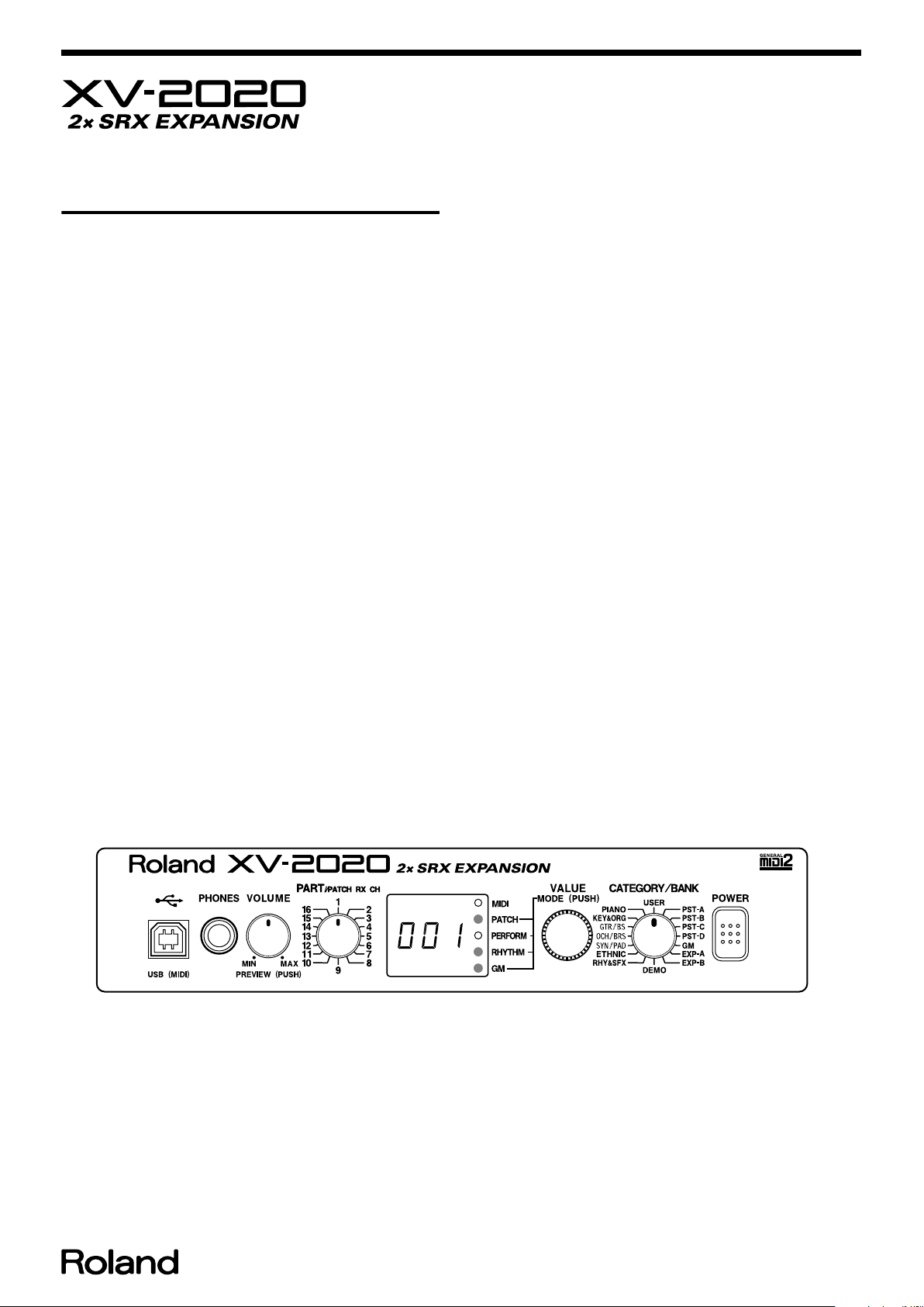
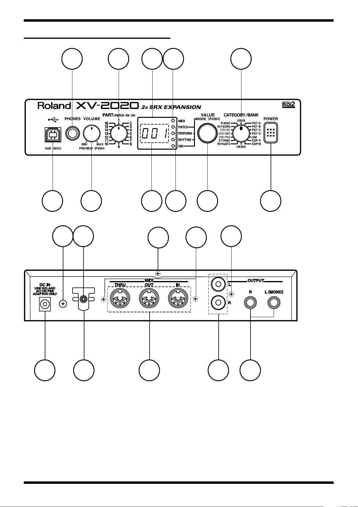
LOCATION OF CONTROLS
fig.haichi-front
fig.rear-haichi
1
11
2
10 7
9
8
3 4
5 6
a b d
c
d
12 13 14 15
16
2
Page 4

LOCATION OF CONTROLS PARTS LIST
[Parts]
No PART CODE Part name Description Q’TY
1 02781189 YKF45-0021 USB CONNECTOR 1
2 01899212 P R-KNOB MF-A BLK/LCG 1
01789523 RK0971214 (W/N&W) 9M/M ROTARY POT. 1
3 00451423 LB-303VA 7SEG LED 1
4 00348490 SLR-325VCT31 LED (RED) 4
5 01785790 RK09710EL-5R4611 (W/N&W) ROTARY ENCODER 1
22485307 M R-KNOB L BLK 248-307 1
6 32490595 P S-KEY MX BLK 1
01676512 SDKLA1-B PUSH SWITCH 1
7 01785212 SRRS1G-F0615-1 (W/N&W) SWITCH (DIGITAL SW) 1
01899212 P R-KNOB MF-A BLK/LCG 1
8 00560745 SLR-325MCT31 LED (GREEN) 1
9 01785423 DISPLAY COVER 1
10 01785212 SRRS1G-F0615-1 (W/N&W) SWITCH (DIGITAL SW) 1
01899212 P R-KNOB MF-A BLK/LCG 1
11 13449172 HLJ7000-01-3010 6.5MM JACK 1
12 13449720 HEC2305-01-250 DC JACK 1
13 22360712 CORD HOOK 236-712 1
14 13429273 YKF51-5046 (TRIPRET) MIDI CONNECTOR 1
15 00677423 YKC 21-3035 RAC SOCKET 1
16 13449283 HLJ7101-01-3010 6.5MM JACK 2
XV-2020
[Screws]
No PART CODE Part name Description Q’TY
a 40011378 SCREW M4X8 BINDING TAPTITE S FE BZC 1
b 40011101 SCREW 3X8 BINDING TAPTITE B BZC 1
c 40011090 SCREW 3X6 BINDING TAPTITE B BZC 1
d 40011312 SCREW 3X8 BINDING TAPTITE P BZC 3
3
Page 5
Jul.2002
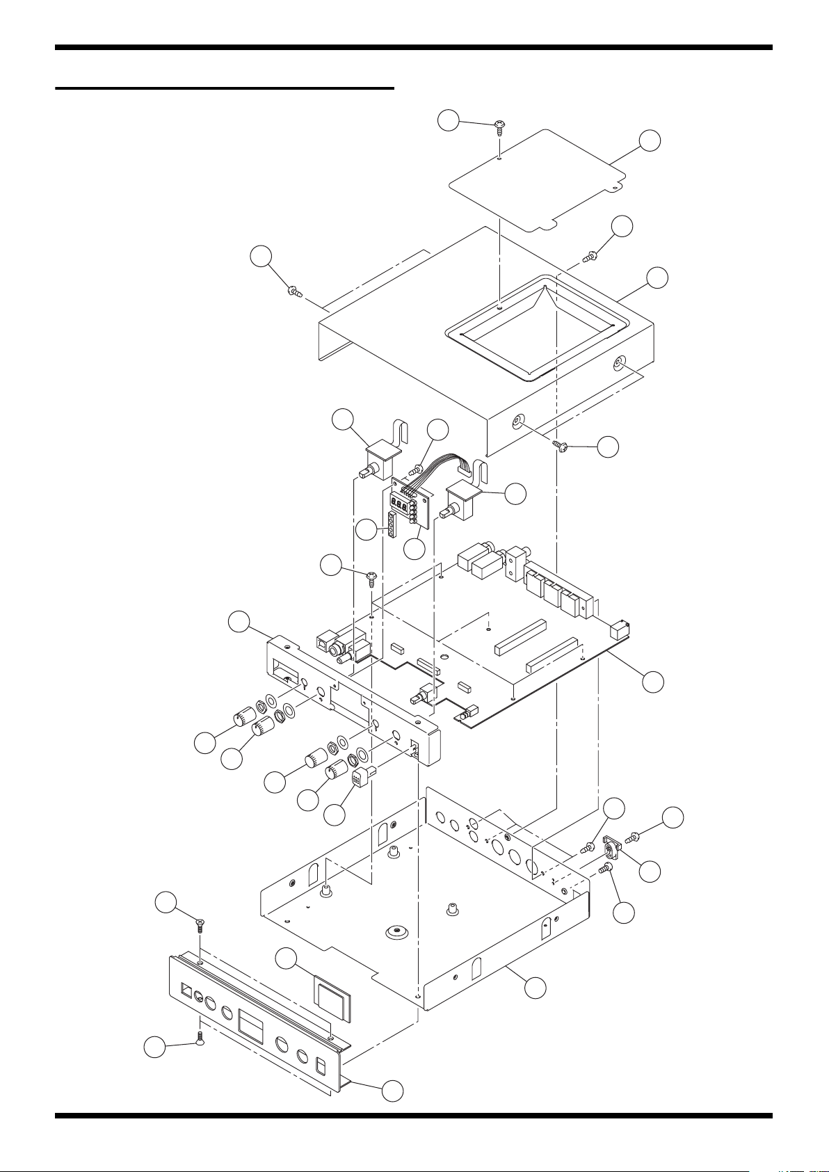
EXPLODED VIEW
fig.explo
e
13
e
e
12
6
8
d
4
1
1
2
1
3
d
e
6
7
5
c
b
4
14
f
10
11
f
9
a
Page 6

EXPLODED VIEW PARTS LIST
[Parts]
PART CODE Part name Description Q’TY
No
1 01899212 P R-KNOB MF-A BLK/LCG 3
2 22485307 M R-KNOB L BLK 248-307 1
3 32490595 P S-KEY MX BLK 1
4 03011489 FRONT HOLDER 1
5 72126401 MAIN BOARD ASSY 1
6 72126423 D-SW BOARD ASSY 2
7 72126412 LED BOARD ASSY 1
8 01785467 ISOLATOR LED MASK 1
9 03011490 FRONT PANEL 1
10 01785423 DISPLAY COVER 1
11 03011478 BOTTOM CHASSIS 1
12 03011845 TOP COVER 1
13 03011467 EXP COVER SRX2 1
14 22360712 CORD HOOK 236-712 1
[Screws]
No PART CODE Part name Description Q’TY
a 40011378 SCREW M4X8 BINDING TAPTITE S FE BZC 1
b 40011101 SCREW 3X8 BINDING TAPTITE B BZC 1
c 40011312 SCREW 3X8 BINDING TAPTITE P BZC 3
d 40011056 SCREW 3X6 BINDING TAPTITE B ZC 7
e 40011090 SCREW 3X6 BINDING TAPTITE B BZC 6
f 40011145 SCREW 3X6 FLAT TAPTITE B BZC 4
XV-2020
5
Page 7
Jul.2002
PARTS LIST
fig.part1e
SAFETY PRECAUTIONS:
The parts marked have
safety-related characteristics. Use
only listed parts for replacement.
NOTE: The parts marked # are new. (initial parts)
CASING
# 03011490 FRONT PANEL 1
# 03011467 EXP COVER SRX2 1
# 03011845 TOP COVER 1
CHASSIS
#
# 03011489 FRONT HOLDER 1
KNOB, BUTTON
SWITCH
01785423
03011478 BOTTOM CHASSIS 1
32490595
01899212 P R-KNOB MF-A BLK/LCG 3
22485307 M R-KNOB L BLK 248-307 1
01676512
01785212 SRRS1G-F0615-1 (W/N&W) SWITCH (DIGITAL SW) SW3,SW2 on DSB 1
CONSIDERATION ON PARTS ORDRING
When ordering any parts listed in the parts list, please specify the following items in the order sheet.
Failure to completely fill the above items with correct number and description will result in delayed or even
undelivered replacement.
DISPLAY COVER 1
P S-KEY MX BLK 1
SDKLA1-B PUSH SWITCH SW4 on MAB 1
QTY PART NUMBER DESCRIPTION MODEL NUMBER
Ex. 10 22575241 Sharp Key C-20/50
15 2247017300 Knob (orange) DAC-15D
JACK, EXT TERMINAL
DISPLAY UNIT
PCB ASSY
#
# 72126412 LED BOARD ASSY 1
# 72126423 D-SW BOARD ASSY 2
# 03014701 RIBBON CABLE JWFV 5 X 50 - P2.0 1
IC
# 03011045 HD6437016E SYTK3 IC (32BIT CPU) IC5 on MAB 1
# 03011201 UPD23C128040ALGY-527-MJH IC (MASK ROM) IC40 on MAB 1
# 03011212 UPD23C128040ALGY-528-MJH IC (MASK ROM) IC41 on MAB 1
13429273
00677423 YKC 21-3035 RAC SOCKET JK7 on MAB 1
02781189 YKF45-0021 USB CONNECTOR JK2 on MAB 1
13449172 HLJ7000-01-3010 6.5MM JACK JK4 on MAB 1
13449283 HLJ7101-01-3010 6.5MM JACK JK5,JK6 on MAB 2
13449720 HEC2305-01-250 DC JACK JK3 on MAB 1
00451423
NOTE: Replacement LB-303VA should be made on a unit base.
72126401 MAIN BOARD ASSY 1
NOTE: ‘MAIN BOARD ASSY’ includes the following parts.
01902756 PWB SPACER RSPS-12L 2
02019034 PWB SPACER RSPLS-12L 2
NOTE: ‘LED BOARD ASSY’ includes the following parts.
01456101 WIRING 12X120-P2.0-51065-51015-F CN2 on LEB 1
NOTE: ‘D-SW BOARD ASSY’ includes the following parts.
02902867
02677490 RA0C-003XP7TC203C180AF003 IC (CUSTOM) IC24 on MAB 1
02450401 GM71C18163CJ-6 IC (DRAM) IC8 on MAB 1
02453389 LC32V4265T-25 IC (DRAM) IC30 on MAB 1
01906689 BR24C08F-E2 IC (EEPROM) IC17 on MAB 1
02454867 TC58FVB321FT-10 IC (FLASH MEMORY) IC2 on MAB 1
YKF51-5046 (TRIPRET) MIDI CONNECTOR JK1 on MAB 1
LB-303VA 7SEG LED LED1 on LEB 1
M37641M8-137FP VER1.00 IC (8BIT CPU) IC19 on MAB 1
6
Page 8

XV-2020
IC
TRANSISTOR
01451578
15269219H0 HD74LS05FPEL IC (TTL) IC10 on MAB 1
01458401 TC74LVX4245FS(EL) IC (TTL) IC13,IC11 on MAB 2
01679412 TC7W139F(TE12L) IC (CMOS) IC21 on MAB 1
15249111 TC7WU04F(TE12L) IC (CMOS) IC26 on MAB 1
15249121 TC7W04F(TE12L) IC (CMOS) IC20 on MAB 1
01348945 TC7SH32FU(TE85L) IC (CMOS) IC18 on MAB 1
02451690 HD74LV08ATELL IC (CMOS) IC42 on MAB 1
02451712 HD74LV14ATELL IC (CMOS) IC22 on MAB 1
02675656 HD74LV11ATELL IC (CMOS) IC3 on MAB 1
02675689 HD74LV245ATELL IC (CMOS) IC6,IC4,IC1,IC9 on MAB 4
15189261 M5218AFP-600E IC (BIPOLAR OP AMP) IC36,IC32 on MAB 2
15289105 UPC4570G2-E2 IC (BIPOLAR OP AMP) IC37 on MAB 1
00344390 TA7805F(TE16L) IC (REGULATOR) IC33 on MAB 1
01678512 UPC2933T-T2 IC REGULATOR IC14 on MAB 1
02235378 TA78M05F(TE16L) IC (REGULATOR) IC35 on MAB 1
00458312 NJM2360M IC (REGULATOR) IC34 on MAB 1
15199937 M51953BFP-600C IC (RESET) IC15 on MAB 1
02900545 PC410LKNIP IC (PHOTO COUPLER) IC7 on MAB 1
00901523
02671023 2SC3052-T12-1E TRANSISTOR Q29 on MAB 1
15319116 2SC4154-T11-F TRANSISTOR Q27 on MAB 1
02905501 SSM3J02T TRANSISTOR Q30 on MAB 1
01783612 RN2426(TE85L) TRANSISTOR Q10,Q13,Q11,Q12 on MAB 4
02671256 RT1P141C-T12-1 TRANSISTOR Q18,Q17,Q16,Q15,Q14,Q19,Q21,Q20,Q1 on
02780056 RT1N144M TRANSISTOR Q28 on MAB 1
15329516 DTC114EKT146 TRANSISTOR Q3,Q6,Q7,Q8,Q4,Q5,Q9,Q2 on MAB 8
15329536 RN1442-A(TE85L) TRANSISTOR Q25,Q23,Q31,Q32,Q22,Q24 on MAB 6
AK4324-VF-E2 IC (DAC) IC38 on MAB 1
2SA1681 (SC-62)(POW SW) TRANSISTOR Q26 on MAB 1
MAB
9
DIODE
RESISTOR
01017512
15039142 S5688G(TPB5) 1A/400V RECTIFIER DIODE D1 on MAB 1
01897189 MA147-(TX) ARRAY DIODE DA7,DA2,DA1 on MAB 3
15339130 MA142WK-(TX) ARRAY DIODE DA3,DA4,DA5,DA6 on MAB 4
00348490 SLR-325VCT31 LED (RED) LED2,LED3,LED4,LED5 on LEB 4
00560745 SLR-325MCT31 LED (GREEN) LED6 on LEB 1
00566867
00566934 RPC05T 330 J MTL.FILM RESISTOR R58,R57 on MAB 2
00567034 RPC05T 121 J MTL.FILM RESISTOR R22 on MAB 1
00567045 RPC05T 151 J MTL.FILM RESISTOR R55,R53,R52,R51,R49,R56,R50,R54 on MAB 8
00567067 RPC05T 221 J MTL.FILM RESISTOR R19,R34,R18,R20,R17 on MAB 5
00567089 RPC05T 331 J MTL.FILM RESISTOR R155 on MAB 1
00567112 RPC05T 471 J MTL.FILM RESISTOR R76,R41 on MAB 2
00567123 RPC05T 561 J MTL.FILM RESISTOR R182,R127,R180,R119,R184,R115,R131,R178
00567156 RPC05T 102 J MTL.FILM RESISTOR R59,R70,R71,R146,R69 on MAB 5
00567167 RPC05T 122 J MTL.FILM RESISTOR R114,R118,R126,R130,R179,R183,R177,R181
00567178 RPC05T 152 J MTL.FILM RESISTOR R60 on MAB 1
00567190 RPC05T 222 J MTL.FILM RESISTOR R95 on MAB 1
00567289 RPC05T 103 J MTL.FILM RESISTOR R38,R43,R25,R27,R28,R157,R133,R137,R141,
00567301 RPC05T 153 J MTL.FILM RESISTOR R139 on MAB 1
00567378 RPC05T 473 J MTL.FILM RESISTOR R140 on MAB 1
00567390 RPC05T 683 J MTL.FILM RESISTOR R87,R93 on MAB 2
00567412 RPC05T 104 J MTL.FILM RESISTOR R152,R135,R156,R185 on MAB 4
00567556 RPC05T 105 J MTL.FILM RESISTOR R158,R72,R159,R162 on MAB 4
01011256 SR73K2ETD 0.47JOHM 1/2W MTL.FILM RESISTOR R160 on MAB 1
15399952 MCR50JZH470 1/2W CHIP RESISTOR R98,R102,R107,R97 on MAB 4
00566912 RPC05T 220 J MTL.FILM RESISTOR R2,R1,R5,R4,R3,R8,R10,R12,R14,R15,R23,R2
00567023 RPC05T 101 J MTL.FILM RESISTOR R21,R138,R136,R82,R79,R81,R80 on MAB 7
00567245 RPC05T 472 J MTL.FILM RESISTOR R113,R26,R117,R120,R123,R125,R129,R132,
01011856 RPC05T 0R0 J MTL.FILM RESIST0R R9,R11,R174,R173,R16,R166,R165,R163,R15
00567212 RPC05T 332 J MTL.FILM RESISTOR R37,R112,R116,R124,R128 on MAB 5
00567267 RPC05T 682 J MTL.FILM RESISTOR R99,R92,R88,R86,R94 on MAB 5
00567278 RPC05T 822 J MTL.FILM RESISTOR R100,R105 on MAB 2
00567323 RPC05T 223 J MTL.FILM RESISTOR R13,R101,R106 on MAB 3
RB411D T146 SCHOTTKY DIODE D2 on MAB 1
RPC05T 100 J MTL.FILM RESISTOR R110 on MAB 1
on MAB
on MAB
R144,R145,R121,R150,R172,R167,R168,R169
,R170,R171,R176,R29,R149,R47,R78,R75,R74
,R68,R67,R66,R64,R63,R62,R83,R48,R46,R10
8,R103,R61 on MAB
4,R7,R6 on MAB
R111 on MAB
3,R32,R30,R151,R148,R143,R142,R77,R73,R6
5,R45,R33,R161 on MAB
8
8
38
14
9
21
7
Page 9

Jul.2002
RESISTOR
01457145
01906656 MNR14 EOAB J 000 RESISTOR-ARRAY RA29,RA31 on MAB 2
01906678 MNR14 EOAB J 103 RESISTOR-ARRY RA54,RA51,RA37,RA36,RA40,RA52,RA38,
02125501 MNR14 EOAB J 220 RESISTOR-ARRAY RA7,RA6,RA5,RA2,RA1,RA8,RA4,RA24,R
# 02675712 MNR14 EOAB J 472 RESISTOR-ARRAY RA28,RA30 on MAB 2
POTENTIOMETER
01789523
CAPACITOR
01674189
01674190 ECUV1H150JCV CERAMIC CAPACITOR C80,C81 on MAB 2
01674212 ECUV1H220JCV CERAMIC CAPACITOR C23,C24 on MAB 2
01674301 ECJ1VC1H680J CERAMIC CAPACITOR C91,C99 on MAB 2
01674390 ECUV1H271JCV CERAMIC CAPACITOR C101 on MAB 1
01674423 ECUV1H471JCV CERAMIC CAPACITOR C22 on MAB 1
01674445 ECUV1H681JCV CERAMIC CAPACITOR C46 on MAB 1
01674612 ECJ1VB1H103K CERAMIC CAPACITOR C62,C165,C63 on MAB 3
01674712 ECJ1VF1A105Z CERAMIC CAPACITOR C35,C17,C86,C87,C88,C16,C18 on MAB 7
02129534 ECJ1VB1H102K CERAMIC CAPACITOR C168 on MAB 1
02456778 ECJ1VB1C104K CERAMIC CAPACITOR C44 on MAB 1
01674701 ECJ1VF1E104Z 0.1UF/16VK CERAMIC CAPACITOR C158,C31,C157,C75,C32,C36,C136,C155,C1
01674167 ECUV1H100DCV CERAMIC CAPACITOR C107,C117 on MAB 2
01674334 ECUV1H101JCV CERAMIC CAPACITOR C137,C195,C130,C109,C108,C82,C49,C29,C
02236712 AMZV0050J221 0200 POLYEST. CAPACITOR C128,C132,C138,C124 on MAB 4
00236223 AMZV0050J681 0200 POLYEST. CAPACITOR C125,C133 on MAB 2
01900823 RA2-16V100M-T2 CHEMICAL CAPACITOR C123,C112,C121,C142,C144,C146,C148,C11
01900834 RA2-16V101M-T2 CHEMICAL CAPACITOR C104,C127,C97,C179,C178,C90,C134,C98 on
01902590 RA2-6V101MC-T2 CHEMICAL CAPACITOR C100 on MAB 1
01902867 RA2-25V101M-T2 CHEMICAL CAPACITOR C141 on MAB 1
02239623 RA2-16V102M-T2 CHEMICAL CAPACITOR C94 on MAB 1
02891678 RE3-6V331M-T2 CHEMICAL CAPACITOR C106 on MAB 1
02891767 RC2-16V100M-T2 CHEMICAL CAPACITOR C180,C13,C41,C65,C152,C153,C154,C170,C
02894390 RA2-25V330MC-T2 CHEMICAL CAPACITOR C151 on MAB 1
02897889 RC2-16V470M-T2 CHEMICAL CAPACITOR C30,C33 on MAB 2
02898101 RA2-50V2R2MC-T2 CHEMICAL CAPACITOR C48 on MAB 1
13629624S0 6SC10M+T (OS) 6.3V10 CHEMICAL CAPACITOR C105 on MAB 1
EXBE10C103J RESISTOR ARRAY RA11,RA14,RA44,RA47 on MAB 4
RA50,RA42,RA17,RA53 on MAB
A49,RA48,RA46,RA45,RA27,RA25,RA9,RA
23,RA22,RA20,RA19,RA18,RA15,RA13,RA
10,RA26 on MAB
RK0971214 (W/N&W) 9M/M ROTARY POT. VR1 on MAB 1
ECUV1H120JCV CERAMIC CAPACITOR C50,C51 on MAB 2
60,C163,C147,C156,C25,C139,C14,C15,C19,
C149,C21,C145,C164,C169,C167,C162,C140,
C26,C143,C20,C194,C202,C159,C200,C199,
C198,C161,C196,C74,
C177,C176,C175,C174,C173,C172,C171,C19
7,C52,C37,C38,C39,C40,C42,C201,C47,C73,
C57,C64,C66,C67,C69,C70,C72,C43,C8,C102
,C103,C6,C7,C93,C95,C131,C5,C1,C4,C3,C7
6,C77,C89,C110,C96,C9,C113,C10,C116,C12
0,C92,C12 on MAB
11,C193 on MAB
5 on MAB
MAB
2,C166 on MAB
11
24
86
10
8
8
10
INDUCTOR, COIL, FILTER
00237212
01346089 SBC3-331-551 CHOKE COIL L16,L14 on MAB 2
01340834 EXCML20A390 FERRITE-BEAD L12 on MAB 1
01565578 N1608Z601T01 FERRITE-BEAD L24,L25,L26,L27,L6,L28,L23,L30,L18,L33,L3
01909645 EXCML16A270U FERRITE-BEAD L7,L8 on MAB 2
CRYSTAL, RESONATOR
00891801
00901912 MA-406 24.576MHZ TE24 CRYSTAL X3 on MAB 1
01126267 MA-406 7.056MHZ CRYSTAL X1 on MAB 1
ENCODER
01785790
CONNECTOR
02010078 TX25-80P-6ST-E1 CONNECTOR CN10,CN11 on MAB 2
13369600 52147-0510(5P) WIRE TRAP CN5,CN7 on MAB 2
8
SH-202 CHOKE COIL FL1 on MAB 1
27
4,L29,L22,L21,L19,L17,L15,L13,L11,L10,L9,
L5,L3,L2,L1,L20,L4 on MAB
MA-406 24.000MHZ TE24 CRYSTAL X2 on MAB 1
RK09710EL-5R4611 (W/N&W) ROTARY ENCODER EN1 on MAB 1
Page 10

XV-2020
CONNECTOR
SCREW
PACKING
#
# 03011578 PAD SIDE 1
# 03011590 PAD CARTON LOWER 1
# 03011545 PACKING CASE 1
# 03011623 OUTER PACKING CASE 1
MISCELLANEOUS
ACCESSORIES (STANDARD)
# 03011534 CD-ROM V1.00 1
# 72125967 OWNER’S MANUAL JAPANESE 1
# 72125990 OWNER’S MANUAL ENGLISH 1
13369934
13429294 51048-0500(5P) CABLE HOLDER CN4,CN6 on DSB 1
40011056
40011090 SCREW 3X6 BINDING TAPTITE B BZC 6
40011145 SCREW 3X6 FLAT TAPTITE B BZC 4
40011312 SCREW 3X8 BINDING TAPTITE P BZC 3
40011378 SCREW M4X8 BINDING TAPTITE S FE BZC 1
40011101 SCREW 3X8 BINDING TAPTITE B BZC 1
03011556 PAD 1
22360712
01785467 ISOLATOR LED MASK 1
00905756
00905767 AC ADAPTOR ACI-120C 1
01018312 AC ADAPTOR ACI-230C 1
01901578
01903356 AC CORD SET 230V 1.0M FOR PSB 1
01903367 AC CORD SET 240V 1.0M FOR PSB 1
00905234
40232334 WARRANTY CARD MOCHIKOMI JAPAN ONLY 1
01676412 FOOT SET RUBBER FOOT * 4 PCS 1
53253-1210 (2MM PITCH) CONNECTOR CN3 on MAB 1
SCREW 3X6 BINDING TAPTITE B ZC 6
CORD HOOK 236-712 1
AC ADAPTOR ACI-100C 1
AC ADAPTOR WITHOUT AC CORD
ECP01-5A (PLUG FOR BRC-230T)
PSB-1U UNIVERSAL
EURO CONVERTER PLUG 1
1
9
Page 11

Jul.2002
CHECKING THE VERSION NUMBER
1.
While holding down [VOLUME], press [VALUE].
2.
Turn [CATEGORY/BANK] to choose “UTILITY (PIANO).”
3.
When you rotate [VALUE], the program version (number) is displayed.
4.
While holding down [VOLUME], press [VALUE].
The XV-2020 exits Edit mode.
SAVING AND LOADING DATA
Save performance, patch and rhythm set setting in the user area of the main
unit of XV-2020 and system setting to the PC as SVD file with the attached XV
editor.
Saving user data
1.
Connect the XV-2020 and the PC using a USB cable.
The PC to be connected shall be installed with XV-2020 driver and XV editor.
2.
Turn on the main power of XV-2020 and start up the XV Editor.
3.
Select [File]->[Save SVD file] in the menu.
4.
Specify the saving place and file name and then select [OK].
fig.Sur
5.
Press [VALUE] once more to execute the factory reset.
To cancel the procedure, while holding down [VOLUME] and pressing
[VALUE].
If there is important data you’ve created that’s stored in memory, all such data
is discarded, and everything is returned to the factory defaults when a Factory
Reset is performed. If important data is stored in the unit, save it on an
external device.
You cannot carry out this procedure when “DEMO” is selected with the
[CATEGORY/BANK] knob.
SYSTEM SOFTWARE UPDATE PROCEDURE
The XV-2020 uses a Flash Memory for the program ROM.
The version may be updated by externally sending the MIDI data.
Whenever updating is performed, factory setting must be restored.
If the user memory is written with important data, save data before updating.
Loading user data
1.
Connect the XV-2020 and the PC using a USB cable.
The PC to be connected shall be installed with XV-2020 driver and XV editor.
2.
Turn on the main power of XV-2020 and start up the XV Editor.
3.
Select [File] -> [Load SVD file] in the menu.
4.
Specify the saving place and file name and then select [OK].
RESTORING THE FACTORY SETTINGS
When using the XV-2020 for the first time, start by returning the settings to
their factory defaults so that the XV-2020 operates as described in the
procedures in the owner’s manual.
This returns all settings stored in memory in the XV-2020 to the values they
had when the unit was shipped from the factory.
1.
While holding down [VOLUME], press [VALUE].
The indication in the display begins flashing, and the mode changes.
2.
Turn [CATEGORY/BANK] to choose PIANO (UTILITY).
3.
Rotate [VALUE] until “Fct” appears in the display.
fig.Fct
What is needed
• XV-2020 Update Disk (2HD:3 disks) (No.17041190)
• A sequencer that can play an SMF (a synthesizer with a sequencer such
as the FANTOM may be used)
• MIDI cable
Updating
1.
Connect MIDI OUT of the external sequencer to MIDI IN of the XV-2020
with the MIDI cable.
Set the sequencer to enable chain play of SMF.
2.
Turn on the power while pressing [VOLUME] and [VALUE] and
continue pressing until [mid] is displayed.
fig.mid
3.
Releasing will display [---] and enters data receive waiting status.
fig.---
4.
Press [VALUE]; “Sur” flashes in the display, and a confirmation screen
appears.
10
4.
After confirming the display shown in step 3., play all “.mid” files on the
XV-2020 UPDATE DISKS 1 to 3 from the external sequencer. “r...” is
displayed during MIDI data receiving.
Page 12

XV-2020
fig.rcv
5.
When updating is completed without an error, [Fin] is displayed, and 4
LEDs, [PATCH], [PERFORM], [RYTHM] and [GM] blink simultaneously.
fig.Fin
6.
Restart the power and confirm that the system has been properly
updated.
7.
Finally, restore factory setting. This completes the update.
* When you fail in update, start the updating from the beginning.
TEST MODE
What is needed
• Headphone
• Monitor speakers (MA-12, etc.) 2pcs
• Audio cables 2pcs
• Audio cables (RCA type) 2pcs
• MIDI cable 1pcs
• USB cable 1pcs
• Wave expansion board SRX series 2pcs
• PC on which operation of XV-2020 is confirmed.
Precautions for the test
• The user data may be deleted when entering the test mode .
Always back up your data. (Saving and loading user data reference)
• Some test items produce verification sound.
• Mount the wave expansion board prior to turning the unit’s power on.
Connect the headphone and the monitor speaker in advance.
3.
Release and then promptly press [VOLUME] again while the [PATCH]
LED is turned on.
4.
“tSt” will be displayed and automatically proceed to LED Test.
fig.tSt
Exiting the Test mode
Turn off the power. Turning on the power again returns to normal mode.
Do not turn off the power during restoration of factory setting.
Proceeding to the next test item
If no error occurs during the Memory, Expansion Board, USB and MIDI tests,
the system automatically proceeds to the next test item.
For Program Version, Encoder and Rotary Switch Tests, pressing [VALUE]
proceeds to the next test item.
For Sound Test, pressing [VOLUME] proceeds to the next test item.
Proceeding through test items
At LED Test, setting [CATEGORY] to PIANO enters individual test mode and
enables to proceed to each test item by rotating [CATEGORY].
[PIANO] 2 :Program Version
[USER] 3 :Memory Test
[PST-A] 4 :Expansion Board Test
[PST-B] 5 :USB Test
[PST-C] 6 :MIDI Test
[PST-D] 7 :Sound Test
[GM] 8 :Encoder Test
[EXP-A] 9 :Rotary Switch Test
[EXP-B] 10 :Factory Reset
In individual test mode, the system does not automatically proceed to the
other items after completion of one test.
Test items
The XV-2020 provides the following tests:
For information on each test, refer to each item.
1.
LED Test
2.
Program Version
3.
Memory Test
4.
Expansion Board Test
5.
USB Test
6.
MIDI Test
7.
Sound Test
8.
Encoder Test
9.
Rotary Switch Test
10.
Factory Reset
Operating buttons
Entering the Test mode
1.
Set [PART] to 15 and [CATEGORY] to KEY&ORGAN.
2.
Turn on the power while pressing [VOLUME].
Details of test items
1 :LED Test
fig.LEDtSt
The LEDs lights up on the display in the following order: [MIDI], [PATCH],
[PERFORM], [RHYTHM], [GM].
Simultaneously, the letter “8.” comes on from the left.
If the LED does not come on or go off, check the following parts.
PANEL BOARD LED1-6, CN2
MAIN BOARD CN3, L19-30, R49-56, R1-8, RA1, Q2-Q13
2 : Program Version
fig.vEr
• Check the version number of the CPU (Internal ROM) and the ROM
11
Page 13

Jul.2002
(External ROM).
The version of the CPU (Internal ROM) is displayed as follows:
[PATCH] LED comes on if CPU version is 1.00
[PERFORM] LED comes on if CPU version is 1.01
[RHYTHM] LED comes on if CPU version is 1.02
[GM] LED comes on if CPU version is 1.03
The version of ROM (External ROM) is displayed on 7 SEG LED.
fig.101
Update if the version number is inappropriate.
See “PROCEDURE FOR UPDATING” for the updating procedure.
3:Memory Test
fig.mEm
• [Goo] is displayed if no errors occur during the memory test, and
automatically proceed to the next test.
fig.Goo
Display
Wave ROM Error
check part:MAIN BOARD IC40, 41
4 :Expansion Board Test
fig.ExP
Slot A and B of wave expansion board will be tested.
• [Goo] is displayed if no errors occur, and automatically proceed to the
next test.
fig.Goo
If any error occurs, it will be displayed as follows: Check the parts
corresponding to the error displayed.
Display
Exp Board A Error
check part:MAIN BOARD IC24,
CN10
If any error occurs, it will be displayed as follows: Check the parts
corresponding to the error displayed.
Display
Internal ROM Error
check part:MAIN BOARD IC5, X1,
R41
External ROM Error
check part:MAIN BOARD IC2
DRAM Error
check part:MAIN BOARD IC8
EEPROM Error check part
:MAIN BAORD IC17
DSP Internal RAM Error
check part:MAIN BOARD IC24, 26,
X3
Exp Board B Error
check part:MAIN BOARD IC24,
CN11
5 :USB Test
fig.USb
Turn on the PC’s power prior to this test.
• Connect the PC and the XV-2020 using a USB cable. Confirm that the
[MIDI] LED comes on.
[Goo] is displayed if disconnection after pulling out the USB cable can be
recognized correctly, and automatically proceeds to the next test.
fig.Goo
12
DSP External RAM Error
check part:MAIN BOARD IC30
• If [Goo] is not displayed properly, check the following parts
MAIN BOARD IC19, R155, X2, JK2
6 :MIDI Test
fig.mid
Page 14

XV-2020
Connect MIDI IN and MIDI OUT with the MIDI cable in loop and confirm that
the [MIDI] LED lights up.
[Goo] is displayed if disconnection after pulling out the cable of either MIDI
IN or MIDI OUT can be recognized correctly, and automatically proceeds to
the next test.
fig.Goo
• If [Goo] is not displayed properly, check the following parts
MAIN BOARD IC7, 10
7 :Sound Test
On entering this test, at first, sound is produced from OUTPUT L (MONO),
OUTPUT L (RCA Type) and left side of the headphone.
Output is switched by each pressing of [VALUE].
Display sound status
Lch sine wave
Sound is produced from OUTPUT
L(MONO), OUTPUT L (RCA Type)
and left side of headphone.
Rch square wave
Sound is produced from OUTPUT
R, OUTPUT R (RCA Type) and
right side of headphone.
Center sine wave
Sound is produced from all outputs.
fig.Enc30to0
After confirming the second piano tone, pressing [VALUE] proceeds to the
next item.
• If the encoder does not count up or down properly, check the following
parts:
MAIN BOARD EN1 and IC22.
9 :Rotary Switch Test
fig.rot
Confirm that rotating [PART] to the right changes the display as follows:
After one revolution, a bell rings.
Display [PART]
15
After confirming 3 types of output, pressing [VOLUME] proceeds to the next
item.
• If the sound is not output properly, check the following parts:
MAIN BOARD IC32,36,37,38,Q22-25,31,32,VR1,JK4,5,6,7
8 :Encoder Test
fig.Enc
Rotating the encoder to the right to count up the 7 SEG display from [1] to [30]
will play a piano tone.
fig.Enc1to30
16
1
2
:
:
16
1 (bell rings)
After confirming the piano tone, rotating the encoder to the left to count down
from [30] to [0] will play the piano tone again.
• If the display is not properly changed, check the following parts:
MAIN BAORD CN5 and Q14-17
D-SW BOARD CN4 and SW2
Confirm that rotating [CATEGORY] to the right changes the display as
follows:
After one revolution, a bell rings.
13
Page 15

Jul.2002
Display
:
CATERGORY
KEY&ORG
PIANO
USER
PST-A
:
PIANO
USER (bell rings)
• If the display is not properly changed, check the following parts:
MAIN BAORD CN7 and Q18-21
D-SW BOARD CN6 and SW3
After confirming the second bell, pressing [VALUE] proceeds to the next item.
10 :Factory Reset
fig.Fct
Pressing [VALUE] executes the restoration of factory setting.
When restoration of the factory reset is completed properly, a message, “cnP”
will be displayed.
fig.cnP
14
Page 16

XV-2020
15
Page 17

Jul.2002
BLOCK DIAGRAM
fig.sp2a3
XV-2020
D-SW
BOARD
PART
1
15
14
13
12
11
10
CN6
CN5
EN1
MODE(PUSH)
216
3
4
5
6
7
8
9
ENCODER
VALUE
LED BOARD
LED1
IC5
7SEG
CN2
CN3
LED
SW
LED6 (MIDI)
LED2 (PATCH)
LED3 (PERFORM)
LED4 (RHYTHM)
LED5 (GM)
MAIN BOARD
VSW
D-SW
BOARD
SW2SW3
CATEGORY/BANK
I
ANO
P
KEY&ORG
GTR/BSS
OCH/BRS PSTSYN/PAD
ETHNIC
RHY&SFX
USER
DEMO
CN4
CN7
PST-A
PST-B
PST-
GM
EXP-A
EXP-B
IC19
D+5V
JK3
DC IN
C
D
SW4
POWER SW
+9V
IC36
AMP
IC33
REGULATOR
IC35 IC34
REGULATOR
A+5V
JK4
IC14
REGULATOR
DC/DC
CONVERTER
PHONES
D+3.3V
A-5V
USB(MIDI)
JK2
VR1 IC32
1
VOL
USB
IC37
AMP
LPF
JK5
OUTPUT L (MONO)
OUTPUT R
JK6
JK7
ENCSW
ENCA
ENCB
X1
7.056MHz 24MHz
JK1
OUTTHRU IN
MIDI
CPU
HD647016F
(28.224MHz)
(x4)
RXD1
TXD1
D0-15
5V
5V 5V
ESDA
ESDL
IC17 IC8 IC2
Buffer
16bit 16bit
EEPROM
8Kbit
(1Kbit x 8bit)
5V
DRAM
16Mbit
(1Mbit x 16bit)
IC11, IC13
3.3V
(2Mbit x 16bit)
8bit
X2
Flash
32Mbit
3.3V3.3V
CPU(UIPC)
M37641M8
(12MHz)
(/2 )
16bit
IC24
TC203C180AF003
CK
X3
24.576MHz
IC38
DAC
AK4324
SDO
TONE
GENERATOR
(24.576MHz)
3.3V
ED0-78bit
IC30
DRAM
4Mbit
(256Kbit x 16bit)
3.3V
5V
16bit
OUTPUT L R
(RCA PIN)
CN10 SRX CONNECTOR
WD0-15
CN11 SRX CONNECTOR
IC40
IC41
ROM
128Mbit
(8Mbit x 16bit)
3.3V
1716
Page 18

Jul.2002
CIRCUIT BOARD
fig.pcb-main
18
View from components side
Page 19

XV-2020
View from foil side
19
Page 20

Jul.2002
CIRCUIT DIAGRAM(MAIN 1)
XV-2020
fig.dsp+
DA1
MA147-(TX)
21
JK1
YKF51-5046
4545
2
3234353930
L1
600L2600L3600
R17
R18
220
220
+
5D
3
Q1
RT1P141C
3 2
1
CN1
8
7
6
5
4
3
2
1
NIU
C30
47/16
LEDD[0..7]
SC[0..3]
OUTTHRU IN
22
2224252920
L4
L5
600
600
R19
R20
220
3
IC10A
HD74LS05FP
IC10C
HD74LS05FP
+
5D
R40
NIU
CPUOUT
CPUIN
MD1
FWP
XCPURST
D
DA4
MA142WK-(TX)
1 2
C31
0.1
+
5D
21
DA2
MA147-(TX)
DD
12
56
IC10E
1110
HD74LS05FP
+
5D
3
1
R21
100
R39
NIU
220
+
5D
8
7
6
5
4
3
2
1
+
5D
45
1214151910
+
5D
R27
10K
+
5D
R29
10K
XRST
MIDIOUT
MIDIIN
IC14
UPC2933T
IN
2
LEDD7
LEDD6
LEDD5
LEDD4
LEDD3
LEDD2
LEDD1
LEDD0
SC3
SC2
SC1
SC0
40
50
60
70
D
L6
600
R22
120
3
1 2
DA3
MA142WK-(TX)
IC10B
34
HD74LS05FP
IC10D
98
HD74LS05FP
R165
0
11
13
SW1A
R166
0
21
23
SW1B
3
OUT
GND
D
4 5
3 6
2 7
1 8
D
ESDA
ESCL
12
NIU
22
NIU
C32
0.1
R47
10K
TXD1
RXD1
LED7
LED6
LED5
LED4
LED3
LED2
LED1
LED0
SCAN3
SCAN2
SCAN1
SCAN0
1
3
+
64
+
5D
C28
NIU
+
D3.3
5D
R48
10K
C33
47/16
R1
22
R2
22
R3
22
RA1
22
R4
22
D[0..15]
A[0..21]
XUCS
XWR
+
D3.3
1
2
13
9
10
11
XXPWAIT
RA51
10K
RA52
10K
RA53
10K
RA54
10K
1 8
2 7
3 6
4 5
1 8
2 7
3 6
4 5
R38
10K
XXPINT
XRD
IC3A
12
HD74LV11AT
IC3C
8
HD74LV11AT
+
5D
RA50
10K
R171
10K
R172
10K
RA17
10K
D
IC42B
6
XPD
HD74LV08AT
B3XFCS
B3XFLCS
R5
22
R6
22
R7
22
R8
22
R11
0
MD1
TXD1
RXD1
+
R13
22K
1
2
3
5
6
D
53
2 4
C37
0.1
IC17
A0
A1
A2
SDA
SCL
BR24C08F
+
5D
C27
NIU
IC12
NIU
D
5D
R26
4.7K
MIDIOUT
MIDIIN
VCC
WP
VSS
+
5D
147
IC10G
HD74LS05FP
D
VSW
8
7
4
13 12
R43
10K
D
+
5D
7
4
D
R28
10K
FRDBY
+
5D
C36
0.1
D
IC10F
R44
NIU
HD74LS05FP
+
5D
R46
10K
6
VCC
NC
RST
NC
NC
NC
DLY
GND
IC15
M51953BFP-600C
ESCL_SRX
ESDI_SRX
ESDO_SRX
+
5D
USBCABL
ENCSW
ENCB
ENCA
+
5D
D
D
1
2
3
8
5
C35
1
9
10
D D
C12
0.1
IC7
5
PC410
D
+
5D
R42
NIU
D
RSD1
RSD0
R34
220
C22
470P
C23
22P
C24
22P
R45
0
XRST
IC42C
8
HD74LV08AT
1 4
XRST
SCAN2
SCAN3
C15
0.1
X1
MA-406
7.056MHz
C4
0.1
C5
C6
0.1
0.1
C7
C8
0.1
0.1
+
5D
ESCL
ESDA
XFWP
XMUTE
LED7
LED6
LED5
ENCSW
ENCB
ENCA
R37
3.3K
R41
470
12
13
D
MD3
MD2
MD1
MD0
TXD1/PA4
RXD1/PA3
TXD0/PA1
RXD0/PA0
PE13
PE12
PE11
PE10
PE9
PE8
PE7/TIOC2B
PE6/TIOC2A
PE5/TIOC1B
PE4/TIOC1A
AN7/PF7
AN6/PF6
AN5/PF5
AN4/PF4
AN3/PF3
AN2/PF2
AN1/PF1
AN0/PF0
AVCC
AVSS
PLLVCC
PLLVSS
PLLCAP
EXTAL
XTAL
RES
VSS
3
23
VSS
21
VCC
VSS
VSS
27
33
+
147
+
5D
73
75
78
79
D
47
48
50
51
112
111
110
108
107
106
105
104
102
89
99
98
96
95
94
93
92
91
+
5D
100
97
D
80
C21
0.1
82
81
74
72
84
C29
100p
D
IC42D
11 C39
HD74LV08AT
+
5D
37
65
77
103
VCC
VCC
VCC
VCC
*/WAIT/IRQ6/A20
PB5/IRQ3/RDWR
PB4/IRQ2/CASH
PB3/IRQ1/CASL
VSS
VSS
VSS
VSS
39
55
61
71
90
5D
IC42E
HD74LV08AT
D
PB2/IRQ0/RAS
*/SCK1/IRQ1
*/SCK0/IRQ0
*/PE2/DREQ1
*/PE3/DRAK1
PE15/DACK1
*/PE0/DREQ0
*/PE1/DRAK0
VSS
101
R9
0
FWP
*/IRQ7/A21
PB7/A19
PB6/A18
PB1/A17
PB0/A16
PC15/A15
PC14/A14
PC13/A13
PC12/A12
PC11/A11
PC10/A10
PC9/A9
PC8/A8
PC7/A7
PC6/A6
PC5/A5
PC4/A4
PC3/A3
PC2/A2
PC1/A1
PC0/A0
PD15/D15
PD14/D14
PD13/D13
PD12/D12
PD11/D11
PD10/D10
PD9/D9
PD8/D8
PD7/D7
PD6/D6
PD5/D5
PD4/D4
PD3/D3
PD2/D2
PD1/D1
PD0/D0
PA13/WRH
PA12/WRL
PA14/RD
WDTOVF
*/PA7/CS3
*/PA6/CS2
PA11/CS1
PA10/CS0
*/PA9/IRQ3
*/PA8/IRQ2
NMI
*/AH/DACK0
CK/PA15
VSS
VSS
109
D
C167
0.1
+
5D
C2
10/16
D
IC5
32
31
30
29
22
20
19
1 8
2 7
18
3 6
17
4 5
16
15
1 8
2 7
14
13
3 6
12
4 5
1 8
11
10
2 7
9
3 6
4 5
8
7
1 8
2 7
6
5
3 6
4 5
4
52
4 5
3 6
53
2 7
54
56
1 8
4 5
57
3 6
58
2 7
59
1 8
60
62
4 5
63
3 6
64
2 7
1 8
66
4 5
67
3 6
68
2 7
69
70
1 8
36
SCAN0
38
34
28
35
24
26
25
44
45
40
41
42
43
46
49
76
87
88
2
85
86
1
83
HD64F7016F
XWR
XXPCS
0.1
XFUCS
XFLCS
XFLCS
R12
22
A21
R14
22
A19
A18
A17
A16
A15
A14 A14
A13
A12
A11
A10
A9
A8
A7
A6
A5
A4
A3
A2
A1
A0
D15
D14
D13
D12
D11
D10
D9
D8
D7
D6
D5
D4
D3
D2
D1
D0
R32
0
R33
0
1 8
2 7
3 6
4 5
SCAN1
D
LED3
LED4
LED1
LED2
LED0
D3.3
53
1
2
+
D3.3
IC3D
147
HD74LV11AT
D
RA18
22
XUOBF1
XUIBF0
EEPCS1
EEPCS0
+
C38
0.1
IC18
4
TC7SH32FU
D
R23
22
RA5
22
RA7
22
RA9
22
RA10
22
R15
22
R24
22
D4
D11
D5
D10
D6
D9
D7
D8
D0
D15
D1
D14
D2
D13
D3
D12
1 8
2 7
3 6
4 5
1 8
2 7
3 6
4 5
1 8
2 7
3 6
4 5
1 8
2 7
3 6
4 5
IC42A
3
HD74LV08AT
R164
NIU
XMUTE
XRST
+
XWR
XRD
RDWR
XCASH
XCASL
XRAS
XUCS
XFUCS
XFLCS
XXPCS
1
2
R141
10K
B3XXPWR
5D
R163
0
RA45
22
RA46
22
RA48
22
RA49
22
XCASL
RDWR
XCASH
XRAS
XUCS
XWR
XXPCS
XFLCS
XFUCS
XRD
XFWP
+
5D
4
5
D
XFLCS
XFUCS
XXPCS
XRD
XXPCS
XWR
XRD
XFWP
XRST
A21
A19
A18
A17
A16
A15
A13
A12
A11
A10
A9
A8
A7
A6
A5
A4
A3
A2
A1
A0
A10
A9
A8
A7
A6
A5
A4
A3
A2
A1
XRAS
XCASH
XCASL
RDWR
C1
+
D3.3
0.1
IC1
20
11
B8
12
B7
VCC
13
B6
14
B5
15
B4
16
B3
17
B2
18
B1
GND
10
D
+
D3.3
20
11
B8
12
B7
VCC
13
B6
14
B5
15
B4
16
B3
17
B2
18
B1
GND
10
D
C10
+
D3.3
0.1
IC6
20
HD74LV245AT
11
B8
12
B7
VCC
13
B6
14
B5
15
B4
16
B3
17
B2
18
B1
GND
10
D
C14
+
D3.3
0.1
IC9
20
HD74LV245AT
11
B8
12
B7
VCC
13
B6
14
B5
15
B4
16
B3
17
B2
18
B1
GND
10
D
IC8
A9
I/O15
A8
I/O14
A7
I/O13
A6
I/O12
A5
I/O11
A4
I/O10
A3
I/O9
A2
I/O8
I/O7
A1
I/O6
A0
I/O5
I/O4
I/O3
RAS
I/O2
UCAS
I/O1
LCAS
I/O0
WE
OE
VCC
NC
VCC
NC
NC
VCC
NC
NC
VSS
VSS
VSS
GM71C18163CJ-6
IC3B
HD74LV11AT
HD74LV245AT
IC4
HD74LV245AT
D
D
C3
0.1
D
D
D
D
28
27
26
25
24
23
20
19
18
17
14
30
31
13
29
11
12
15
D
16
32
+
5D
C13
10/16
D
3
4
6
5
DIR
DIR
DIR
DIR
RA2
22
9
1 8
2 7
3 6
4 5
R148
D
1 8
2 7
3 6
4 5
1 8
2 7
3 6
4 5
1 8
2 7
3 6
4 5
D
1 8
2 7
3 6
4 5
1 8
2 7
3 6
4 5
D
C17
1
RA4
22
R31
NIU
R10
22
D
+
0
RA6
22
RA8
22
RA13
22
RA15
22
5D
D
C18
1
B3XXPCS
B3XWR
B3XRD
B3XFWP
D15
D14
D13
D12
D11
D10
D9
D8
D7
D6
D5
D4
D3
D2
D1
D0
B3A21
B3A19
B3A18
B3A17
B3A16
B3A15
B3A14
B3A13
B3A12
B3A11
B3A10
B3A9
B3A8
B3A7
B3A6
B3A5
B3A4
B3A3
B3A2
B3A1
B3A0
R30
0
D8
D9
D10
D11
D12
D13
D14
D15
D0
D1
D2
D3
D4
D5
D6
D7
FRDBY
D
B3XRST
D3.3
R25
10K
RA19
22
4 5
3 6
2 7
1 8
4 5
3 6
2 7
1 8
RA22
22
RA24
22
4 5
3 6
2 7
1 8
4 5
3 6
2 7
1 8
RA26
22
+
A8
8
A7
7
A6
6
A5
5
A4
4
A3
3
A2
2
A1
19
OE
1
9
A8
8
A7
7
A6
6
A5
5
A4
4
A3
3
A2
2
A1
19
OE
1
9
A8
8
A7
7
A6
6
A5
5
A4
4
A3
3
A2
2
A1
19
OE
1
9
A8
8
A7
7
A6
6
A5
5
A4
4
A3
3
A2
2
A1
19
OE
1
41
40
39
38
36
35
34
33
10
9
8
7
5
4
3
2
1
6
21
22
37
42
C16
1
B3XFLCS
B3A21
B3A19
B3A18
B3A17
B3A16
B3A15
B3A14
B3A13
B3A12
B3A11
B3A10
B3A9
B3A8
B3A7
B3A6
B3A5
B3A4
B3A3
B3A2
B3A1
+
D3.3
B3XFCS
B3XWR
B3XRD
B3XFWP
R16
0
B3XWR
B3XRD
B3XFWP
B3XFLCS
B3XFCS
B3A1
B3A2
B3A16
B3A17
B3A0
B3A15
B3A14
B3A13
B3A12
B3A11
B3A10
B3A9
B3A21
B3A19
B3A18
B3A8
B3A7
B3A6
B3A5
B3A4
B3A3
D
10
9
8
7
6
5
4
3
22
2
C25
0.1
D
10
9
8
7
6
5
4
3
22
2
+
D3.3
C19
0.1
A8
A7
A6
A5
A4
A3
A2
A1
G
DIR
A8
A7
A6
A5
A4
A3
A2
A1
G
DIR
C180
10/16
D
IC2
13
NC
10
A20
9
A19
16
A18
17
A17
48
A16
1
A15
2
A14
3
A13
4
A12
5
A11
6
A10
7
A9
8
A8
18
A7
19
A6
20
A5
21
A4
22
A3
23
A2
24
A1
25
A0
26
CE
11
WE
28
OE
15
RY/BY
47
BYTE
14
WP/ACC
12
RESET
TC58FVB321FT-10
C11
100p
D
+
+
5D
D3.3
24
1
VCCA
VCCB23VCCB
GND11GND12GND
TC74LVX4245FS
13
D
+
+
5D
D3.3
24
1
VCCA
VCCB23VCCB
GND11GND12GND
TC74LVX4245FS
13
D
1 8
2 7
3 6
4 5
3
4
5
6
7
8
9 10
3
4
5
6
7
8
9 10
C20
0.1
IC11
14
B8
15
B7
16
B6
17
B5
18
B4
19
B3
20
B2
21
B1
C26
0.1
IC13
14
B8
15
B7
16
B6
17
B5
18
B4
19
B3
20
B2
21
B1
DQ15/A-1
+
D3.3
12
12
4 5
3 6
2 7
1 8
4 5
3 6
2 7
1 8
4 5
3 6
2 7
1 8
4 5
3 6
2 7
1 8
DQ14
DQ13
DQ12
DQ11
DQ10
DQ9
DQ8
DQ7
DQ6
DQ5
DQ4
DQ3
DQ2
DQ1
DQ0
VDD
VSS
VSS
RA20
22
RA23
22
RA25
22
RA27
22
RA42
10K
R149
10K
R167
10K
R169
10K
RA44
10K
RA47
10K
D
D
D
45
43
41
39
36
34
32
30
44
42
40
38
35
33
31
29
37
27
46
R150
10K
R168
10K
R170
10K
B3D15
B3D14
B3D13
B3D12
B3D11
B3D10
B3D9
B3D8
B3D7
B3D6
B3D5
B3D4
B3D3
B3D2
B3D1
B3D0
+
D3.3
D
B3D8
B3D9
B3D10
B3D11
B3D12
B3D13
B3D14
B3D15
B3D0
B3D1
B3D2
B3D3
B3D4
B3D5
B3D6
B3D7
C9
0.1
B3D4
B3D12
B3D5
B3D13
B3D6
B3D14
B3D7
B3D15
B3D11
B3D3
B3D10
B3D2
B3D9
B3D1
B3D8
B3D0
B3D[0..15]
B3A[0..21]
B3XRD
B3XWR
B3XXPCS
B3XRST
RA11
10K
3
4
5
6
7
8
9 10
3
4
5
6
7
8
9 10
RA14
10K
+
D3.3
12
12
2120
Page 21

Jul.2002
CIRCUIT DIAGRAM(MAIN 2)
XV-2020
kpab
XPULLUP
L727L8
JK2
YKF45-0021
27
R173
0
R60
1.5K
XUOBF1
XUIBF0
XUCS
A[0..21]
TC7W04F
123
R174
0
Q30
SSM3J02T
R185
100K
XRST
IC20C
62
4
10
20
D
L9
600
R151
0
D
R154
NIU
3 2
1
C52
0.1
D
EN1A
RK09710EL-5R4611
C45
NIU
R175
NIU
IC20B
TC7W04F
A21
A0
C192
NIU
D
R57
33
R58
RPC05T@J
33
C47
0.1
IC20A
TC7W04F
17
35
R65
0
+
5D
84
IC20D
TC7W04F
D
EN
AB
111213
D
C48
2.2/50
D
R63
10K
IC21A
TC7W139F
2
B
Y3
1
A
Y2
Y1
Y0
C49
100p
C57
0.1
EN1B
RK09710EL-5R4611
D
R162
1M
D
R152
100K
3
5
6
7
D
+
5D
C196
+
5D
0.1
R59
1K
D[0..15]
R66
10K
C46
680P
XWR
XRD
D
D
BUSPOWER
USBCABL
C51
12p
R67
10K
D
R68
10K
VBUS
SLEEP
R155
330
R69
1K
R70
1K
R71
1K
C62
0.01
D
R153
0
D7
D6
D5
D4
D3
D2
D1
D0
C63
0.01
C42
0.1
9
CNVSS/VPP
18
LPF
25
P87/RTS1
26
P86/CTS1
27
P85/URXD1
28
P84/UTXD1
29
P83/RTS2/STXD
30
P82/CTS2/SRXD
31
P81/URXD2SCLK
32
P80/UTXD2/SRDY
70
USB-D+
71
USB-D-
72
EXTCAP
65
P74/OBF1
66
P73/IBF1/HLDA
67
P72/S1
75
P67/DQ7
76
P66/DQ6
77
P65/DQ5
78
P64/DQ4
79
P63/DQ3
80
P62/DQ2
1
P61/DQ1
2
P60/DQ0
3
P57/W/(R/W)
4
P56/R(E)
5
P55/A0
6
P54/S0
7
P53/IBF0
8
P52/OBF0
20
P44/CNTR1
21
P43/CNTR0
10
RESET
14
XIN
15
XOUT
12
P50/XCIN
11
P51/TOUT/XCOUT
L11
600
IC22A
1 2
HD74LV14ATELL
IC22C
5 6
HD74LV14ATELL
IC22E
11 10
HD74LV14ATELL
C165
0.01
C64
0.1
L10
600
13 12
17
AVSS
19
3 4
9 8
+
5D
+
5D
16
74
VCC
VCC
AVCC
P35/SYNCOUT
VSS
VSS
13
73
D
D
IC22B
HD74LV14ATELL
IC22D
HD74LV14ATELL
IC22F
HD74LV14ATELL
+
5D
IC22G
147
HD74LV14ATELL
D
C40
0.1
C41
10/16
C43
0.1
D
P17/AB15
P16/AB14
P15/AB13
P14/AB12
P13/AB11
P12/AB10
P11/AB9
P10/AB8
P07/AB7
P06/AB6
P05/AB5
P04/AB4
P03/AB3
P02/AB2
P01/AB1
P00/AB0
P27/DB7
P26/DB6
P25/DB5
P24/DB4
P23/DB3
P22/DB2
P21/DB1
P20/DB0
P37/RD
P36/WR
P34/FAIOUT
P33/DMAOUT
P32
P31
P30/RDY
P71/HOLD
P70/SOF
P42/INT1
P41/INT0
P40/EDMA
M37641M8-137FP
IC19
41
42
43
44
45
46
47
48
49
50
51
52
53
54
55
56
57
58
59
60
61
62
63
64
33
34
35
36
37
38
39
40
68
69
22
23
24
ENCSW
ENCB
ENCA
R176
10K
2
4
5
DIG3
LED1
LB-303VA
DIG2
DIG1
9
A
7
B
1
C
3
D
10
E
8
F
11
G
6
DP
LED2
12
SLR-325VC
LED3
12
SLR-325VC
LED4
12
SLR-325VC
LED5
12
SLR-325VC
LED6
12
SLR-325MC
1
2
3
4
5
6
7
8
9
10
11
12
CN2
1
2
3
4
5
6
7
8
9
10
11
12
51015-1200
LED BOARD
D
D-SW BOARD
+
5D
R157
10K
XPULLUP
VBUS
(PART)
SW2
8
4
7
3
2
3
2
C
1
6
1
SRRS1G-F0615-1
D-SW BOARD
(CATEGORY/BANK)
SW3
8
4
7
3
2
3
2
C
1
6
1
SRRS1G-F0615-1
CN4
1
1
2
2
3
3
4
4
5
5
51048-0500
CN6
1
1
2
2
3
3
4
4
5
5
51048-0500
CN5
1
1
2
2
3
3
4
4
5
5
52147-0510
CN7
1
1
2
2
3
3
4
4
5
5
52147-0510
CN3
1
1
2
2
3
3
4
4
5
5
6
6
7
7
8
8
9
9
10
10
11
11
12
12
53253-1210
L19
600
L20
600
L21
600
L22
600
L23
600
L24
600
L25
600
L26
600
L27
600
L28
600
L29
600
L30
600
+
5D
RA28
4.7K
4 5
3 6
2 7
1 8
4 5
3 6
2 7
D
1 8
RA29
0
C53
C54
C55
C56
NIU
NIU
NIU
NIU
D
+
5D
RA30
4.7K
4 5
3 6
2 7
1 8
4 5
3 6
2 7
D
1 8
RA31
0
C58
C59
C60
C61
NIU
NIU
NIU
NIU
D
LSC2
LSC1
LSC0
R56
150
R55
150
Q9
DTC114EK
2 3
D
+
5D
C169
0.1
Q10
RN2426
3 2
1
1
3 2
Q11
RN2426
3 2
3 2
Q18
RT1P141C
Q8
DTC114EK
2 3
D
1
Q14
RT1P141C
1
3 2
1
3 2
R54
150
C170
10/16
Q19
RT1P141C
1
Q12
RN2426
1
3 2
Q15
RT1P141C
1
3 2
1
3 2
R53
150
Q7
DTC114EK
2 3
Q13
RN2426
3 2
Q16
RT1P141C
1
3 2
Q20
RT1P141C
1
3 2
1
1
Q17
RT1P141C
1
Q21
RT1P141C
1
R52
150
Q6
DTC114EK
2 3
R51
150
Q5
DTC114EK
1
2 3
R50
150
Q4
DTC114EK
1
2 3
R49
150
Q2
Q3
DTC114EK
1
2 3
R158
1M
D
R159
1M
D
DTC114EK
1
1
2 3
LEDD[0..7]
SC[0..3]
RSD1
RSD0
LEDD0
LEDD1
LEDD2
LEDD3
LEDD4
LEDD5
LEDD6
LEDD7
SC3
SC2
SC1LSC3
SC0
Q29
1
2SC3052
2 3
R156
100K
D
C44
0.1(K)
+
5D
R61
10K
R62
10K
R64
10K
D
1 4
X2
C50
MA-406
12p
24.000MHZ
D
+
5D
IC21B
8
VCC
GND
TC7W139F
4
D
+
5D
2221
2322
Page 22

Jul.2002
CIRCUIT DIAGRAM(MAIN 3)
XV-2020
fig.pab6+
EA8
EA7
EA6
EA5
EA4
EA3
EA2
EA1
EA0
XERAS
XECAS
XEEWE
TC7WU04F
B3XRST
28
27
26
25
24
21
20
19
18
13
14
17
32
+
D3.3
16
30
31
15
29
D
X3
MA-406
24.576MHz
R72
1M
1 7
IC26A
14
C80
15p
D D
R77
0
IC30
A8
A7
A6
A5
A4
A3
A2
A1
A0
NC
NC
NC
NC
RAS
UCAS
LCAS
WE
OE
LC32V4265T-25-TLM
I/O16
I/O15
I/O14
I/O13
I/O12
I/O11
I/O10
I/O9
I/O8
I/O7
I/O6
I/O5
I/O4
I/O3
I/O2
I/O1
VCC
VCC
VCC
VSS
VSS
VSS
43
42
41
40
38
37
36
35
10
9
8
7
5
4
3
2
22
6
1
44
39
23
IC26B
TC7WU04F
3 5
R76
470
C81
15p
ED7
ED6
ED5
ED4
ED3
ED2
ED1
ED0
R73
0
C82
100p
D
+
D3.3
D
C86
1
+
D3.3
D
C87
1
B3XXPCS
B3XXPWR
B3XRD
XXPWAIT
XXPINT
ED7
ED6
ED5
ED4
ED3
ED2
ED1
ED0
C166
10/16
C88
1
B3A[0..21]
B3D[0..15]
EA8
EA7
EA6
EA5
EA4
EA3
EA2
EA1
EA0
R74
10K
C172
0.1
C174
0.1
C176
0.1
C66
0.1
C69
0.1
C72
0.1
C76
0.1
+
D3.3
R75
10K
C171
0.1
C173
0.1
C175
0.1
C177
0.1
C67
0.1
C70
0.1
C74
0.1
XERAS
XECAS
XEEWE
R83
10K
B3A13
B3A12
B3A11
B3A10
B3A9
B3A8
B3A7
B3A6
B3A5
B3A4
B3A3
B3A2
B3A1
B3A0
B3D15
B3D14
B3D13
B3D12
B3D11
B3D10
B3D9
B3D8
B3D7
B3D6
B3D5
B3D4
B3D3
B3D2
B3D1
B3D0
+
D3.3
+
D3.3
147
150
152
154
156
155
153
151
148
130
135
136
137
138
139
141
142
145
146
143
+
D3.3
C65
10/16
+
D3.3
+
D3.3
D
11
33
45
66
77
VDD5
VDD544VDD5
VSS
VSS
VSS
VSS
51
61
63
72
IC26C
TC7WU04F
VDD5
VDD5
VSS
VSS
83
89
VDD588VDD5
VSS
VSS
96
105
1
27
CA13
25
23
21
22
24
26
28
29
30
31
32
34
35
36
41
47
52
55
50
46
40
38
43
49
54
53
48
42
37
60
58
19
20
57
62
64
59
18
16
65
CA12
CA11
CA10
CA9
CA8
CA7
CA6
CA5
CA4
CA3
CA2
CA1
CA0
CD15
CD14
CD13
CD12
CD11
CD10
CD9
CD8
CD7
CD6
CD5
CD4
CD3
CD2
CD1
CD0
AS
CS
RW
DS
WAIT
INT
CK
RESET
EA8
EA7
EA6
EA5
EA4
EA3
EA2
EA1
EA0
ED7
ED6
ED5
ED4
ED3
ED2
ED1
ED0
RAS
CAS
EWE
SYI
SYO
TEST
VDD5
VSS
VSS
6
15
17
6 2
D
VDD5
VSS
39
121
117
D
132
VDD5
VDD5
VSS
VSS
127
C89
0.1
133
VDD5
VSS
131
165
134
176
VDD5
VDD5
VSS
VSS
140
12
56
VDD3
VSS
VSS
149
157
164
+
D3.3
84
100
144
VDD3
VDD3
VDD3
OUTP2
OUTP1
OUTP0
VSS
VSS
171
IC26D
TC7WU04F
D
WA23
WA22
WA21
WA20
WA19
WA18
WA17
WA16
WA15
WA14
WA13
WA12
WA11
WA10
WA9
WA8
WA7
WA6
WA5
WA4
WA3
WA2
WA1
WA0
WD15
WD14
WD13
WD12
WD11
WD10
WD9
WD8
WD7
WD6
WD5
WD4
WD3
WD2
WD1
WD0
WCS7
WCS6
WCS5
WCS4
WCS3
WCS2
WCS1
WCS0
WOE1
WOE0
WREQ
WACK
WCKC
BCKC
SDOD
SDOC
WCKB
BCKB
SDIB
SDOB
WCKA
BCKA
SDIA5
SDIA4
SDIA3
SDIA2
SDIA1
SDIA0
SDOA5
SDOA4
SDOA3
SDOA2
SDOA1
SDOA0
D
C73
0.1
C75
0.1
C77
0.1
D
IC24
67
68
70
69
71
73
95
92
90
86
84
81
79
76
74
75
78
80
82
85
87
91
94
93
99
104
109
113
116
112
108
103
102
107
111
115
114
110
106
101
126
125
124
123
122
120
119
118
97
98
128
129
13
10
14
9
8
7
5
4
3
2
175
174
173
166
167
168
169
170
172
158
159
160
161
162
163
+
D3.3
R79
100
R80
100
R81
100
R82
100
TC203C180AF003
R78
10K
XWCS7
XWCS6
XWCS5
XWCS4
XWCS3
XWCS2
XWCS1
XWCS0
XWOE
WA23
WA22
WA21
WA20
WA19
WA18
WA17
WA16
WA15
WA14
WA13
WA12
WA11
WA10
WA9
WA8
WA7
WA6
WA5
WA4
WA3
WA2
WA1
LRCK
BICK
SD
256FS
WD15
WD14
WD13
WD12
WD11
WD10
WD9
WD8
WD7
WD6
WD5
WD4
WD3
WD2
WD1
WD0
WD8
WD7
WD0
WD15
WD9
WD6
WD1
WD14
WD10
WD5
WD2
WD13
WD11
WD4
WD3
WD12
1 8
2 7
3 6
4 5
1 8
2 7
3 6
4 5
1 8
2 7
3 6
4 5
1 8
2 7
3 6
4 5
XWCS[0..7]
+
D3.3
RA36
10K
RA37
10K
RA38
10K
RA40
10K
D
WD[0..15]
WA[1..23]
XWOE
2524
Page 23

Jul.2002
CIRCUIT DIAGRAM(MAIN 4)
XV-2020
mixer2
WA[1..23]
WD[0..15]
XWOE
XWCS[0..7]
+
D3.3
C154
10/16
WA23
WA22
WA21
WA20
WA19
WA18
WA17
WA16
WA15
WA14
WA13
WA12
WA11
WA10
WA9
WA7 WA9
WA6
WA5
WA4
WA3
WA2
WA1
XWCS0
+
D3.3
WA23
WA22
WA21
WA20
WA19
WA18
WA17
WA16
WA15
WA14
WA13
WA11
WA9
WA8
WA7
WA6
WA5
WA4
WA3
WA2
WA1
XWCS1
+
D3.3
A22
12
A21
13
A20
11
A19
14
A18
15
A17
2
A16
3
A15
4
A14
5
A13
6
A12
7
A11
8
A10
9
A9
10
A8
16
A7
17
A6
18
A5
19
A4
20
A3
21
A2
22
A1
23
A0
24
CE
27
OE/OE/DC
1
WORD/BYTE
UPD23C128040ALGY-527-MJH
IC41
36
A22
12
A21
13
A20
11
A19
14
A18
15
A17
2
A16
3
A15
4
A14
5
A13
6
A12
7
A11
8
A10
9
A9
10
A8
16
A7
17
A6
18
A5
19
A4
20
A3
21
A2
22
A1
23
A0
24
CE
27
OE/OE/DC
1
WORD/BYTE
UPD23C128040ALGY-528-MJH
IC40
36
O15/A-1
O14
O13
O12
O11
O10
O9
O8
O7
O6
O5
O4
O3
O2
O1
O0
VCC
VCC
GND
GND
GND
GND
O15/A-1
O14
O13
O12
O11
O10
O9
O8
O7
O6
O5
O4
O3
O2
O1
O0
VCC
VCC
GND
GND
GND
GND
D
46
WD15
44
WD14
42
WD13
40
WD12
35
WD11
33
WD10
31
WD9
29
WD8
45
WD7
43
WD6
41
WD5
39
WD4
34
WD3
32
WD2
30
WD1
28
WD0
+
D3.3
38
37
C157
0.1
48
47
26
25
D
46
WD15
44
WD14
42
WD13
40
WD12
35
WD11
33
WD10
31
WD9
29
WD8
45
WD7
43
WD6
41
WD5
39
WD4
34
WD3
32
WD2
30
WD1
28
WD0
+
D3.3
38
37
C160
0.1
48
47
26
25
D
ESDI_SRX
ESCL_SRX
ESDO_SRX
EEPCS0
EEPCS1
EXP A
EXP A EXP B
EXP AEXP A
+
5D
R142
0
+
D3.3
CN10
1
1
41
41
2
2
42
42
3
3
43
43
4
4
44
44
5
5
45
45
R144
10K
D
6
6
46
46
7
7
47
47
8
8
48
48
9
9
49
49
10
10
50
50
11
11
51
51
12
12
52
52
13
13
53
53
14
14
54
54
15
15
55
55
16
16
56
56
17
17
57
57
18
18
58
58
19
19
59
59
20
20
60
60
21
21
61
61
22
22
62
62
23
23
63
63
24
24
64
64
25
25
65
65
26
26
66
66
27
27
67
67
28
28
68
68
29
29
69
69
30
30
70
70
31
31
71
71
32
32
72
72
33
33
73
73
34
34
74
74
35
35
75
75
36
36
76
76
37
37
77
77
38
38
78
78
39
39
79
79
40
40
80
80
TX25-80P-6ST-E1
+
5D
WA23
WA22
WA21
WA20
WA19
WA18WA8
WA8
WA10
WA7
WA11
WA6
WA12
WA5
WA13
WA4
WA14
WA3
WA15
WA2
WA16
WA1
WA17
XWOE
WD0
WD7
WD8
WD14
WD1
WD6
WD9
WD13
WD2
WD5
WD10
WD12
WD3WA10
WD4
WD11
XWCS2
XWCS3
XWCS4
XWCS5
ESDI_SRX ESDI_SRX
ESCL_SRX ESCL_SRX
EEPCS0
ESDO_SRX
+
D3.3
C152
10/16
D D
EXP B
EXP BEXP B
C155
0.1
WA23
WA22
WA21
WA20
WA19
WA18
WA9
WA8
WA10
WA7
WA11
WA6
WA12
WA5
WA13
WA4
WA14
WA3
WA15
WA2
WA16
C158
0.1
C161
0.1
C163
0.1
WA1
WA17
XWOE
WD15WD15
WD0
WD7
WD8
WD14
WD1
WD6
WD9
WD13
WD2
WD5
WD10WA12
WD12
WD3
WD4
WD11
XWCS6
XWCS7
EEPCS1
ESDO_SRX
+
5D
R143
0
+
D3.3
CN11
1
1
41
41
2
2
42
42
3
3
43
43
4
4
44
44
5
5
45
45
6
6
46
46
7
7
47
47
8
8
48
48
9
9
49
49
10
10
50
50
11
11
51
51
12
12
52
52
13
13
53
53
14
14
54
54
15
15
55
55
16
16
56
56
17
17
57
57
18
18
58
58
19
19
59
59
20
20
60
60
21
21
61
61
22
22
62
62
23
23
63
63
24
24
64
64
25
25
65
65
26
26
66
66
27
27
67
67
28
28
68
68
29
29
69
69
30
30
70
70
31
31
71
71
32
32
72
72
33
33
73
73
34
34
74
74
35
35
75
75
36
36
76
76
37
37
77
77
38
38
78
78
39
39
79
79
40
40
80
80
TX25-80P-6ST-E1
+
R145
10K
D
5D
DD
C156
0.1
C159
0.1
C162
0.1
C164
0.1
+
D3.3
C153
10/16
2726
Page 24

Jul.2002
CIRCUIT DIAGRAM(MAIN 5)
XV-2020
fig.mixer
SD
LRCK
BICK
XPD
256FS
JK3
2
1
3
HEC2305-01-250
C120
0.1
+
5A
C190
NIU
C191
A
NIU
A5
-
+
100/6.3
R96
NIU
C105
10/6.3
C100
5D
R160
0.47
A
L14
SBC3-331-551
R103
10K
A
R108
10K
A
R99
6.8K
8
7
6
4
C106
330/6.3
R102
47
R107
47
R114
1.2K
R118
1.2K
R126
1.2K
R130
1.2K
R177
1.2K
R179
1.2K
R181
1.2K
R183
1.2K
IC34
CD
IPK
VCC
GND
NJM2360M
C101
270p
1
1
1
1
1
1
VIN-
2 3
2 3
2 3
2 3
2 3
2 3
CS
ES
CT
1
2
5
3
Q22
RN1442
A
Q23
RN1442
A
Q24
RN1442
A
Q25
RN1442
A
Q31
RN1442
A
Q32
RN1442
A
R94
6.8K
R95
2.2K
D2
RB411D
1 3
SBC3-331-551
R97
47
R98
47
R115
560
R119
560
R127
560
R131
560
R178
560
R180
560
R182
560
R184
560
L16
R146
A
1K
C168
1000P
AAAA
A
C109
100p
A
C108
100p
A
C130
100p
A
C137
100p
A
C193
100p
A
C195
100p
A
L13
600
L15
600
L17
600
L18
600
L33
600
L34
600
C110
0.1
D
A
A
A
A
JK4
2
3
1
HLJ7000-01-3010
JK5
2
4
1
HLJ7101-01-3010
C131
0.1
F
JK6
2
4
1
HLJ7101-01-3010
C139
0.1
F
JK7
12
22
11
YKC21-3035
C194
0.1
F
C197
R86
6.8K
R92
6.8K
R135
100K
1
0.1
C200
0.1
D A
C90
100/16
C98
100/16
VADP
R138
100
Q27
2SC4154
2 3
A A
2
-
3
+
R87
68K
6
-
5
+
R93
68K
AAAA
R136
100
DA5
MA142WK-(TX)
1 2
L31
NIU
FL1
1
4
2
3
C121
10/16
DEM1
DEM0
DIF2
DIF1
DIF0
SDATA
LRCK
BICK
PD
SMUTE
DFS
MCLK
CKS
C142
10/16
A
C146
10/16
D
SH-202
L32
NIU
C202
0.1
R110
10
2
DVDD
DVSS
1
D
22
AVDD
AOUTL+
AOUTR+
AOUTR-
AVSS
20
A
DZFL
AOUTL-
DZFR
VREF
AK4324
C140
0.1
A
IC38
C143
0.1
C147
0.1
C92
0.1
D
12
11
15
14
13
7
8
6
5
9
10
4
3
C93
0.1
24
19
18
17
16
23
21
1 2
SW4B
SDKLA1-B
10
+
84
-
+
A5
-
SW4A
SDKLA1-B
20
+
5A
C123
10/16
A
C136
0.1
5A
IC37C
UPC4570G
D1
S5688G(TPB5)
1 2
A D
R112
3.3K
R116
3.3K
R124
3.3K
R128
3.3K
C112
10/16
A
C115
10/16
R88
6.8K
C125
680p
C133
680p
C113
0.1
C116
0.1
R120
4.7K
R132
4.7K
VADP
C94
1000/16
-
+
C102
0.1
R113
4.7K
R117
4.7K
A A
R125
4.7K
R129
4.7K
VSW
+
5A
84
IC32C
M5218AFP
A5
-
C95
0.1
3
IC33
TA7805F
IN1OUT
DA6
MA142WK-(TX)
1 2
3
IC35
TA78M05F
IN1OUT
2
3
C128
220P
6
5
C138
220P
AA
C111
NIU
D
C144
10/16
A
C148
10/16
COM
2
COM
2
R111
4.7K
C124
220P
-
+
R123
4.7K
C132
220P
-
+
R161
0
3
3
1
IC37A
UPC4570G
7
IC37B
UPC4570G
VR1C
RK0971224
01789523
C145
0.1
C149
0.1
+
5D
C96
C97
0.1
100/16
D
+
5A
C103
C104
0.1
100/16
A
C178
100/16
C179
100/16
VR1A
RK0971224
13
01789523
12
11
A A A A
VR1B
RK0971224
23
01789523
22
21
3132
D
R137
10K
1
+
5A
84
-
+
IC36C
M5218AFP
A5
-
C91
68P
C99
68P
VADP
Q28
RT1N144M
2 3
A
IC32A
M5218AFP
IC32B
M5218AFP
DA7
MA147-(TX)
R139
15K
C151
33/25
AA
1
7
VADP
3
1
C198
0.1
DD
C201
0.1
D A
C141
100/25
21
Q26
2SA1681
2 3
R140
47K
A5
-
A
C199
0.1
D
C107
R100
8.2K
A
R105
8.2K
A
A
10P
R101
22k
2
-
3
IC36A
+
M5218AFP
C117
10P
R106
22K
6
-
5
IC36B
+
M5218AFP
C127
100/16
C134
100/16
L12
EXCML20A390
A
6SC10M+1
A5
-
1
7
R121
10K
A
R133
10K
A
2928
Page 25

Jul.2002
ERROR MESSAGES
An error message appears in the display when an error in operation occurs, or if an operation cannot be processed correctly. When this occurs, continue by following
the instructions indicated in the error message.
Display Situation Action
There is a problem with the MIDI cable connected to
the XV-2020’s MIDI IN connector or with an external
device. However, this message is also displayed
when the power for the external device is turned off.
More MIDI messages were received in a short time
than could be processed correctly.
A system exclusive message that was received had an
incorrect check sum value.
A system exclusive message was not properly received. Repeated appearance of this same error message means that there is a problem with the MIDI
message.
USER data has been damaged. Restore the factory settings with the Factory Reset
It is possible that the power has been turned off for
the computer connected to the XV-2020’s USB connector.
Check to make sure the MIDI cable is firmly and
properly connected. Otherwise confirm that there is
no short in the MIDI cable (try switching the MIDI cable to check this).
Reduce the amount of MIDI messages that are transmitted.
Correct the check sum value.
Check the content of the received system exclusive
message.
procedure.
Check the power of the connected computer.
It is possible that a USB cable has been pulled out or
has a short.
Check the USB cable.
30
 Loading...