

Page 1
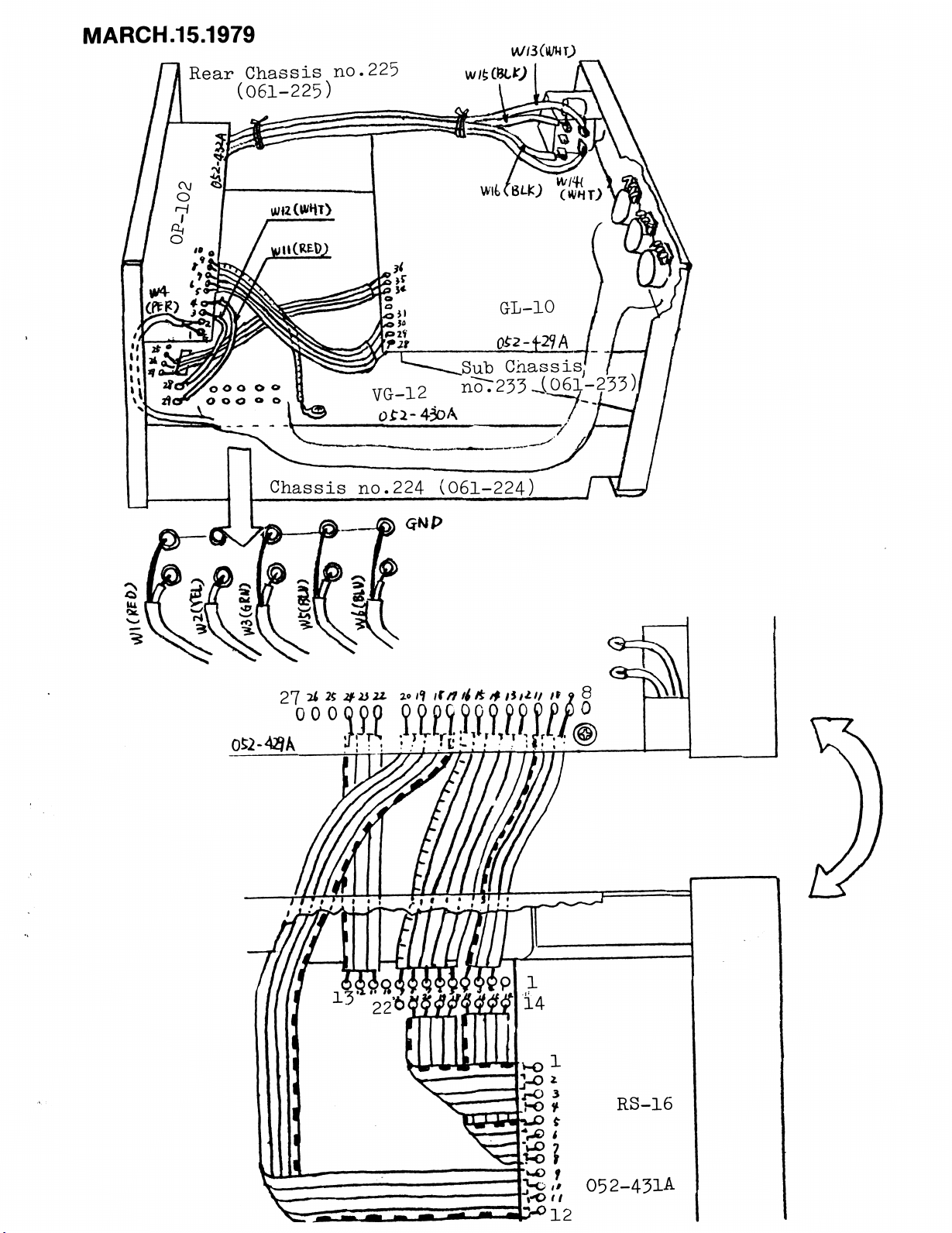
MARCH.15.1979
CR-68
CR-68
SERVICE
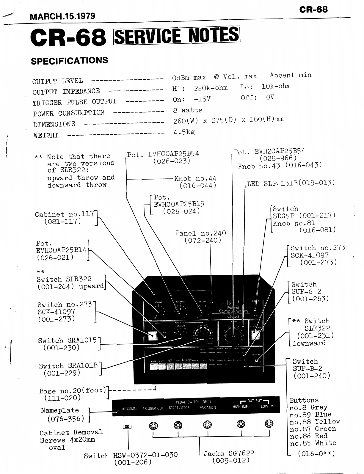
SPECIFICATIONS
OUTPUT
OUTPUT
TRIGGER PULSE
POWER
LEVEL
IMPEDANCE
OUTPUT
CONSUMPTION
DIMENSIONS
WEIGHT
**
Note
are
of
upward
downward
Cabinet
(081-117)
that
two
SLR322:
no.117
there
versions
throw
throw
and
Pot.
NOTES
OdBm
Hi:
On:
8
26O(W)
4.5kg
EVHCOAP25B54
(026-023)
•Knob
Pot.
EVHCOAP25B15
(026-024)
max@Vol.
220k-ohm
+15V
watts
x
no.44
(016-044)
max
Lo:
Off:
275(D)
x
180(H)mm
Pot.
EVH2CAP25B54
Knob no.43
LED
Accent
lOk-ohm
OV
(028-966)
min
(016-043)
SLP-131B(019-013)
Switch
SDG5P
Knob
(OC1-217)
no.81
(016-081)
Pot.
EVHCOAP25B14
(026-021)
*-*
Switch SLR322
(001-264)
Switch
SCK-41097
upward
no.273
(001-273)
Switch
(001-230)
Switch
SRA1015
SRA101B
(001-229)
Base
no.20(foot)~|-
(111-020)J.
Nameplate
(076-356)
Cabinet
Screws
oval
Removal
4x20mm
Switch
HSW-0372-01-030
(001-206)
Jacks
SG7622
(009-012)
'Switch
SCK-41097
no.273
(001-273)
Switch
SUF-6-2
(001-263)
**
Switch
SLR322
(001-231)
.downward
Switch
SUF-B-2
(001-240)
Buttons
no.8
no.89Blue
no.88
no.87
no.86
no.85
L
Grey-
Yellow
Green
Red
White
(016-0**)
Page 2
VK-O0
TEMPO
START
STOP
n
FOOT
START
MANUAL
FOOT
ARI
^TEMPO
J^*^
CLOCK
OSC
BALANCE
BD
CY
HH
M
ONE
SHOT
jxPB
8048
VOICES
ITER
OSC
CONTROL-
|PANEL|SWITh|eS
ACCENT
OUTPUT
IMP
L
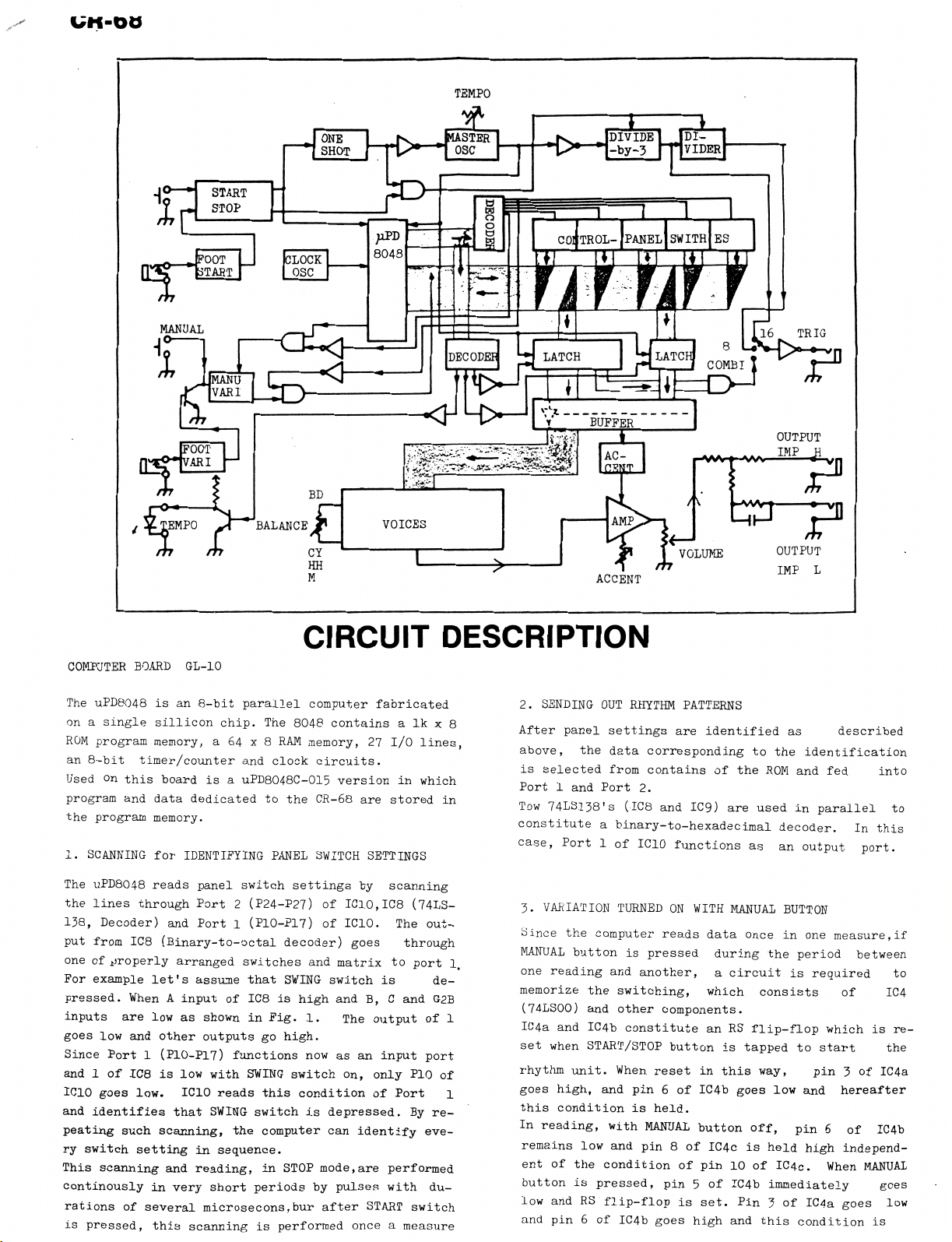
COMPUTER
The
onasingle
ROM
an
Usedonthis
program
the
1.
SCANNING
The
the
138,
put
oneofproperly
For
pressed.
inputs
goes
Since
and1of
IC10
and
peating
ry
switch
This
continouslyinvery
rationsofseveral
is
pressed,
BOARD
uPD8048isan
program
8-bit
and
program
uPD8048
lines
through
Decoder)
from
IC8
example
When A
are
low
and
GL-10
sillicon
memory,
timer/counter
boardisa
data
dedicatedtothe
memory.
for
IDENTIFYING
reads
panel
Port2(P24-P27)ofIC10,IC8
and Port1(P10-P17)ofIC10.
(Binary-to-octal
arranged
let's
assume
inputofIC8ishigh
lowasshown
other
Port1(P10-P17)
IC8islow with
goes
low.
IC10
identifies
such
scanning
that
scanning,
settinginsequence.
and
reading,inSTOP mode,are performed
this
scanningisperformed
CIRCUIT
8-bit
parallel
chip.
a 64 x8RAM
and
uPD8048C-015
switch
switches
that
in Fig.
outputsgohigh.
functions
SWING
reads
this
SWING
switchisdepressed.Byre
the
computer
short
periodsbypulses
microsecons,bur
computer
The
8048
memory,27I/O
clock
circuits.
CR-68
PANEL
SWITCH
settingsbyscanning
decoder)
and
SWING
1.
nowasan input
switch
conditionofPort
fabricated
containsaIkx8
lines,
versioninwhich
are
stored
SETTINGS
(74LS-
The
goes
matrixtoport
switch
andB,C
The
through
is de
and
outputof1
port
on,
only
P10
can
identify
after
START
onceameasure
eve
with
switch
DESCRIPTION
2.
in
out
G2B
of
du
1#
1
SENDING
After
above,
is
selected
Port1and
Tow
74LSl38's
constituteabinary-to-hexadecimal
case,
3.
VARIATION
Since
MANUAL
one
reading
memorize
(74LS00)
IC4a
set
when
rhythm
goes
this
In
reading,
remains
ent of
buttonispressed,
low
andRSflip-flopisset.
and
pin6of
OUT
RHYTHM
panel
settings
the
data
correspondingtothe
from
containsofthe
Port
2.
(IC8
and
Port1of
the
IC10
TURNEDONWITH
computer
buttonispressed
and
another,acircuitisrequired
the
switching,
and
other
and
IC4b
constituteanRS
START/STOP
unit.
When
resetinthis
high,
and
pin6of
conditionisheld.
with
MANUAL
low
and
pin8of
the
conditionofpin10of
IC4b
goes
PATTERNS
are
identified
IC9)
are
as
ROM
described
identification
and
fed
usedinparallel
decoder.Inthis
functionsasan
MANUAL
reads
data
onceinone
during
which
output
BUTTON
the
period
consists
measure,if
of
components.
flip-flop
whichisre
buttonistappedtostart
way,
IC4b
goes
button
pin5of IC4b
high
off,
IC4cisheld
Pin3of
and
this
pin3of IC4a
low
and
hereafter
pin6of
high
independ
IC4c.
immediately
When
IC4a
goes
condition
into
to
port.
between
to
IC4
the
IC4b
MANUAL
goes
low
is
Page 3
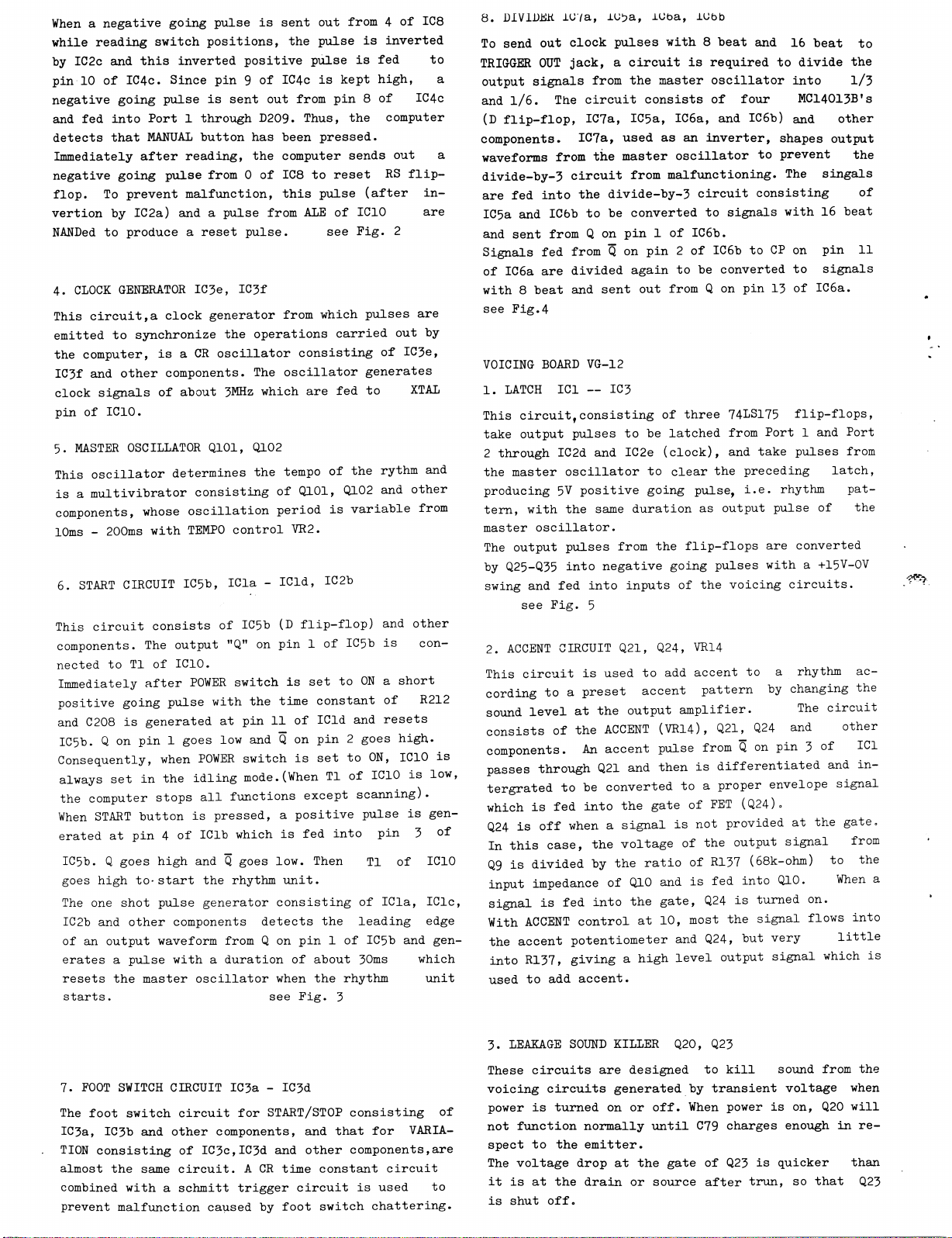
Whenanegative
while
reading
by
IC2c
and
pin10of
negative
and
detects
Immediately
negative
fed
going
into
that
going
flop.Toprevent
vertionbyIC2a)
NANDedtoproduceareset
4.
CLOCK
GENERATOR
This
circuit,a
emittedtosynchronize
the
computer,isaCRoscillator
IC3f
and
other
clock
signalsofabout
pinofIC10.
5.
MASTER
This
oscillator
isamultivibrator
components,
10ms-200ms
6.
START
CIRCUIT
This
circuit
components.
nectedtoTl of
Immediately
positive
and
going
C208isgeneratedatpin11of
IC5b.Qon
Consequently,
always
the
When
setinthe
computer
START
eratedatpin4of
IC5b.Qgoes
goes
high
The
one
shot
IC2b
and
ofanoutput
eratesapulse
resets
starts.
the
going
pulseissent
switch
this
IC4c.
positions,
inverted
Since
pin9of
positive
pulseissent
Port1through
MANUAL
after
button
reading,
pulse
from0of
malfunction,
andapulse
pulse.
IC3e,
IC3f
clock
generator
the
components.
3MHz
OSCILLATOR
Q101,
determines
consisting
whose
oscillation
with
TEMPO
control
IC5b,
ICla-ICld,
consistsofIC5b(Dflip-flop)
The
output
IC10.
after POWER
pulse
pin1goes
when
stops
buttonispressed,apositive
high
to-start
pulse
other
components
waveform
withadurationofabout
master
"Q"onpin1of
switchissettoON a
with
low
POWER
switchissettoON,
idling
andQgoes
oscillator
mode.(WhenTlof
all
functions except
IClb
whichisfed
the
rhythm
generator
fromQon
out
from4of
the
pulseisinverted
pulseisfed
IC4ciskept
out
from pin8of
D209.
Thus,
has
been
pressed.
the
computer
IC8toresetRSflip-
this
pulse
from
ALEofIC10
see
from
which
operations
high,
the
sends
(after
Fig.
pulses
carried
consistingofIC3e,
The
oscillator
which
are fed
Q102
the
tempo
of Q101,
generates
to
of the
Q102
periodisvariable
VR2.
IC2b
IC5b
the
time
constantofR212
ICld
and
andQon
pin2goes
IC10islow,
scanning).
pulseisgen
into
pin3of
low.
Then
unit.
consistingofICla,
detects
pin1of
when
the
see
Pig.
the
3
Tl
leading
IC5b and
30ms
rhythm
IC8
to
a
IC4c
computer
out
a
in-
are
2
are
out
by
XTAL
rythm
and
and
other
from
and
other
is
con
short
resets
high..
IC10
is
of
IC10
IClc,
edge
gen
which
unit
8.
DIVLDEft
To
send
TRIGGER
output
and
1/6.
(D
flip-flop,
components.
waveforms
divide-by-3
are
fed
IC5a
and
sent
Signals
of
IC6a
with8beat
see
Fig.4
VOICING
1.
LATCH
This
take
2
through
the
master
producing5Vpositive
tern,
master
The
output
by
Q25-Q35
swing
2.
ACCENT
This
cordingtoa
sound
consistsofthe
lU'/a, ±u;?a,
out
clock
pulses
OUT
jack,acircuitisrequiredtodivide
signals
into
and
fed
are
BOARD
circuit,consistingofthree
output
with
oscillator.
and fed
see
circuitisusedtoadd
from
the
The
circuit
IC7a,
IC7a,
from
the
circuit
the
IC6b
to be
fromQon
fromQon
divided
and
VG-12
IC1—IC3
pulsestobe
IC2d
and
oscillatortoclear
the
same
pulses
into
into
Fig.
5
CIRCUIT
consistsoffour
IC5a,
usedasan
master
from
divide-by-3
convertedtosignals
pin1of
pin2of
again
sent
out
IC2e
going
durationasoutput
from
negative
inputsofthe
Q21,
preset accent
levelatthe
output
ACCENT
components.Anaccent
passes
tergratedtobe
whichisfed
Q24isoff
In
Q9isdividedbythe
input
signalisfed
With
the
into
usedtoadd
through
Q21
into
whenasignalisnot
this
case,
the
impedanceof010
into
ACCENT
accent
R137,
controlat10,
potentiometer
givingahigh
accent.
and
converted
the
voltageofthe
ratioofR137
the
iCba,
lUbb
with8beat
master
IC6a,
inverter,
and16beat
oscillator
and
IC6b)
shapes
into
MC14O13BTs
and
other
output
oscillatortoprevent
malfunctioning.
circuit
The
singals
consisting
with16beat
IC6b.
IC6btoCPonpin
to be
convertedtosignals
fromQon
latched
(clock),
pulse,
the
flip-flops
going
Q24,
VR14
accenttoa
pin13of IC6a.
74LS175
from
and
the
preceding
i.e.
pulses
voicing
flip-flops,
Port1and
take
pulses
rhythm
pulse
are
converted
witha+15V-0V
circuits,
rhythm
latch,
of
patternbychanging
amplifier.
(VR14),
pulse
Q21,
fromQon
thenisdifferentiated
to a
proper envelope
gateofFET
(Q24).
Q24
pin3of
The
and
circuit
and
signal
providedatthe
output
signal
(68k-ohm)tothe
andisfed
gate,
most
and
level
into
010.
Q24isturned
the
signal
Q24,
but
very
output
signal
When
on.
flows
little
which
to
the
1/3
the
of
11
Port
from
pat
the
ac
the
other
IC1
in-
gate.
from
a
into
is
7.
FOOT
SWITCH
The
foot
IC3a,
IC3b
TION
consistingofIC3c,IC3d
almost the
combined
prevent
malfunction
CIRCUIT
switch
withaschmitt
circuit
and
other
same circuit.ACR
IC3a-IC3d
for
START/STOP
components,
trigger circuitisused
caused
and
and
other
time
by foot
that
constant
switch
consisting
for
components,are
circuit
chattering.
of
VARIA
to
3.
LEAKAGE
These
voicing
poweristurnedonor
not
function
specttothe
The
voltage
itisat
is
shut
SOUND
KILLER
circuits
circuits
off.
are
designedtokill
generatedbytransient
normally
emitter.
dropatthe gateofQ23isquicker
the
drainorsource
Q20,
off.
until
Q23
When
powerison,
C79
charges
after
sound
from
voltage
Q20
enoughinre
trun,sothat
the
when
will
than
Q23
Page 4
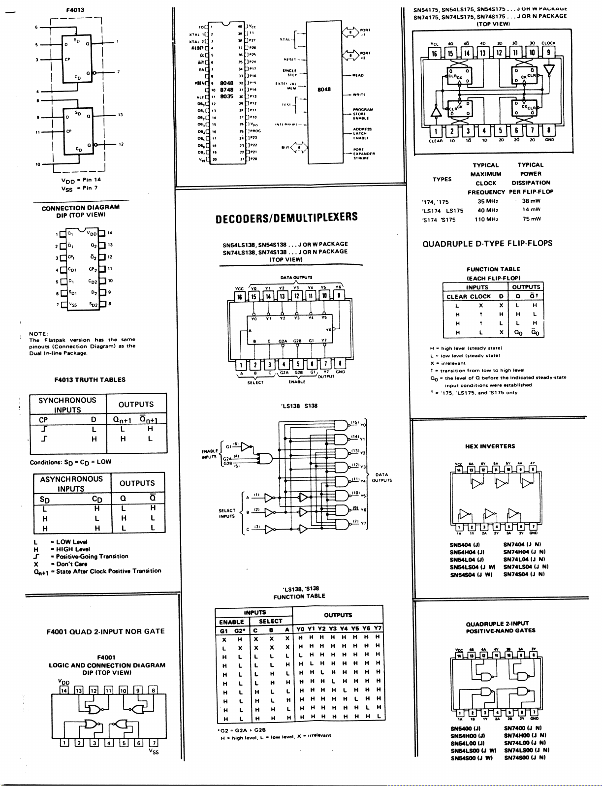
tot
Al
AL
ssC
ml
(AC
AlfC
OB«L
08,
O8,[
iL
ZL
C
t
[
—^y~
9
10
n
17
8048
8748
8035
SN54175.
SN54LS175.
SN74175!
40
39
SN74LS175.
SN54S17b
SN74S175
(TOP
...JOHW
...JORNPACKAGE
VIEW)
KACKAOt
W
»
34
3)
JM6
32
)P14
3»
30
n
i*
7»
CONNECTION
DIP
(TOP
VIEW)
NOTE:
The
Flatpak
pinouts
Dual
version
(Connection
In-line
Package.
F4013
TRUTH
SYNCHRONOUS
INPUTS
CP
S
J"
Conditions:Sq-Cq*
DIAGRAM
CP2
3,0
D2
3'
has
the
Diagram)asthe
same
TABLES
OUTPUTS
D
Qn+1
L
L
H
H
LOW
Qn+1
H
L
oe,C
O8,C
74
71
77
19
7'
20
DECODERS/DEMULTIPLEXERS
SN54LS138.
SN74LS138.
SN54S138
SN74S138
16U15
...JORWPACKAGE
...JORNPACKAGE
(TOP
VIEW)
OATA
OUTPUTS
iinn
SELECT
ENABLE
LS138
S138
MAXIMUM
FREQUENCY
'174/175
'LS174
LS175
'S174
*S175
QUADRUPLE
FUNCTION
(EACH
INPUTS
CLEAR
CLOCK
L
H
H
H
H"high
level
level
input
levelofQ
(steady
(steady
from
conditions
LS175.
HEX
L=low
X**irrelevant
t«transition
Qq-the
T-'175.
TYPICAL
CLOCK
35
MHz
40
MHz
110
MHz
D-TYPE
FLIP-FLOP)
X
t
t
L
state)
state)
lowtohigh
before
were
and
'S175
INVERTERS
TYPICAL
POWER
DISSIPATION
PER
FLIP-FLOP
38
mW
14
mW
75
mW
FLIP-FLOPS
TABLE
OUTPUTS
Q
D
X
H
L
X
the
Qt
L
H
H
L
L
H
Qq
Qo
level
indicated
established
only
steady
state
ASYNCHRONOUS
INPUTS
L
H
H
-
LOW
L
H
S
X
Level
-
HIGH
Level
»
Positive-Going
- Don't
Care
-
State
After
F4001
QUAD
LOGIC
AND
DIP
LU
UJ UJ
OUTPUTS
CD
"IT"
Clock
CONNECTION
L
H
L
L
H
Transition
Positive
2-INPUT
(TOP
F4001
VIEW)
LlJ
LlI Lil LzJ
NOR
H
L
L
Transition
GATE
DIAGRAM
vss
INPUTS
ENABLE
G1
X
L
H
H
H
H
H
H
•G2-G2AfG2B
H=high
C
G2*
xxx
H
XXX
X
L
L
L
L
L
L
L
L
H
L
H
L
H
H
HHL
L
H
L
level.L-
FUNCTION
SELECT
B
L
L
H
H
L
L
H H
low
■LS138.
S138
TABLE
YOY1Y2
A
HHHHHHHH
HHHHHHHH
LHHHHHHH
L
HLHHHHHH
H
HHLHHHHH
L
HHHLHHHH
H
HHHHLHHH
L
HHHHHLHH
H
HHHHHHLH
hhhhhhhl
level.X-
OUTPUTS
Y3 Y4
Y5 Y6
irrelevant
Y7
SN5404
(J)
SN54H04
(J)
SN54L04
(J)
SN54LS04(JW)
SN54S04(JW>
QUADRUPLE
POSITIVE
SN5400
(J)
SN54H00
(J)
SN54L00
(J)
SN54LS00U
SN54S00(JW)
W)
SN74O4(JN)
SN74H04(JN)
SN74L04(JN)
SN74LS04(JN)
SN74S04(JN)
2-INPUT
NANO
QATES
SN7400U
SN74H00U
SN74L00U
SN74LS00U
SN74S00U
GN0
N)
N)
N)
N)
N)
Page 5
MARCH.15.1979
Rear
(061-225)
Chassis
no.225
Chassis
no.224
(061-224)
Sub
Chassis;
n"oT233
^(061-233)
.
Page 6

6(R154)—.
9(R153)—-
3(R156)—
2(R15)
4(R13)
SCOPE
CONNECTION
1
through
013,
014'V
11:
as
illustrated
IN
—
to
CHECK&ADJUSTMENT
The
p|
collector.
H
—
Internal
switch
asagate
going
individual
since
not
computer
switch
MS
is
preferable)
to
pulse
voice
individual
available
respectively.
TRIG-
with
supply
for
pulses
from
EXT.TRIG.
proper
CR-68
(keyboard
serves
negative
triggering
circuit
are
the
time
base
VOICE
to
be
adjusi
BASS
LOW
LOW
HIGH
COW
COW
COW
RIM
CLAVES
MARACAS
HI-HAT
CYMBAL
SNARE
;ed
DRUM
CONGA
BONGO
BONGO
BELL
BELL
BELL
SHOT
DRUM
H
L
Con
nect
scope
to
1
2
3
4
Q13
Q14
5
6
7
8
9
10
11
FREQUENCY
Adjust
VR7
VR5
VR3
VR1
VR9
C
VR10
C
restore
nectiontoprevious
C9
0.676
C4
adjusting
any
one
all
for
ms
16
4.8
2.5
1.66
1.25
1.8
scope
0.38
VR12
voice
62.5
208
400
600
800
555
1,480
2,630
on
makes
Adjust
Hz
shift
•
VOLUME,HIN
I
con-j
!_
DECAY
VR8
VR6
VR4
VR2
scopeVIN
*
*
*
*
*
TIME
for
ms
100
100
40
40
60
5
18
18
50
250
60
AMPLITUDE
■X-
for
V-pp
1.4
Adjust
1.4
0.6
0.7
from
to
Internal
*
*
VR12
VR12
VR12
VR11
1.5
0.5
4.4
0.7
1.5
1.5
1.0
set
BALANCE
at
full-
counter
clockwise
non-
adjustable:
just
full
clockwise
check
"3
1.5V
to
20msec
Figuresinthe
for
personal
tasteorto
ittl
(fair I
Mm
IV
sound
SNARE
table
iv
20msec
pp
:
initiation)
(
only
show
factory
meet
•
s
,<''
after
AMPLITU
standard
and
rDE
may
pvW
]
DECAY
be
frequency'responseofan
mAAa/
i
TIME
slightly
amlifier
deviated
being
used.
Page 7

PT
Black
prim.
White
White
W_hite
Line Cord
Line
Cord
117V
Power
Transformer
(022-124C)
Black
White
White
Power
Transfomer
(022-124D)
220/240V
Terminal
Block
Page 8

CR-68
PARTS
MARCH.15.1979
LIST
081-117
111-020
072-240
076-356
061-224
061-233
061-225
016-043
016-044
016-081
016-008
016-085
016-086
016-087
016-088
016-089
022-030
022-033
022-124NPTno.l24N
022-124CPTno.l24C
Cabinet
Base
Panel
Nameplate
rear
Chassis
Chassis
G-L-10
Chassis
KNOBS
no.43
no.
44
no.
81
Button
COILS&TRANSFORMERS
Coil
Coil
no.117
no.20
no.240
no.356
above
no.224
no.233
mounting
no.225
PUSH
rotary
blk
power
no.8 gray
no.85
no.86
no.87
no.88
no.89
no.30
no.33
022-124DPTno.l24D
(foot)
jacks
main
sub
rear
BUTTONS
TEMPO
switch
white
red
green
yellow
blue
45mH
3R
700mH
100V
117V
220/240V
SWITCHES
001-180
001-273
001-206
001-230
001-229
001-263
001-240
OO1-231*SLR322
001-264*SLR322
026-023
026-024
026-021
028-996
028-001
028-003
028-004
028-005
028-006
032-095
035-109
SDG-5P
SCK-41097
HSW-O372-O1-O3O
SRA1015
SRA101B
SUF-6-2
SUF-B-2
*oposite
POTENTIOMETERS
EVHCOAP25B54
EVHCOAP25B15
EVHC0AP25B14
EVH2CAP25B54
Trimmers
EVTR4AOO(SR19)
EVTR4AOO(SR19)
EVTR4A00(SR19)
EVTR4AOO(SR19)
EVTR4AOO(SR19)
CAPACITORS
0.47uF35VKtant.
ECQM61O3KZ
'
rotary
rotary
push
phsh
lever
lever
throw
50kB
lOOkB
lOkB
50kB
600V
power
keyboard
slide
gang
gang
RHYTHM
AUTO/MANUAL
directions
500-ohm
5k
10k
20k
50k
TRIG
MEASURE
FILL
IN
ROCK—DISCO-2
WALTZ—
A/B
BALANCE
ACCENT
VOLUME
TEMPO
PC
polyester
OUT
PCBs
148-016A
142-010A
143-O12A
149-102
020-141
020-106
020-108
020-138
020-124
020-120 74LS00N
020-169
020-041
179-022
017-106
017-021
017-046
017-016
018-059
018-082
019-013
RS-16A
GL-10A etch
VG-12A
OP-102
ICs
etch
etch
etch
74LS175NorCMOS4O175
7805UC
7815UC
74LS138N
74LS04N
MC14001BCP
MC14013BCP
MPD-8048C-15
TRANSISTORS
2SC1815-GR
2SC900-F
2SC828-R
selected
2SK30A-GR
DIODES
1S1588
regulator
regulator
W-02 bridge
SLP-131B
mask
mask
mask O52-43OA
mask
NZ
for
O52-431A
052-429A
052-432
+5V
+15V
noise
FET
1.5A
LED
FUSES
008-024
008-026
008-056
008-060
012-003
SGA
0.5A
SGA
CEE
CEE
MISCELLANEOUS
Fuse
prim/sec
1A
lOOmAT
25OmAT
Clip
012-040ICSocket
009-012
064-134
047-003
047-023
120-001
053-289
053-290
electrolytic
Jack
SG7622
Holder
Line
Cord
Line
Cord
Long
Nut
Flat
Cable
Flat
Cable
Resistors,
USIC
U2>s^
no.134
no.l
mylars
capacitors
to.
+5V
sec
+15V
prim
sec
TF-758
100/117V
100/117V
220/240V
220/240V
ICC3O-O4O-35OG40pin
line cord
Strain
Clamp 1702B
Relief
3xl0mm stand-off
no.2895pin
no.2904pin
and
everything
the
musician
ordinary
are
omitted.
FOftT
RDA,
Page 9

8048-015
P27
Port
2
74LS138
IC5b
IC5b
IC5b
IC2b
0102
Master
POWER
1
pin
4
CL
pin
3
CP
pin
1
Q
pin
4
collector
Oscillator
Fig.3
ON
r
1
I
START/STO]
ON
.
r
1
I
1
1
1
1
RHYTHM
RHYTHM
y
STARTS
1
i
I
i
I
1
1
i
1
iMaster
i
31
?ART
osc
reset
TIMMINCrDIAGRAM
h'P24
S
TAIt
LT/STOP
1
I
OFF
RHYTHM
I
I
STOPS
L
START/STOPONRHYTHM
IC4a
pin
1
(Reset
IC4b
pulse
Pin
5
M
P17
Port
1
P10
STARTS
i
SWING
t-rl
SCANNING
MATRIX
11
VARIATION
I
Fig.1
ON
II
Y
IC4a
pin
3
i
~
^-rf:
ffO
<0
ft!
§3
= §S
a.
Sec
START/
STOP
IC5a
IC6a
IC6b
IC5a
IC5a
IC5a
IC5a
pin
IC6b
IC5a
pin
IC6b
pin
(16
beat)
ON
pin
pin
8
pin
6
pin
11"
pin
pin
12
13
pin
10
9'
5'
1
MASTER
IRESET
OSC
FREQUENCY
TIMMING
DIAGRAM
Fig.
DIVIDING
4
LTl^LJ
IC4b
IC4c
IC4c
74LS175
IC1orIC2
pin
6
pin 10
pin
8
pin
1
pin
9.
CLOCK
STARTING
VARIATION
WITH
MANUAL
BUTTON
i
Fig.
2
IC6b
IC6a
(8
pin2.
pin
13
beat)
r
L_
FiS.5
RHYTHM
Refertothe
PATTERN
I
I
LATCH
function
table on
page
1
Page 10

vn-uo
GL-10B(142-010B)
VIEW
Serial
from
FOIL
SIDE
No.822000
and
up
Portionsofpattern
shown
Both
correspond
circuit
some
tachedonthe
or
in
on
dated
remain
GL-10A
diagram
components
connectedinseries
the
form
GL-10A
on
unchanged.
and
to
of
and
GL-1OBinplace
GL-1OB
the
since
are
foil
accommo
side
pyramid
not
same
at
CAUTION:
wristbandtoprevent
charge-
RHYTHM
1.
Connect
2.
Turn
Adjust
3.
Turn
Turn
than
rection
4.
Repeat
Always
All
test
TEMPO
scope
TEMPO
TEMPO
YR3
200ms.
knob full
VR1
for
knob
in
the
Stop,
until
steps3and
handle
failureofICs
equipment
ADJUSTMENT
to
Q102
10ms
full
directioninwhich
the
MOS
between
then
periodis200ms.
4.
ICs
while
must
alsobeearth
collector
clockwise
fallorrise
counterclockwise
rotate
VR3 slowlyinthe
wearinganearth
due
to
(Master
(QUICK).
(SLOW).
the
grounded
electrostatic
grounded.
Oscillator).
of
squares.
period
becomes
reverse
shorter
dis
di
S-l
AUTO/MANliL
SLR322
(001-264!
upward
Fla
Cable
#2D
S-2
MEASURE
SRA1015
(001-230)
Switch
SUF-B-2
VARIATION
SRA101B
(001-240
EVH2CAP25B54
966)
Switch
SLR322
downward
(001-231)
131B
-013)
10msec
200msec
(QUICK)
(SLOW)
If
bottom
saturated,
withanew
portionisinsuficiently
replece
pair
of
Q101
the
same
and Q102
rank.
RS-16An48-016A>
Page 11

MARCH.15.1979
CR-68
GL-10
SH0T
GENERATOR
FULSE
MASTER
OSCILLATOR
DECODER
4
2^
clear
clock
2i
clock
if
•
OP-133
Serial
Components
OP-133
•GL-10
and
up.
no.
up
shown
are
located
Serial
no.
to
760899
in
770900
on
TEMPO
r
VARIATION
LATCH
1
SW
RESET
(power
)
MANUAL
VARIATION
RHYTHM
See
below
rhythm
r;
PUSH
for switchi
names
FOX
TROT
TANGO
SW
.
3
RS-16J
&£&
0101
--
104:
D201--248:
IC1
IC2
IC5
IC8
IC10
~
—
--
:
3:
7:
9:
:
J
2SC1815-G-R
1S1588or1S2473
MC14001B
74LS00N
MC14013B
74LS138N
MPD-8048C-015
Page 12

Jacks
1
2
SG7622
(009-012)
SW8
HSW-O372-O1-O3O
VG-12A(143-012A)
OP-102(149-102)
ACCENT
LJ
37
...J
3*
3?
ttfr
42
15
VG
12
OP
2t
-tKT
102
H
IS
22
it
t
GL10
!>
blfi
x>ii
Sl
VARIA1
43
irn
CION
START
STOP
RS16
Page 13

••
•«/•
•«/■«/
So-and
Killer
(power
off)
Sound
Killer
(power
on)
Q2O1
VARIATION
SW7
DISCO-2
01
012
Q22
023
Dl
-
11
-
—
—
_
- 31,
21,
24
025
D1O1
—
2SC900-P
2SC1815-GR
35
2SC828-R(NZ)
2SK30ATM-GR
1S1588or1S2473
noise
Page 14

un-oo
BASS
WALTZ
DRUM
LOW
CONGAIHIGH
T
LOW
Fill
LOW
RHYTHM
BONGO
BONGO
In
CONGA
SNARE
DRUM
PATTERNS
CLAVES
RIM
SHOT
COW
T
MARACAS
BELL
I
HIHAT
I
CYMBAL
ENKA
BOSSA
SAMBA
A
MAMBO
■n
NOVA
■
n
-X.
t
ttf
cm
cha
1 /
T
J
DISCO-l
r
DISCO-2
FILL
__2
IN
i
X_
r
^.
>L
>L
w+rsm
3:
a
SLOW
SWING
FOX
TANGO
&
ROCK
T
TROT
r
r
'
Vf
r
r
zr
BEGUINE
ROCK-l
r
ROCK-2
ROCK-3
^
r
.UJ
Cjr
LI
X7
1(
%J—^rr—«7
RIUMBA
r^-'
r
SE
BOOGIE
ROCK-4
CSTTTT
r
Ur"^
ijjjyj
CT
 Loading...