

Page 1
Table of Contents
AD-10Sep. 2017
SERVICE NOTES
Issued by RJA
Cautionary Notes ..............................................................2
Specifications .....................................................................3
Location of Controls .........................................................4
Location of Controls Parts List........................................5
Exploded View ..................................................................6
Exploded View Parts List.................................................7
Disassembly Procedure....................................................7
Plain View ..........................................................................8
Plain View Parts List.........................................................8
Block Diagram/Wiring Diagram..................................10
Parts List...........................................................................12
Verifying the Version......................................................14
Data Backup and Restore Operations ..........................14
Performing a Factory Reset............................................14
Updating the System ......................................................14
Test Mode.........................................................................15
Circuit Board (Main Board) ...........................................18
Circuit Diagram (Main Board: 1/3)..............................20
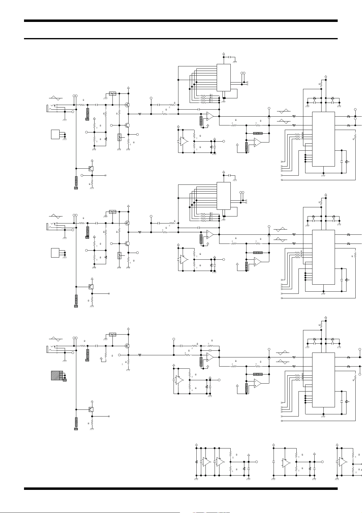
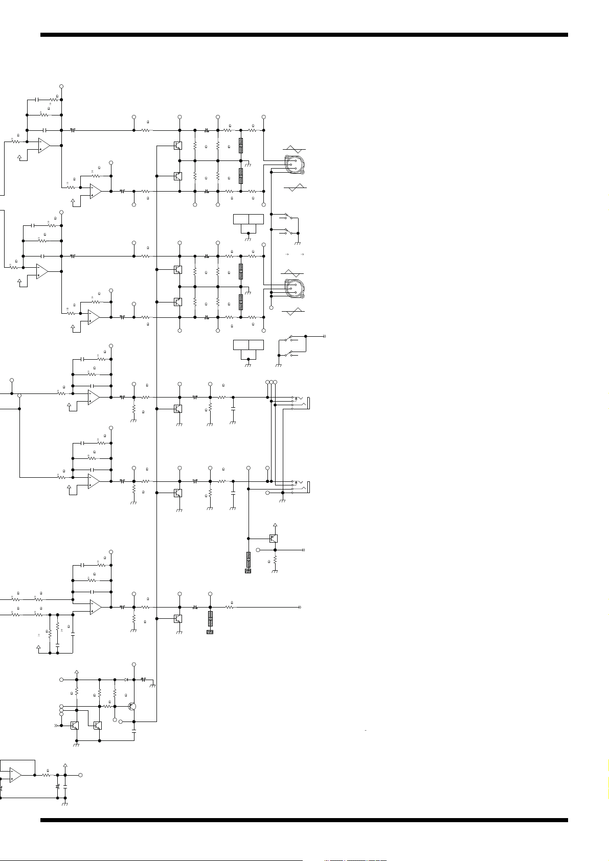
Circuit Diagram (Main Board: 2/3)..............................22
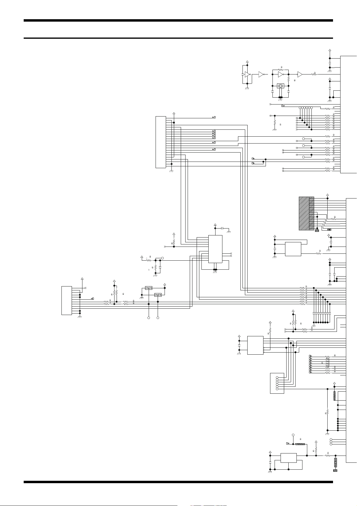
Circuit Diagram (Main Board: 3/3)..............................24
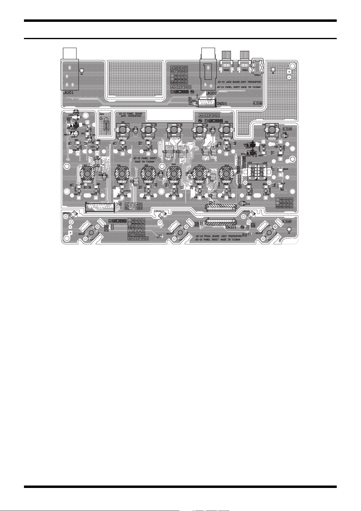
Circuit Board (Panel, Jack, Pedal Board) .....................26
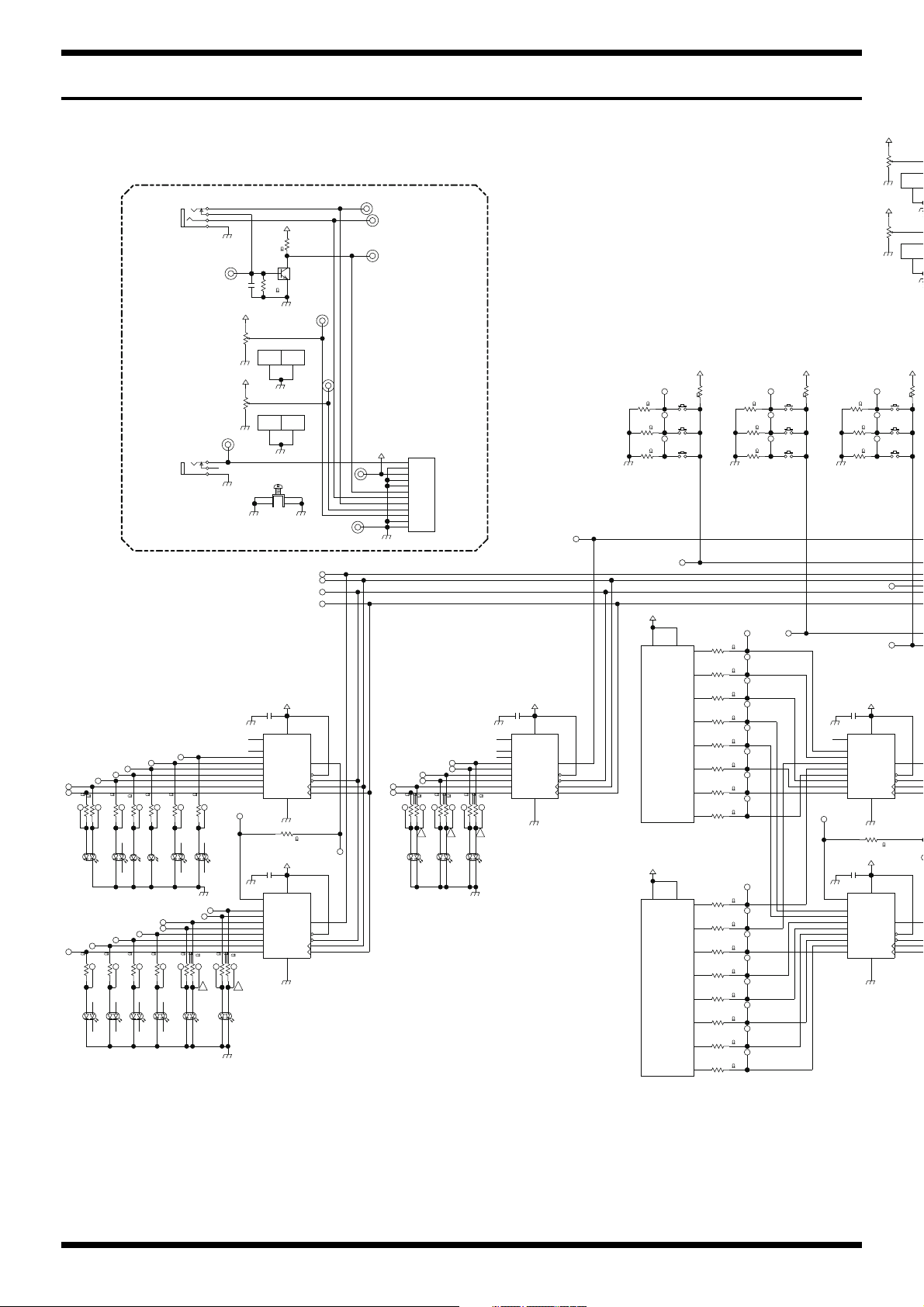
Circuit Diagram (Panel, Jack, Pedal Board) ................28
Copyright © 2017 Roland Corporation
All rights reserved. No part of this publication may be reproduced in any form without the written permission
of Roland Corporation.
CC-KWS17057129E0
Page 2

Sep. 2017 AD-10
Cautionary Notes
Before beginning the procedure, please read
through this document. The matters described may
differ according to the model.
Back Up User Data!
User data may be lost during the course of the procedure. Refer to Data
Backup and Restore Operations (p. 14) in the Service Notes and save the
data. After completing the procedure, restore the backed-up data to the
product.
Part Replacement
When replacing components near the power-supply circuit or a heatgenerating circuit (such as a circuit provided with a heat sink or including a
cement resistor), carry out the procedure according to the instructions with
respect to the part number, direction, and attachment position (mounting so as
to leave an air gap between the component and the circuit board, etc.).
Parts List
A component whose part code is ******** will not be supplied as a service part
because one of the following reasons applies.
• Because it is supplied as an assembled part (under a different part code).
• Because a number of circuit boards are grouped together and supplied as
a single circuit board (under a different part code).
• Because supply is prohibited due to copyright restrictions.
• Because reissuance is restricted.
• Because the part is made to order (at current market price).
• Because it is carried in electronic data on the Roland web site.
• Because it is a package or an accessory irrelevant to the function
maintenance of the main body.
• Because it can be replaced with an article on the market. (battery or etc.)
Circuit Diagram
In the circuit diagram, “NIU” is an abbreviation for “Not in Use,” and
“UnPop” is an abbreviation for “Unpopulated.” They both mean non-mounted
components. The circuit board and circuit board diagram show silk-screened
indications, but no components are mounted.
There are cases that the circuit diagrams are omitted. This omission will
happen to the highly integrated digital circuit boards (e.g. Main Board etc) that
are virtually impossible to repair nor analyze.
Roland Japan Warranty
Please send the problem report with followings when the defect occurred
within one year from production and within one month from the first
customer’s purchase.
• Model name:
• Serial number:
•Version:
• Purchase date by the first customer: yyyy/mm/dd
•Symptom:
• Frequency: always, sometimes or seldom
• Confirmed the symptom at your service dept: Yes/No
Please send the problem report to [email protected].
2
Page 3

Specifications
BOSS AD-10: Acoustic Preamp
AD-10Sep. 2017
Nominal Input Level
GUITAR IN 1,2: -10 dBu (Adjustable)
RETURN: -10 dBu
Input Impedance
GUITAR IN 1,2: 10 MΩ
RETURN: 220 kΩ
Nominal Output Level
SEND: -10 dBu
LINE OUT L/PHONES, R/MONO: -10 dBu
XLR OUT L, R: -10 dBu
Output Impedance
SEND: 1 kΩ
LINE OUT L/PHONES, R/MONO: 44 Ω
XLR OUT L, R: 600 Ω
Mode
Manual
Memory
Number of Memory
10
Power Supply
AC adaptor
Alkaline battery (AA, LR6) x 6
Current Draw
300 mA
Expected battery life under continuous use
Alkaline battery: Approx. 6 hours
* These figures will vary depending on the actual conditions of use.
Dimensions
217 (W) x 161 (D) x 65 (H) mm
8-9/16 (W) x 6-3/8 (D) x 2-9/16 (H) inches
Weight
1.3 kg (including batteries)
2 lbs 14 oz (including batteries)
Accessories
Owner’s Manual (#5100057809)
Leaflet “USING THE UNIT SAFELY” (#********)
AC adaptor (#********)
Effects
ACOUSTIC RESONANCE (3Type)
COMP (2Type)
4 BAND EQ, LOW CUT
BOOST
CHORUS (3Type)
DELAY (3Type)
REVERB (3Type)
ANTI-FEEDBACK (REDUCTION, NOTCHx2)
Phrase Loop
80 sec
Display
7 segments, 2 digits LED
Connectors
GUITAR IN 1,2 jack: 1/4-inch phone type
SEND: 1/4-inch phone type
RETURN: 1/4-inch phone type
XLR OUT L, R connectors: XLR type
LINE OUT L/PHONES, R/MONO jacks: 1/4-inch phone type
EXP/CTL1,2 jack: 1/4-inch TRS phone type
USB COMPUTER port: USB type B
DC IN jack
Options (sold separately)
Expression Pedal: EV-30, FV-500H/L, Roland EV-5
Footswitch: FS-5U
Dual Footswitch: FS-6, FS-7
* 0 dBu = 0.775 Vrms
* Printed matters will not be supplied after the end of the production. Then,
download the electronic file from the Roland web site.
* In the interest of product improvement, the specifications and/or appearance of
this unit are subject to change without prior notice.
3
Page 4
Sep. 2017 AD-10
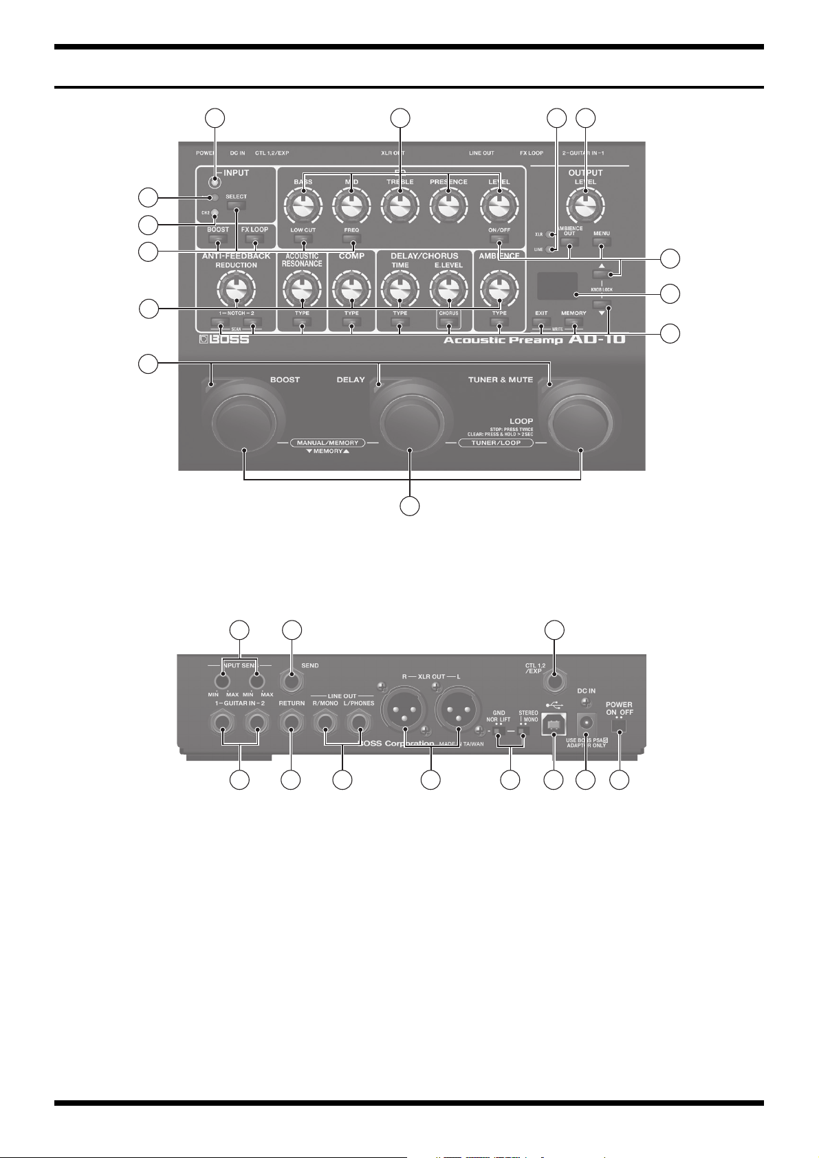
Location of Controls
fig.panel.eps
1 24 4
2
3
5
6
7
8
109 17
5
6
5
4
1816
13 14 1517 11 12
Page 5

Location of Controls Parts List
No. Part Code Part Name Description Q’ty
1 5100049857 LED OSRGHC3132A 1
5100024412 LED SPACER LED3X6.5 1
2 05015956 LED BL L-7104SRT (F5229820R0) 3
5100037402 LED SPACER LEDS-7.5S 3
3 05015967 LED L-7104SGT 1
5100037402 LED SPACER LEDS-7.5S 1
4 5100001453 ROTARY POTENTIOMETER RD901F-40-125F-B50K-0CD 6
03344934 R-KNOB (75D522N0R0) 6
******** VR NUT M7 attached to VR 6
5 5100055451 SWITCH EVPAWCD4A 19
5100057242 S-KEYTOP SD 19
6 5100037380 ROTARY POTENTIOMETER RV09BDF-40E1-125F-B50K-00D 6
03344934 R-KNOB (75D522N0R0) 6
******** VR NUT M9 attached to VR 6
7 5100049511 SWITCH PEDAL LED LENS 3
5100050548 THERMAL SHRINKAGE TUBE 15X10.0 3
8 5100049826 SWITCH SKPFACA010 3
5100050211 SWITCH PEDAL RING 3
5100049509 SWITCH PEDAL 3
5100050359 SWITCH PEDAL FOOT 3
5100050360 PEDAL SPRING 3
5100049510 SWITCH PEDAL ESCUTCHEON 3
9 5100047382 ROTARY POTENTIOMETER RV09AF-21-15K-B50K 2
10 5100001342 6.5MM JACK HTJ-064-12IMP (13449155R1) 1
11 5100057969 XLR CONNECTOR CT3-05M-EP 2
12 5100011813 SWITCH (F3159712R0) SV69010F-0202-6V-NP-001 2
13 5100007092 USB CONNECTOR UBR24-4K5J00(F3439908R0) 1
14 04908712 DC JACK KM02020ABM2P (F3439892R0) 1
5100042085 DC JACK HOLDER 1
15 5100031222 SWITCH (F3159716R0) SV71010F-0202-6T-NP 1
16 5100034719 6.5MM JACK HTJ-064-22HSPP 2
5100002917 JACK COVER L 2
17 5100034719 6.5MM JACK HTJ-064-22HSPP 1
18 5100034719 6.5MM JACK HTJ-064-22HSPP 2
AD-10Sep. 2017
5
Page 6
Sep. 2017 AD-10
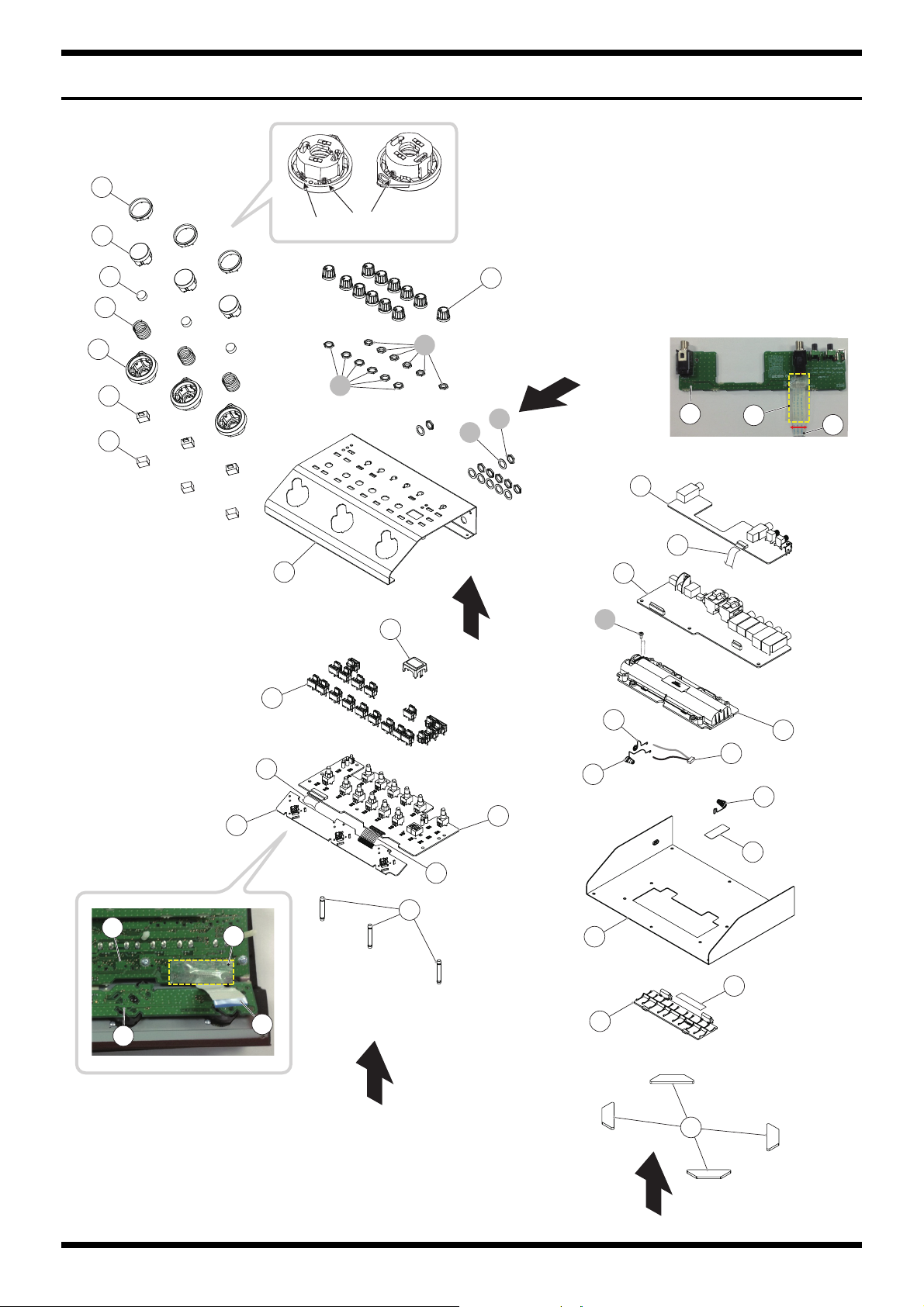
Exploded View
fig.bunkai-e.eps
2
3
4
5
6
7
8
* Apply adhesive (#40122445).
d
e
9
10
c
View 4
1
View 1
b
14
15
a
18
14
30
18
12
13
13
30
16
16
11
View 3
19
17
12
22
25
28
21
20
24
23
26
27
29
6
View 2
Page 7
Exploded View Parts List
No. Part Code Part Name Description Q’ty
1 03344934 R-KNOB (75D522N0R0) 12
2 5100050211 SWITCH PEDAL RING 3
3 5100049509 SWITCH PEDAL 3
4 5100050359 SWITCH PEDAL FOOT 3
5 5100050360 PEDAL SPRING 3
6 5100049510 SWITCH PEDAL ESCUTCHEON 3
7 5100049511 SWITCH PEDAL LED LENS 3
8 5100050548 THERMAL SHRINKAGE TUBE 15X10.0 3
9 5100057241 TOP COVER 1
10 5100049507 7-SEG COVER 1
11 5100057242 S-KEYTOP SD 19
5100056291 PANEL SHEET ASSY 1
* This unit includes the following parts.
12 ******** PANEL BOARD 1
13 ******** PEDAL BOARD 1
14 ******** JACK BOARD 1
17 5100058463 RIBBON CABLE 12P L=40X6X6 P=2.0 1
15 5100056290 MAIN BOARD ASSY 1
16 5100050563 FLAT CABLE SML2CD-22X60-BDX6(BL)-P1.0-S4 1
18 5100043624 FLAT CABLE SML2CD-12X52-BDX5(BL)-P1.0-S4 1
19 5100050362 PWB SPACER LCC-25 3
20 5100008058 TWIN BATTERY CASE V6 (G2017620R0) 1
21 5100008059 BATTERY TERMINAL (+) (G2177308R0) 1
22 5100008061 BATTERY TERMINAL (-) 1
23 5100008060 BATTERY TERMINAL (+-) (G2177307R2) 1
24 5100007871 WIRING L=80MM 2P (G3487163R0) 1
25 5100049506 BOTTOM CASE 1
26 5100008057 BATTERY INSULATING SHEET (G2257130R0) 1
27 5100050373 BATTERY LABEL 1
28 5100008056 BATTERY COVER (G2017621R0) 1
29 5100042662 FOOT 4
30 5100005300 FILAMENT TAPE 3M #898 W20MM -
AD-10Sep. 2017
a 5100008243 SCREW 2.6X5 (H5019430R0) BINDING TAPTITE P FEZC 2
b 5100003918 JACK NUT M9X12X2 NI RTC(H5039510R0) 7
c 5100003926 PLAIN WASHER 9X13.5X0.5T NI(H5039158R0) 7
d ******** VR NUT M7 attached to VR 6
e ******** VR NUT M9 attached to VR 6
Disassembly Procedure
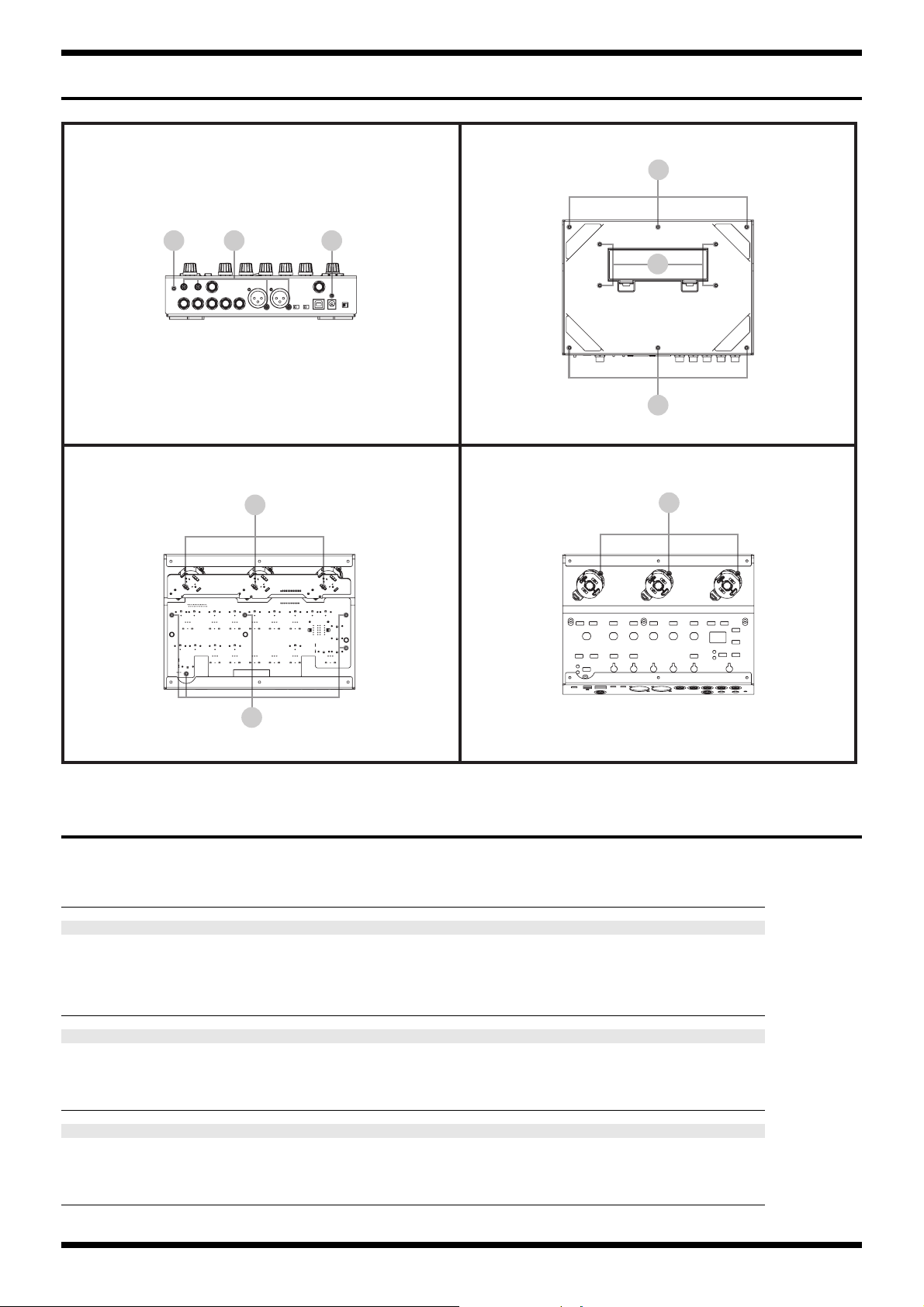
1. Remove screws (x 6) securing the Bottom Case from underneath. (Plain
View (p. 8), a in View 2)
2. Lift the Bottom Case gently and disconnect the battery wiring from the
circuit board.
3. Detach the Bottom Case.
7
Page 8
Sep. 2017 AD-10
Plain View
fig.heimen.eps
View 1 View 2
b
ac
View 3 View 4
e
a
e
a
g
d
Plain View Parts List
View 1
No. Part Code Part Name Description Q’ty
a 40012534 SCREW 3X6 BINDING TAPTITE S FE BZC 1
b 5100036736 SCREW 2.9X9 BINDING TAPTITE B SERRATE BZC 4
c 40342712 SCREW M3X6 PAN MACHINE W/SW+SMALL PW BZC 1
View 2
No. Part Code Part Name Description Q’ty
a 40012534 SCREW 3X6 BINDING TAPTITE S FE BZC 6
e 40011301 SCREW 3X6 BINDING TAPTITE P FE BZC 4
View 3
No. Part Code Part Name Description Q’ty
d 40017934 SCREW M3X6 PAN MACHINE W/SW+PW(L) FE ZC 5
e 40011301 SCREW 3X6 BINDING TAPTITE P FE BZC 3
View 4
No. Part Code Part Name Description Q’ty
g 5100008243 SCREW 2.6X5 (H5019430R0) BINDING TAPTITE P FEZC 3
8
Page 9

AD-10Sep. 2017
9
Page 10
Sep. 2017 AD-10
IC2
DC-DC
D+1.2
D+3.3
CH1
CH2
CH3
FB4.9
Reg
JK7
GUITAR 1
JK2
GUITAR 2
JK3
RETURN
F1
FOR PSA-**S
(9.65-8.55V)
Q7
MOS-FET
CN1
PVCC
MUTE Ctrl
MAIN BOARD
JK9 USB
FUNCTION
CN
4
JTAG
D+3.3
CKCPU
IC
48MHz
Serial Flash
SFI
D+3.3
_RESET
RESET
X1
16.9344MHz
XTAL
Buffer
NJM2115
Pre-Em
A+3.3
A+3.3
MUTE DTr
MUTE DTr
2SK880
buffer
AVCC
IC17
CODEC
(AK4556)
A+3.3
IC15
NJM4580
De-Em
AVCC-PHONES
MUTE DTr
MUTE DTr
IC19
CODEC
(AK4556)
A+3.3
MUTE DTr
D+3.3
D+3.3
IC20
ESC2
UD
D+3.3
VDE
D+1.2
VDD
IC6
W-RAM
(64Mbit)
MA(1 5:0)
M
D(
1
5:
0
)
EA(
1
4:0)
IC5
E-RAM
(256Mbit)
AIN 0:1
ED(1
5
:0
)
AIN 4:7
PB7
TRCD0-3/DRCCKO
TRST/TCK,SWCLK/SMS,SWDIO/TDI/TDO,SWV
SFICKO/SFICSO/SFIDIN/SFIDO/_SFIHLD
CKUDL
NJM4580
De-Em
AVCC
ripple
ripple
filter
AVCC
AVCC-PHONE
port
SDDA1
SDAD1
SDDA2
SDAD2
SDDA0
SDAD0
L
R
CK
M
CK
B
C
K
XCODEC-
P
DN
SDDA0-2
SDAD0-2
J
2,K
1,
H
1
,
K
2
H2,J 1,L 1,
N
1,
M1
por
t
XOFF_PWR
XSWD_PWR
AIN2,3
PF12/PF15
BUDO0,1,2/BUCK
BULCK/PA0
ADMPX0,1
AVCC
2SK880
buffer
A+3.3
NJM2115
AFAD
IC18
CODEC
(AK4556)
IC10
NJM4580
De-Em
AVCC
IC3
NJM4580
De-Em
NJM2115
Pre-Em
A+3.3
A+3.3
NJM2115
AFAD
2SK880
buffer
AVCC
NJM2115
Pre-Em
A+3.3
A+3.3
NJM2115
AFAD
JK1
DC IN
SW2
POWER
port
Multiplexer
(GAIN ctl)
Multiplexer
(GAIN ctl)
p
o
r
t
AF+3.3
Reg
p
o
r
t
port
po
r
t
port
p
ort
AA, LR6 x 6
RTN
DET
GTR2
DET
GTR1
DET
1
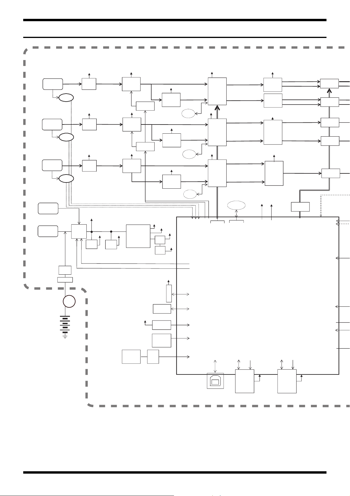
Block Diagram/Wiring Diagram
fig.block.eps@L
10
Page 11
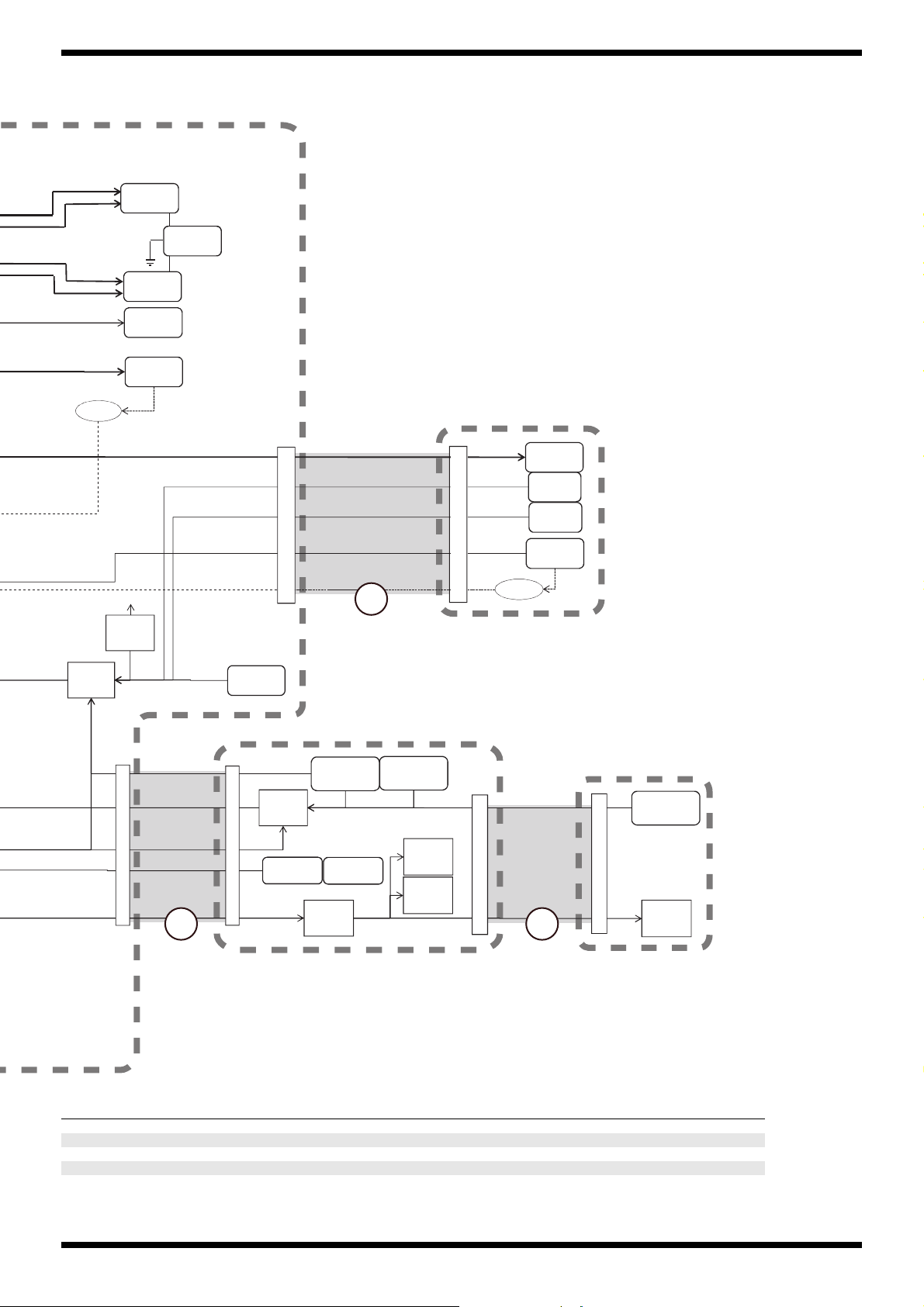
fig.block.eps@R
Panel SW
VR201
JK8
L/PHONES
JK5
XLR OUT R
PANEL
BOARD
PEDAL
BOARD
JACK BOARD
8bit Shift
×7
Multiplexer
×2
LED
CTL-TIP/RING
PVCC
BATTERY
MONITOR
Circuit
AIN2
to MPX
to 8bit shift
JK6
XLR OUT L
SW1
GND LIFT
JK202
SEND
JK4
R/MONO
JK201
CTL/EXP
SW3
STEREO/MON
VR202
VR
Foot LED
×9
7SEG
×2
Foot SW
Multiplexer
OUTR DET
SW16
CN2
CN2
C
N
1
CN101
CTL DET
CN7
CN201
SW17
2
3 4
AD-10Sep. 2017
No. Part Code Part Name Description Q’ty
1 5100007871 WIRING L=80MM 2P (G3487163R0) 1
2 5100043624 FLAT CABLE SML2CD-12X52-BDX5(BL)-P1.0-S4 1
3 5100050563 FLAT CABLE SML2CD-22X60-BDX6(BL)-P1.0-S4 1
4 5100058463 RIBBON CABLE 12P L=40X6X6 P=2.0 1
11
Page 12
Sep. 2017 AD-10
Parts List
fig.-part1-e.eps
Safety Precautions:
The parts marked have
safety-related characteristics. Use
only listed parts for replacement.
Note: The parts marked # are new. (initial parts) The description “Q’ty” means a necessary number of the parts per one product.
CASING
# 5100057241 TOP COVER 1
KNOB, BUTTON
# 5100057242 S-KEYTOP SD 19
SWITCH
# 5100055451 SWITCH EVPAWCD4A 19
5100049507 7-SEG COVER 1
5100049509 SWITCH PEDAL 3
5100049510 SWITCH PEDAL ESCUTCHEON 3
5100049511 SWITCH PEDAL LED LENS 3
5100049506 BOTTOM CASE 1
5100008056 BATTERY COVER (G2017621R0) 1
5100008058 TWIN BATTERY CASE V6 (G2017620R0) 1
03344934 R-KNOB (75D522N0R0) 12
5100011813 SWITCH (F3159712R0) SV69010F-0202-6V-NP-001 2
5100031222 SWITCH (F3159716R0) SV71010F-0202-6T-NP 1
Due to one or more of the following reasons, parts with parts code ******** cannot be supplied
as service parts.
• Supply is prohibited due to copyright restrictions.
• It is carried in electronic data on the Roland web site.
• The part is made to order (at current market price).
• It can be replaced with an article on the market. (battery or etc.)
• It is a package or an accessory irrelevant to the function maintenance of the main body.
• A number of circuit boards are grouped together and supplied as a single circuit board (under a different part code).
• Reissuance is restricted.
• It is supplied as an assembled part
(under a different part code).
JACK, EXT TERMINAL
# 5100057969 XLR CONNECTOR CT3-05M-EP 2
SPEAKER, BUZZER
PWB ASSY
# 5100056290 MAIN BOARD ASSY 1
# 5100056291 PANEL SHEET ASSY 1
DIODE
POTENTIOMETER
5100034719 6.5MM JACK HTJ-064-22HSPP 6
5100001342 6.5MM JACK HTJ-064-12IMP (13449155R1) 1
04908712 DC JACK KM02020ABM2P (F3439892R0) 1
5100007092 USB CONNECTOR UBR24-4K5J00(F3439908R0) 1
5100049826 SWITCH SKPFACA010 3
* This unit includes the following parts.
******** PANEL BOARD 1
******** JACK BOARD 1
******** PEDAL BOARD 1
05015956 LED BL L-7104SRT (F5229820R0) 3
05015967 LED L-7104SGT 1
5100049700 LED OSK10303-IRA 2
5100049857 LED OSRGHC3132A 1
5100001453 ROTARY POTENTIOMETER RD901F-40-125F-B50K-0CD 6
5100047382 ROTARY POTENTIOMETER RV09AF-21-15K-B50K 2
5100037380 ROTARY POTENTIOMETER RV09BDF-40E1-125F-B50K-00D 6
WIRING, CABLE
# 5100058463 RIBBON CABLE 12P L=40X6X6 P=2.0 1
5100007871 WIRING L=80MM 2P (G3487163R0) 1
5100043624 FLAT CABLE SML2CD-12X52-BDX5(BL)-P1.0-S4 1
5100050563 FLAT CABLE SML2CD-22X60-BDX6(BL)-P1.0-S4 1
12
Page 13
AD-10Sep. 2017
SCREWS
40017934 SCREW M3X6 PAN MACHINE W/SW+PW(L) FE ZC 5
40342712 SCREW M3X6 PAN MACHINE W/SW+SMALL PW
BZC
5100008243 SCREW 2.6X5 (H5019430R0) BINDING TAPTITE P FEZC 5
5100036736 SCREW 2.9X9 BINDING TAPTITE B SERRATE BZC 4
40011301 SCREW 3X6 BINDING TAPTITE P FE BZC 7
40012534 SCREW 3X6 BINDING TAPTITE S FE BZC 7
5100003918 JACK NUT M9X12X2 NI RTC(H5039510R0) 7
5100003926 PLAIN WASHER 9X13.5X0.5T NI(H5039158R0) 7
MISCELLANEOUS
5100008057 BATTERY INSULATING SHEET (G2257130R0) 1
5100008059 BATTERY TERMINAL (+) (G2177308R0) 1
5100008061 BATTERY TERMINAL (-) 1
5100008060 BATTERY TERMINAL (+-) (G2177307R2) 1
5100042085 DC JACK HOLDER 1
5100042662 FOOT 4
5100002917 JACK COVER L 2
5100050362 PWB SPACER LCC-25 3
5100037402 LED SPACER LEDS-7.5S 4
5100024412 LED SPACER LED3X6.5 1
5100050360 PEDAL SPRING 3
5100050359 SWITCH PEDAL FOOT 3
5100050211 SWITCH PEDAL RING 3
5100050548 THERMAL SHRINKAGE TUBE 15X10.0 3
5100050373 BATTERY LABEL 1
5100005300 FILAMENT TAPE 3M #898 W20MM 40122445 ADHESIVE CEMEDINE SUPER-X NO.8008 170G/135ML -
ACCESSORIES (Standard)
# 5100057809 OWNER’S MANUAL MULTILANGUAGE 1
******** AC ADAPTOR PSA-100S2 for 100V 1
******** AC ADAPTOR PSA-120S2 for 117VU, 117VU/CS 1
******** AC ADAPTOR PSA-120ZS2 for 117VBL 1
******** AC ADAPTOR PSA-230S2 for 230VEU 1
******** AC ADAPTOR PSA-230ES2 for 230VE 1
******** AC ADAPTOR PSA-240S2 for 240VA 1
******** AC ADAPTOR PSA-220CS2 for 220VCNR 1
******** AC ADAPTOR PSA-220KS(R) for 220VK 1
1
* AC adaptors that part codes are indicated as ******** are not supplied. Please purchase an article.
13
Page 14
Sep. 2017 AD-10
01
6789
2
34 5
A.B
Verifying the Version
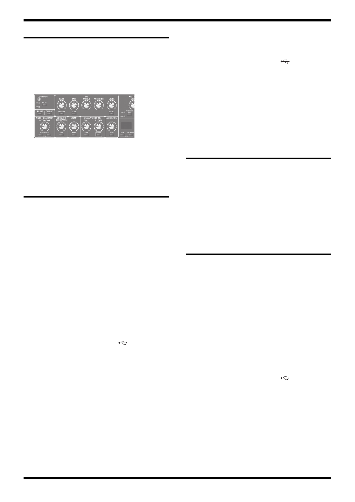
1. Hold down EXIT and MEMORY at the lower right of the panel and turn
on the power.
The display of the 7-segment LED display and the lighting of the buttons
indicate the version.
A.B: Indicates the values of the integer portion and the first
decimal place.
0 through 9: The number corresponding to the lighting button indicates
the value of the second decimal place.
fig.version.eps
(Example) When A is 1, B is 0 and ON/OFF in the EQ section lights up,
the version is 1.02.
2. Turn off the power.
Data Backup and Restore Operations
Items Required
•Computer
• AC adaptor (PSA-series device)
•USB cable
Data Restore Operations
1. Connect the AC adaptor to the AD-10, and hold down MEMORY and
CHORUS in the DELAY/CHORUS section and turn on the power.
bu appears on the 7-segment LED display.
2. Connect the computer to the USB connector ( ).
MEMORY flashes.
3. Start the MIDI sequence program on the computer, and set the MIDI
output device to the AD-10, and send the SysEx data which has been
saved.
rH (rX) appears on the 7-segment LED display and XLR in the OUTPUT
section flashes.
When the receiving is completed, bu appears on the 7-segment LED
display and MEMORY flashes.
4. Quit the MIDI sequence program and detach the USB cable.
5. Turn off the power to the AD-10.
Performing a Factory Reset
1. Hold down NOTCH 1 and NOTCH 2 in the ANTI-FEEDBACK section
and turn on the power.
Fr appears on the 7-segment LED display and MEMORY flashes.
2. To execute the factory reset, press MEMORY. To cancel it, turn off the
power.
When MEMORY is pressed, the 7-segment LED display flashes and the
factory reset is executed.
* Never switch off the power while the Factory Reset operation is in progress.
When ok appears, the factory reset has finished.
3. Turn off the power.
• MIDI sequence program (MIDI-OX, Cakewalk Sonar LE or etc.)
* Install these to the computer above.
* MIDI-OX is available at the following website.
http://www.midiox.com/
•USB driver
* Obtain this from the following website and install it on the computer above.
https://www.roland.com/global/
Data Backup
1. Connect the AC adaptor to the AD-10, and hold down MEMORY and
CHORUS in the DELAY/CHORUS section and turn on the power.
bu appears on the 7-segment LED display.
2. Connect the computer to the USB connector ( ).
MEMORY flashes.
3. Start the MIDI sequence program on the computer, and set the MIDI
input device to the AD-10, and let the system standby for receiving SysEx
data.
4. Press MEMORY of the AD-10.
tH (tX) appears on the 7-segment LED display and XLR in the OUTPUT
section flashes, then the data is sent to the MIDI sequence program.
When the sending is completed, ok appears on the 7-segment LED
display and MEMORY lights up.
5. Save the received SysEX data on the MIDI sequence program.
6. Quit the MIDI sequence program and detach the USB cable.
7. Turn off the power to the AD-10.
Updating the System
Items Required
•Computer
• AC adaptor (PSA-series device)
•USB cable
• Update program (obtained via Service Net)
* The update program is made up of the following two files.
AD_10_UPD.BIN
ROMINFO.TXT
Procedure
1. Copy the update program to any folder on the computer.
2. Connect the AC adaptor to the AD-10, and hold down EXIT and
MEMORY and turn on the power.
The display of the 7-segment LED display and the lighting of the buttons
indicate the version.
3. Connect the computer to the USB connector ( ).
PC appears on the 7-segment LED display and the AD10UPD drive
appears on the screen of the computer.
4. Copy the update program (2 files described above) to the root folder of
the AD10UPD drive.
5. End the USB connection and disconnect the USB cable.
MEMORY of the AD-10 flashes.
6. Press MEMORY.
ud appears on the 7-segment LED display and 10 buttons from EQ LOW
CUT to AMBIENCE TYPE flash, and the update starts. As the update
proceeds, 10 buttons change to lighting in sequence from the upper left.
14
Page 15
AD-10Sep. 2017
47k
* Never switch off the power or detach the plug of the AC adaptor while the update
is in progress.
When 10 buttons all light up and ok is displayed on the 7-segment LED
display, the update has finished.
7. Turn off the power.
Test Mode
Items Required
•Computer
• USB Cable (Type A <-> type B)
• AC adaptor (PSA-series device)
• Oscillator
• Oscilloscope
•Noise meter
•Tester
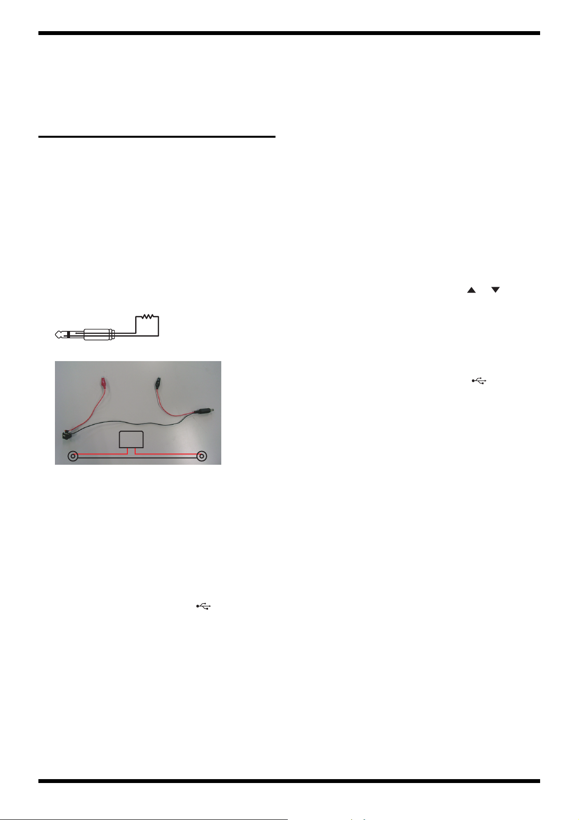
• Expression pedal (EV-5 or EV-30)
* Adjust the minimum volume knob to 0.
• 1/4-inch monaural phone plug with 47-kΩ load resister (x 3)
fig.47k-dummy-plug.eps
• Current-consumption measurement tool
fig.test-check-cable.eps
Quitting the Test Mode
Turn off the power.
Test Items
1. Device Check (p. 15)
2. Version Check (p. 16)
3. Measurement of Current Consumption (p. 16)
4. Switch and LED check (p. 16)
5. Volume Check (p. 16)
Sh Expression Pedal Check (p. 17)
SA Audio Check (p. 17)
SA Noise check (p. 17)
The following test item is executed in the normal mode.
GND LIFT Check (p. 17)
* The test items indicated with 6–8 on the 7-segment LED display are not used for
servicing.
Executing or Skipping Test Items
1. With the 7-segment LED display flashing, press or to select a
test item and press MEMORY, then the test item which number is flashing
can be executed.
While execution of the test item is in progress, when EXIT is held down
and MEMORY is pressed, the 7-segment LED display begins flashing as
above.
1. Device Check
* Before entering this test item, connect the computer to .
Tester
•USB driver
* Obtain this from the following web page, and install it on the computer just
described.
https://www.roland.com/global/
Entering the Test Mode
1. Using the current-consumption measurement tool, connect the AC
adaptor and the tester to the DC IN jack.
*When 3. Measurement of Current Consumption (p. 16) is not executed,
connect the AC adaptor only.
2. Using the USB cable, connect the computer to .
3. Set the STEREO/MONO switch on the rear panel to STEREO.
4. Set the GND switch to NOR.
5. Set the INPUT SENS knobs (two) to MIN.
6. Set all knobs on the top panel to minimum.
7. Hold down LOW CUT, FREQ and ON/OFF in the EQ section and turn on
the power.
8. When dU (dV) appears on the 7-segment LED display, release your
finger.
MEMORY flashes. Also 1 appears on the 7-segment LED display and
flashes.
The operation of the following devices are checked automatically.
1. ROM (R/W)
2. ROM (FACTORY)
3. DSP IRAM (DT Memory)
4. DSP IRAM (PRAM)
5. DSP internal ERAM
6. DSP external ERAM (+ Dual Port Memory)
7. DSP external ERAM (solder bridge check)
8. Crystal
9. USB
If there is no problem, ok appears on the 7-segment LED display.
Hold down EXIT and press MEMORY, and then follow the procedure of
Executing or Skipping Test Items (p. 15) to advance to the next test
item.
15
Page 16
Sep. 2017 AD-10
2. Version Check
This verifies the version.
The display of the 7-segment LED display and the lighting of the buttons
indicate the version as shown in the figure below.
A.B: Indicates the values of the integer portion and the first
decimal place.
0 through 9: The number corresponding to the lighting button indicates
fig.version.eps
the value of the second decimal place.
01
2
A.B
34 5
When the USB cable is disconnected, execution automatically advances to
the next test item.
6789
3. Measurement of Current Consumption
This measures the current consumption.
All buttons other than buttons without LED ( and ) and all
segments of the 7-segment LED display light up and the INPUT LED
flashes.
1. Set the STEREO/MONO switch to MONO.
INPUT LED goes dark.
2. Set the STEREO/MONO switch to STEREO.
The INPUT LED lights up.
3. Verify that the current consumption is as follows.
220–250 mA
4. Hold down EXIT and press MEMORY, and then follow the procedure of
Executing or Skipping Test Items (p. 15) to advance to the next test
item.
4. Switch and LED check
This verifies the operation of switches and LEDs.
1. Working in sequence, press the flashing button to make the button go
dark.
* If the wrong button is pressed, nG is displayed on the 7-segment LED display
and the button flashes. In this case, press the flashing button and continue
testing.
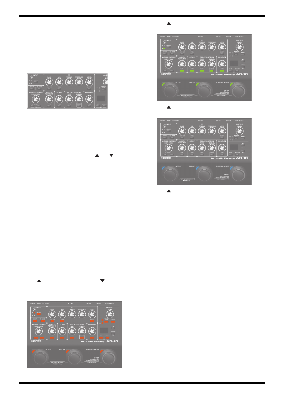
Press when the XLR LED flashes and press when the LINE
LED flashes.
When buttons until TUNER & MUTE have been pressed, the LEDs shown
in the figure light up red.
fig.led-red.eps
2. Press .
The LEDs shown in the figure light up green.
fig.led-green.eps
3. Press .
The LEDs shown in the figure light up blue.
fig.led-blue.eps
4. Press .
Each segment of the 7-segment LED display lights up in sequence and
when all segments light up, then they go dark in sequence.
Thereafter, this is repeated.
5. Hold down EXIT and press MEMORY, and then follow the procedure of
Executing or Skipping Test Items (p. 15) to advance to the next test
item.
5. Volume Check
This verifies the operations of volumes.
The INPUT CH1 LED flashes and 0_ appears on the 7-segment LED
display.
1. Turn slowly the INPUT SENS knob at the leftmost of the rear panel
clockwise; see from rear side.
At the center position, the center segment on the right digit of the 7segment LED display lights up.
2. Furthermore turn it clockwise to maximum.
The INPUT CH1 LED goes dark, the INPUT CH2 LED flashes and 1_
appears on the 7-segment LED display.
3. In the same way as steps 1 and 2, turn slowly the right INPUT SENS
knob and verify that the lower segment on the right digit of the 7-segment
LED display lights up, and then the center segment lights up.
4. In the same way, verify the knobs corresponding to the flashing buttons
in sequence.
*Turn EQ TREBLE when BOOST flashes and turn EQ PRESENSE when FX
LOOP flashes.
When all volumes are verified, ok appears on the 7-segment LED
display.
5. Hold down EXIT and press MEMORY, and then follow the procedure of
Executing or Skipping Test Items (p. 15) to advance to the next test
item.
16
Page 17
AD-10Sep. 2017
Sh Expression Pedal Check
* Before the unit enters this test item, connect the expression pedal to the CTL
1,2/EXP jack.
This verifies the operation of the expression pedal.
1. Connect the expression pedal to the CTL 1,2/EXP jack.
2. Completely depress the toe and heel of the pedal and verify that the
display on the 7-segment LED display changes from 00 to 7F.
3. Detach the expression pedal.
4. Hold down EXIT and press MEMORY, and then follow the procedure of
Executing or Skipping Test Items (p. 15) to advance to the next test
item.
SA Audio Check
1. Set the STEREO/MONO switch to MONO.
2. Connect the oscillator to the GUITAR IN 1 jack and input a signal like the
following.
GUITAR IN 1: 200-Hz sine wave at 5 Vpp
3. Connect the oscilloscope between HOT and GND and between COLD
and GND of the XLR OUT L connector.
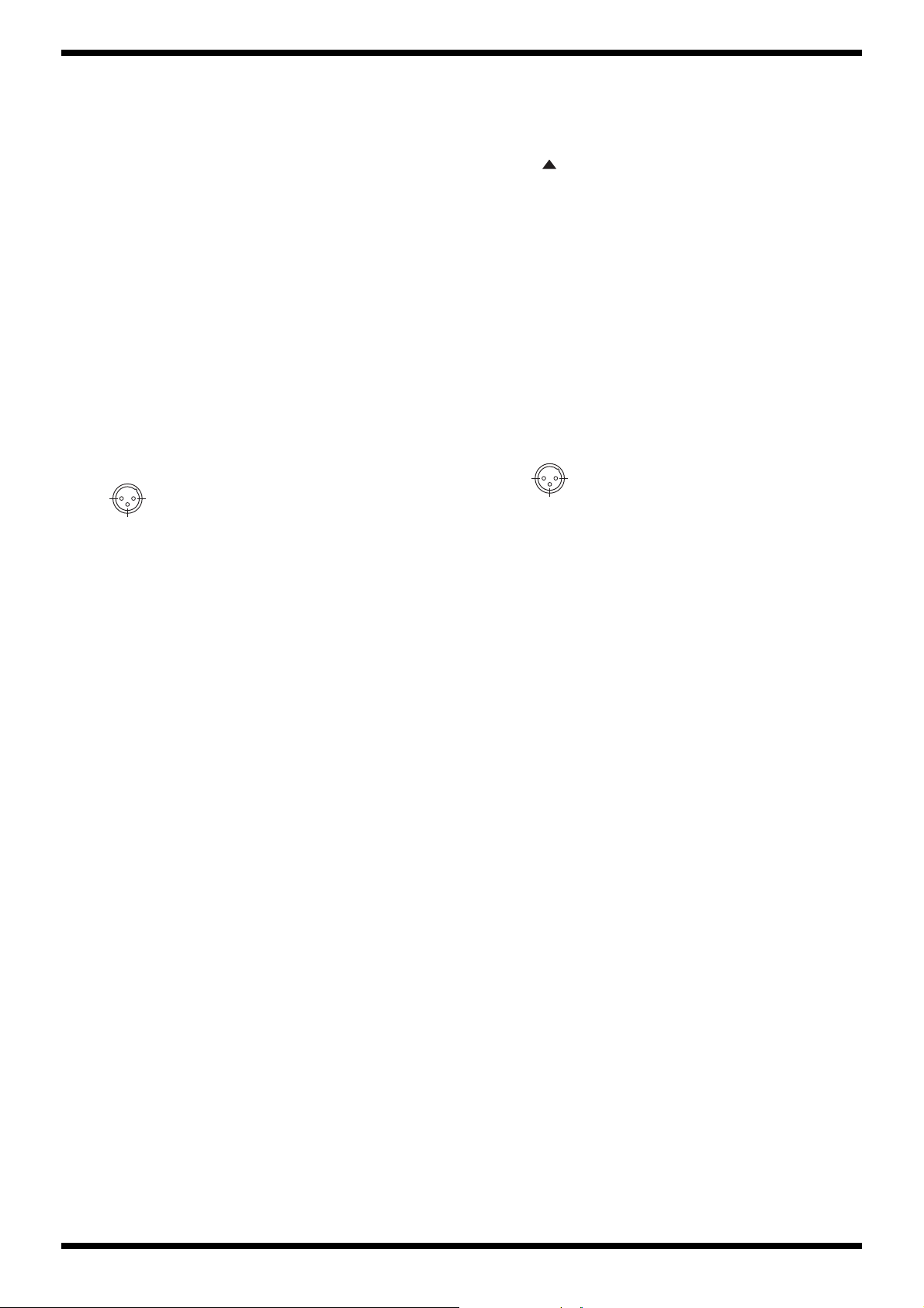
fig.XLR-male.eps
2: HOT1: GND
3: COLD
4. Verify that signals like the following are output from the XLR OUT L
connector.
XLR OUT L (HOT): 200-Hz sine wave at 5±0.3 Vpp
XLR OUT L (COLD): 200-Hz sine wave at 5±0.3 Vpp (reverse phase)
5. Connect the oscilloscope between HOT and GND and between COLD
and GND of the XLR OUT R connector, and verify that signals like the
following are output.
XLR OUT R (HOT): 200-Hz sine wave at 5±0.3 Vpp
XLR OUT R (COLD): 200-Hz sine wave at 5±0.3 Vpp (reverse phase)
6. Connect the oscillator to the GUITAR IN 2 jack and input a signal like the
following.
GUITAR IN 2: 200-Hz sine wave at 5 Vpp
7. Connect the oscilloscope to the LINE OUT L/PHONES and R/MONO
jacks.
* When the oscilloscope is connected to only one jack, connect a dummy plug to
another jack.
* Connect the oscilloscope between Tip and GND of each jack.
8. Verify that signals like the following are output from the LINE OUT L/
PHONES and R/MONO jacks.
LINE OUT L: 200-Hz sine wave at 5±0.3 Vpp
LINE OUT R: 200-Hz sine wave at 5±0.3 Vpp
9. Connect the oscilloscope to the LINE OUT L/PHONES jack.
* Connect it between Tip and Sleeve, and between Ring and Sleeve.
* Connect nothing to the LINE OUT R/MONO jack.
10. Verify that signals like the following are output from the LINE OUT L/
PHONES jacks.
LINE OUT L (Tip): 200-Hz sine wave at 5±0.3 Vpp
LINE OUT L (Ring): 200-Hz sine wave at 5±0.3 Vpp
11. Connect the oscillator to the RETURN jack and input a signal like the
following.
RETURN: 200-Hz sine wave at 5 Vpp
12. Connect the oscilloscope to the SEND jack and verify that a signal like the
following is output.
SEND: 200-Hz sine wave at 5±0.3 Vpp
SA Noise check
1. Verify that the STEREO/MONO switch is set at MONO.
2. Set the both INPUT SENS knobs and all knobs on the top cover to the
minimum.
3. Press three times to display 40 on the 7-segment LED display.
4. Connect the 1/4-inch monaural phone plugs with 47-kΩ load resistors to
the GUITAR IN 1, GUITAR IN 2 and RETURN jacks.
5. Verify that the residual noises at respective jacks are as follows.
XLR OUT L (HOT-GND): -60 dBm or less (DIN-Audio)
XLR OUT L (COLD-GND): -60 dBm or less (DIN-Audio)
XLR OUT R (HOT-GND): -60 dBm or less (DIN-Audio)
XLR OUT R (COLD-GND): -60 dBm or less (DIN-Audio)
LINE OUT L: -60 dBm or less (DIN-Audio)
LINE OUT R: -60 dBm or less (DIN-Audio)
SEND: -60 dBm or less (DIN-Audio)
GND LIFT Check
1. Set the GND switch on the rear panel to NOR.
2. Using a tester, verify that GND of the XLR OUT L connector and GND of
the LINE OUT L/PHONES (or R/MONO) jacks have continuity.
fig.XLR-male.eps
2: HOT1: GND
3: COLD
3. Verify that GND of the XLR OUT R connector and GND of the LINE OUT
L/PHONES (or R/MONO) jacks have continuity.
4. Set the GND switch to LIFT.
5. Verify that GND of the XLR OUT L connector and GND of the LINE OUT
L/PHONES (or R/MONO) jacks do not have continuity.
6. Verify that GND of the XLR OUT R connector and GND of the LINE OUT
L/PHONES (or R/MONO) jacks do not have continuity.
17
Page 18
Sep. 2017 AD-10
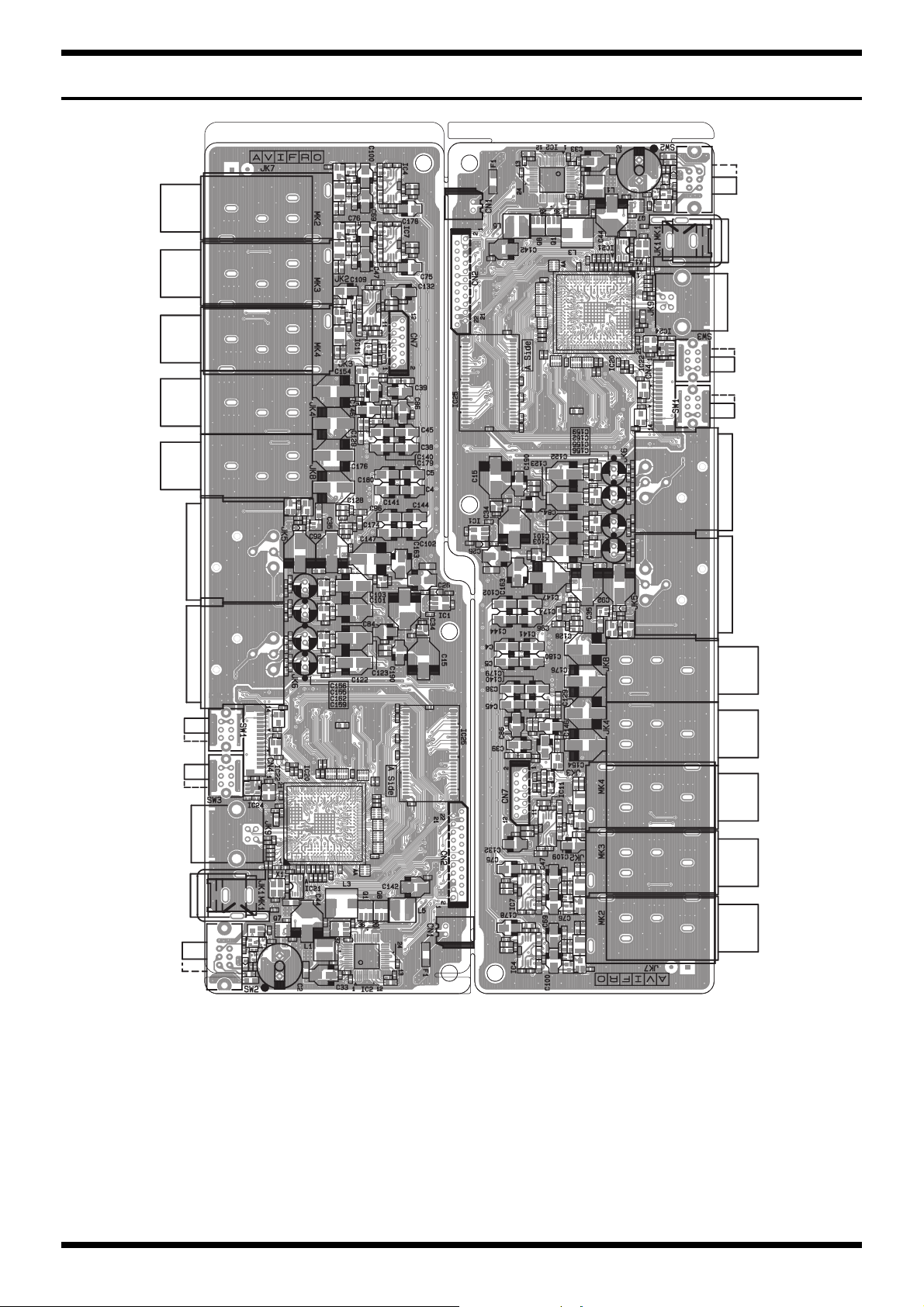
Circuit Board (Main Board)
fig.b-main-1.eps
18
Page 19
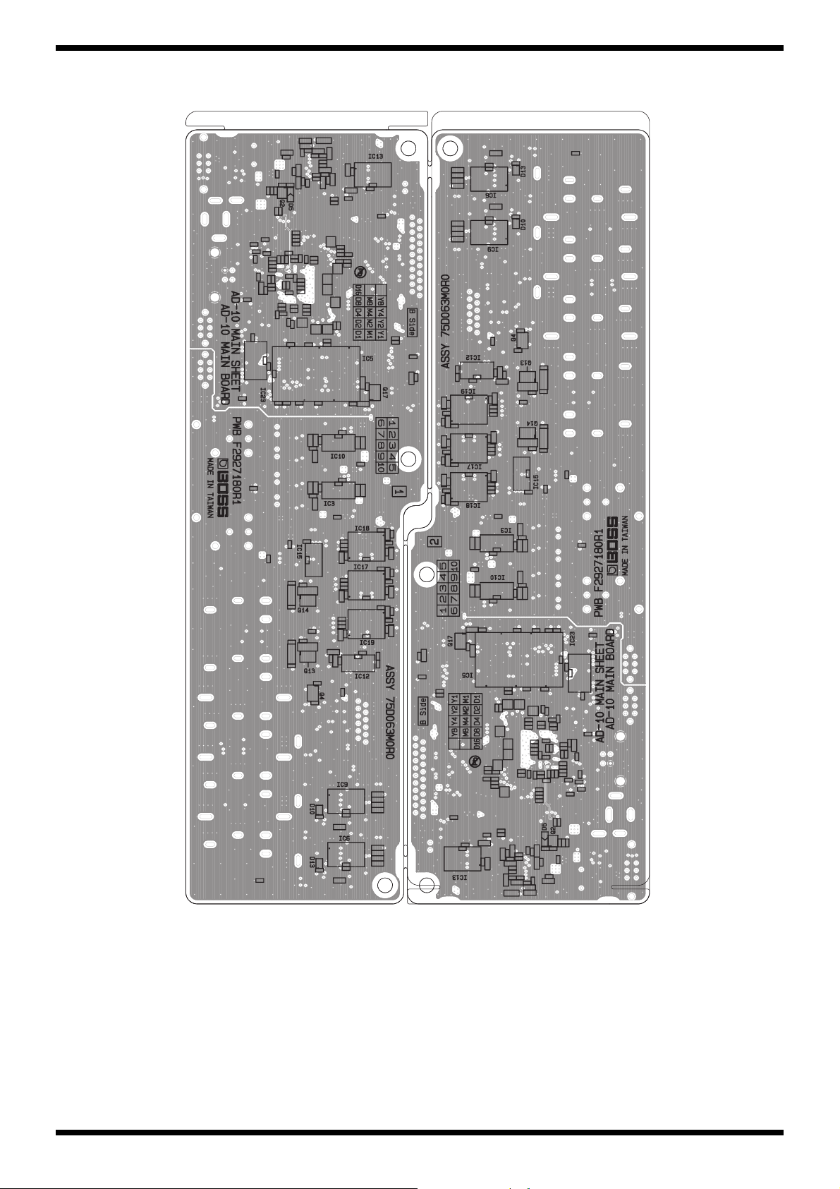
fig.b-main-2.eps
AD-10Sep. 2017
19
Page 20
Sep. 2017 AD-10
GND
GND
GND
GND
FB+1.2
FB+1.
FBD+3.3
GND
AVCC
GND
AVCC-PHONE
GND
FBA+4
GND
PVCC
GND
D+3.3
GND GND
D+1.2AVCC
GND
XSWD-PWR
XOFF-PWR
FBD+3
GND
GNDGND
GND
GNDGND
GND
D+3.3
GND
GND
PVCC
GND
PVCC
FBA+4
GND
GND
0.1uF
C7
0.1uF
C43
0.1uF
C11
100pF
C29
0.1uF
C55
IC2
MB39A123PMT-G-JN-EFE1
-INE1
38
FB1
37
CS1
39
-INE2
41
FB2
42
CS2
40
DTC2
43
-INE3
46
FB3
45
CS3
47
DTC3
44
-INA
19
OUTA
18
-INE4
16
FB4
15
CS4
17
DTC4
14
-INE5
21
FB5
22
CS5
20
DTC5
23
-INE6
26
FB6
25
CS6
27
DTC6
24
VREF
9
-INS
8
CSCP
13
CTL1
2
CTL2
3
CTL3
4
CTL4
5
CTL5
6
CTL6
7
CTL
1
GND
10
GNDO
28
CT
12
RT
11
OUT6
29
OUT5
30
OUT4
31
OUT3
32
OUT2
33
OUT1-2
34
OUT1-1
35
VCCO
36
VCC
48
QS5U27TR(PB FREE)
Q1
34
Q8
QS5U27TR(PB FREE)
34
Q8
QS5U27TR(PB FREE)
1
52
Q1
QS5U27TR(PB FREE)
1
5
2
6.8k
R5
0.5%
0
R9
10k
R8
TP10 TP13
1uF
C8
0.1uF
C32
0.1uF
C3
QS8J4TR
Q7
2
187
0.1uF
C14
QS8J4TR
Q7
4
365
33k
R36
ERBRG1R00V
F1
0.1uF
C71
330k
R38
330k
R37
TP76
TP77
C2
1000uF
16V
0.1uF
C17
Q3
QS5U27TR(PB FREE)
34
0.1uF
C9
Q3
QS5U27TR(PB FREE)
1
5
2
TP81
TP79
33k
R307
0.5%
TP78
TP83TP82
TP84
2SC4738-GR(TE85L.F)
Q5
1
23
C21
0.1uF
R10
2.2k
2SC4738-GR(TE85L.F)
Q6
1
23
TP7
C148
0.1uF
R24
2.2k
C142
10uF
16V
C15
100uF
16V
C34
16V
100uF
16V
10uF
C12
2012
1500pF
C10
3.9k
R40
0.5%
560
R339
0.5%
22k
R20
0.5%
3.9k
R13
22k
R310
0.5%
33k
R302
0.5%
2200pF
C40
TP11
33k
R43
0.5%
0.01uF
C28
0.015uF
C27
0.015uF
C13
22uH
VLCF4024T-220MR65-2
L1
12
0.1uF
C51
TP111
TP112
TP116
TP121
TP122
TP123
TP125
FS-7 DC JACK HOLDER
MK1
10
FS-7 DC JACK HOLDER
MK1
20
TP176
Q2
2SA1832-GR
2
3
1
22k
R3
0.01uF
C18
100uH
VLCF5028T-101MR33-2
L5
12
27k
R12
0.5%
27k
R27
0.5%
2200pF
C19
27k
R44
0.033uF
C36
TP86
SV71010F-0202-6T-NP
SW2
11
1312
SV71010F-0202-6T-NP
SW2
21
2322
SV71010F-0202-6T-NP
SW2
10
SV71010F-0202-6T-NP
SW2
20
22k
R34
15k
R35
KM02020ABM2P
JK1
3
1
2
TP5
TP6
53015-0210
CN1
1
53015-0210
CN1
2
100uH
CLF6045NIT-101M
L3
12
C147
220uF
16V
C163
22uF
16V
C340
0.1uF
C341
0.1uF
C342
0.1uF
C343
0.1uF
C344
0.1uF
C345
0.1uF
C346
0.1uF
C347
0.1uF
C348
0.1uF
C349
0.1uF
C350
0.1uF
C351
0.1uF
C352
0.1uF
C357
0.1uF
0
R26
1608
0.022uF
C37
DTC114EUAT106(PB FREE)
Q47
1
2
3
1SS361FV
D4
3
21
16V
10uF
C58
D6
1SS387
10k
R100
D11 UnPop
2
3
1
R143
1k
TP115
TP124 TP190
100
R118
1608
Q46
2SA1832-GR
23
1
47k
R42
TP12
100k
R39
TP85
R77
UnPop
UDZV TE-17 10B
D5
0.47uF
C1
50V
18k
R303
15k
R17
TP4
TP46
TP59
TP74
C57
0.1uF
25V
Fosc=1.00MHz
+3.96V
DC IN
(PSA-**S)
8.55 - 9.5V
+
5.4-9.0V
BAT IN
(AA x 6)
+1.2V
+3.28V
11.2V
11.8V
POWER ON
SW2 12
11 / 22 21
AD-10 MAIN BOARD (Power)
POWER SW
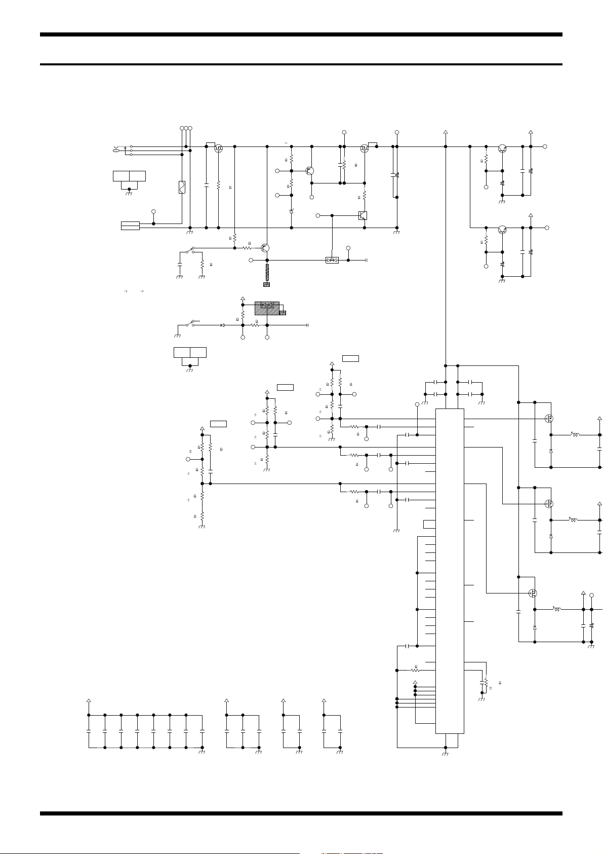
Circuit Diagram (Main Board: 1/3)
fig.d-main-1.eps@L
20
Page 21
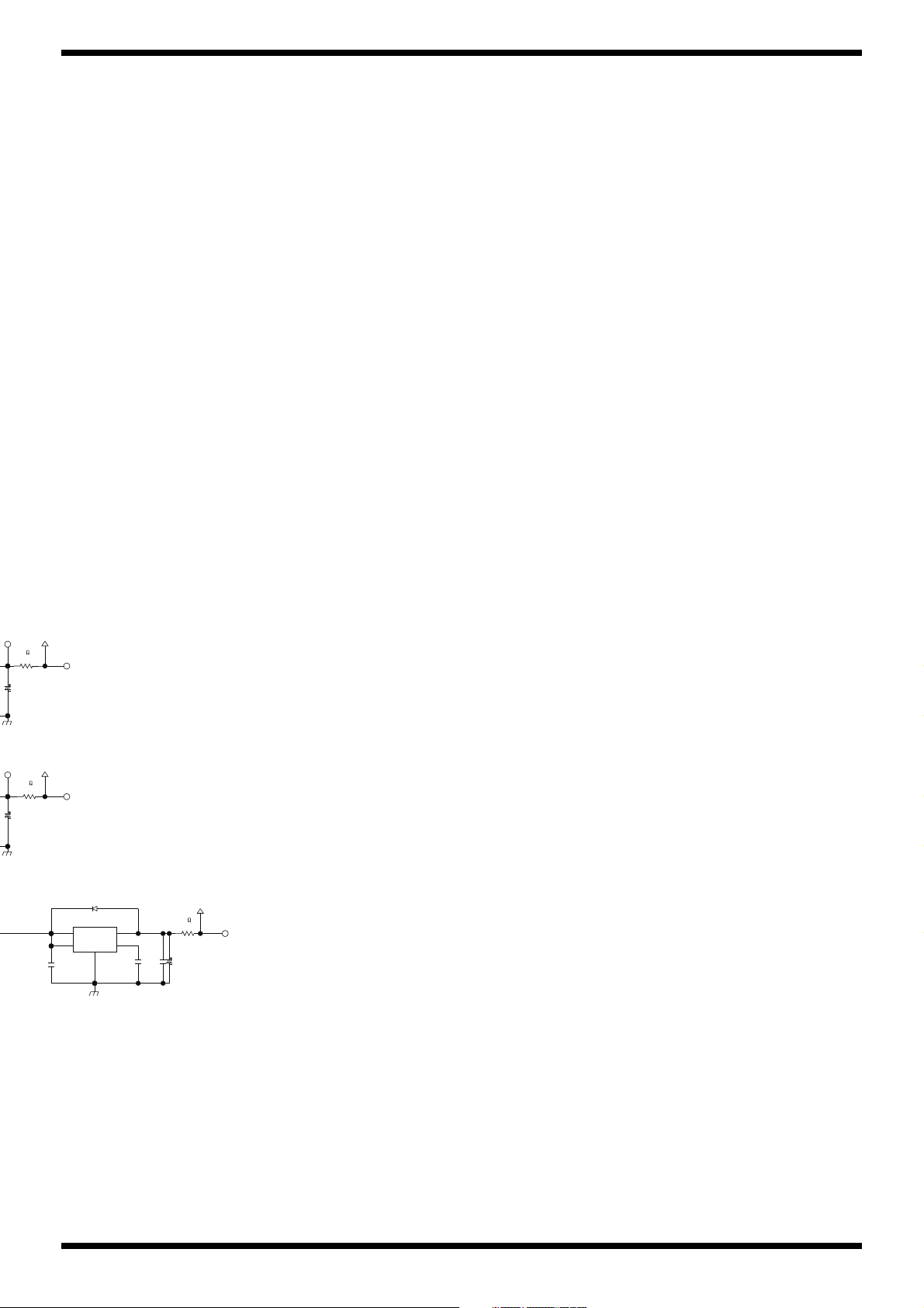
fig.d-main-1.eps@R
D+3.3
2
GND
A+3.3
.3
D+1.2
GND
GND
0
R16
2012
0
R18
2012
TP110
C338
0.1uF
C33
47uF
6.3V
C44
100uF
16V
C26
10uF
16V
TP9
TP80
TP2
TP3
NJM2882F33-TE1
IC1
1
VIN
3
CTRL
2
GND
4
N-BP
5
VOUT
C6
0.1uF0.01uF
C31
0
R4
2012
D1
1SS387
AD-10Sep. 2017
21
Page 22
Sep. 2017 AD-10
SDAD1
SDDA1
A+3.3
SDAD0
D+3.3
A+3.3
GND
SDDA2
GND
GND
GND
GND
GND
AVCC
GND
GND
GND
MCK0
BCK0
LRCK0
BCK0
LRCK0
MCK0
BCK0
LRCK0
MCK0
XCODEC-PDN
XCODEC-PDN
XCODEC-PDN
GNDGND
SDAD2
A+3.3
AVCC
GND
GND
GND
GND
GTR1-DET
ADREF-GTR1
ADREF-GTR1
ADREF-GTR1
GND
ADREF-GTR2
GND
GND
A+3.3
D+3.3
GND
GND
AVCC
ADREF-GTR2
GTR2-DET
GND
AVCC
GND
GND
GND
GND
A+3.3
ADREF-RTN
ADREF-RTN
D+3.3
AVCC
GND
GND
GND
GND
GND
ADREF-RTN
RTN-DET
GND
GND
GND
GND
GND
A+3.3
SDDA0
A+3.3
GND
GND
ADREF-GTR2
A+3.3
AVCC
GND
GND
DAREF-XLR
DAREF-OUT
AVCC-PHONE
MPX2-A
MPX2-B
MPX1-A
MPX1-B
AVREF-SR
GND
GND
AVCC
GND
GND
GND
GND
GND
0.1uF
C172
0.1uF
C181
0.1uF
C183
TP39
DTA114EUAT106 (PB FREE)
Q17
1
32
0.1uF
C171
0.1uF
C112
0.1uF
C118
0.1uF
C113
0.1uF
C120
0.1uF
C175
0.1uF
C182
0.1uF
C177
0.1uFC110
0.1uF
C173
0.1uF
C106
IC4
NJM2115V(TE1)
3
1
2
IC4
NJM2115V(TE1)
5
7
6
NJM2115V(TE1)
IC4
48
NJM4580V-TE1-#Z#ZB
IC3
48
NJM4580V-TE1-#Z#ZB
IC10
48
1SS362FV
D13 2
3
1
0.1uF
C88
10k
R158
0.5%
R154
0.5%
470
2SK880-GR
Q26
3
1
2
R157
33k
10k
R75
0.5%
100
R69
100
R151
C187
1uF
3225
100
R146
TP53
TP54
TP21
TP20
150k
R61
0.5%
TP25
TP48
TP41
10M
R15
1608
C69
10uF
16V
C100
10uF
16V
C102
10uF
16V
C144
10uF
16V
0.1uF
C165
10k
R109
0.5%
0.1uF
C94C178
10uF
16V
10k
R92
0.5%
10k
R58
0.5%
C179
10uF
16V
C140
10uF
16V
C180
10uF
16V
C141
10uF
16V
C174
10uF
16V
C96
10uF
16V
C190
10uF
16V
2SC4738-GR
Q27
1
2
3
TP135
C54
UnPop
0
R80
0
R148
0R160
0
R173
0
R172
0
R162
0
R306
0
R305
0
R177
TP168
TP137
TP132
MK2
GT-10 JACK COVER L
10
20
30
C80
UnPop
C82
UnPop
C117 UnPop
10k
R159
0.5%
TP178TP179
TP187
10k
R155
1608
C188
UnPop
6.3V
10uF
C61
6.3V
10uF
C62
6.3V
10uF
C63
6.3V
10uF
C64
6.3V
10uF
C65
6.3V
10uF
C66
HTJ-064-22HSPP
JK7
1
3
4
2
1SS362FV
D12
2
3
1
22pF
C81
AK4556VT-E2
IC18
2
LIN
1
RIN
13
SDTI
14
LRCK
15
MCLK
16
BCLK
7
DEM1
6
DEM0
17
PDN
12
CKS3
11
CKS2
10
CKS1
9
CKS0
3
VSS
18
VCOM
8
SDTO
20
ROUT
19
LOUT
5
VD
4
VA
AK4556VT-E2
IC19
2
LIN
1
RIN
13
SDTI
14
LRCK
15
MCLK
16
BCLK
7
DEM1
6
DEM0
17
PDN
12
CKS3
11
CKS2
10
CKS1
9
CKS0
3
VSS
18
VCOM
8
SDTO
20
ROUT
19
LOUT
5
VD
4
VA
AK4556VT-E2
IC17
2
LIN
1
RIN
13
SDTI
14
LRCK
15
MCLK
16
BCLK
7
DEM1
6
DEM0
17
PDN
12
CKS3
11
CKS2
10
CKS1
9
CKS0
3
VSS
18
VCOM
8
SDTO
20
ROUT
19
LOUT
5
VD
4
VA
C4
10uF
16V
C5
10uF
16V
C38
10uF
16V
C45
10uF
16V
C90
UnPop
0.1uF
C79
HTJ-064-22HSPP
JK2
1
3
4
2
150k
R11
0.5%
4.7k
R60
TP8
TP14
TP27
TP19
10k
R31
0.5%
R90
33k
1SS362FV
D8
2
3
1
IC7
NJM2115V(TE1)
5
7
6
IC7
NJM2115V(TE1)
3
1
2
22pF
C70
C89
1uF
3225
C76
10uF
16V
2SK880-GR
Q28
3
1
2
C47
10uF
16V
10M
R1
1608
R67
0.5%
470
10k
R95
0.5%
TP60
TP36
C46
UnPop
1SS362FV
D10 2
3
1
2SC4738-GR
Q29
1
23
10k
R96
0.5%
MK3
GT-10 JACK COVER L
10
20
30
C60
UnPop
C72
UnPop
DTA114EUAT106 (PB FREE)
Q15
1
32
TP68TP71
C78 UnPop
10k
R88
1608
C93
UnPop
TP139
MK4
GT-10 JACK COVER L
UnPop
10
20
30
C99
UnPop
C105
UnPop
DTA114EUAT106 (PB FREE)
Q31
1
32
C116 UnPop
10k
R142
1608
C134
UnPop
HTJ-064-22HSPP
JK3
1
3
4
2
150k
R103
0.5%
4.7k
R132
TP87
TP88
TP136
10k
R112
0.5%
10k
R110
0.5%
NJM2115V(TE1)
IC11
48
C132
10uF
16V
0.1uF
C108
1SS362FV
D15
2
3
1
IC11
NJM2115V(TE1)
5
7
6
10k
R126
0.5%
IC11
NJM2115V(TE1)
3
1
2
22pF
C104
C133
1uF
3225
C109
10uF
16V
2SK880-GR
Q33
3
12
0.1uF
C107
TP138
NJM2115V(TE1)
IC7
48
10k
R53
0.5%
0.1uF
C73C75
10uF
16V
10k
R33
0.5%
TP24
0.1uF
C20
NJM3414AV-TE1
IC15
4
V-
8
V+
NJM4580V-TE1-#Z#ZB
IC12
4
V-
8
V+
TP34
10k
R166
0.5%
0.1uF
C87
12k
R167
0.5%
C84
10uF
16V
220k
R98
R106
0.5%10k
12k
R65
0.5%
R84
0.5%
10k
4.7
R147
4.7
R152
4.7
R116
6.3V
10uF
C52
6.3V
10uF
C68
6.3V
10uF
C67
R49
0.5%10k
27k
R74
0.5%
27k
R28
0.5%
27k
R107
0.5%
5.6k
R72
0.5%
5.6k
R21
0.5%
5.6k
R105
0.5%
33k
R94 0.5%
33k
R45 0.5%
100k
R14 0.5%
100k
R83 0.5%
3300pF
C77
3300pF
C115
3300pF
C111
TP75
TP113
TP114
TP117
TP118
TP119
TP120
TP130
TP133
270k
R7 0.5%
270k
R82 0.5%
SN74LV4052APWR
IC6
9
B
10
A
2
2Y
14
1X
2X
15
16
VCC
3
YCOM
7
VEE
1Y
5
3Y
4
INH
6
1
0Y
XCOM
13
11
3X
0X
12
GND
8
SN74LV4052APWR
IC9
9
B
10
A
2
2Y
14
1X
2X
15
16
VCC
3
YCOM
7
VEE
1Y
5
3Y
4
INH
6
1
0Y
XCOM
13
11
3X
0X
12
GND
8
10k
R161
0.5%
C35
100uF
16V
33k
R32
0.5%
33k
R66
0.5%
2.7k
R117
D/A Full +0.46dBu
A/D Full +0.46dBu
GTR 1
AD-10 MAIN BOARD (Analog)
Film
Film
+23.52dB
GTR 2
Film
+23.52dB
RETURN
D/A Full +0.46dBu
A/D Full +0.46dBu
D/A Full +0.46dBu
A/D Full +0.46dBu
typ:-10dBu
max:+7dBu
typ:-10dBu
max:+7dBu
typ:-10dBu
max:+7dBu
+23.52dB
fc1=1.48kHz
fc2=8.61kHz
Gain=15.3dB
gain0=-8.55dB
gain1=+1.76dB
gain2=+11.38dB
gain3=+20.00dB
-8.63dB
fc1=1.48kHz
fc2=8.61kHz
Gain=15.3dB
gain0=-8.55dB
gain1=+1.76dB
gain2=+11.38dB
gain3=+20.00dB
Circuit Diagram (Main Board: 2/3)
fig.d-main-2.eps@L
22
Page 23
DAREF-XLR
DAREF-XLR
DAREF-XLR
DAREF-XLR
GND
GND
GND
GND
GND
GND
DAREF-OUT
DAREF-OUT
GND
GND
GND
GND
PVCC
GND
XCPU_MUTE
GND
GND
GND
SEND
GNDGND
GND
OUTR-DET
GND
D+3.3
ST-MONO
GND
GND
GND
GND
GND
AVREF-SR
AVREF-SR
47pF
C157
100k
R62
47pF
C150
TP38
TP22
TP15
TP28
TP40
TP43
TP57
DTC614TU T106
Q19
1
23
DTC614TU T106
Q13
1
2
3
DTC614TU T106
Q21
1
23
SW1
SV69010F-0202-6V-NP-001
10
20
DTC614TU T106
Q23
1
23
SW1
SV69010F-0202-6V-NP-001
11
13 12
DTC614TU T106
Q14
1
23
21
23 22
IC10
NJM4580V-TE1-#Z#ZB
3
1
2
IC3
NJM4580V-TE1-#Z#ZB
3
1
2
IC3
NJM4580V-TE1-#Z#ZB
5
7
6
IC10
NJM4580V-TE1-#Z#ZB
5
7
6
4.7k
R130
0.5%
C155
22uF
63V
C156
22uF
63V
TP26
TP33
TP18
TP32
4.7k
R81
0.5%
4.7k
R138
0.5%
TP23
4.7k
R89
0.5%
TP35
100k
R134
47pF
C143
47pF
C130
TP31
47pF
C131
TP29
0.1uF
C169
C153
UnPop
150
R3010R325
0
R326
150
R327
0
R63
0
R93
100k
R145
DTC614TU T106
Q22
1
23
TP47
150
R334
150
R335
DTC614TU T106
Q25
1
23
C159
22uF
63V
100k
R120
TP58
C162
22uF
63V
C166
UnPop
C164
UnPop
TP50TP37
100k
R73
100k
R125
100k
R340
100k
R341
100k
R309
100k
R342
TP126
TP127
TP128
TP129
TP131
C86
10uF
16V
TP148
TP151
TP159
TP163
TP164
TP165
C114
UnPop
C119
UnPop
10k
R55
100k
R87
10k
R78
D9
1SS387(TPH3.F)
Q24
2SA1832-GR
23
1
TP55
TP51
DTC114TUAT106
Q10
1
23
10k
R85
DTC114TUAT106
Q11
1
23
TP56
TP89
TP90
TP91
TP92
150
R299
1608
150
R328
1608
150
R332
1608
150
R336
1608
16V
10uF
C59
TP150
HTJ-064-22HSPP
JK4
1
3
4
2
HTJ-064-22HSPP
JK8
1
3
4
2
C50
10uF
16V
330
R179
C146
10uF
16V
680
R128
1608
100k
R123
22
R178
1/4W
3216
22
R86
1/4W
3216
22
R91
1/4W
3216
22
R163
1/4W
3216
C128
220uF
16V
C129
220uF
16V
C176
220uF
16V
C154
220uF
16V
1k
R70
1k
R64
SW3
SV69010F-0202-6V-NP-001
10
20
SW3
SV69010F-0202-6V-NP-001
11
1312
21
2322
DTA114EUAT106 (PB FREE)
Q4
1
3
2
TP1
4.7k
R124
C16
UnPop
IC15
NJM3414AV-TE1
5
7
6
IC15
NJM3414AV-TE1
3
1
2
IC12
NJM4580V-TE1-#Z#ZB
3
1
2
IC12
NJM4580V-TE1-#Z#ZB
5
7
6
10k
R99
0.5%
10k
R102
0.5%
10k
R164
0.5%
10k
R165
0.5%
4700pF
C138
4700pF
C137
C92
220uF
16V
10k
R51
0.5%
10k
R56
0.5%
10k
R47
0.5%
10k
R48
0.5%
27k
R122
0.5%
27k
R104
0.5%
27k
R79
0.5%
27k
R71
0.5%
27k
R41
0.5%
27k
R168
0.5%
5.6k
R22
0.5%
5.6k
R19
0.5%
5.6k
R101
0.5%
5.6k
R25
0.5%
5.6k
R23
0.5%
3300pF
C23
3300pF
C22
3300pF
C24
3300pF
C25
3300pF
C30
3300pF
C41
C122
47uF
16V
C123
47uF
16V
C101
47uF
16V
C103
47uF
16V
TP140
TP142
TP143
TP145
TP146
TP147
TP152
TP153
TP154
TP155
TP156
5.6k
R113
0.5%
C39
10uF
16V
JK5
CT3-05M-EP
10
1
3
2
JK6
CT3-05M-EP
10
1
3
2
47pF
C48
10
R59
[GND LIFT]
XLR OUT R
XLR OUT L
OUTPUT R
(MONO)
Mute ON: L
GND LIFT
SW1:22
23 / 12 13
HOT
COLD
HOT
COLD
OUTPUT L
(PHONES)
[STEREO/MONO]
typ:-10dBu
max:+7dBu
typ:-10dBu
max:+7dBu
typ:-10dBu
max:+7dBu
typ:-10dBu
max:+7dBu
typ:-10dBu
max:+7dBu
12-11/22-21=L:STEREO
12-13/22-23=H:MONO
gain=+8.63dB
fc1=1.48kHz
fc2=8.61kHz
Gain=15.3dB
gain=+8.63dB
fc1=1.48kHz
fc2=8.61kHz
Gain=15.3dB
gain=+8.63dB
fc1=1.48kHz
fc2=8.61kHz
Gain=15.3dB
gain=+8.63dB
fc1=1.48kHz
fc2=8.61kHz
Gain=15.3dB
gain=+8.63dB
fc1=1.48kHz
fc2=8.61kHz
Gain=15.3dB
fig.d-main-2.eps@R
AD-10Sep. 2017
23
Page 24
Sep. 2017 AD-10
GND
GND
XMWE-M
GND
D+3.3
GND
D+1.2
MDQM1-M
XMWR-CAS-M
MCKO-M
GND
GND
D+3.3
D+3.3
D+3.3
D+3.3
D+3.3
XSF-WP
XMSDRCS-M
CKUDL-M
XMRD-RAS-M
D+3.3
GND
D+1.2
GND
MDQM0-M
MCKE-M
CKCPU-M
D+3.3
GND
GND
D+3.3
GND
XICE-RESET
MPX1-A
MPX1-B
XSFICS
SFIDI
SFIDO
SFICK
XSFIHLD
GND
D+1.2
SDDA2
SDDA1
SDDA0
SDAD2
SDAD1
SDAD0
BCK0
MCK0
GND
XSWD-PWR
XOFF-PWR
GND
GND
LRCK0
D+3.3
TIP
RING
MPXM-X
MPXM-X
MPXM-Y
MPXM-Y
MPXP2-X
MPXP2-X
MPXP2-Y
MPXP2-Y
MPXP1-X
MPXP1-X
MPXP1-Y
MPXP1-Y
MPX2-B
MPX2-A
ADMPX-A
ADMPX-A
ADMPX-B
ADMPX-B
ADMPX-A
ADMPX-B
D+3.3
GND
LEDD1
LEDD0
LED-SCK
LEDD2
LEDXG
LED-RCK
INPUT-SW
INPUT-SW
NOTCH-SW
NOTCH-SW
LEDD3
EQ-SW
EQ-SW
GND
D+3.3
D+3.3
SENS2
SENS2
SENS1
SENS1
PVCC
D+3.3
GND
EXIT
MEMORY
ST-MONO
GND
D+3.3
RTN-DET
GTR2-DET
CTL-DET
CTL-DET
XICE-RESET
SEND
GND
D+3.3
CTL-RING
CTL-TIP
0
R253
0
R200
0
R201
0
R202
0
R204
0
R205
0
R206
0
R208
0.01uF
C248
0.01uF
C245
0.01uFC246
0.01uF
C247
0.01uF
C249
0.01uFC250
0.01uFC251
0.01uFC252
0.1uF
C223
150
R198
150
R221
150
R222
100
R192
150
RA15
18
6543
27
100
R193
150
R223
100
R194
100
R196
R207
UnPop
100
R219
10k
R214
100
R220
TP67
TP69
TP70
BD45301G-TR
IC24
5
VDD
3
GND
2
SUB
1
ER
4
VOUT
TP72
1uF
C193
1uF
C202
56k
R230
100
R243
100
R244
100
R249
C236
0.1uF
100
R252
100
R293
IC20
N2
N1
N4
R4
R3
T2
P2
D3
D2
C1
E2
E3
E1
H4
H3
J4
J3
G2
G1
H2
H1
J2
J1
K2
K1
L3
L2
L1
L4
M2
M1
N3
R2
R1
TC7WU04FU
IC21
17
0
R199
TC7WU04FU
IC21
62
10k
R211
TC7WU04FU
IC21
48
0.1uF
C220
TC7WU04FU
IC21
35
C215
UnPop
0.1uF
C222
IC20
MB8AA4181
F2
C2
B1
Y1
B2
A2
C16
C12
D16
C4
B6
D5
A6
C7
A3
B4
C5
D6
K21
K20
H20
J20
V21
Y16
AA17
Y20
W17
Y18
Y17
AA16
W18
F3
A4
B5
C6
A5
F21
F20
E21
E20
H21
D8
C8
AA2
AA20
Y21
A17
C20
D20
E19
F19
G20
B19
C21
B20
A20
B21
C18
B18
A19
B3
DSX321G 16.9344MHZ
X1
1
2
4
3
680
R218
1M
R210
10k
R216
DSO321SR 48.000MHZ 50PPM
IC22
VDD
4
GND2OUT
3
OE
1
47
R231
1uF
C203
CN4
UnPop
0.1uF
C225
270
R236
1uF
C205
1uF
C331
10k
R311
0.5%
100
R321
100
R322
100
R29
100
R30
100
R52
100
R76
33k
R312
0.5%
TP93
TP94
TP95
TP96
TP97
TP98
TP99
TP102
TP103
TP104
TP105
TP106
TP107
TP108
TP109
TP177
10pF
C255
10pF
C256
1k
R156
100
R150
0
R46 0
R57
1SS362FV
D7
2
3
1
470k
R182
1SS362FV
D14
2
3
1
CN7
12FMN-BTK-A (LF)(SN)
1
2
3
4
5
6
8
9
10
11
12
7
R183
4.7k
TP42
TP44
0.1uFC42
22FMN-BTK-A (LF)(SN)
CN2
1
2
3
4
5
6
7
8
9
10
11
12
13
14
15
16
17
18
19
20
21
22
100
R276
100
R274
100
R2
SN74LV4052APWR
IC13
9
B
10
A
2
2Y
14
1X
2X
15
16
VCC
3
YCOM
7
VEE
1Y
5
3Y
4
INH
6
1
0Y
XCOM
13
11
3X
0X
12
GND
8
0
R6
UnPop
56k
R278
56k
R279
10k
R54
MX25L1606EM2I-12G
IC23
6
SCLK
5
SI/SIO0
2
SO/SIO1
1
_CS
3
_WP
7
_HOLD
4
GND
8
VCC
R184 4.7k
1608
R185 4.7k
BMD0:BMD1:BMD:2
0:0:1
JTAG
(SFI BOOT)
"Serial Flash"
INTERNAL ROM BOOT
"BATTERY MONITOR"
AD-10 MAIN BOARD (Digital)
To PANEL BOARD CN2
To JACK BOARD CN201
Circuit Diagram (Main Board: 3/3)
fig.d-main-3.eps@L
24
Page 25
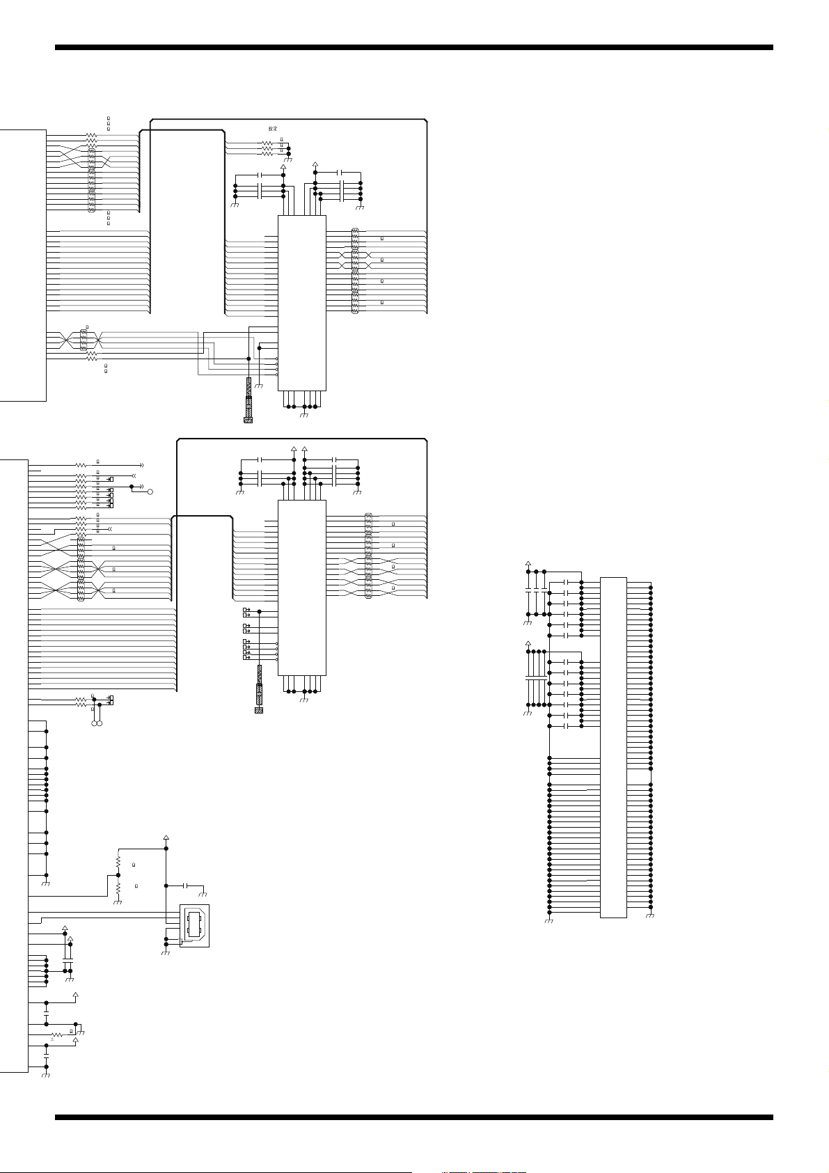
fig.d-main-3.eps@R
EA-M(13)
D+3.3
MA-M(3)
GND
MD-M(15:0)
GND
ED-M(5)
MD-M(7)
EA-M(6)
ED-M(0)
USB-D+
EA-M(12)
ED-M(15)
MD-M(8)
EA-M(10)
ED-M(6)
MD-M(10)
ED-M(7)
ED-M(13)
EA-M(14)
GND
MD-M(3)
EA-M(11)
XMSDRCS-M
MD-M(8)
EA-M(4)
MD-M(11)
GND
MA-M(6)
GND
MA-M(11:0),MA-M(15,14)
ED-M(13)
GND
ED-M(7)
ED-M(12)
XMRD-RAS-M
ED-M(0)
GND
MD-M(4)
MD-M(15)
MA-M(2)
MA-M(10)
D+3.3
MD-M(11)
MD-M(2)
MA-M(14)
D+3.3
D+3.3
ED-M(10)
ED-M(1)
D+3.3
ED-M(11)
GND
MCKO-M
EA-M(7)
MA-M(0)
MD-M(13)
ED-M(15)
MD-M(6)
GND
GND
GND
GND
EA-M(13)
ED-M(12)
D+1.2
EA-M(9)
EA-M(12)
MD-M(9)
EA-M(13)
EA-M(5)
EA-M(0)
EA-M(4)
ED-M(3)
MA-M(15)
EA-M(10)
ED-M(4)
GND
MA-M(10)
GND
ED-M(2)
EA-M(2)
MD-M(14)
MA-M(15)
EA-M(8)
MD-M(13)
EA-M(5)
EA-M(6)
MD-M(14)
GND
MD-M(1)
MD-M(1)
MD-M(9)
USB-D-
MA-M(8)
MD-M(12)
XMWE-M
EA-M(14)
ED-M(14)
EA-M(1)
MA-M(4)
MD-M(10)
ED-M(15:0)
GND
MD-M(0)
EA-M(2)
MD-M(12)
ED-M(4)
GND
D+1.2
ED-M(5)
ED-M(1)
MA-M(5)
MD-M(3)
D+3.3
MDQM0-M
MA-M(7)
ED-M(3)
MDQM1-M
D+3.3
EA-M(12)
ED-M(8)
MD-M(2)
ED-M(14)
ECKE-M
ECKE-M
MA-M(1)
MD-M(5)
EA-M(3)
EA-M(1)
ECKO-MECKO-M
ED-M(2)
ED-M(9)
MD-M(4)
MD-M(0)
EA-M(14:0)
MCKE-M
GND
MD-M(5)
EA-M(14)
MD-M(7)
MA-M(9)
MD-M(15)
MD-M(6)
ED-M(6)
XMWR-CAS-M
EA-M(7)
D+1.2
XCPU_MUTE
LEDD0
LEDD2
LEDD1
MA-M(14)
MA-M(11)
XCODEC-PDN
LED-RCK
LEDXG
GND
ED-M(9)
ED-M(8)
ED-M(10)
ED-M(11)
EA-M(3)
EA-M(0)
XECS-M
XECS-M
XERAS-MXERAS-M
XECAS-M
XECAS-M
XEWE-M
XEWE-M
EA-M(8)
EA-M(11)
EA-M(9)
MA-M(11)
MA-M(9)
MA-M(8)
MA-M(7)
MA-M(6)
MA-M(5)
MA-M(4)
MA-M(0)
MA-M(1)
MA-M(2)
MA-M(3)
GND
BUS+5
GND
LEDD3
LED-SCK
OUTR-DET
GTR1-DET
0.1uFC232
0.1uFC235
0.1uFC244
UBR24-4K5J00
JK9
3
2
1
4
10
20
0.1uFC240
0.1uFC213
0.1uFC224
0.1uFC226
0.1uFC230
0.1uFC234
0.1uFC238
1uFC197
1uFC194
1uF
C196
10uF
C243
1608
150
RA11
18
6543
27
150
R197
150
R234
150
RA9
18
6543
27
150
RA10
18
6543
27
150
RA12
18
6543
27
150
R188
150
R189
150
R229
150
RA4
18
6543
27
1uF
C195
10k
R212
150
RA1
18
6543
27
10k
R213
150
RA6
18
6543
27
10k
R215
150
RA7
18
6543
27
0.1uFC209
100
R233
0.1uF
C237
0.1uFC211
RA5
150
0.1uFC216
100
R245
0.1uFC227
100
R246
0.1uFC233
150
R190
1uF
C198
0.1uFC242
150
R191
150
R195
1uF
C200
150
RA14
18
6543
27
1uFC201
100R240
150
RA16
18
6543
27
1uFC204
150
RA17
18
6543
27
1uF
C206
100R238
100
R239
R203
UnPop
100k
R217
C231
UnPop
RA2
150
10uFC253 1608
180k
R235
0.1uF
C221
10uFC254 1608
1uF
C207
MB8AA4181(ESC2)
W1
V2
V1
T1
U3
U1
U2
V3
U4
W3
V5
W5
Y5
Y4
AA4
Y2
Y7
AA7
Y6
AA6
Y12
AA11
Y11
AA10
Y9
AA9
Y8
AA8
W7
V7
W9
V9
W11
V11
W12
V12
W2
0.1uF
C218
0.1uF
C241
MB8AA4181(ESC2)
IC20
D1
C17
M9
M10
M11
M12
M13
M14
N10
N11
N12
N13
N14
N8
N9
P8
P9
L14
M8
T3
T4
V10
W10
Y10
D4
D18
D19
L18
L19
M3
M4
V6
V15
W6
J13
N19
N18
K4
K3
J21
J19
J18
G21
F18
F4
F1
E4
D21
D12
W15
P11
P12
P13
P14
A1
A21
AA1
AA21
D7
D17
G3
G4
G18
G19
R18
R19
P10
J14
K8
K9
K10
K11
K12
K13
K14
L8
L9
L10
L11
L12
L13
P1
J12
AA3
Y3
W21
W20
W19
W13
W8
W4
V18
V13
V8
V4
U21
P4
P3
C3
B17
A18
H8
H9
H10
H11
H12
H13
H14
J8
J9
J10
J11
AA5
1uF
C199
0.1uF
C208
0.1uF
C217
P18
P19
Y14
AA13
Y13
AA12
W14
V14
V16
C15
D15
A15
D14
B15
A12
A14
A16
B12
M21
M20
L21
L20
M19
M18
K19
K18
H19
N20
N21
P20
P21
R20
R21
T20
T21
U19
U20
V19
V20
T18
T19
AA18
Y19
AA19
AA14
U18
V17
W16
AA15
Y15
B10
C10
A9
A11
B7
B11
B9
C9
D9
A7
D10
B8
A8
C19
B14
B16
C13
D13
C14
B13
A13
H18
E18
C11
D11
RA8
150
R209
UnPop
12k
R232
0.5%
C228
UnPop
0.1uF
C210
10uF
C260
1608
10uF
C259
1608
0.1uFC239
0.1uFC214
0.1uFC219
0.1uFC229
100
R318
M12L64164A-7TG2Y(60NM)
IC5
6
VSSQ
_WE
16
VSS
41
14
VDD27VDD
3
VDDQ
1
VDD
53
DQ15
51
DQ14
50
DQ13
48
DQ12
47
DQ11
45
DQ10
2
DQ0
4
DQ1
5
DQ2
7
DQ3
8
DQ4
10
DQ5
11
DQ6
13
DQ7
42
DQ8
44
DQ9
VSSQ
12
46
VSSQ
VSSQ
52
VDDQ
9
43
VDDQ
VDDQ
49
40
NC
36
NC
35
A11
22
A10/AP
34
A9
33
A8
32
A7
31
A6
30
A5
29
A4
26
A3
25
A2
24
A1
23
A0
21
BA1
28
VSS
38
CLK
37
CKE
39
UDQM
15
LDQM
18
_RAS
17
_CAS
20
BA0
_CS
19
54
VSS
100R352
TP184
TP185
TP186
RA3
150
100R119
M12L128168A-6TG2N(60NM)
IC25
6
VSSQ
_WE
16
VSS
41 14
VDD
27
VDD
3
VDDQ
1
VDD
53
DQ15
51
DQ14
50
DQ13
48
DQ12
47
DQ11
45
DQ10
2
DQ0
4
DQ1
5
DQ2
7
DQ3
8
DQ4
10
DQ5
11
DQ6
13
DQ7
42
DQ8
44
DQ9
VSSQ
12
46
VSSQ
VSSQ
52
VDDQ
9
43
VDDQ
VDDQ
49
40
NC
36
NC
35
A11
22
A10/AP
34
A9
33
A8
32
A7
31
A6
30
A5
29
A4
26
A3
25
A2
24
A1
23
A0
21
BA1
28
VSS
38
CLK
37
CKE
39
UDQM
15
LDQM
18
_RAS
17
_CAS
20
BA0
_CS
19
54
VSS
100R50
100
R68
USB
"EFFECT RAM"
128Mbit
64Mbit
"WORK RAM"
slave
A10
AD-10Sep. 2017
25
Page 26
Sep. 2017 AD-10
Circuit Board (Panel, Jack, Pedal Board)
fig.b-panel.eps
26
Page 27

AD-10Sep. 2017
27
Page 28
Sep. 2017 AD-10
GND
D+3.3 D+3.3 D+3.3
GND
D+3.3
D+3.3
GND
D+3.3
D+3.3
GND
JKGND
SENS2
JKD+3.3
JKGND
SENS1
JKD+3.3
GN
GN
JKGND
JKGND
GND
JKGND
JKGND
GND
GND
D+3.3
GND
GND
D+3.3
GND
GND
D+3.3
GND
D+3.3
GND
GND
D+3.3
GND
LED-RCK
LED-RCK
LED-RCK
LEDXG
LEDXG LEDXG
LED-SCK
LED-SCK
LED-SCKLED-SCK
LEDD0
GND GND
GND
JKD+3.3
JKD+3.3
JKGND
JKGNDJKGND
SEND
JKGND
HTJ-064-12IMP
JK202
1
4
2
IC4
TC74VHC595FK
SI
14
_SCLR
10
_G
13
SCK
11
RCK
12
GND
8
QA
15
QB
1
QC
2
QD
3
QE
4
QF
5
QG
6
QH
7
QH-
9
VCC
16
LED1
OSK10303-IRA
COM
1
COM
6
D.P
7
G
3
F
2
E
4
D
5
B
9
8
C
A
10
VR1
RD901F-40-12
1
3
2
RD901F-40-12
VR1
10
RD901F-40-12
VR1
VR7
RV09BDF-40E1
13
2
RV09BDF-40E1
VR7
10
RV09BDF-40E1
VR7
SW1
EVPAWCD4A
12
SW2
EVPAWCD4A
12
SW3
EVPAWCD4A
12
56k
R1
27k
R2
12k
R3
27k
R4
27k
R8
27k
R12
LED3
OSRGHC3132A
A(RED)
1
A(YG)3
K2
19-226SURSYGC/S530-A3/E2/TR8LED4
4
A(G)
3
A(R)2
K(R)1K(G)
L-7104SRT
LED5
1A2K
220
R22
220
R27
220
R28
19-226SURSYGC/S530-A3/E2/TR8
LED8
4A(G)
3A(R)2
K(R)
1K(G)
19-226SURSYGC/S530-A3/E2/TR8LED7
4A(G)
3
A(R)2
K(R)1K(G)
19-226SURSYGC/S530-A3/E2/TR8
LED9
4
A(G)
3
A(R)
2
K(R)
1K(G)
220
R21
19-226SURSYGC/S530-A3/E2/TR8
LED10
4
A(G)
3A(R)
2K(R)
1
K(G)
220
R29
19-226SURSYGC/S530-A3/E2/TR8
LED11
4A(G)
3
A(R)2K(R)
1K(G)
220
R30
19-226SURSYGC/S530-A3/E2/TR8
LED12
4
A(G)
3A(R)2K(R)
1
K(G)
220R31
19-226SURSYGC/S530-A3/E2/TR8
LED13
4A(G)
3
A(R)
2K(R)
1
K(G)
220
R32
19-226SURSYGC/S530-A3/E2/TR8
LED14
4
A(G)
3A(R)2K(R)
1K(G)
220
R34
IC5
TC74VHC595FK
SI
14
_SCLR
10
_G
13
SCK
11
RCK
12
GND
8
QA
15
QB
1
QC
2
QD
3
QE
4
QF
5
QG
6
QH
7
QH-
9
VCC
16
HTJ-064-22HSPP
JK201
1
3
4
2
CN201
12FMN-STK-A (LF)(SN)
1
2
3
4
5
6
8
9
10
11
12
7
390
R60
390
R61
390
R62
390
R63
390
R64
390
R65
390
R66
390
R67
LED2
OSK10303-IRA
COM
1
COM
6
D.P
7
G
3
F
2
E
4
D
5
B
9
8
C
A
10
390
R75
390
R74
390
R73
390
R72
390
R71
390
R70
390
R69
390
R68
100
R82
IC1
TC74VHC595FK
SI
14
_SCLR
10
_G
13
SCK
11
RCK
12
GND
8
QA
15
QB
1
QC
2
QD
3
QE
4
QF
5
QG
6
QH
7
QH-
9
VCC
16
IC2
TC74VHC595FK
SI
14
_SCLR
10
_G
13
SCK
11
RCK
12
GND
8
QA
15
QB
1
QC
2
QD
3
QE
4
QF
5
QG
6
QH
7
QH-
9
VCC
16
100R83
220R36
IC3
TC74VHC595FK
SI
14
_SCLR
10
_G
13
SCK
11
RCK
12
GND
8
QA
15
QB
1
QC
2
QD
3
QE
4
QF
5
QG
6
QH
7
QH-
9
VCC
16
19-226SURSYGC/S530-A3/E2/TR8LED15
4 A(G)
3A(R)2K(R)
1K(G)
L-7104SGTLED6
1A
2
K
0.1uFC5 0.1uFC1
0.1uFC20.1uFC4
0.1uFC3
TP13
TP14
TP15
SW6
EVPAWCD4A
12
56k
R5
27k
R6
12k
R7
SW4
EVPAWCD4A
12
SW5
EVPAWCD4A
12
TP16
TP17
TP18
SW9
EVPAWCD4A
12
56k
R9
27k
R10
12k
R11
SW7
EVPAWCD4A
12
SW8
EVPAWCD4A
12
TP19
TP20
TP21
TP34
TP35
TP36
TP40
TP41
TP42
TP43
TP44
TP45
TP49
TP50
TP52
TP53
TP54
TP55
TP56
TP57
TP58
TP59
TP60
TP61
TP62
TP63
TP64
TP65
TP66
TP67
TP68
TP69
TP70
TP71
TP72
TP73
TP74
TP75
TP76
TP77
TP78
TP79
TP80
TP81
TP82
TP83
TP84
TP85
TP86
TP87
TP88
TP89
19-226SURSYGC/S530-A3/E2/TR8LED16
4 A(G)
3 A(R)2K(R)
1
K(G)
TP91
TP90
220
R38
19-226SURSYGC/S530-A3/E2/TR8LED17
4 A(G)
3 A(R)2K(R)
1K(G)
TP93
TP92
220
R40
TP94
TP95
TP96
TP97
TP98
TP99
TP100
TP101
TP102
TP103
TP104
TP105
TP106
TP107
TP108
TP109
TP153
TP154
TP155
TP156
TP157
TP158
TP159
TP160
DTC114TUAT106
Q101
1
23
0.1uF
C101
10k
R114
220k
R115
TP161
1kR23
1k
R25
220
R24
TER201
JH-8M3-T
1
23
4
TP171
TP172
VR201
RV09AF-21-15K-B50K
1
3
2
VR202
RV09AF-21-15K-B50K
13
2
RV09AF-21-15K-B50K
VR201
10
RV09AF-21-15K-B50K
VR201
20
RV09AF-21-15K-B50K
VR202
10
RV09AF-21-15K-B50K
VR202
20
150
R26
47
R3347R35
47
R41
47
R39
47
R37
EXP/CTL
SEND
[SENS1]
[SNES2]
[SELECT]
[FX LOOP]
[BOOST]
[NOTCH2]
[NOTCH1]
[AC-TYPE]
[LOW CUT]
[FREQ]
[CP-TYPE]
[BASS]
[ANTI-F
[INPUT]
[SELECT
]
[CH1]
[BOOST]
[FX LOOP
]
[CH2]
[LOW CUT
]
[FREQ]
[NOTCH1]
[NOTCH2]
[AC-TYPE
]
[CP-TYPE]
[DLY TYPE
]
[CHORUS]
[AB-TYPE]
AD-10 PANEL SHEET
PANEL BOARD
JACK BOARD
To MAIN BOARD CN7
typ:-10dBu
max:+7dBu
(EQ)
100
100
100
100
100
11
111
Circuit Diagram (Panel, Jack, Pedal Board)
fig.d-panel.eps@L
28
Page 29
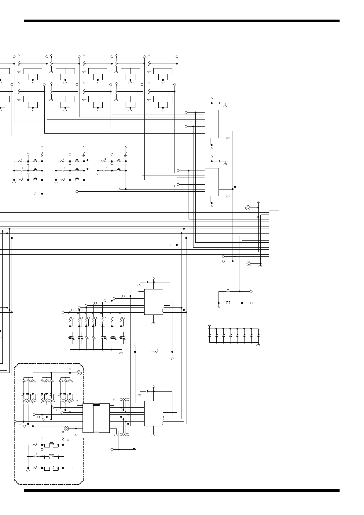
fig.d-panel.eps@R
D+3.3 D+3.3
D+3.3
GND
D+3.3
GND
D+3.3
GND
D+3.3
GND
D+3.3
GND
D+3.3
GND
D+3.3
GND
D+3.3
GND
D+3.3
GND
D+3.3
GND
PDGND
GND
D+3.3
GND
PD+3.3
D+3.3
GND
GND
D+3.3
GND
E-LEVEL
E-LEVEL
EQ-LEVEL
EQ-LEVEL
PRESENCE PRESENCE
TREBLETREBLE
ANTI-FB ANTI-FB
MIDMID
GND
GND
INPUT-SW
D+3.3
LEDD3
EXIT
MEMORY
GND
ND
ND GND GND GND GND GND
GND
GNDGND
GNDGND
MPXP2-Y
MPXP2-Y
MPXP1-Y
MPXP1-Y
MPXP1-X
MPXP1-X
MPXP2-X
MPXP2-X
GND
GND
GND
D+3.3
LEDD2
LEDD2
LEDD1
LED-RCKLED-RCK
LED-RCK
LED-RCK
LEDXGLEDXG
LEDXG
LEDXG
LED-SCKLED-SCK
LED-SCK
LED-SCKLED-SCK
AC-REZAC-REZ
COMP COMP
TIMETIME
BASS BASS
OUT-LEVEL
OUT-LEVEL
AMBIENCE
AMBIENCE
PEDAL-SW
PD+3.3
LEDD0
GND
PEDAL-SW
D+3.3
GND GND
GND
NOTCH
GND
ADMPX-B
ADMPX-B
ADMPX-A
ADMPX-A
D+3.3
GND
PD+3.3
PDGND
GND
D+3.3
SKPFACA010SW101
1
23
4
SKPFACA010SW102
1
23
4
SKPFACA010SW103
1
23
4
20
20
SW16
EVPAWCD4A
12
SW17
EVPAWCD4A
12
27k
R16
27k
R20
VR2
RD901F-40-125F-B50K-0CD
13
2
RD901F-40-125F-B50K-0CD
VR2
10
RD901F-40-125F-B50K-0CD
VR2
20
VR3
RD901F-40-125F-B50K-0CD
1
3
2
RD901F-40-125F-B50K-0CD
VR3
10
RD901F-40-125F-B50K-0CD
VR3
20
VR4
RD901F-40-125F-B50K-0CD
13
2
RD901F-40-125F-B50K-0CD
VR4
10
RD901F-40-125F-B50K-0CD
VR4
20
VR5
RD901F-40-125F-B50K-0CD
13
2
RD901F-40-125F-B50K-0CD
VR5
10
RD901F-40-125F-B50K-0CD
VR5
20
VR6
RD901F-40-125F-B50K-0CD
13
2
RD901F-40-125F-B50K-0CD
VR6
10
RD901F-40-125F-B50K-0CD
VR6
20
VR8
RV09BDF-40E1-125F-B50K
13
2
RV09BDF-40E1-125F-B50K
VR8
10
RV09BDF-40E1-125F-B50K
VR8
20
VR9
RV09BDF-40E1-125F-B50K
1
3
2
RV09BDF-40E1-125F-B50K
VR9
10
RV09BDF-40E1-125F-B50K
VR9
20
VR10
RV09BDF-40E1-125F-B50K
13
2
RV09BDF-40E1-125F-B50K
VR10
10
RV09BDF-40E1-125F-B50K
VR10
20
VR11
RV09BDF-40E1-125F-B50K
13
2
RV09BDF-40E1-125F-B50K
VR11
10
RV09BDF-40E1-125F-B50K
VR11
20
VR12
RV09BDF-40E1-125F-B50K
1
3
2
RV09BDF-40E1-125F-B50K
VR12
10
RV09BDF-40E1-125F-B50K
VR12
20
0.1uFC9
22FMN-STK-A (LF)(SN)
CN2
1
2
3
4
5
6
7
8
9
10
11
12
13
14
15
16
17
18
19
20
21
22
0.1uFC7
IC7
TC74VHC595FK
SI
14
_SCLR
10
_G
13
SCK
11
RCK
12
GND
8
QA
15
QB
1
QC
2
QD
3
QE
4
QF
5
QG
6
QH
7
QH-
9
VCC
16
100
R57
19-226SURSYGC/S530-A3/E2/TR8LED19
4A(G)
3 A(R)2K(R)
1K(G)
L-7104SRTLED20
1A2
K
L-7104SRT
LED21
1A2K
220
R44
220
R45
220
R48
19-226SURSYGC/S530-A3/E2/TR8LED22
4A(G)
3A(R)2
K(R)1K(G)
IC6
TC74VHC595FK
SI
14
_SCLR
10
_G
13
SCK
11
RCK
12
GND
8
QA
15
QB
1
QC
2
QD
3
QE
4
QF
5
QG
6
QH
7
QH-
9
VCC
16
56k
R110
27k
R111
12k
R112
27k
R113
CN101
1
2
3
4
5
6
8
9
10
11
12
7
0.1uFC8
27k
R52
0.1uFC6
220R49
19-226SURSYGC/S530-A3/E2/TR8LED23
4A(G)
3A(R)2K(R)
1K(G)
220
R51
19-226SURSYGC/S530-A3/E2/TR8LED24
4A(G)
3 A(R)
2
K(R)
1K(G)
L-T67FRGBCT-HL
LED101
2
A
4
K(BLU)
3 K(GRN)
1
K(RED)
L-T67FRGBCT-HL
LED102
2
A
4 K(BLU)
3
K(GRN)
1 K(RED)
L-T67FRGBCT-HL
LED103
2
A
4 K(BLU)
3 K(GRN)
1 K(RED)
19-226SURSYGC/S530-A3/E2/TR8LED18
4A(G)
3A(R)2K(R)
1K(G)
TP1 TP2 TP3 TP4 TP5 TP6
TP7 TP8 TP9 TP10 TP11 TP12
SW12
EVPAWCD4A
12
56k
R13
27k
R14
12k
R15
SW10
EVPAWCD4A
12
SW11
EVPAWCD4A
12
TP22
TP23
TP24
SW15
EVPAWCD4A
12
56k
R17
27k
R18
12k
R19
SW13
EVPAWCD4A
12
SW14
EVPAWCD4A
12
TP25
TP26
TP27
56k
R42
27k
R43
SW18
EVPAWCD4A
12
SW19
EVPAWCD4A
12
TP28
TP29
TP30
TP31
TP32
TP33
TP37
TP38
TP39
TP46
TP47
TP48
TP51
TP110
TP111
TP112
TP113
TP114
TP115
TP116
TP117
TP118
TP119
TP120
TP121
TP122
TP123
TP124
TP125
TP126
TP127
TP128
TP129
TP130
TP131
TP132
TP133
TP134
TP135
TP136
TP137
TP138
TP139
TP140
TP141
TP142
TP143
TP144
TP145
TP146
TP147
TP148
TP149
TP150
TP151
TP152
C10
10uF
16V
C11
10uF
16V
C12
10uF
16V
C13
10uF
16V
C14
10uF
16V
C15
10uF
16V
C16
10uF
16V
C17
10uF
16V
1kR46
1k
R47
SN74LV4052APWR
IC8
9
B
10
A
2
2Y
14
1X
2X
15
16
VCC
3
YCOM
7
VEE
1Y
5
3Y
4
INH
6
1
0Y
XCOM
13
11
3X
0X
12
GND
8
SN74LV4052APWR
IC9
9
B
10
A
2
2Y
14
1X
2X
15
16
VCC
3
YCOM
7
VEE
1Y
5
3Y
4
INH
6
1
0Y
XCOM
13
11
3X
0X
12
GND
8
CN1
1
2
3
4
5
6
8
9
10
11
12
7
TP162
TP163
TP164
TP165
TP166
TP167
TP168
TP169
TP170
TP173
330R101
330
R104
330
R107
470
R109
470
R106
470
R103
2.7k
R105
2.7k
R108
2.7k
R102
[DLY TYPE]
[CHORUS]
[AB-TYPE]
[ON/OFF]
[AB-OUT]
[MENU]
[MID]
B] [AC-REZ]
[TREBLE] [PRESENCE] [LEVEL]
[COMP]
(DLY/CHO)[TIME] (DLY/CHO)[E.LEVEL]
[OUT-LEVEL]
[AMBIENCE]
[EXIT]
[MEMORY]
[ (up)]
[
(down)]
[ON/OFF]
[XLR
]
[LINE]
[AB-OUT]
[MENU
]
[BOOST]
[DELAY]
[TUNER]
PEDAL BOARD
To MAIN BOARD CN2
[MEMORY]
[EXIT
]
(EQ) (EQ) (EQ) (EQ)
[BOOST] [DELAY] [TUNER]
AD-10 RIBBON CABLE
12P L=40x6x6 P=2.0
AD-10Sep. 2017
29
 Loading...