

Page 1
TS2576
3A / 52KHz Buck Switching Regulator
1/8 Version: A07
TO-220-5L
TO-263-5L
(D2PAK)
General Description
TS2576 Series are step-down switching regulators with all required active functions. It is capable of driving 3A load
with excellent line and load regulations. These devices are available in fixed output voltages of 3.3V, 5V and
adjustable output version.
TS2576 series operates at a switching frequency of 52kHz thus allowing smaller sized filter components than what
would be needed with lower frequency switching regulators. It substantially not only reduces the area of board size
but also the size of heat sink, and in some cases no heat sink is required. The ±4% tolerance on output voltage within
specified input voltages and output load conditions is guaranteed. Also, the oscillator frequency accuracy is within
±10%. External shutdown is included. Featuring 70µA (typical) standby current. The output switch includes cycle-bycycle current limiting, as well as thermal shutdown for full protection under fault conditions.
Ordering Information
Part No.
Package
Packing
TS2576CZ5xx C0
TO-220-5L
50pcs / Tube
TS2576CM5xx RN
TO-263-5L
800pcs / 13” Reel
Note: Where xx denotes voltage option, available are
50= 5.0V
33= 3.3V
Leave blank for adjustable version
Features
● Output Voltage: 3.3V, 5V & Adjustable version
● Adjustable Output Voltage Range 1.23V~37V ±4%
● 52kHz fixed switching frequency
● Voltage Mode Non-synchronous PWM control
● Thermal Shutdown and Current Limit Protection
● ON/OFF Shutdown Control Input
● High Efficiency
● Short Circuit Protect (SCP)
● Operating Voltage Can be up to 40V
● Output Load Current 3A
● Low Power Standby Mode
● P+ Product Enhancement Tested
Application
● Simple High-efficiency Step down Regulator
● On-Card Switching Regulators
● Positive to Negative Converter
Absolute Maximum Rating
Parameter
Symbol
Limit
Unit
Maximum Supply Voltage
VCC
+45
V
Recommend Operating Supply Voltage
VOP
4.5 to 40
V
SW, EN Pin Input Voltage
VSW, VEN
-0.3 to +25
V
Feedback Pin Voltage
VFB
-0.3 to +25
V
Power Dissipation
PD
Internally Limited
W
Output Voltage to Ground
V
OUT
-1
V
Storage Temperature Range
TST
-65 to +150
o
C
Operating Temperature Range
TOP
-40 to +125
o
C
ESD Susceptibility (HBM)
2 kV
Pin Definition:
1. Input
2. SW Output
3. Ground
4. Feedback
5. Enable
Page 2
TS2576
3A / 52KHz Buck Switching Regulator
2/8 Version: A07
Thermal Information
Parameter
Symbol
Maximum
Unit
TO-220-5L
2
Thermal Resistance (Junction to Case)
TO-263-5L
ӨJC
2
o
C/W
TO-220-5L
65 (note 1)
Thermal Resistance (Junction to Ambient)
TO-263-5L
Ө
JA
50 (note 2)
o
C/W
Note1: ӨJA is measured on the PCB with minimum copper area.
Note2: ӨJA is measured with the PCB copper area (need connect to GROUND pins) of approximately 0.5 in2
Electrical Specifications (All Output Voltage Version)
(Ta = 25oC unless otherwise noted, VIN=12V for 3.3V, 5V, Adjustable version. I
LOAD
=0.5A)
Parameter
Symbol
Test Condition
Min
Typ
Max
Unit
Output Feedback
VFB
4.5V≤ V
IN
≤40V
0.2A≤ I
LOAD
≤3A
1.180
1.23
1.280
V
Efficiency
ADJ
η
V
IN
=12V, I
LOAD
=3A
--
75
--
%
Output Feedback
VFB
4.75V≤ V
IN
≤40V
0.2A≤ I
LOAD
≤3A
3.135
3.3V
3.465
V
Efficiency
3.3V
η
V
IN
=12V, I
LOAD
=3A
--
75
--
%
Output Feedback
VFB
7V≤ V
IN
≤40V
0.2A≤ I
LOAD
≤3A
4.75
5
5.25
V
Efficiency
5V
η
V
IN
=12V, I
LOAD
=3A
--
77
--
%
Feedback Bias Current
IFB
V
OUT
= 5V (Adjustable Version)
--
50
100
nA
Oscillator Frequency
F
OSC
47
52
58
KHz
Soft-Start Time
TSS
Rising edge of EN on to ICL
-- 3 --
mS
Current Limit
ICL
Pear Current, no outside circuit
VFB =0V force driver on
5.9
--
--
A
Saturation Voltage
V
SAT
I
OUT
=3A, No outside circuit
VFB =0V force driver on
--
1.4
1.8
V
VIL
Low (regulator ON)
--
1.2
1.0
ON/OFF Pin Logic Input Threshold
Voltage
VIH
High (regulator OFF)
2.2
1.4
--
V
IL
V
LOGIC
=5V (OFF)
--
12
30
ON/OFF Pin Logic Input Current
IH
V
LOGIC
=0V (ON)
-- 0 10
µA
Maximum Duty Cycle (ON)
VFB =0V force driver on
93
98
--
Maximum Duty Cycle (OFF)
DC
VFB =12V force driver off
-- 0 --
%
Quiescent Current
IQ
VFB =12V force driver off
-- 5 10
mA
ON/OFF pin=5V
--
200
Standby Quiescent Current
I
STBY
VIN =40V
--
70
250
µA
SW pin = 0
No outside circuit,
VFB =12V force driver off
--
0.3 2 mA
SW Pin Leakage
Current
SW pin = -1
I
SWL
VIN =12V
--
7.5
30
mA
Page 3
TS2576
3A / 52KHz Buck Switching Regulator
3/8 Version: A07
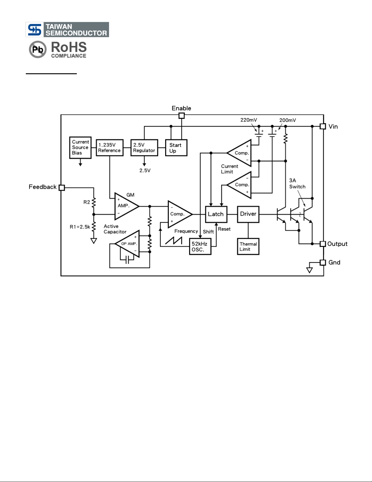
Block Diagram
Page 4

TS2576
3A / 52KHz Buck Switching Regulator
4/8 Version: A07
Typical Application Circuit
1. Adjustable Output Voltage Version
2. Fixed Output Voltage Version
3. Adjustable Output Voltage Version with Delayed Startup
Page 5

TS2576
3A / 52KHz Buck Switching Regulator
5/8 Version: A07
Pin Function Description
Vcc
This is the positive input supply for the IC switching regulator. A suitable input bypass capacitor must be presented at
this pin to minimize voltage transients and to supply the switching currents needed by the regulator.
Ground
Circuit ground
SW Output
Internal switch. The voltage at this pin switches between (+Vcc – Vsat) and approximately – 0.5V, with a duty cycle of
approximately Vout / Vcc. To minimize coupling to sensitive circuitry, the PC board copper area connected to this pin
should be minimized.
Feedback
Sense the regulated output voltage to complete the feedback loop.
Enable
Allows the switching regulator circuit to be shutdown using logic level signals thus dropping the total input supply
current to approximately 100uA. Pulling this pin below a threshold voltage of approximately 1.3V turns the regulator on,
and pulling this pin above 1.3V (up to a maximum of Vcc) shuts the regulator down. If this shutdown feature is not
needed, the EN pin can be wired to the ground pin.
Thermal Considerations
The TS2576 is available in two packages, a TO-220-5L and TO-263-5L.
The TO-220-5L package needs a heat sink under most conditions. The size of the heat sink depends on the input
voltage, the output voltage, the load current and the ambient temperature. The TS2576 junction temperature rises
above ambient temperature for a 3A load and different input and output voltages. The data for these curves was taken
with the TS2576CZ5 (TO-220-5L package) operating as a buck switching regulator in an ambient temperature of 25oC
(still air). These temperature rise numbers are all approximate and there are many factors that can affect these
temperatures. Higher ambient temperatures require more heat sinking.
The TO-263-5L surface mount package tab is designed to be soldered to the copper on a printed circuit board. The
copper and the board are the heat sink for this package and the other heat producing components, such as the catch
diode and inductor. The PC board copper area that the package is soldered to should be at least 0.8 in2, and ideally
should have 2 or more square inches of 2oz. Additional copper area improves the thermal characteristics, but with
copper areas greater than approximately 6 in2, only small improvements in heat dissipation are realized. If further
thermal improvements are needed, double sided, multilayer PC board with large copper areas and/or airflow are
recommended.
The TS2576 (TO-263-5L package) junction temperature rise above ambient temperature with a 3A load for various
input and output voltages. This data was taken with the circuit operating as a buck switching regulator with all
components mounted on a PC board to simulate the junction temperature under actual operating conditions. This
curve can be used for a quick check for the approximate junction temperature for various conditions, but be aware that
there are many factors that can affect the junction temperature. When load currents higher than 3A are used, double
sided or multilayer PC boards with large copper areas and/or airflow might be needed, especially for high ambient
temperatures and high output voltages.
For the best thermal performance, wide copper traces and generous amounts of printed circuit board copper should be
used in the board layout. (Once exception to this is the output (switch) pin, which should not have large areas of
copper.) Large areas of copper provide the best transfer of heat (lower thermal resistance) to the surrounding air, and
moving air lowers the thermal resistance even further.
Page 6

TS2576
3A / 52KHz Buck Switching Regulator
6/8 Version: A07
TO-220-5L Mechanical Drawing
Marking Diagram
Y
= Year Code
M
= Month Code
(A=Jan, B=Feb, C=Mar, D=Apl, E=May, F=Jun, G=Jul, H=Aug, I=Sep,
J=Oct, K=Nov, L=Dec)
L
= Lot Code
XXX
= Voltage Code
(3.3=3.3V, 5.0=5V)
= Package Code for Adjustable type
(CZ5 = TO-220-5L)
TO-220-5L DIMENSION
MILLIMETERS
INCHES
DIM
MIN
MAX
MIN
MAX
A
10.00
10.50
0.394
0.413
B
3.240
4.440
0.128
0.175
C
2.440
2.940
0.096
0.116
D
0.260
1.020
0.010
0.040
E
1.570
1.830
0.062
0.072
F
13.31
14.13
0.524
0.556
G
4.475
5.225
0.176
0.206
H
1.170
1.370
0.046
0.054
I
27.60
29.44
1.087
1.159
J
2.175
2.925
0.086
0.115
K
0.297
0.477
0.012
0.019
L
8.280
8.800
0.326
0.346
M
6.010
6.510
0.237
0.256
N
14.29
15.31
0.563
0.603
Page 7

TS2576
3A / 52KHz Buck Switching Regulator
7/8 Version: A07
TO-263-5L Mechanical Drawing
Marking Diagram
Y
= Year Code
M
= Month Code
(A=Jan, B=Feb, C=Mar, D=Apl, E=May, F=Jun, G=Jul, H=Aug, I=Sep,
J=Oct, K=Nov, L=Dec)
L
= Lot Code
XXX
= Voltage Code
(3.3=3.3V, 5.0=5V)
= Package Code for Adjustable type
(CM5 = TO-263-5L)
TO-263-5L DIMENSION
MILLIMETERS
INCHES
DIM
MIN
MAX
MIN
MAX
A
9.70
10.54
0.382
0.415
B
14.60
15.87
0.575
0.625
C
0.69
0.94
0.027
0.037
D
1.524
2.032
0.060
0.080
E
4.30
4.70
0.169
0.185
F
1.22
1.40
0.048
0.055
G
2.24
2.82
0.088
0.111
H
0.36
0.56
0.014
0.022
I
8.50
9.20
0.330
0.362
J
1.40 MAX
0.055 MAX
Page 8

TS2576
3A / 52KHz Buck Switching Regulator
8/8 Version: A07
Notice
Specifications of the products displayed herein are subject to change without notice. TSC or anyone on its behalf,
assumes no responsibility or liability for any errors or inaccuracies.
Information contained herein is intended to provide a product description only. No license, express or implied, to any
intellectual property rights is granted by this document. Except as provided in TSC’s terms and conditions of sale for
such products, TSC assumes no liability whatsoever, and disclaims any express or implied warranty, relating to sale
and/or use of TSC products including liability or warranties relating to fitness for a particular purpose, merchantability,
or infringement of any patent, copyright, or other intellectual property right.
The products shown herein are not designed for use in medical, life-saving, or life-sustaining applications. Customers
using or selling these products for use in such applications do so at their own risk and agree to fully indemnify TSC for
any damages resulting from such improper use or sale.
 Loading...