

Page 1

M
MC9S08QE128
MC9S08QE96
MC9S08QE64
Reference Manual
HCS08
Microcontrollers
MC9S08QE128RM
Rev. 2
6/2007
Related Documentation:
• MC9S08QE128 (Data Sheet)
Contains pin assignments and diagrams, all electrical
specifications, and mechanical drawing outlines.
Find the most current versions of all documents at:
http://www.freescale.com
freescale.com
Page 2

Page 3

MC9S08QE128 Series Features
I2C
Schmitt Trigger
Local Interconnect Network (LIN)
8-Bit HCS08 Central Processor Unit (CPU)
• Up to 50.33-MHz HCS08 CPU from 3.6 V to 2.1 V, and
20-MHz CPU at 2.1 V to 1.8 V across temperature range
of –40˚C to 85˚C
• HC08 instruction set with added BGND instruction
• Support for up to 32 interrupt/reset sources
On-Chip Memory
• Flash read/program/erase over full operating voltage and
temperature
• Random-access memory (RAM)
• Security circuitryto prevent unauthorized access to RAM
and flash contents
Power-Saving Modes
• Two very low power stop modes, one of which allows
limited use of peripherals
• Reduced power wait mode
• Peripheral clock enable register can disable clocks to
unused modules, thereby reducing currents; allows clocks
to remain enabled to specific peripherals in stop3 mode
• Very low power external oscillator that can be used in
stop3 mode to provide accurate clock source to active
peripherals
• Very low power real time counter for use in run, wait, and
stop modes with internal and external clock sources
•6μs typical wake up time from stop3 mode
Clock Source Options
• Oscillator (XOSC) — Loop-control Pierce oscillator;
crystal or ceramic resonator range of 31.25 kHz to
38.4 kHz or 1 MHz to 16 MHz
• Internal Clock Source (ICS) — Internal clock source
module containing a frequency-locked-loop (FLL)
controlled by internal or external reference; precision
trimming of internal reference allows0.2%resolution and
2%deviationovertemperatureandvoltage;supportsCPU
frequencies from 2 MHz to 50.33 MHz
System Protection
• Watchdog computer operating properly (COP) reset with
option to run from dedicated 1-kHz internal clock source
or bus clock
• Low-voltage detection with reset or interrupt; selectable
trip points
• Illegal opcode detection with reset
• Flash block protection
Development Support
• Single-wire background debug interface
• Breakpoint capability to allow single breakpoint setting
duringin-circuit debugging (plus two more breakpoints in
on-chip debug module)
• On-chip in-circuit emulator (ICE) debug module
containing three comparators and nine trigger modes.
EightdeepFIFO for storing change-of-flow addresses and
event-only data. Debug module supports both tag and
force breakpoints.
Peripherals
• ADC — 24-channel, 12-bit resolution; 2.5 μs conversion
time; automatic compare function; 1.7 mV/°C
temperature sensor; internal bandgap reference channel;
operation in stop3; fully functional from 3.6 V to 1.8 V
• ACMPx — Two analog comparators with selectable
interrupt on rising, falling, or either edge of comparator
output; compare option to fixed internal bandgap
reference voltage; outputs can be optionally routed to
TPM module; operation in stop3
• SCIx — Two full duplex non-return to zero (NRZ); LIN
master extended break generation; LIN slave extended
break detection; wake up on active edge
• SPIx— Two serial peripheral interfaces with full-duplex
or single-wire bidirectional; double-buffered transmit and
receive; master or slave mode; MSB-first or LSB-first
shifting
• IICx — Two IICs with; up to 100 kbps with maximum
bus loading; multi-master operation; programmable slave
address; interrupt driven byte-by-byte data transfer;
supports broadcast mode and 10 bit addressing
• TPMx — One 6-channel (TPM3) and two 3-channel
(TPM1 and TPM2); Selectable input capture, output
compare, or buffered edge- or center-aligned PWM on
each channel
• RTC — (Real-time counter) 8-bit modulus counter with
binary or decimal based prescaler; external clock source
for precise time base, time-of-day, calendar or task
scheduling functions; free running on-chip low power
oscillator (1 kHz) for cyclic wake-up without external
components; runs in all MCU modes
Input/Output
• 70 GPIOs and 1 input-only and 1 output only pin
• 16 KBI interrupts with selectable polarity
• Hysteresis and configurable pull up device on all input
pins; configurable slew rate and drive strength on all
output pins.
• SET/CLR registers on 16 pins (PTC and PTE)
Package Options
• 80-LQFP, 64-LQFP, 48-QFN, 44-QFP, 32-LQFP
Page 4

Page 5

MC9S08QE128 Reference Manual
Covers MC9S08QE128
MC9S08QE96
MC9S08QE64
MC9S08QE128RM
Rev. 2
6/2007
Freescale™ and the Freescale logo are trademarks of Freescale Semiconductor, Inc.
© Freescale Semiconductor, Inc., 2007. All rights reserved.
Get the latest version from freescale.com
Page 6

Revision History
To provide the most up-to-date information, the revision of our documents on the World Wide Web will be
the most current. Your printed copy may be an earlier revision. To verify you have the latest information
available, refer to:
http://freescale.com/
The following revision history table summarizes changes contained in this document.
Revision
Number
1 30 Apr 2007 Initial preliminary release
2 25 Jun 2007 Initial public release
Revision
Date
Description of Changes
© Freescale Semiconductor, Inc., 2007. All rights reserved.
This product incorporates SuperFlash
®
Technology licensed from SST.
Page 7

List of Chapters
Chapter 1 Device Overview..............................................................................19
Chapter 2 Pins and Connections.....................................................................25
Chapter 3 Modes of Operation.........................................................................39
Chapter 4 Memory.............................................................................................51
Chapter 5 Resets, Interrupts, and General System Control..........................89
Chapter 6 Parallel Input/Output Control........................................................111
Chapter 7 Keyboard Interrupt (S08KBIV2)....................................................139
Chapter 8 Central Processor Unit (S08CPUV4)............................................145
Chapter 9 Analog Comparator 3V (ACMPVLPV1)........................................167
Chapter 10 Analog-to-Digital Converter (S08ADC12V1)................................175
Chapter 11 Internal Clock Source (S08ICSV3) ...............................................203
Chapter 12 Inter-Integrated Circuit (S08IICV2)...............................................217
Chapter 13 Real-Time Counter (S08RTCV1)...................................................237
Chapter 14 Serial Communications Interface (S08SCIV4).............................247
Chapter 15 Serial Peripheral Interface (S08SPIV3) ........................................267
Chapter 16 Timer/Pulse-Width Modulator (S08TPMV3).................................283
Chapter 17 Development Support ...................................................................307
Chapter 18 Debug Module (DBG) (128K).........................................................321
MC9S08QE128 MCU Series Reference Manual, Rev. 2
Freescale Semiconductor 7
Page 8

Contents
Section Number Title Page
Chapter 1
Device Overview
1.1 Devices in the MC9S08QE128 Series .............................................................................................19
1.2 MCU Block Diagram ......................................................................................................................20
1.3 System Clock Distribution ..............................................................................................................23
Chapter 2
Pins and Connections
2.1 Device Pin Assignment ...................................................................................................................25
2.2 Recommended System Connections ...............................................................................................31
2.2.1 Power ................................................................................................................................33
2.2.2 Oscillator ...........................................................................................................................33
2.2.3
2.2.4 Background / Mode Select (BKGD/MS) ..........................................................................34
2.2.5 ADC Reference Pins (V
2.2.6 General-Purpose I/O and Peripheral Ports ........................................................................35
RESET and RSTO ............................................................................................................33
REFH
, V
) ..............................................................................35
REFL
Chapter 3
Modes of Operation
3.1 Introduction .....................................................................................................................................39
3.2 Features ...........................................................................................................................................39
3.3 Run Mode ........................................................................................................................................39
3.3.1 Low Power Run Mode (LPRun) .......................................................................................39
3.4 Active Background Mode ................................................................................................................41
3.5 Wait Mode .......................................................................................................................................42
3.5.1 Low Power Wait Mode (LPWait) ......................................................................................42
3.6 Stop Modes ......................................................................................................................................42
3.6.1 Stop2 Mode .......................................................................................................................43
3.6.2 Stop3 Mode .......................................................................................................................44
3.6.3 Active BDM Enabled in Stop Mode .................................................................................45
3.6.4 LVD Enabled in Stop Mode ..............................................................................................45
3.6.5 Stop modes in Low Power Run Mode ..............................................................................45
3.7 Mode Selection ................................................................................................................................45
3.7.1 On-Chip Peripheral Modules in Stop and Low Power Modes ..........................................48
Chapter 4
Memory
4.1 MC9S08QE128 Series Memory Map .............................................................................................51
4.2 Reset and Interrupt Vector Assignments .........................................................................................53
MC9S08QE128 MCU Series Reference Manual, Rev. 2
Freescale Semiconductor 9
Page 9

Section Number Title Page
4.3 Register Addresses and Bit Assignments ........................................................................................55
4.4 Memory Management Unit .............................................................................................................63
4.4.1 Features .............................................................................................................................63
4.4.2 Register Definition ............................................................................................................63
4.4.3 Functional Description ......................................................................................................66
4.5 RAM ................................................................................................................................................69
4.6 Flash ................................................................................................................................................69
4.6.1 Features .............................................................................................................................70
4.6.2 Register Descriptions ........................................................................................................70
4.6.3 Functional Description ......................................................................................................77
4.6.4 Operating Modes ...............................................................................................................86
4.6.5 Flash Module Security ......................................................................................................86
4.6.6 Resets ................................................................................................................................88
Chapter 5
Resets, Interrupts, and General System Control
5.1 Introduction .....................................................................................................................................89
5.2 Features ...........................................................................................................................................89
5.3 MCU Reset ......................................................................................................................................89
5.4 Computer Operating Properly (COP) Watchdog .............................................................................90
5.5 Interrupts .........................................................................................................................................91
5.5.1 Interrupt Stack Frame .......................................................................................................92
5.5.2 External Interrupt Request (IRQ) Pin ...............................................................................92
5.5.3 Interrupt Vectors, Sources, and Local Masks ....................................................................93
5.6 Low-Voltage Detect (LVD) System ................................................................................................96
5.6.1 Power-On Reset Operation ...............................................................................................96
5.6.2 Low-Voltage Detection (LVD) Reset Operation ...............................................................96
5.6.3 Low-Voltage Detection (LVD) Interrupt Operation ..........................................................96
5.6.4 Low-Voltage Warning (LVW) Interrupt Operation ...........................................................96
5.7 Peripheral Clock Gating ..................................................................................................................96
5.8 Reset, Interrupt, and System Control Registers and Control Bits ...................................................98
5.8.1 Interrupt Pin Request Status and Control Register (IRQSC) ............................................98
5.8.2 System Reset Status Register (SRS) .................................................................................99
5.8.3 System Background Debug Force Reset Register (SBDFR) ..........................................100
5.8.4 System Options Register 1 (SOPT1) ..............................................................................101
5.8.5 System Options Register 2 (SOPT2) ..............................................................................102
5.8.6 System Device Identification Register (SDIDH, SDIDL) ..............................................103
5.8.7 System Power Management Status and Control 1 Register (SPMSC1) .........................104
5.8.8 System Power Management Status and Control 2 Register (SPMSC2) .........................105
5.8.9 System Power Management Status and Control 3 Register (SPMSC3) .........................106
5.8.10 System Clock Gating Control 1 Register (SCGC1) ........................................................107
5.8.11 System Clock Gating Control 2 Register (SCGC2) ........................................................108
MC9S08QE128 MCU Series Reference Manual, Rev. 2
10 Freescale Semiconductor
Page 10

Section Number Title Page
Chapter 6
Parallel Input/Output Control
6.1 Port Data and Data Direction ........................................................................................................111
6.2 Pull-up, Slew Rate, and Drive Strength .........................................................................................112
6.2.1 Port Internal Pull-Up Enable ...........................................................................................112
6.2.2 Port Slew Rate Enable ....................................................................................................112
6.2.3 Port Drive Strength Select ...............................................................................................112
6.3 Port Data Set, Clear and Toggle Data Registers ............................................................................113
6.3.1 Port Data Set Registers ...................................................................................................114
6.3.2 Port Data Clear Registers ................................................................................................114
6.3.3 Port Data Toggle Register ...............................................................................................114
6.4 Pin Behavior in Stop Modes ..........................................................................................................114
6.5 Parallel I/O and Pin Control Registers ..........................................................................................114
6.5.1 Port A Registers ..............................................................................................................115
6.5.2 Port B Registers ..............................................................................................................117
6.5.3 Port C Registers ..............................................................................................................119
6.5.4 Port D Registers ..............................................................................................................123
6.5.5 Port E Registers ...............................................................................................................125
6.5.6 Port F Registers ...............................................................................................................129
6.5.7 Port G Registers ..............................................................................................................131
6.5.8 Port H Registers ..............................................................................................................133
6.5.9 Port J Registers ...............................................................................................................135
Chapter 7
Keyboard Interrupt (S08KBIV2)
7.1 Introduction ...................................................................................................................................139
7.1.1 KBI Clock Gating ...........................................................................................................139
7.1.2 Features ...........................................................................................................................139
7.1.3 Modes of Operation ........................................................................................................139
7.1.4 Block Diagram ................................................................................................................140
7.2 External Signal Description ..........................................................................................................140
7.3 Register Definition ........................................................................................................................141
7.3.1 KBI Interrupt Status and Control Register (KBIxSC) ....................................................141
7.3.2 KBI Interrupt Pin Select Register (KBIxPE) ..................................................................142
7.3.3 KBI Interrupt Edge Select Register (KBIxES) ...............................................................142
7.4 Functional Description ..................................................................................................................142
7.4.1 Edge Only Sensitivity .....................................................................................................143
7.4.2 Edge and Level Sensitivity ..............................................................................................143
7.4.3 Pull-Up/Pull-Down Resistors ..........................................................................................143
7.4.4 Keyboard Interrupt Initialization ....................................................................................143
MC9S08QE128 MCU Series Reference Manual, Rev. 2
Freescale Semiconductor 11
Page 11

Section Number Title Page
Chapter 8
Central Processor Unit (S08CPUV4)
8.1 Introduction ...................................................................................................................................145
8.1.1 Features ...........................................................................................................................145
8.2 Programmer’s Model and CPU Registers .....................................................................................146
8.2.1 Accumulator (A) .............................................................................................................146
8.2.2 Index Register (H:X) .......................................................................................................146
8.2.3 Stack Pointer (SP) ...........................................................................................................147
8.2.4 Program Counter (PC) ....................................................................................................147
8.2.5 Condition Code Register (CCR) .....................................................................................147
8.3 Addressing Modes .........................................................................................................................149
8.3.1 Inherent Addressing Mode (INH) ...................................................................................149
8.3.2 Relative Addressing Mode (REL) ...................................................................................149
8.3.3 Immediate Addressing Mode (IMM) ..............................................................................149
8.3.4 Direct Addressing Mode (DIR) ......................................................................................150
8.3.5 Extended Addressing Mode (EXT) ................................................................................150
8.3.6 Indexed Addressing Mode ..............................................................................................150
8.4 Special Operations .........................................................................................................................151
8.4.1 Reset Sequence ...............................................................................................................151
8.4.2 Interrupt Sequence ..........................................................................................................151
8.4.3 Wait Mode Operation ......................................................................................................152
8.4.4 Stop Mode Operation ......................................................................................................152
8.4.5 BGND Instruction ...........................................................................................................153
8.5 HCS08 Instruction Set Summary ..................................................................................................155
Chapter 9
Analog Comparator 3V (ACMPVLPV1)
9.1 Introduction ...................................................................................................................................167
9.1.1 ACMP Configuration Information ..................................................................................167
9.1.2 ACMP/TPM Configuration Information .........................................................................167
9.1.3 ACMP Clock Gating .......................................................................................................167
9.1.4 Interrupt Vectors ..............................................................................................................168
9.1.5 Features ...........................................................................................................................170
9.1.6 Modes of Operation ........................................................................................................170
9.1.7 Block Diagram ................................................................................................................170
9.2 External Signal Description ..........................................................................................................171
9.3 Register Definition ........................................................................................................................171
9.3.1 ACMPx Status and Control Register (ACMPxSC) .........................................................172
9.4 Functional Description ..................................................................................................................173
MC9S08QE128 MCU Series Reference Manual, Rev. 2
12 Freescale Semiconductor
Page 12

Section Number Title Page
Chapter 10
Analog-to-Digital Converter (S08ADC12V1)
10.1 Introduction ...................................................................................................................................175
10.1.1 ADC Clock Gating ..........................................................................................................175
10.1.2 Module Configurations ...................................................................................................177
10.1.3 Features ...........................................................................................................................179
10.1.4 Block Diagram ................................................................................................................179
10.2 External Signal Description ..........................................................................................................180
10.2.1 Analog Power (V
10.2.2 Analog Ground (V
10.2.3 Voltage Reference High (V
10.2.4 Voltage Reference Low (V
10.2.5 Analog Channel Inputs (ADx) ........................................................................................181
10.3 Register Definition ........................................................................................................................181
10.3.1 Status and Control Register 1 (ADCSC1) ......................................................................181
10.3.2 Status and Control Register 2 (ADCSC2) ......................................................................183
10.3.3 Data Result High Register (ADCRH) .............................................................................184
10.3.4 Data Result Low Register (ADCRL) ..............................................................................184
10.3.5 Compare Value High Register (ADCCVH) ....................................................................185
10.3.6 Compare Value Low Register (ADCCVL) .....................................................................185
10.3.7 Configuration Register (ADCCFG) ................................................................................185
10.3.8 Pin Control 1 Register (APCTL1) ..................................................................................187
10.3.9 Pin Control 2 Register (APCTL2) ..................................................................................188
10.3.10Pin Control 3 Register (APCTL3) ..................................................................................189
10.4 Functional Description ..................................................................................................................190
10.4.1 Clock Select and Divide Control ....................................................................................190
10.4.2 Input Select and Pin Control ...........................................................................................191
10.4.3 Hardware Trigger ............................................................................................................191
10.4.4 Conversion Control .........................................................................................................191
10.4.5 Automatic Compare Function .........................................................................................194
10.4.6 MCU Wait Mode Operation ............................................................................................194
10.4.7 MCU Stop3 Mode Operation ..........................................................................................194
10.4.8 MCU Stop1 and Stop2 Mode Operation .........................................................................195
10.5 Initialization Information ..............................................................................................................195
10.5.1 ADC Module Initialization Example .............................................................................195
10.6 Application Information ................................................................................................................197
10.6.1 External Pins and Routing ..............................................................................................197
10.6.2 Sources of Error ..............................................................................................................199
) ..................................................................................................181
DDAD
) .................................................................................................181
SSAD
) ...................................................................................181
REFH
) .....................................................................................181
REFL
MC9S08QE128 MCU Series Reference Manual, Rev. 2
Freescale Semiconductor 13
Page 13

Section Number Title Page
Chapter 11
Internal Clock Source (S08ICSV3)
11.1 Introduction ...................................................................................................................................203
11.1.1 External Oscillator ..........................................................................................................203
11.1.2 Stop2 Mode Considerations ............................................................................................203
11.1.3 Features ...........................................................................................................................205
11.1.4 Block Diagram ................................................................................................................205
11.1.5 Modes of Operation ........................................................................................................206
11.2 External Signal Description ..........................................................................................................207
11.3 Register Definition ........................................................................................................................207
11.3.1 ICS Control Register 1 (ICSC1) .....................................................................................208
11.3.2 ICS Control Register 2 (ICSC2) .....................................................................................209
11.3.3 ICS Trim Register (ICSTRM) .........................................................................................209
11.3.4 ICS Status and Control (ICSSC) .....................................................................................210
11.4 Functional Description ..................................................................................................................212
11.4.1 Operational Modes ..........................................................................................................212
11.4.2 Mode Switching ..............................................................................................................214
11.4.3 Bus Frequency Divider ...................................................................................................215
11.4.4 Low Power Bit Usage .....................................................................................................215
11.4.5 DCO Maximum Frequency with 32.768 kHz Oscillator ................................................215
11.4.6 Internal Reference Clock ................................................................................................215
11.4.7 External Reference Clock ...............................................................................................216
11.4.8 Fixed Frequency Clock ...................................................................................................216
11.4.9 Local Clock .....................................................................................................................216
Chapter 12
Inter-Integrated Circuit (S08IICV2)
12.1 Introduction ...................................................................................................................................217
12.1.1 Module Configuration .....................................................................................................217
12.1.2 Interrupt Vectors ..............................................................................................................217
12.1.3 Features ...........................................................................................................................219
12.1.4 Modes of Operation ........................................................................................................219
12.1.5 Block Diagram ................................................................................................................220
12.2 External Signal Description ..........................................................................................................220
12.2.1 SCL — Serial Clock Line ...............................................................................................220
12.2.2 SDA — Serial Data Line ................................................................................................220
12.3 Register Definition ........................................................................................................................221
12.3.1 IIC Address Register (IICxA) .........................................................................................221
12.3.2 IIC Frequency Divider Register (IICxF) .........................................................................222
12.3.3 IIC Control Register (IICxC1) ........................................................................................224
12.3.4 IIC Status Register (IICxS) .............................................................................................225
12.3.5 IIC Data I/O Register (IICxD) ........................................................................................226
MC9S08QE128 MCU Series Reference Manual, Rev. 2
14 Freescale Semiconductor
Page 14

Section Number Title Page
12.3.6 IIC Control Register 2 (IICxC2) .....................................................................................227
12.4 Functional Description ..................................................................................................................228
12.4.1 IIC Protocol .....................................................................................................................228
12.4.2 10-bit Address .................................................................................................................232
12.4.3 General Call Address ......................................................................................................233
12.5 Resets ............................................................................................................................................233
12.6 Interrupts .......................................................................................................................................233
12.6.1 Byte Transfer Interrupt ....................................................................................................233
12.6.2 Address Detect Interrupt .................................................................................................233
12.6.3 Arbitration Lost Interrupt ................................................................................................233
12.7 Initialization/Application Information ..........................................................................................235
Chapter 13
Real-Time Counter (S08RTCV1)
13.1 Introduction ...................................................................................................................................237
13.1.1 ADC Hardware Trigger ..................................................................................................237
13.1.2 RTC Clock Sources .........................................................................................................237
13.1.3 RTC Modes of Operation ................................................................................................237
13.1.4 RTC Clock Gating ...........................................................................................................237
13.1.5 Interrupt Vector ...............................................................................................................238
13.1.6 Features ...........................................................................................................................240
13.1.7 Modes of Operation ........................................................................................................240
13.1.8 Block Diagram ................................................................................................................241
13.2 External Signal Description ..........................................................................................................241
13.3 Register Definition ........................................................................................................................241
13.3.1 RTC Status and Control Register (RTCSC) ....................................................................242
13.3.2 RTC Counter Register (RTCCNT) ..................................................................................243
13.3.3 RTC Modulo Register (RTCMOD) ................................................................................243
13.4 Functional Description ..................................................................................................................244
13.4.1 RTC Operation Example .................................................................................................245
13.5 Initialization/Application Information ..........................................................................................245
Chapter 14
Serial Communications Interface (S08SCIV4)
14.1 Introduction ...................................................................................................................................247
14.1.1 SCI Clock Gating ............................................................................................................247
14.1.2 Interrupt Vectors ..............................................................................................................247
14.1.3 Features ...........................................................................................................................250
14.1.4 Modes of Operation ........................................................................................................250
14.1.5 Block Diagram ................................................................................................................251
14.2 Register Definition ........................................................................................................................253
14.2.1 SCI Baud Rate Registers (SCIxBDH, SCIxBDL) ..........................................................253
MC9S08QE128 MCU Series Reference Manual, Rev. 2
Freescale Semiconductor 15
Page 15

Section Number Title Page
14.2.2 SCI Control Register 1 (SCIxC1) ...................................................................................254
14.2.3 SCI Control Register 2 (SCIxC2) ...................................................................................255
14.2.4 SCI Status Register 1 (SCIxS1) ......................................................................................256
14.2.5 SCI Status Register 2 (SCIxS2) ......................................................................................258
14.2.6 SCI Control Register 3 (SCIxC3) ...................................................................................259
14.2.7 SCI Data Register (SCIxD) .............................................................................................260
14.3 Functional Description ..................................................................................................................260
14.3.1 Baud Rate Generation .....................................................................................................260
14.3.2 Transmitter Functional Description ................................................................................261
14.3.3 Receiver Functional Description .....................................................................................262
14.3.4 Interrupts and Status Flags ..............................................................................................264
14.3.5 Additional SCI Functions ...............................................................................................265
Chapter 15
Serial Peripheral Interface (S08SPIV3)
15.1 Introduction ...................................................................................................................................267
15.1.1 SPI Clock Gating ............................................................................................................267
15.1.2 Interrupt Vector ...............................................................................................................267
15.1.3 Features ...........................................................................................................................269
15.1.4 Block Diagrams ..............................................................................................................269
15.1.5 SPI Baud Rate Generation ..............................................................................................271
15.2 External Signal Description ..........................................................................................................272
15.2.1 SPSCK — SPI Serial Clock ............................................................................................272
15.2.2 MOSI — Master Data Out, Slave Data In ......................................................................272
15.2.3 MISO — Master Data In, Slave Data Out ......................................................................272
15.2.4
15.3 Modes of Operation .......................................................................................................................273
15.3.1 SPI in Stop Modes ..........................................................................................................273
15.4 Register Definition ........................................................................................................................273
15.4.1 SPI Control Register 1 (SPIxC1) ....................................................................................273
15.4.2 SPI Control Register 2 (SPIxC2) ....................................................................................274
15.4.3 SPI Baud Rate Register (SPIxBR) ..................................................................................275
15.4.4 SPI Status Register (SPIxS) ............................................................................................276
15.4.5 SPI Data Register (SPIxD) ..............................................................................................277
15.5 Functional Description ..................................................................................................................278
15.5.1 SPI Clock Formats ..........................................................................................................278
15.5.2 SPI Interrupts ..................................................................................................................281
15.5.3 Mode Fault Detection .....................................................................................................281
SS — Slave Select ...........................................................................................................272
Chapter 16
Timer/Pulse-Width Modulator (S08TPMV3)
16.1 Introduction ...................................................................................................................................283
MC9S08QE128 MCU Series Reference Manual, Rev. 2
16 Freescale Semiconductor
Page 16

Section Number Title Page
16.1.1 ACMP/TPM Configuration Information .........................................................................283
16.1.2 TPM Clock Gating ..........................................................................................................283
16.1.3 Interrupt Vector ...............................................................................................................283
16.1.4 Features ...........................................................................................................................285
16.1.5 Modes of Operation ........................................................................................................285
16.1.6 Block Diagram ................................................................................................................286
16.2 Signal Description .........................................................................................................................288
16.2.1 Detailed Signal Descriptions ...........................................................................................288
16.3 Register Definition ........................................................................................................................292
16.3.1 TPM Status and Control Register (TPMxSC) ................................................................292
16.3.2 TPM-Counter Registers (TPMxCNTH:TPMxCNTL) ....................................................293
16.3.3 TPM Counter Modulo Registers (TPMxMODH:TPMxMODL) ....................................294
16.3.4 TPM Channel n Status and Control Register (TPMxCnSC) ..........................................295
16.3.5 TPM Channel Value Registers (TPMxCnVH:TPMxCnVL) ..........................................296
16.4 Functional Description ..................................................................................................................298
16.4.1 Counter ............................................................................................................................298
16.4.2 Channel Mode Selection .................................................................................................300
16.5 Reset Overview .............................................................................................................................303
16.5.1 General ............................................................................................................................303
16.5.2 Description of Reset Operation .......................................................................................303
16.6 Interrupts .......................................................................................................................................303
16.6.1 General ............................................................................................................................303
16.6.2 Description of Interrupt Operation ..................................................................................304
Chapter 17
Development Support
17.1 Introduction ...................................................................................................................................307
17.1.1 Forcing Active Background ............................................................................................307
17.1.2 DBG Clock Gating ..........................................................................................................307
17.1.3 Module Configuration .....................................................................................................307
17.1.4 Features ...........................................................................................................................308
17.2 Background Debug Controller (BDC) ..........................................................................................308
17.2.1 BKGD Pin Description ...................................................................................................309
17.2.2 Communication Details ..................................................................................................309
17.2.3 BDC Commands .............................................................................................................313
17.2.4 BDC Hardware Breakpoint .............................................................................................315
17.3 Register Definition ........................................................................................................................315
17.3.1 BDC Registers and Control Bits .....................................................................................316
17.3.2 System Background Debug Force Reset Register (SBDFR) ..........................................318
MC9S08QE128 MCU Series Reference Manual, Rev. 2
Freescale Semiconductor 17
Page 17

Section Number Title Page
Chapter 18
Debug Module (DBG) (128K)
18.1 Introduction ...................................................................................................................................321
18.1.1 Features ...........................................................................................................................321
18.1.2 Modes of Operation ........................................................................................................322
18.1.3 Block Diagram ................................................................................................................322
18.2 Signal Description .........................................................................................................................322
18.3 Memory Map and Registers ..........................................................................................................323
18.3.1 Module Memory Map .....................................................................................................323
18.3.2 324
18.3.3 Register Descriptions ......................................................................................................325
18.4 Functional Description ..................................................................................................................338
18.4.1 Comparator .....................................................................................................................338
18.4.2 Breakpoints .....................................................................................................................339
18.4.3 Trigger Selection .............................................................................................................339
18.4.4 Trigger Break Control (TBC) .........................................................................................340
18.4.5 FIFO ................................................................................................................................343
18.4.6 Interrupt Priority .............................................................................................................344
18.5 Resets ............................................................................................................................................344
18.6 Interrupts .......................................................................................................................................345
18.7 Electrical Specifications ................................................................................................................345
MC9S08QE128 MCU Series Reference Manual, Rev. 2
18 Freescale Semiconductor
Page 18
Chapter 1 Device Overview
The MC9S08QE128, MC9S08QE96, and MC9S08QE64 are members of the low-cost, low-power,
high-performance HCS08 Family of 8-bit microcontroller units (MCUs). All MCUs in the family use the
enhanced HCS08 core and are available with a variety of modules, memory sizes, memory types, and
package types.
1.1 Devices in the MC9S08QE128 Series
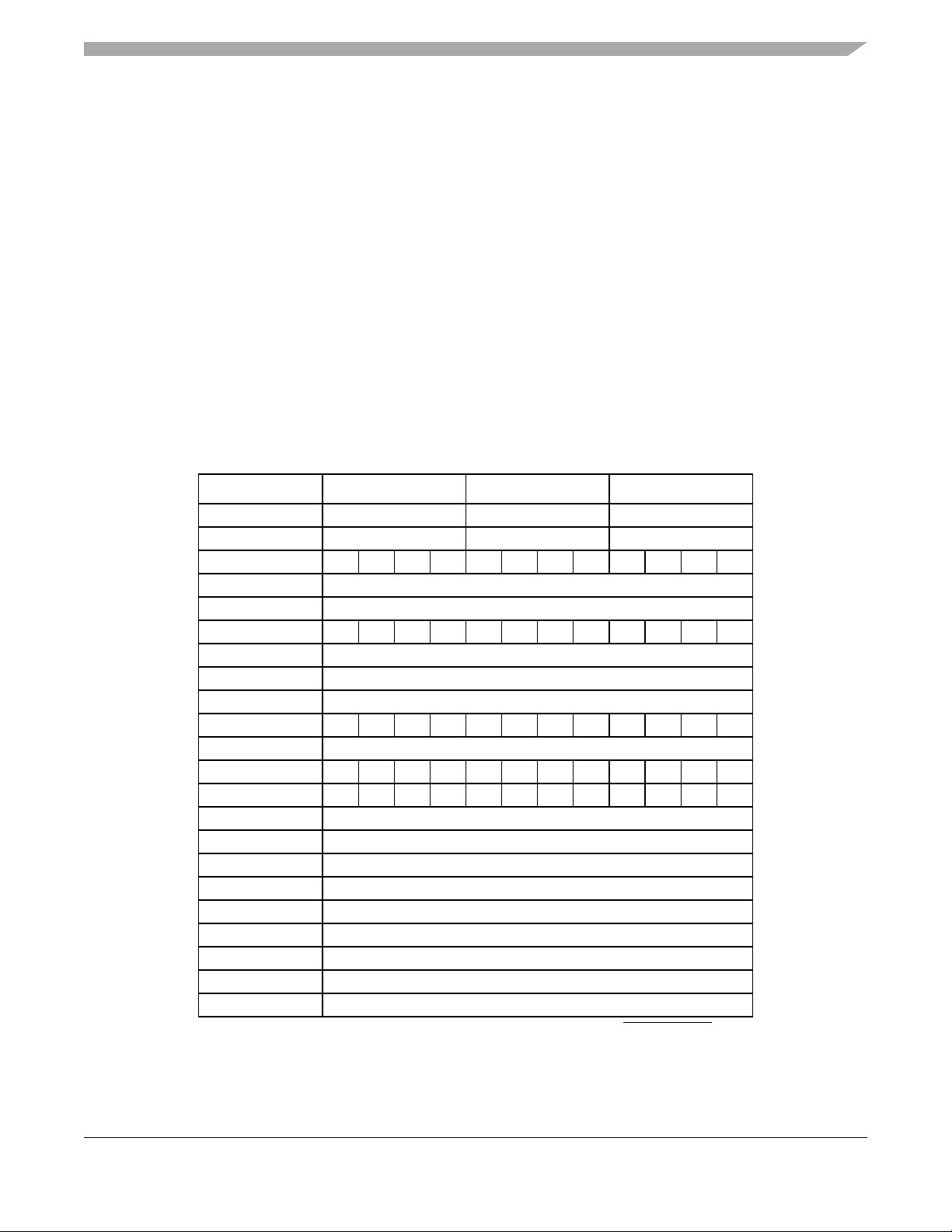
Table 1-1 summarizes the feature set available in the MC9S08QE128 Series of MCUs.
t
Table 1-1. MC9S08QE128 Series Features by MCU and Package
Feature MC9S08QE128 MC9S08QE96 MC9S08QE64
Flash size (bytes) 131,072 98,304 65,536
RAM size (bytes) 8064 6016 4096
Pin quantity 80 64 48 44 80 64 48 44 64 48 44 32
ACMP1 yes
ACMP2 yes
ADC channels 24 22 10 10 24 22 10 10 22 10 10 10
DBG yes
ICS yes
IIC1 yes
IIC2 yes yes no no yes yes no no yes no no no
IRQ yes
KBI 16 16 16 16 16 16 16 16 16 16 16 12
Port I/O
RTC yes
SCI1 yes
SCI2 yes
SPI1 yes
SPI2 yes
TPM1 channels 3
TPM2 channels 3
TPM3 channels 6
XOSC yes
1
1
PortI/O count does not include theinput only PTA5/IRQ/TPM1CLK/RESET orthe output
only PTA4/ACMP1O/BKGD/MS.
70 54 38 34 70 54 38 34 54 38 34 26
MC9S08QE128 MCU Series Reference Manual, Rev. 2
Freescale Semiconductor 19
Page 19

Chapter 1 Device Overview
1.2 MCU Block Diagram
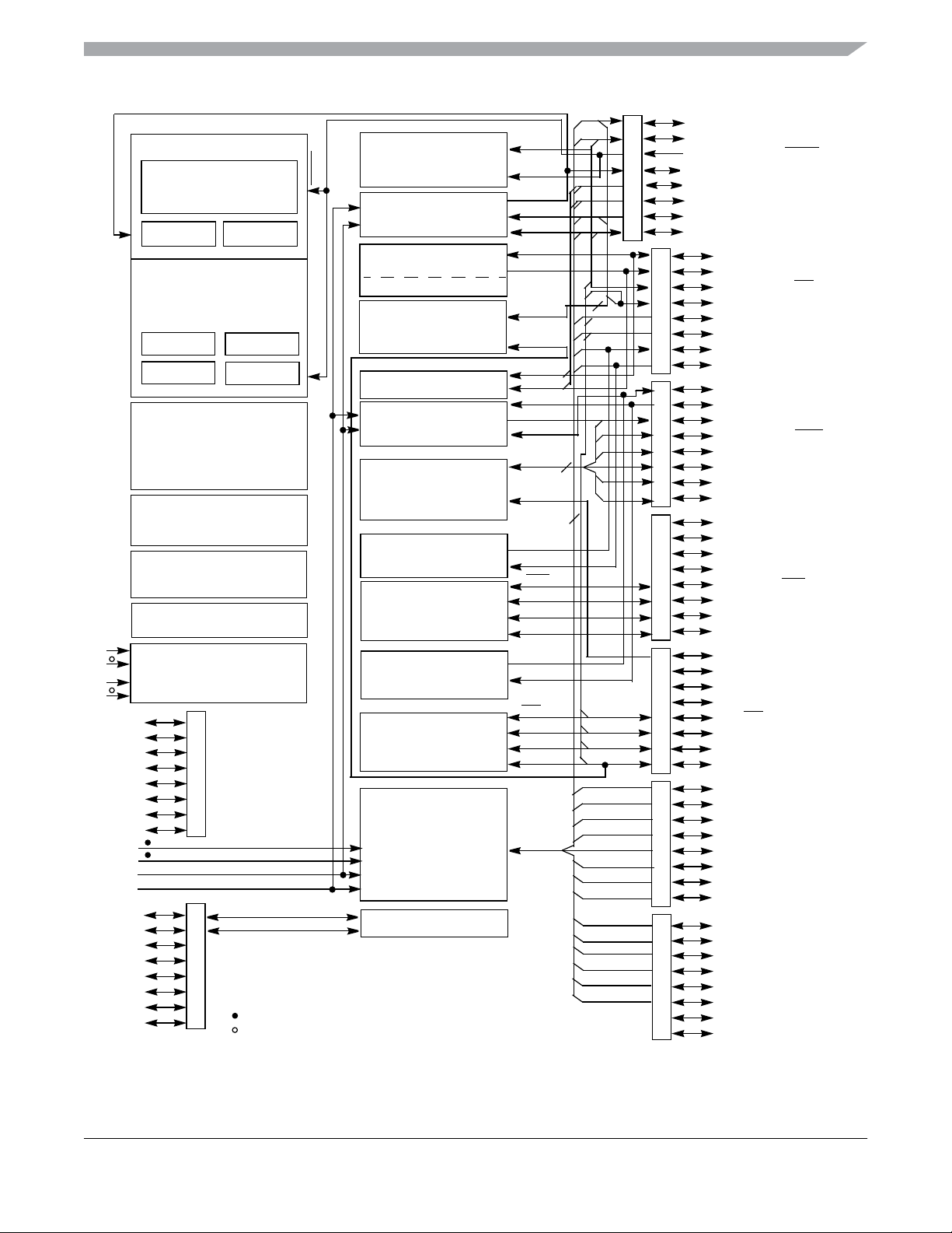
The block diagram in Figure 1-1 shows the structure of the MC9S08QE128 Series MCU.
MC9S08QE128 MCU Series Reference Manual, Rev. 2
20 Freescale Semiconductor
Page 20
BKGD/MS
+
V
DD
V
DD
V
SS
V
SS
PTJ7
PTJ6
PTJ5
PTJ4
PTJ3
PTJ2
PTJ1
PTJ0
V
REFH
V
REFL
V
DDA
V
SSA
PTH7/SDA2
PTH6/SCL2
PTH5
PTH4
PTH3
PTH2
PTH1
PTH0
HCS08 CORE
CPU
BDC
BKP
HCS08 SYSTEM CONTROL
RESETS AND INTERRUPTS
MODES OF OPERATION
POWER MANAGEMENT
COP
INT
LVD
IRQ
USER FLASH
128K / 96K / 64K
USER RAM
8K / 6K / 4K
DEBUG MODULE (DBG)
REAL TIME COUNTER (RTC)
VOLT AGE
REGULATOR
PORT J
PORT H
- V
REFH/VREFL
- V
DD
TPM1CH2-
TPM1CH0
TPM1CLK
ACMP1O
ACMP1+
ACMP1-
EXTAL
XTAL
RESET
RESET
3-CHANNEL TIMER/PWM
MODULE (TPM1)
ANALOG COMPARATOR
(ACMP1)
INTERNAL CLOCK
SOURCE (ICS)
OSCILLATOR (XOSC)
3-CHANNEL TIMER/PWM
MODULE (TPM2)
IRQ
IIC MODULE (IIC1)
TPM2CH2TPM2CH0
TPM2CLK
SCL1
SDA1
ACMP2+
ANALOG COMPARATOR
(ACMP2)
ACMP2O
ACMP2-
TPM3CH5 -
6-CHANNEL TIMER/PWM
MODULE (TPM3)
TPM3CH0
TPM3CLK
6
10
SERIAL COMMUNICATIONS
INTERFACE (SCI1)
TxD1
RxD1
SS2
SERIAL PERIPHERAL
INTERFACE MODULE (SPI2)
SERIAL COMMUNICATIONS
INTERFACE (SCI2)
MISO2
MOSI2
SPSCK2
TxD2
RxD2
SS1
SERIAL PERIPHERAL
INTERFACE MODULE (SPI1)
MISO1
MOSI1
SPSCK1
24-CHANNEL,12-BIT
ANALOG-TO-DIGITAL
CONVERTER (ADC)
SDA2
SCL2
internally connected to V
and VSS pins are each internally connected to two pads in 32-pin package
IIC MODULE (IIC2)
in 48-pin and 32-pin packages
DDA/VSSA
Chapter 1 Device Overview
PTA7/TPM2CH2/ADP9
PTA6/TPM1CH2/ADP8
PTA5/IRQ/TPM1CLK/
RESET
PTA4/ACMP1O/BKGD/MS
PORT A
PTA3/KBI1P3/SCL1/ADP3
PTA2/KBI1P2/SDA1/ADP2
PTA1/KBI1P1/TPM2CH0/ADP1/ACMP1
PTA0/KBI1P0/TPM1CH0/ADP0/ACMP1
PTB7/SCL1/EXTAL
PTB6/SDA1/XTAL
3
PORT B
PTB4/TPM2CH1/MISO1
PTB3/KBI1P7/MOSI1/ADP7
PTB2/KBI1P6/SPSCK1/ADP6
PTB5/TPM1CH1/
SS1
PTB1/KBI1P5/TxD1/ADP5
PTB0/KBI1P4/RxD1/ADP4
PTC7/TxD2/ACMP2-
RSTO
PORT C
PTC6/RxD2/ACMP2+
PTC5/TPM3CH5/ACMP2O
PTC4/TPM3CH4/
PTC3/TPM3CH3
PTC2/TPM3CH2
PTC1/TPM3CH1
PTC0/TPM3CH0
PTD7/KBI2P7
PTD6/KBI2P6
PTD5/KBI2P5
PTD4/KBI2P4
PORT D
PTD3/KBI2P3/SS2
PTD2/KBI2P2/MISO2
PTD1/KBI2P1/MOSI2
PTD0/KBI2P0/SPSCK2
PTE7/TPM3CLK
PTE6
PTE5
PTE4
PORT E
PTE3/SS1
PTE2/MISO1
PTE1/MOSI1
PTE0/TPM2CLK/SPSCK1
PTF7/ADP17
PTF6/ADP16
PTF5/ADP15
PTF4/ADP14
PORT F
PTF3/ADP13
PTF2/ADP12
PTF1/ADP11
PTF0/ADP10
PTG7/ADP23
PTG6/ADP22
PTG5/ADP21
PTG4/ADP20
PORT G
PTG3/ADP19
PTG2/ADP18
PTG1
PTG0
Figure 1-1. MC9S08QE128 Series Block Diagram
MC9S08QE128 MCU Series Reference Manual, Rev. 2
Freescale Semiconductor 21
Page 21

Chapter 1 Device Overview
Table 1-2 provides the functional version of the on-chip modules.
Table 1-2. Module Versions
Module Version
Very Low Power Analog Comparator (ACMPVLP) 1
12-bit Analog-to-Digital Converter (ADC12) 1
Central Processor Unit (CPU) 4
General-Purpose I/O (GPIO) 2
Inter-Integrated Circuit (IIC) 2
Internal Clock Source (ICS) 3
Keyboard Interrupt (KBI) 2
Low Power Oscillator (XOSCVLP) 1
On-Chip In-Circuit Debug/Emulator (DBG) 3
Port Set/Clear (PSC) 1
Real-Time Counter (RTC) 1
Serial Communications Interface (SCI) 4
Serial Peripheral Interface (SPI) 3
Timer Pulse Width Modulator (TPM) 3
MC9S08QE128 MCU Series Reference Manual, Rev. 2
22 Freescale Semiconductor
Page 22

Chapter 1 Device Overview
1.3 System Clock Distribution
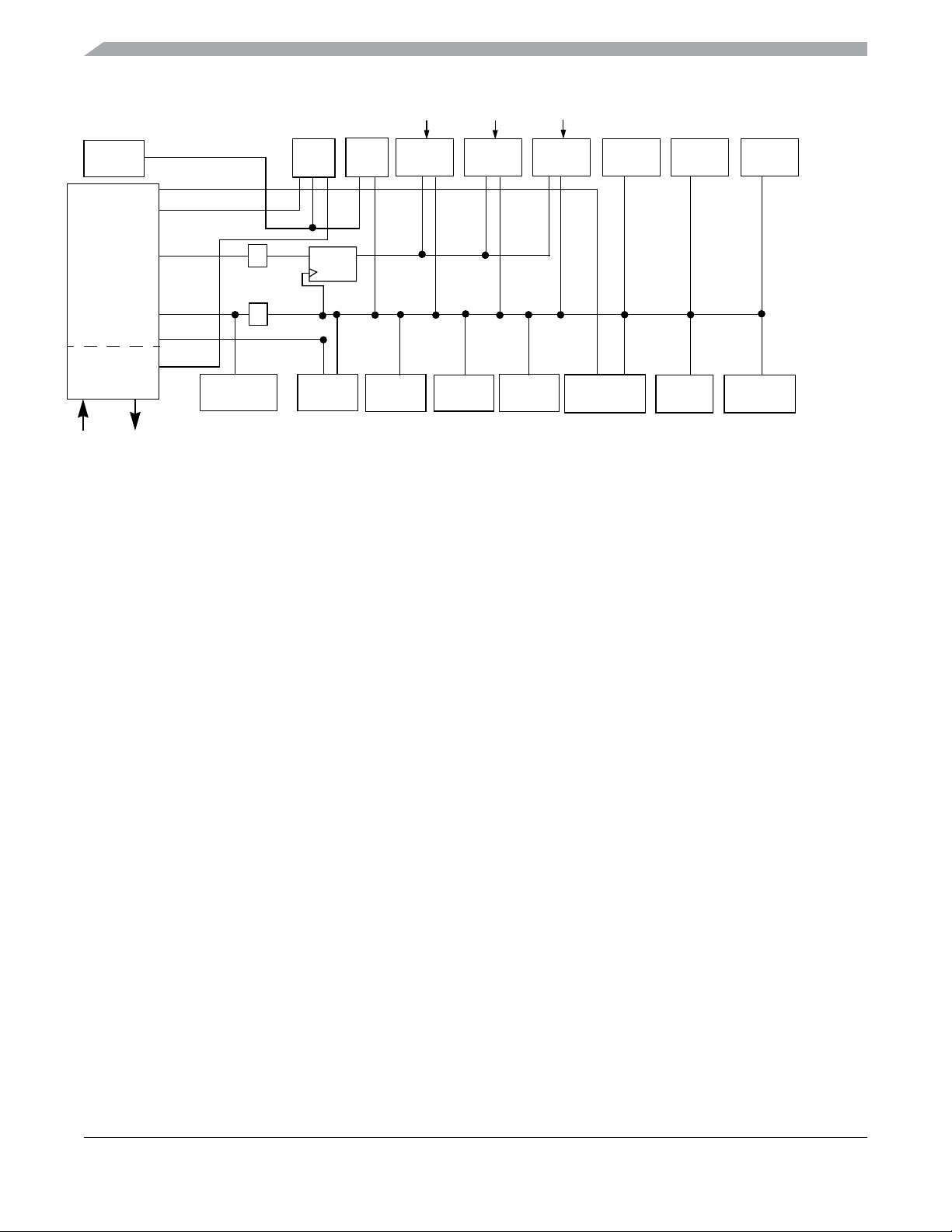
Figure 1-2 shows a simplified clock connection diagram. Some modules in the MCU haveselectable clock
inputs as shown. The clock inputs to the modules indicate the clock(s) that are used to drive the module
function. All memory mapped registers associated with the modules are clocked with BUSCLK. The ICS
supplies the clock sources:
• ICSOUT — This clock source is used as the CPU clock and is divided by 2 to generate the
peripheral bus clock. Control bits in the ICS control registers determine which of three clock
sources is connected:
— Internal reference clock
— External reference clock
— Frequency-locked loop (FLL) output
See Chapter 11, “Internal Clock Source (S08ICSV3)” for details on configuring the ICSOUT
clock.
• ICSLCLK — This clock source is derived from the digitally controlled oscillator (DCO)of the ICS
when the ICS is configured to run off of the internal or external reference clock. Development tools
canselect this internalself-clocked source (~ 8 MHz) tospeed up BDC communications in systems
where the bus clock is slow. See Chapter 11, “Internal Clock Source (S08ICSV3)” for details.
• ICSERCLK — This is the external reference clock and can be selected as the alternate clock for
the ADC module. The Optional External Reference Clock section in Chapter 11, “Internal Clock
Source (S08ICSV3)” explains the ICSERCLK in more detail. See Chapter 10, “Analog-to-Digital
Converter (S08ADC12V1)” for more information regarding the use of ICSERCLK with these
modules.
• ICSIRCLK— This isthe internal reference clock and can be selectedas the real-timecounter clock
source. The Internal Reference Clock section in Chapter 11, “Internal Clock Source (S08ICSV3)
explains the ICSERCLK in more detail. See Chapter 13, “Real-Time Counter (S08RTCV1)” for
more information regarding the use of ICSIRCLK.
• ICSFFCLK — This generates the fixed frequency clock (FFCLK) after being synchronized to the
bus clock. It can be selected as clock source for the TPM modules. The frequency of the
ICSFFCLK is determined by the settings of the ICS. See the Fixed Frequency Clock section in
Chapter 11, “Internal Clock Source (S08ICSV3)” for details.
• LPOCLK — This clock is generated from an internal low power oscillator that is completely
independent of the ICS module. The LPOCLK can be selected as the clock source to the RTC or
COP modules. See Chapter 13, “Real-Time Counter (S08RTCV1)” and Section 5.4, “Computer
Operating Properly (COP) Watchdog” for details on using the LPOCLK with these modules.
• OSCOUT — This is the direct output of the external oscillator module and can be selected as the
real-time counter clock source. See Chapter 13, “Real-Time Counter (S08RTCV1)” for details.
• TPMxCLK — TPMxCLKs are optional external clock sources for the TPM modules. The
TPMxCLK must be limited to 1/4th the frequency of the bus clock for synchronization. See the
External TPM Clock Sources section in Chapter 16, “Timer/Pulse-Width Modulator (S08TPMV3)
for more details.
MC9S08QE128 MCU Series Reference Manual, Rev. 2
Freescale Semiconductor 23
Page 23
Chapter 1 Device Overview
E
TPM2CLK
1 kHZ
LPO
ICS
XOSC
XTAL XTAL
LPOCLK
ICSERCLK
ICSIRCLK
ICSFFCLK
ICSOUT
ICSLCLK
OSCOUT
÷2
÷2
CPU
* The fixed frequency clock (FFCLK) is internally
synchronizedto the bus clockand must not exceedonehalf
of the bus clock frequency.
RTC
BUSCLK
COP
SYNC*
BDC
Figure 1-2. System Clock Distribution Diagram
TPM1CLK
TPM1 TPM2 TPM3 SCI1 SCI2
FFCLK*
DBG
IIC1
IIC2
TPM3CLK
ADC
ADC has min and max
frequency requirements.
See the ADC chapter
and data sheet for
details.
SPI1
FLASH SPI2
Flash has frequency
requirementsforprogram
and erase operation. See
the data sheet for details.
MC9S08QE128 MCU Series Reference Manual, Rev. 2
24 Freescale Semiconductor
Page 24

Chapter 2 Pins and Connections
This section describes signals that connect to package pins. It includes pinout diagrams, recommended
system connections, and detailed discussions of signals.
2.1 Device Pin Assignment
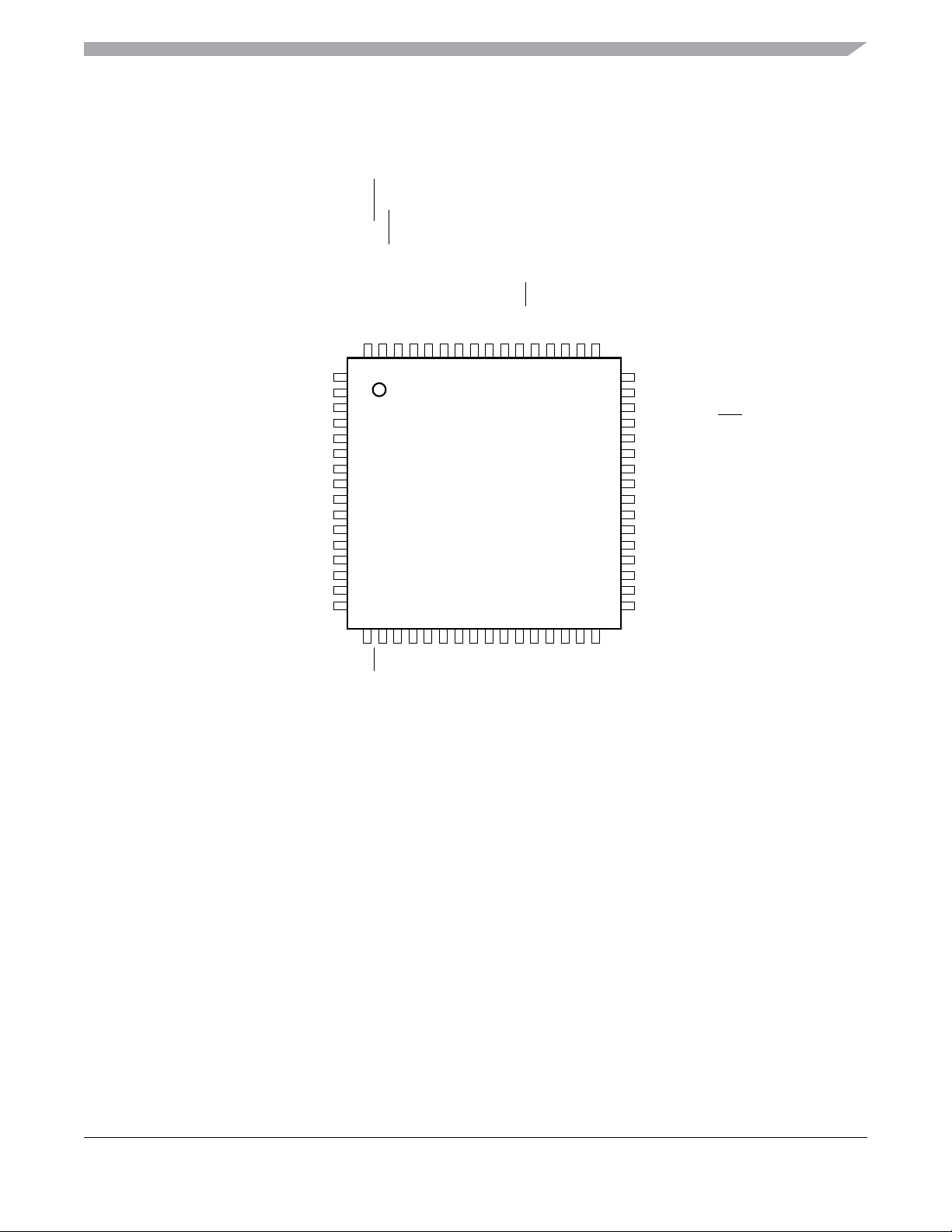
This section shows the pin assignments for MC9S08QE128 Series devices in the available packages.
MC9S08QE128 MCU Series Reference Manual, Rev. 2
Freescale Semiconductor 25
Page 25

Chapter 2 Pins and Connections
RESET
RSTO
PTE1/MOSI1
PTA4/ACMP1O/BKGD/MS
PTE0/TPM2CLK/SPSCK1
PTG1
PTG2/ADP18
PTC4/TPM3CH4/
PTC5/TPM3CH5/ACMP2O
PTA5/IRQ/TPM1CLK/
PTG0
SS1
PTG3/ADP19
PTE2/MISO1
PTG5/ADP21
PTE3/
PTG4/ADP20
PTG7/ADP23
PTC6/RxD2/ACMP2+
PTG6/ADP22
PTA1/KBI1P1/TPM2CH0/ADP1/ACMP1
PTA1/KBI1P1/TPM2CH0/AD
PTC7/TxD2/ACMP2-
PTA0/KBI1P0/TPM1CH0/ADP0/ACMP1
PTD1/KBI2P1/MOSI2
PTD0/KBI2P0/SPSCK2
PTH7/SDA2
PTH6/SCL2
PTH5
PTH4
PTE7/TPM3CLK
V
DD
V
DDAD
V
REFH
V
REFL
V
SSAD
V
SS
PTB7/SCL1/EXTAL
PTB6/SDA1/XTAL
PTH3
PTH2
PTH1
PTH0
PTE6
80797877767574737271706968676665646362
1
2
3
4
5
6
7
8
9
10
11
12
13
14
15
16
17
18
19
20
21222324252627282930313233343536373839
PTE5
PTD7/KBI2P7
PTD6/KBI2P6
PTC3/TPM3CH3
PTD5/KBI2P5
PTC2/TPM3CH2
PTJ6
PTJ7
PTJ4
PTJ5
PTC0/TPM3CH0
PTC1/TPM3CH1
PTF6/ADP16
PTF7/ADP17
PTB5/TPM1CH1/SS1
PTB4/TPM2CH1/MISO1
61
60
PTA2/KBI1P2/SDA1/ADP2
59
PTA3/KBI1P3/SCL1/ADP3
58
PTD2/KBI2P2/MISO2
57
PTD3/KBI2P3/
56
PTD4/KBI2P4
55
PTJ0
54
PTJ1
53
PTF0/ADP10
52
PTF1/ADP11
51
V
SS
50
V
DD
49
PTE4
48
PTA6/TPM1CH2/ADP8
47
PTA7/TPM2CH2/ADP9
46
PTF2/ADP12
45
PTF3/ADP13
44
PTJ2
43
PTJ3
42
PTB0/KBI1P4/RxD1/ADP4
41
PTB1/KBI1P5/TxD1/ADP5
40
PTF5/ADP15
PTF4/ADP14
PTB3/KBI1P7/MOSI1/ADP7
PTB2/KBI1P6/SPSCK1/ADP6
SS2
Pins in bold are added from the next smaller package.
Figure 2-1. 80-Pin LQFP
MC9S08QE128 MCU Series Reference Manual, Rev. 2
26 Freescale Semiconductor
Page 26
RESET
1
1
PTE1/MOSI1
PTA4/ACMP1O/BKGD/MS
PTE0/TPM2CLK/SPSCK1
PTG1
PTG2/ADP18
PTC4/TPM3CH4/RSTO
PTA5/IRQ/TPM1CLK/
PTG0
PTC5/TPM3CH5/ACMP2O
SS1
PTG3/ADP19
PTE2/MISO1
PTC6/RxD2/ACMP2+
PTE3/
PTC7/TxD2/ACMP2-
Chapter 2 Pins and Connections
PTA1/KBI1P1/TPM2CH0/ADP1/ACMP
PTA0/KBI1P0/TPM1CH0/ADP0/ACMP
PTD1/KBI2P1/MOSI2
PTD0/KBI2P0/SPSCK2
PTH7/SDA2
PTH6/SCL2
PTE7/TPM3CLK
V
DD
V
DDAD
V
REFH
V
REFL
V
SSAD
V
SS
PTB7/SCL1/EXTAL
PTB6/SDA1/XTAL
PTH1
PTH0
PTE6
Pins in bold are added from the next smaller package.
646362616059585756555453525150
1
2
3
4
5
6
7
8
9
10
11
12
13
14
15
16
171819202122232425262728293031
PTE5
PTF6/ADP16
PTD7/KBI2P7
PTD6/KBI2P6
PTC3/TPM3CH3
PTC2/TPM3CH2
PTF7/ADP17
PTD5/KBI2P5
PTC0/TPM3CH0
PTC1/TPM3CH1
PTB5/TPM1CH1/SS1
PTB4/TPM2CH1/MISO1
49
PTA2/KBI1P2/SDA11/ADP2
48
PTA3/KBI1P3/SCL1/ADP3
47
PTD2/KBI2P2/MISO2
46
PTD3/KBI2P3/
45
PTD4/KBI2P4
44
PTF0/ADP10
43
PTF1/ADP11
42
V
41
SS
V
40
DD
PTE4
39
PTA6/TPM1CH2/ADP8
38
PTA7/TPM2CH2/ADP9
37
PTF2/ADP12
36
PTF3/ADP13
35
PTB0/KBI1P4/RxD1/ADP4
34
PTB1/KBI1P5/TxD1/ADP5
33
32
PTF5/ADP15
PTF4/ADP14
PTB3/KBI1P7/MOSI1/ADP7
PTB2/KBI1P6/SPSCK1/ADP6
SS2
Figure 2-2. 64-Pin LQFP
MC9S08QE128 MCU Series Reference Manual, Rev. 2
Freescale Semiconductor 27
Page 27

Chapter 2 Pins and Connections
P1
P1
PTD1/KBI2P1/MOSI2
PTD0/KBI2P0/SPSCK2
PTE7/TPM3CLK
V
DDAD
V
V
V
PTB7/SCL1/EXTAL
PTB6/SDA11/XTAL
PTE6
V
DD
REFH
REFL
SSAD
V
SS
RSTO
PTA5/IRQ/TPM1CLK/RESET
PTC4/TPM3CH4/
PTA4/ACMP1O/BKGD/MS
48
47
PTC5/TPM3CH5/ACMP2O
46
45
1
2
3
4
5
6
7
8
9
10
11
12
14
15
13
16
PTE1/MOSI1
PTE0/TPM2CLK/SPSCK1
44
43
17
18
PTE2/MISO1
42
19
SS1
PTE3/
PTC6/RxD2/ACMP2+
PTC7/TxD2/ACMP2-
41
40
39
20
21
22
PTA1/KBI1P1/TPM2CH0/AD
PTA1/KBI1P1/TPM2CH0/ADP1/ACM
PTA0/KBI1P0/TPM1CH0/ADP0/ACM
37
38
23
PTA2/KBI1P2/SDA1/ADP2
36
PTA3/KBI1P3/SCL1/ADP3
35
PTD2/KBI2P2/MISO2
34
PTD3/KBI2P3/
33
PTD4/KBI2P4
32
V
31
SS
V
30
DD
PTE4
29
PTA6/TPM1CH2/ADP8
28
PTA7/TPM2CH2/ADP9
27
PTB0/KBI1P4/RxD1/ADP4
26
PTB1/KBI1P5/TxD1/ADP5
25
SS2
24
SS1
PTE5
PTD7/KBI2P7
PTD6/KBI2P6
PTC3/TPM3CH3
PTC2/TPM3CH2
PTD5/KBI2P5
PTC0/TPM3CH0
PTC1/TPM3CH1
PTB5/TPM1CH1/
PTB4/TPM2CH1/MISO1
PTB3/KBI1P7/MOSI1/ADP7
PTB2/KBI1P6/SPSCK1/ADP6
Pins in bold are added from the next smaller package.
Figure 2-3. 48-Pin QFN
MC9S08QE128 MCU Series Reference Manual, Rev. 2
28 Freescale Semiconductor
Page 28

P1
P1
5
4
2
3
PTD1/KBI2P1/MOSI2
PTD0/KBI2P0/SPSCK2
PTE7/TPM3CLK
V
DD
V
DDAD
V
REFH
V
REFL
V
SSAD
V
PTB7/SCL1/EXTAL
PTB6/SDA1/XTAL
SS
RESET
PTA5/IRQ/TPM1CLK/
PTA4/ACMP1O/BKGD/MS
43
44
1
2
3
4
5
6
7
8
9
10
11
13
12
PTC4/TPM3CH4/RSTO
PTC5/TPM3CH5/ACMP2O
42
41
14
15
PTE1
PTE0/TPM2CLK
40
39
16
17
PTE2
PTC6/RxD2/ACMP2+
PTC7/TxD2/ACMP2-
38
37
36
18
19
20
Chapter 2 Pins and Connections
PTA0/KBI1P0/TPM1CH0/ADP0/ACM
PTA1/KBI1P1/TPM2CH0/ADP1/ACM
35
34
PTA2/KBI1P2/SDA1/ADP
33
PTA3/KBI1P3/SCL1/ADP
32
PTD2/KBI2P2/MISO2
31
PTD3/KBI2P3/SS2
30
PTD4/KBI2P4
29
V
28
SS
V
27
DD
PTA6/TPM1CH2/ADP8
26
PTA7/TPM2CH2/ADP9
25
PTB0/KBI1P4/RxD1/ADP
24
PTB1/KBI1P5/TxD1/ADP
23
22
21
PTD7/KBI2P7
PTD6/KBI2P6
PTC3/TPM3CH3
PTC2/TPM3CH2
PTD5/KBI2P5
PTC0/TPM3CH0
PTC1/TPM3CH1
PTB5/TPM1CH1/SS1
PTB4/TPM2CH1/MISO1
PTB3/KBI1P7/MOSI1/ADP7
PTB2/KBI1P6/SPSCK1/ADP6
Pins in bold are added from the next smaller package.
Figure 2-4. 44-Pin QFP
MC9S08QE128 MCU Series Reference Manual, Rev. 2
Freescale Semiconductor 29
Page 29
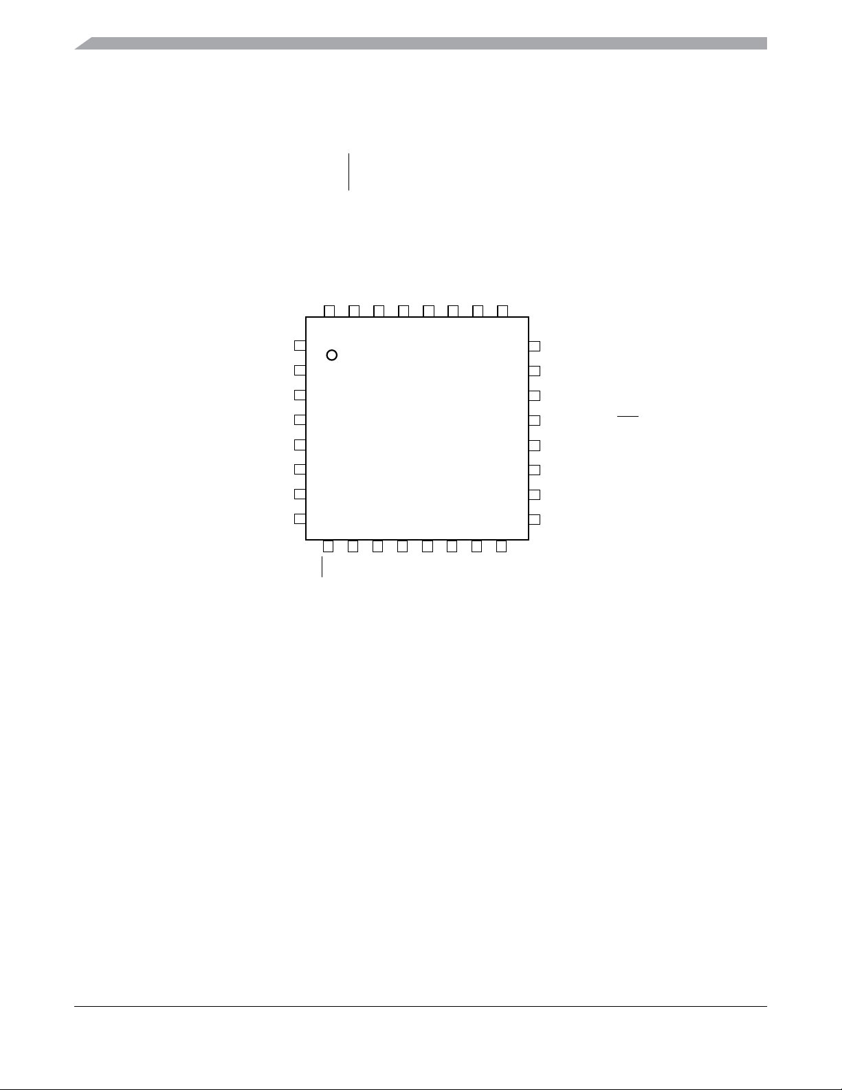
Chapter 2 Pins and Connections
PTC4/TPM3CH4/RSTO
PTA5/IRQ/TPM1CLK/RESET
PTA4/ACMP1O/BKGD/MS
PTC6/RxD2/ACMP2+
PTC5/TPM3CH5/ACMP2O
PTA1/KBIP1/TPM2CH0/ADP1/ACMP1-
PTA0/KBIP0/TPM1CH0/ADP0/ACMP1+
PTC7/TxD2/ACMP2-
PTD1/KBI2P1/MOSI2
PTD0/KBI2P0/SPSCK2
V
DD
V
REFH/VDDAD
V
REFL/VSSAD
V
SS
PTB7/SCL1/EXTAL
PTB6/SDA1/XTAL
31 30 29 28
32
1
2
3
4
5
6
7
8
9
10
PTB5/TPM1CH1/SS1
11
12 13 14
PTC3/TPM3CH3
PTC2/TPM3CH2
PTC1/TPM3CH1
PTC0/TPM3CH0
PTB4/TPM2CH1/MISO1
252627
PTA2/KBIP2/SDA1/ADP2
24
PTA3/KBIP3/SCL1/ADP3
23
22
PTD2/KBI2P2/MISO2
21
PTD3/KBI2P3/SS2
20
PTA6/TPM1CH2/ADP8
19
PTA7/TPM2CH2/ADP9
18
PTB0/KBI1P4/RxD1/ADP4
17
15
16
PTB3/KBI1P7/MOSI1/ADP7
PTB2/KBI1P6/SPSCK1/ADP6
PTB1/KBI1P5/TxD1/ADP5
Figure 2-5. 32-Pin LQFP
MC9S08QE128 MCU Series Reference Manual, Rev. 2
30 Freescale Semiconductor
Page 30

Chapter 2 Pins and Connections
2.2 Recommended System Connections
Figure 2-6 shows pin connections that are common to MC9S08QE128 Series application systems.
MC9S08QE128 MCU Series Reference Manual, Rev. 2
Freescale Semiconductor 31
Page 31
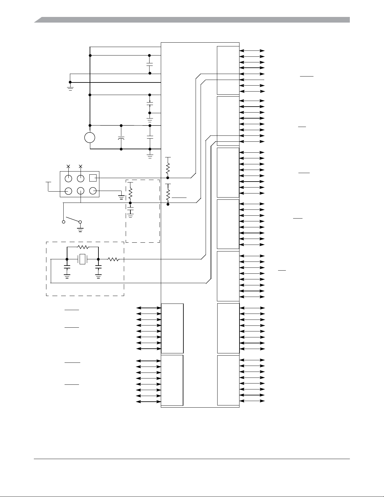
Chapter 2 Pins and Connections
+
-
SYSTEM
POWER
+
3 V
BACKGROUND HEADER
V
DD
OPTIONAL
MANUAL
RESET
(NOTE 1)
R
F
C1
X1
OPTIONAL EXTERNAL OSCILLATOR
(NOTE 4)
NOTES:
1. RESET pin can only
be used to reset into
user mode, you can
not enter BDM using
RESET pin. BDM
can be entered by
holding MS low
during POR or
writing a 1 to BDFR
in SBDFR with MS
low after issuing
BDM command.
2. RESET/IRQfeatures
have optional
internal pullup
device.
3. RC filter on
RESET/IRQ pin
recommended for
noisy environments.
4. C1, C2, RF, and R
are not required
when low range low
power oscillator is
selected.
S
C
10 μF
C2
BLK
+
R
S
PTH0
PTH1
PTH2
PTH3
PTH4
PTH5
PTH6/SCL2
PTH7/SDA2
C
BYAD
0.1 μF
C
BY
0.1 μF
C
BY
0.1 μF
V
DD
4.7 kΩ–10 kΩ
0.1 μF
OPTIONAL
EMC
PROTECTION
(NOTE 3)
PTJ0
PTJ1
PTJ2
PTJ3
PTJ4
PTJ5
PTJ6
PTJ7
V
DDA
V
REFH
V
REFL
V
SSA
V
DD
V
SS
V
DD
V
SS
BKGD/MS
RESET/IRQ
(NOTE 2)
XTAL
EXTAL
PORT
J
PORT
H
MC9S08QE128
PORT
A
PORT
B
PORT
C
PORT
D
PORT
E
PORT
F
PORT
G
PTA0/KBI1P0/TPM1CH0/ADP0/ACMP1
PTA1/KBI1P1/TPM2CH0/ADP1/ACMP1
PTA2/KBI1P2/SDA1/ADP2
PTA3/KBI1P3/SCL1/ADP3
PTA4/ACMP1O/BKGD/MS
PTA5/IRQ/TCLK1/
RESET
PTA6/TPM1CH2/ADP8
PTA7/TPM2CH2/ADP9
PTB0/KBI1P4/RxD1/ADP4
PTB1/KBI1P5/TxD1/ADP5
PTB2/KBI1P6/SPSCK1/ADP6
PTB3/KBI1P7/MOSI1/ADP7
PTB4/TPM2CH1/MISO1
PTB5/TPM1CH1/SS1
PTB6/SDA1/XTAL
PTB7/SCL1/EXTAL
PTC0/TPM3CH0
PTC1/TPM3CH1
PTC2/TPM3CH2
PTC3/TPM3CH3
PTC4/TPM3CH4/
RSTO
PTC5/TPM3CH5/ACMP2O
PTC6/RxD2/ACMP2+
PTC7/TxD2/ACMP2-
PTD0/KBI2P0/SPSCK2
PTD1/KBI2P1/MOSI2
PTD2/KBI2P2/MISO2
PTD3/KBI2P3/
SS2
PTD4/KBI2P4
PTD5/KBI2P5
PTD6/KBI2P6
PTD7/KBI2P7
PTE0/TCLK2/SPSCK1
PTE1/MOSI1
PTE2/MISO1
PTE3/SS1
PTE4
PTE5
PTE6
PTE7/TPM3CLK
PTF0/ADP10
PTF1/ADP11
PTF2/ADP12
PTF3/ADP13
PTF4/ADP14
PTF5/ADP15
PTF6/ADP16
PTF7/ADP17
PTG0
PTG1
PTG2/ADP18
PTG3/ADP19
PTG4/ADP20
PTG5/ADP21
PTG6/ADP22
PTG7/ADP23
Figure 2-6. Basic System Connections
MC9S08QE128 MCU Series Reference Manual, Rev. 2
32 Freescale Semiconductor
Page 32

Chapter 2 Pins and Connections
2.2.1 Power
VDD and VSS are the primary power supply pins for the MCU. This voltage source supplies power to all
I/O buffer circuitry and to an internal voltage regulator. The internal voltage regulator provides regulated
lower-voltage source to the CPU and other internal circuitry of the MCU.
Typically, application systems have two separate capacitors across the power pins. In this case, there
should be a bulk electrolytic capacitor, such as a 10-μF tantalum capacitor,to provide bulk charge storage
for the overall system and a 0.1-μF ceramic bypass capacitor located as near to the MCU power pins as
practical to suppress high-frequency noise. Actual decoupling capacitor values and number will vary
according to layout and application. The MC9S08QE128 Series has two V
package. Each pin must have a bypass capacitor for best noise suppression.
pins except on the 32-pin
DD
V
DDA
and V
are the analog power supply pins for the MCU. This voltage source supplies power to the
SSA
ADC module. A 0.1-μF ceramic bypass capacitor should be located as near to the MCU power pins as
practical to suppress high-frequency noise.
2.2.2 Oscillator
Immediately after reset, the MCU uses an internally generated clock provided by the internal clock source
(ICS) module. For more information on the ICS, see Chapter 11, “Internal Clock Source (S08ICSV3).”
The oscillator (XOSCVLP) in this MCU is a Pierce oscillator that can accommodate a crystal or ceramic
resonator. Optionally, an external clock source can be connected to the EXTAL input pin. The oscillator
can be configured to run in stop2 or stop3 modes.
Refer to Figure 2-6 for the following discussion. R
resistors such as carbon composition resistors. Wire-wound resistors, and some metal film resistors, have
too much inductance. C1 and C2 normally should be high-quality ceramic capacitors that are specifically
designed for high-frequency applications.
is used to provide a bias path to keepthe EXTAL input in its linear range during crystal startup; its value
R
F
is not generally critical. Typicalsystems use 1 MΩ to 10 MΩ.Higher values are sensitive to humidity and
lower values reduce gain and (in extreme cases) could prevent startup.
C1 and C2 are typically in the 5-pF to 25-pF range and are chosen to match the requirements of a specific
crystal or resonator. Be sure to take into account printed circuit board (PCB) capacitance and MCU pin
capacitance when selecting C1 and C2. The crystal manufacturer typically specifies a load capacitance
which is the series combination of C1 and C2 (which are usually the same size). As a first-order
approximation, use 10 pF as an estimate of combined pin and PCB capacitance for each oscillator pin
(EXTAL and XTAL).
(when used) and RF should be low-inductance
S
When using the oscillator in low range and low gain mode, the external components R
S,RF,C1
and C2are
not required.
2.2.3 RESET and RSTO
After a power-on reset (POR), the PTA5/IRQ/TCLK/RESET pin defaults to a general-purpose input port
pin, PTA5. Setting RSTPE in SOPT1 configures the pin to be the
MC9S08QE128 MCU Series Reference Manual, Rev. 2
Freescale Semiconductor 33
RESET pin. After configured as RESET,
Page 33

Chapter 2 Pins and Connections
the pin will remain RESET until the next POR. The RESET pin can be used to reset the MCU from an
external source when the pin is driven low. When enabled as the
RESET pin (RSTPE = 1), the pin is
configured as an input only with an internal pullup device automatically enabled.
NOTE
This pin does not contain a clamp diode to V
above V
DD
.
and should not be driven
DD
NOTE
RESET pin is pulled to VDDinternally. The external voltage measured
The
on the
RESET pin will be less than VDD. Therefore, the RESET pullup
should not be used to pullup components external to the MCU.
NOTE
In EMC-sensitiveapplications, an external RC filter is recommended on the
RESET pin, if enabled. See Figure 2-6 for an example.
After a power-on reset (POR), the PTC4/TPM3CH4/RSTO pin defaults to a general-purpose port pin,
PTC4. Setting RSTOPE in SOPT1 configures the pin to be the
pin will remain
RSTO until the next POR. The RSTO pin will reflect the current state of the internal MCU
reset signal. As long as the MCU is not in a reset state, the
RSTO pin. After configured as RSTO, the
RSTO pin will drive high. Whenever the MCU
is in a reset state, this pin will drive low until the internal reset signal is released. When enabled as the
RSTO pin (RSTOPE = 1), the pin is automatically configured as an output only. The RSTO pin can be
enabled independently of the
RESET pin.
2.2.4 Background / Mode Select (BKGD/MS)
During a power-on-reset (POR) or background debug force reset (see Section 5.8.3, “System Background
Debug Force Reset Register (SBDFR),” for more information), the PTA4/ACMPO/BKGD/MS pin
functions as a mode select pin. Immediately after any reset, the pin functions as the background pin and
can be used for background debug communication. When enabled as the BKGD/MS pin (BKGDPE = 1),
an internal pullup device is automatically enabled.
The background debug communication function is enabled when BKGDPE in SOPT1 is set. BKGDPE is
set following any reset of the MCU and must be cleared to use the PTA4/ACMPO/BKGD/MS pin’s
alternative pin functions.
If nothing is connected to this pin, the MCU will enter normal operating mode at the rising edge of the
internal reset after a POR or force BDC reset. If a debug system is connected to the 6-pin standard
background debug header, it can hold BKGD/MS low during a POR or immediately after issuing a background debug force reset, which will force the MCU to active background mode.
The BKGD/MS pin is used primarily for background debug controller (BDC) communications using a
custom protocol that uses 16 clock cycles of the target MCU’sBDC clock per bit time. The target MCU’s
BDC clock could be as fast as the bus clock rate, so there should never be any significant capacitance
connected to the BKGD/MS pin that could interfere with background serial communications.
MC9S08QE128 MCU Series Reference Manual, Rev. 2
34 Freescale Semiconductor
Page 34

Chapter 2 Pins and Connections
Although the BKGD/MS pin is a pseudo open-drain pin, the background debug communication protocol
provides brief, actively driven, high speedup pulses to ensure fast rise times. Small capacitances from
cables and the absolute value of the internal pull-up device play almost no role in determining rise and fall
times on the BKGD/MS pin.
2.2.5 ADC Reference Pins (V
The V
REFH
and V
pins are the voltage reference high and voltage reference low inputs, respectively,
REFL
REFH
for the ADC module. In the 32-pin package, V
REFH
, V
and V
REFL
)
are shared with V
REFL
DDA
and V
SSA
,
respectively.
2.2.6 General-Purpose I/O and Peripheral Ports
The MC9S08QE128 Series of MCUs support up to 70 general-purpose I/O pins 1 input-only pin, and 1
output-only pin, which are shared with on-chip peripheral functions (timers, serial I/O, ADC, ACMP, etc.).
When a port pin is configured as a general-purpose output or a peripheral uses the port pin as an output,
software can select one of two drive strengths and enable or disable slew rate control. When a port pin is
configured as a general-purpose input or a peripheral uses the port pin as an input, software can enable a
pull-updevice. Immediately after reset, all of thesepins are configuredas high-impedance general-purpose
inputs with internal pull-up devices disabled.
PTA5 is a special-case input pin. When the PTA5/IRQ/TCLK/
pullup enabled, the voltage observed on the pin will not be pulled to V
on the PTA5 node will be at VDD.
When an on-chip peripheral system is controlling a pin, data direction control bits still determine what is
read from port data registers even though the peripheral module controls the pin direction by controlling
the enable for the pin’s output buffer. For information about controlling these pins as general-purpose I/O
pins, see Chapter 6, “Parallel Input/Output Control.”
RESET pin is configured as PTA5with the
. However, the internal voltage
DD
NOTE
To avoid extra current drain from floating input pins, the reset initialization
routine in the application program should either enable on-chip pull-up
devices or change the direction of unused or non-bonded pins to outputs so
they do not float.
MC9S08QE128 MCU Series Reference Manual, Rev. 2
Freescale Semiconductor 35
Page 35
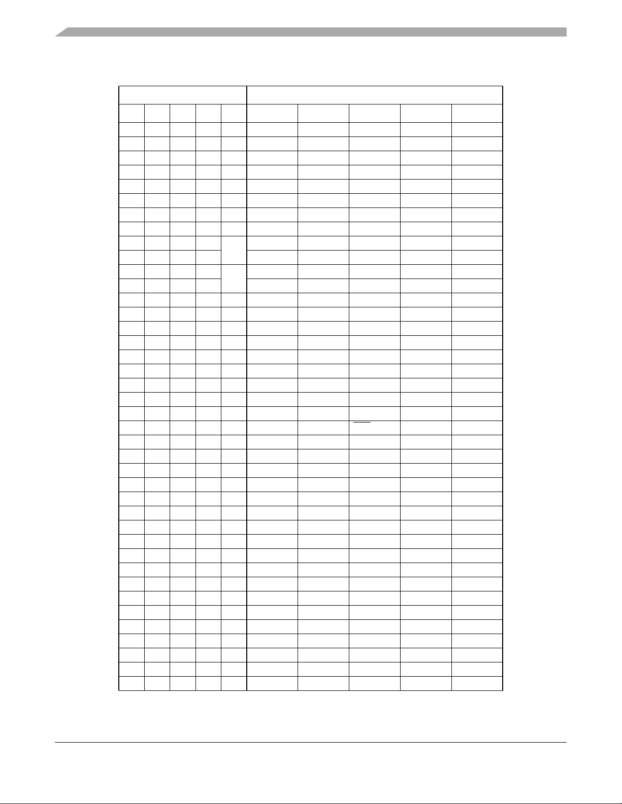
Chapter 2 Pins and Connections
Table 2-1. Pin Assignment by Package and Pin Sharing Priority
Pin Number <-- Lowest Priority --> Highest
80 64 48 44 32 Port Pin Alt 1 Alt 2 Alt 3 Alt 4
11111PTD1 KBI2P1 MOSI2
22222PTD0 KBI2P0 SPSCK2
3 3 — — — PTH7 SDA2
4 4 — — — PTH6 SCL2
5 ————PTH5
6 ————PTH4
7533—PTE7 TPM3CLK
86443 V
9755
10866 V
11977
12 10 8 8 V
13 11 9 9 6 V
14 12 10 10 7 PTB7 SCL1
15 13 11 11 8 PTB6 SDA1
16————PTH3
17————PTH2
18 14 — — — PTH1
19 15 — — — PTH0
20 16 12 — — PTE6
21 17 13 — — PTE5
22 18 14 12 9 PTB5 TPM1CH1
23 19 15 13 10 PTB4 TPM2CH1 MISO1
24 20 16 14 11 PTC3 TPM3CH3
25 21 17 15 12 PTC2 TPM3CH2
26 22 18 16 — PTD7 KBI2P7
27 23 19 17 — PTD6 KBI2P6
28 24 20 18 — PTD5 KBI2P5
29————PTJ7
30————PTJ6
31————PTJ5
32————PTJ4
33 25 21 19 13 PTC1 TPM3CH1
34 26 22 20 14 PTC0 TPM3CH0
35 27 — — — PTF7 ADP17
36 28 — — — PTF6 ADP16
37 29 — — — PTF5 ADP15
38 30 — — — PTF4 ADP14
39 31 23 21 15 PTB3 KBI1P7 MOSI1
40 32 24 22 16 PTB2 KBI1P6 SPSCK1
DD
V
4
5
1
1
2
SS1
2
2
2
DDA
REFH
V
REFL
SSA
SS
EXTAL
XTAL
ADP7
ADP6
MC9S08QE128 MCU Series Reference Manual, Rev. 2
36 Freescale Semiconductor
Page 36
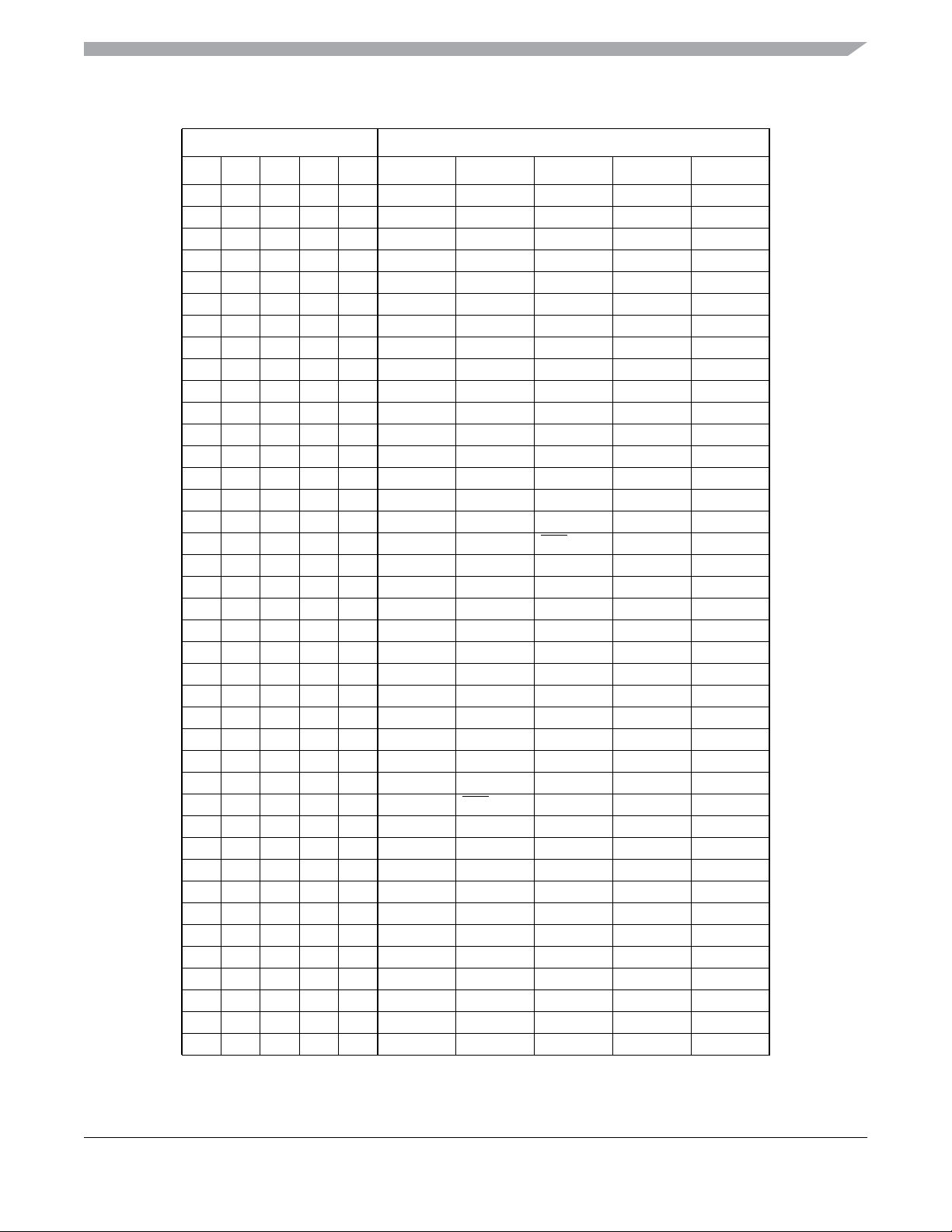
Chapter 2 Pins and Connections
Table 2-1. Pin Assignment by Package and Pin Sharing Priority (continued)
Pin Number <-- Lowest Priority --> Highest
80 64 48 44 32 Port Pin Alt 1 Alt 2 Alt 3 Alt 4
41 33 25 23 17 PTB1 KBI1P5 TxD1 ADP5
42 34 26 24 18 PTB0 KBI1P4 RxD1 ADP4
43————PTJ3
44————PTJ2
45 35 — — — PTF3 ADP13
46 36 — — — PTF2 ADP12
47 37 27 25 19 PTA7 TPM2CH2 ADP9
48 38 28 26 20 PTA6 TPM1CH2 ADP8
49 39 29 — — PTE4
50 40 30 27 — V
51 41 31 28 — V
52 42 — — — PTF1 ADP11
53 43 — — — PTF0 ADP10
54————PTJ1
55————PTJ0
56 44 32 29 — PTD4 KBI2P4
57 45 33 30 21 PTD3 KBI2P3
SS2
58 46 34 31 22 PTD2 KBI2P2 MISO2
59 47 35 32 23 PTA3 KBI1P3 SCL1
60 48 36 33 24 PTA2 KBI1P2 SDA1
61 49 37 34 25 PTA1 KBI1P1 TPM2CH0 ADP1
62 50 38 35 26 PTA0 KBI1P0 TPM1CH0 ADP0
1
1
3
3
63 51 39 36 27 PTC7 TxD2 ACMP264 52 40 37 28 PTC6 RxD2 ACMP2+
65————PTG7 ADP23
66————PTG6 ADP22
67————PTG5 ADP21
68————PTG4 ADP20
2
69 53 41 — — PTE3
70 54 42 38 — PTE2 MISO1
SS1
2
71 55 — — — PTG3 ADP19
72 56 — — — PTG2 ADP18
73 57 — — — PTG1
74 58 — — — PTG0
75 59 43 39 — PTE1 MOSI1
76 60 44 40 — PTE0 TPM2CLK SPSCK1
2
2
77 61 45 41 29 PTC5 TPM3CH5 ACMP2O
78 62 46 42 30 PTC4 TPM3CH4 RSTO
79 63 47 43 31 PTA5 IRQ TPM1CLK RESET
80 64 48 44 32 PTA4 ACMP1O BKGD MS
DD
SS
ADP3
ADP2
ACMP1ACMP1+
3
3
MC9S08QE128 MCU Series Reference Manual, Rev. 2
Freescale Semiconductor 37
Page 37

Chapter 2 Pins and Connections
1
IIC1 pins (SCL1 and SDA1) can be repositioned using IIC1PS in SOPT2. Defaultlocations are
PTA3 and PTA, respectively.
2
SPI1 pins (SS1, MISO1, MOSI1, and SPSCK1) can be repositioned using SPI1PS in SOPT2.
Default locations are PTB5, PTB4, PTB3, and PTB2.
3
If ADC and ACMP1 are enabled, both modules will have access to the pin.
MC9S08QE128 MCU Series Reference Manual, Rev. 2
38 Freescale Semiconductor
Page 38

Chapter 3 Modes of Operation
3.1 Introduction
The operating modes of the MC9S08QE128 Series are described in this chapter. Entry into each mode,
exit from each mode, and functionality while in each of the modes are described.
3.2 Features
• Active background mode for code development
• Run mode — CPU clocks can be run at full speed and the internal supply is fully regulated.
• LPRUN mode — CPU clocks are restricted to a maximum of 250 kHz, peripheral clocks are
restricted to a maximum of 125 kHz, and the internal voltage regulator is in standby
• Wait mode — CPU shuts down to conserve power; system clocks are running and full regulation
is maintained
• LPWAIT mode — CPU shuts down to conserve power; peripheral clocks are restricted to 125 kHz
maximum and the internal voltage regulator is in standby
• Stop modes — System clocks are stopped and voltage regulator is in standby
— Stop3 — All internal circuits are powered for fast recovery
— Stop2 — Partial power down of internal circuits, RAM content is retained; I/O states are held
3.3 Run Mode
This is the normal operating mode for the MC9S08QE128 Series. In this mode, the CPU executes code
from internal memory with execution beginning at the address fetched from memory at 0xFFFE–0xFFFF
after reset.
3.3.1 Low Power Run Mode (LPRun)
In the low power run mode, the on-chip voltage regulator is put into its standby state. In this state, the
power consumption is reduced to a minimum that still allows CPU functionality. Power consumption is
reduced the most by disabling the clocks to all unused peripherals by clearing the corresponding bits in the
SCGC1 and SCGC2 registers.
Before entering this mode, the following conditions must be met:
• FBELP is the selected clock mode for the ICS (See the FBELP section in Chapter 11, “Internal
Clock Source (S08ICSV3).”
• The HGO bit in the ICSC2 register is clear.
MC9S08QE128 MCU Series Reference Manual, Rev. 2
Freescale Semiconductor 39
Page 39

Chapter 3 Modes of Operation
• The bus frequency is 125 kHz or less.
• The ADC if enabled must be configured to use the asynchronous clock source, ADACK, to meet
the ADC minimum frequency requirements. The bandgap channel cannot be converted in low
power run mode.
• The LVDE or LVDSEbit in SPMSC1 register must be clear.LVD and LVW will automatically be
disabled.
• Flash programming/erasing is not allowed.
• ACMP option to compare to internal bandgap reference is not allowed.
• The MCU cannot be in active background mode.
Once these conditions are met, low power run mode can be entered by setting the LPR bit in the SPMSC2
register.
To re-enter standard run mode, simply clear the LPR bit. The LPRS bit in the SPMSC2 register is a
read-only status bit that can be used to determine if the regulator is in full regulation mode or not. When
LPRS is ‘0’, the regulator is in full regulation mode and the MCU can run at full speed in any clock mode.
3.3.1.1 Interrupts in Low Power Run Mode
Low power run mode provides the option to return to full regulation if any interrupt occurs. This is done
by setting the LPWUI bit in the SPMSC2 register. The ICS can then be set for full speed immediately in
the interrupt service routine.
If the LPWUI bit is clear, interrupts will be serviced in low power run mode.
If the LPWUI bit is set, LPR and LPRS bits will be cleared and interrupts will be serviced with the
regulator in full regulation.
3.3.1.2 Resets in Low Power Run Mode
Any reset will exit low power run mode, clear the LPR and LPRS bits and return the device to normal run
mode.
3.3.1.3 BDM in Low Power Run Mode
Low power run mode cannot be entered when the MCU is in active background debug mode.
If a deviceis in low power run mode, a falling edge on an activeBKGD/MS pin exits low power run mode,
clears the LPR and LPRS bits, and returns the device to normal run mode.
3.3.1.4 BDM in Low Power Wait Mode
If a device is in low power wait mode, a falling edge on an active BKGD/MS pin exits low power wait
mode, clears the LPR and LPRS bits, and returns the device to normal run mode.
MC9S08QE128 MCU Series Reference Manual, Rev. 2
40 Freescale Semiconductor
Page 40

Chapter 3 Modes of Operation
3.4 Active Background Mode
The active background mode functions are managed through the background debug controller (BDC) in
the HCS08 core. The BDC, together with the on-chip debug module (DBG), provide the means for
analyzing MCU operation during software development.
Active background mode is entered in any of six ways:
• When the BKGD/MS pin is low during POR
• When the BKGD/MS pin is low immediately after issuing a background debug force reset (see
Section 5.8.3, “System Background Debug Force Reset Register (SBDFR)”)
• When a BACKGROUND command is received through the BKGD/MS pin
• When a BGND instruction is executed
• When encountering a BDC breakpoint
• When encountering a DBG breakpoint
After entering active background mode, the CPU is held in a suspended state waiting for serial background
commands rather than executing instructions from the user application program.
Background commands are of two types:
• Non-intrusive commands, defined as commands that can be issued while the user program is
running. Non-intrusive commands can be issued through the BKGD pin while the MCU is in run
mode; non-intrusive commands can also be executed when the MCU is in the active background
mode. Non-intrusive commands include:
— Memory access commands
— Memory-access-with-status commands
— BDC register access commands
— The BACKGROUND command
• Activebackground commands, which can only be executed while the MCU is in activebackground
mode. Active background commands include commands to:
— Read or write CPU registers
— Trace one user program instruction at a time
— Leave active background mode to return to the user application program (GO)
The active background mode is used to program a bootloader or user application program into the flash
program memory before the MCU is operated in run mode for the first time. When the MC9S08QE128
Series is shipped from the Freescale Semiconductor factory,theflash program memory iserased by default
unless specifically noted, so there is no program that could be executed in run mode until the flash memory
is initially programmed. The active background mode can also be used to erase and reprogram the flash
memory after it has been previously programmed.
For additional information about the active background mode, refer to the Development Support chapter.
MC9S08QE128 MCU Series Reference Manual, Rev. 2
Freescale Semiconductor 41
Page 41

Chapter 3 Modes of Operation
3.5 Wait Mode
Wait mode is entered by executing a WAIT instruction. Upon execution of the WAIT instruction, the CPU
enters a low-power state in which it is not clocked. The I bit in CCR is cleared when the CPU enters the
wait mode, enabling interrupts. When an interrupt request occurs, the CPU exits the wait mode and
resumes processing, beginning with the stacking operations leading to the interrupt service routine.
While the MCU is in wait mode, there are some restrictions on which background debug commands can
be used. Only the BACKGROUND command and memory-access-with-status commands are available
when the MCU is in wait mode. The memory-access-with-status commands do not allow memory access,
but they report an error indicating that the MCU is in either stop or wait mode. The BACKGROUND
command can be used to wake the MCU from wait mode and enter active background mode.
3.5.1 Low Power Wait Mode (LPWait)
Low power wait mode is entered by executing a WAIT instruction while the MCU is in low power run
mode. In the low power wait mode, the on-chip voltage regulator remains in its standby state as in the low
power run mode. In this state, the power consumption is reduced to a minimum that still allows most
modules to maintain functionality. Power consumption is reduced the most by disabling the clocks to all
unused peripherals by clearing the corresponding bits in the SCGC register.
The same restrictions from the low power run mode apply to low power wait mode.
3.5.1.1 Interrupts in Low Power Wait Mode
If the LPWUI bit is set when the WAIT instruction is executed, then the voltage regulator will return to full
regulation when wait mode is exited. The ICS can be set for full speed immediately in the interrupt service
routine.
If the LPWUI bit is clear when the WAIT instruction is executed, an interrupt will return the device to low
power run mode.
If the LPWUI bit is set when the WAIT instruction is executed,an interrupt will return the device to normal
run mode with full regulation and the LPR and LPRS bits will be cleared.
3.5.1.2 Resets in Low Power Wait Mode
Any reset will exit low power wait mode, clear LPR and LPRS bit, and return the device to normal run
mode.
3.6 Stop Modes
Either stop2 or stop3 is entered upon execution of a STOP instruction when the STOPE bit in the system
option 1 register (SOPT1) is set. In both stop modes, the bus and CPU clocks are halted. In stop3 the
regulator is in standby. In stop2 the regulator is in partial powerdown. The ICS module can be configured
to leave the reference clocks running. See Chapter 11, “Internal Clock Source (S08ICSV3)” for more
information.
MC9S08QE128 MCU Series Reference Manual, Rev. 2
42 Freescale Semiconductor
Page 42
Chapter 3 Modes of Operation
If the STOPE bit is not set when the CPU executes a STOP instruction, the MCU will not enter either of
the stop modes and an illegal opcode reset is forced. The stop modes are selected by setting the appropriate
bits in the Section 5.8.10, “System Clock Gating Control 1 Register (SCGC1).”
Table 3-1 shows all of the control bits that affect stop mode selection and the mode selected under various
conditions. The selected mode is entered following the execution of a STOP instruction.
Table 3-1. Stop Mode Selection
Register SOPT1 BDCSCR SPMSC1 SPMSC2
Bit
name
1
ENBDM is located in the BDCSCR, which is only accessible through BDC commands; see the “BDC Status and Control
Register (BDCSCR)” section in Chapter 17, “Development Support.”
2
When in Stop3 mode with BDM enabled, The S
STOPE ENBDM
0 x x x Stop modes disabled; illegal opcode reset if STOP
1 1 x x Stop3 with BDM enabled
1 0 Both bits must be 1 x Stop3 with voltage regulator active
1 0 Either bit a 0 0 Stop3
1 0 Either bit a 0 1 Stop2
1
LVDE LVDSE PPDC
IDD
will be near R
instruction executed
levels because internal clocks are enabled.
IDD
Stop Mode
2
3.6.1 Stop2 Mode
3.6.1.1 Stop2 Entry
Stop2 mode is entered by executing a STOP instruction under the conditions as shown in Table 3-1.
3.6.1.2 Behavior in Stop2
Most of the internal circuitry of the MCU is powered off in stop2 with the exception of the RAM and
optionally the RTC and low power oscillator (LPO), and the low-range low-gain oscillator (XOSCVLP).
Upon entering stop2, all I/O pin control signals are latched so that the pins retain their states during stop2.
3.6.1.3 Exit from Stop2
Exit from stop2 is performed by asserting the wake-up pin (PTA5/IRQ/TCLK/RESET) on the MCU.
NOTE
PTA5/IRQ/TPM1CLK/
when the MCU is in stop2. The pullup on this pin is not automatically
enabled in stop2. To enable the internal pullup, set the PTAPE5 bit in the
port A pull enable register (PTAPE).
MC9S08QE128 MCU Series Reference Manual, Rev. 2
Freescale Semiconductor 43
RESET functions as an active-low wakeup input
Page 43

Chapter 3 Modes of Operation
3.6.1.4 RTC Considerations for Stop2
In addition, the real-time counter (RTC) can wake the MCU from stop2, if enabled.
Upon wake-up from stop2 mode, the MCU starts up as from a power-on reset (POR):
• All module control and status registers are reset, except for SPMSC1–SPMSC3, DBG trace buffer,
and RTC registers
• The CPU takes the reset vector
3.6.1.5 I/O Considerations for Stop2
In addition to the above, upon waking up from stop2, the PPDF bit in SPMSC2 is set. This flag is used to
direct user code to go to a stop2 recovery routine. PPDF remains set and the I/O pin states remain latched
until a 1 is written to PPDACK in SPMSC2.
GPIO — To maintain I/O states for pins that were configured as general-purpose I/O, the user must:
1. Before entering stop2, save the contents of the I/O registers into RAM before entering stop2.
2. Restore the contents of the I/O port registers, which have been saved in RAM, to the port registers
before writing to the PPDACK bit.
If the port registers are not restored from RAM before writing to PPDACK, then the pins will
switch to their reset states when PPDACK is written.
PeripheralI/O —For pins that were configured as peripheral I/O, the user must reconfigure the peripheral
module that interfaces to the pin before writing to the PPDACK bit.
If the peripheral module is not enabled before writing to PPDACK, the pins will be controlled by their
associated port control registers when the I/O latches are opened.
NOTE
The RSTPE bit will be cleared by the stop2 recovery and should not be set
before writing to the PPDACK bit. Doing so will cause a second reset event
and the PPDF bit will be cleared at the end of the second reset.
3.6.1.6 Low-Power Oscillator Considerations for Stop2
If using the lowpower oscillator during stop2, the user mustreconfigure the ICSC2 registerwhich contains
oscillator control bits before PPDACK is written.
The lowpower (HGO=0), low range (RANGE=0) oscillator can operate in stop2 to be the clock source for
the RTC module. If the low power low range oscillator is active upon entering stop2, it will remain active
in stop2 regardless of the value of EREFSTEN. To disable the oscillator in stop2, the ICS must be switched
into FBI or FEI mode before executing the STOP instruction.
3.6.2 Stop3 Mode
Stop3 mode is entered by executing a STOP instruction under the conditions as shown in Table 3-1. The
states of all of the internal registers and logic, RAM contents, and I/O pin states are maintained.
MC9S08QE128 MCU Series Reference Manual, Rev. 2
44 Freescale Semiconductor
Page 44

Chapter 3 Modes of Operation
Stop3 can be exited by asserting RESET, or by an interrupt from one of the following sources: the RTC,
LVD, LVW, ADC, ACMPx, IRQ, SCI, or the KBI.
If stop3 is exited by means of the
RESET pin, then the MCU is reset and operation will resume after taking
the reset vector. Exit by means of one of the internal interrupt sources results in the MCU taking the
appropriate interrupt vector.
3.6.3 Active BDM Enabled in Stop Mode
Entry into the active background mode from run mode is enabled if the ENBDM bit in BDCSCR is set.
Thisregister is describedin Chapter 17, “DevelopmentSupport.” If ENBDM is setwhen the CPU executes
a STOP instruction, the system clocks to the background debug logic remain active when the MCU enters
stop mode. Because of this, background debug communication remains possible. In addition, the voltage
regulator does not enter its low-power standby state but maintains full internal regulation. If the user
attempts to enter stop2 with ENBDM set, the MCU will instead enter stop3.
Most background commands are not available in stop mode. The memory-access-with-status commands
do not allow memory access, but they report an error indicating that the MCU is in either stop or wait
mode. The BACKGROUND command can be used to wake the MCU from stop and enter active
background mode if the ENBDM bit is set. After entering background debug mode, all background
commands are available.
3.6.4 LVD Enabled in Stop Mode
The LVDsystemis capable of generating either an interrupt or a reset when the supply voltagedrops below
the LVD voltage. If the LVD is enabled in stop (LVDE and LVDSE bits in SPMSC1 both set) the voltage
regulator remains active during stop mode. If the user attempts to enter stop2 with the LVD enabled for
stop, the MCU will instead enter stop3.
3.6.5 Stop modes in Low Power Run Mode
Stop2 mode cannot be entered from low power run mode. If the PPDC bit is set, then the LPR bit cannot
be set. Likewise, if the LPR bit is set, the PPDC bit cannot be set.
Stop3 mode can be entered from low power run mode by executing the STOP instruction while in low
power run. Existing stop3 with a reset will put the device back into normal run mode. If LPWUI is clear,
interrupts will exit stop3 mode, return the device to low power run mode, and then service the interrupt. If
LPWUI is set, interrupts will exit stop3 mode, put the device into normal run mode, clear LPR and LPRS
bits, and then service the interrupt.
3.7 Mode Selection
Several control signals are used to determine the current operating mode of the device. Table 3-2 shows
the conditions for each of the device’s operating modes.
MC9S08QE128 MCU Series Reference Manual, Rev. 2
Freescale Semiconductor 45
Page 45

Table 3-2. Power Mode Selections
BDCSCR
BDM
Mode of Operation
ENBDM
SPMSC1
PMC
SPMSC2
PMC
CPU & Periph CLKs
1
LVDE LVDSE LPR PPDC BDM Clock
RUN mode 0 x x 0 x on. ICS in any mode. off on
11 1
1xxx on
LPRUN mode 0 0 x 1 0 low freq required. ICS in
MC9S08QE128 MCU Series Reference Manual, Rev. 2
10
FBELP mode only.
WAIT mode - (Assumes WAIT instruction executed.) 0 x x 0 x CPU clock is off;
11 1
1xxx on
peripheral clocks on. ICS
state same as RUN mode.
LPWAITmode - (Assumes WAITinstructionexecuted.) 0 0 x 1 0 CPU clock is off;
10
peripheral clocks
at low speed. ICS in
STOP3 - (Assumes STOPE bit is set and STOP
instruction executed.) Note that STOP3 is used in
place of STOP2 if the BDM or LVD is enabled.
0 0 x x 0 ICS in STOP. LPO,
0 1 0 x 0 off
0 1 1 x x off on - stop
OSCOUT, ICSERCLK and
ICSIRCLK optionally on
1 x x x x ICSLCLK still active. on
STOP2 - (Assumes STOPE bit is set and STOP
instruction executed.) If BDM or LVD is enabled,
0 0 x 0 1 LPO and OSCOUT
10
optionally on
STOP3 will be invoked rather than STOP2.
1
ENBDM is located in the BDC status and control register (BDCSCR) which is write accessible only through BDC commands, see Chapter 17, “Development
Support.”
2
Configured within the ICS module based on the settings of IREFSTEN, EFRESTEN, IRCLKEN, and ERCLKEN.
3
In stop2, CPU, flash, ICS and all peripheral modules are powered down except for the RTC.
FBELP mode.
2,3
Effects on Sub-System
Voltage
Regulator
off standby
off on
off standby
off standby
2
currents will
be increased
off partial
powerdown
Page 46
Chapter 3 Modes of Operation
2
STOP3
1
STOP2
LPWAIT
Mode Regulator State
RUN Full on
LPRUNRUN
3
WAIT Full on
LPRUN Standby
LPWAIT Standby
STOP3 Standby
STOP2 Partial power off
74
6
5
WAIT
Figure 3-1. Allowable Power Mode Transitions for the MC9S08QE128 Series
Figure 3-1 illustrates mode state transitions allowed between the legal states shown in Table 3-1.
PTA5/IRQ/TPM1CLK/
RESET must be asserted low (or an RTC interrupt must occur) in order to exit
stop2. Interrupts suffice for the other stop and wait modes.
Table 3-3 defines triggers for the various state transitions shown in Figure 3-1.
Table 3-3. Triggers for Transitions Shown in Figure 3-1.
Transition # From To Trigger
RUN LPRUN
1
LPRUN RUN
RUN STOP2
2
STOP2 RUN
LPRUN LPWAIT
3
LPWAIT LPRUN
LPRUN STOP3
4
STOP3 LPRUN
Configure settings shown in Table 3-1, switch
LPR=1 last
Clear LPR
Interrupt when LPWUI=1
Pre-configure settings shown in Table 3-1, issue
STOP instruction
Assert zero on PTA5/IRQ/TPM1CLK/RESET1,
reload environment from RAM
WAIT instruction
Interrupt when LPWUI=0
STOP instruction
Interrupt when LPWUI=0
MC9S08QE128 MCU Series Reference Manual, Rev. 2
Freescale Semiconductor 47
Page 47
Chapter 3 Modes of Operation
Table 3-3. Triggers for Transitions Shown in Figure 3-1. (continued)
Transition # From To Trigger
LPWAIT RUN
Interrupt when LPWUI=1
5
RUN LPWAIT
RUN WAIT
NOT SUPPORTED
WAIT instruction
6
WAIT RUN
STOP3 RUN
7
RUN STOP3
1
An analog connection from this pin to the on-chip regulator will wake up the regulator, which will then initiate a
power-on-reset sequence.
Interrupt or reset
Interrupt (if LPR = 0, or LPR = 1 and LPWUI =1)
or reset
STOP instruction
3.7.1 On-Chip Peripheral Modules in Stop and Low Power Modes
When the MCU enters any stop mode, system clocks to the internal peripheral modules are stopped. Even
in the exception case (ENBDM = 1), where clocks to the background debug logic continue to operate,
clocks to the peripheral systems are halted to reduce power consumption. Refer to Section 3.6.1, “Stop2
Mode,” and Section 3.6.2, “Stop3 Mode,” for specific information on system behavior in stop modes.
Whenthe MCU enters LPWaitor LPRun modes, system clocksto the internal peripheral modules continue
based on the settings of the clock gating control registers (SCGC1 and SCGC2).
Table 3-4. Stop and Low Power Mode Behavior
1
2
5
Mode
Optionally On
Optionally On Optionally On
On
1
4
6
8
Optionally On
4
Off
6
On
8
Off
Peripheral
CPU Off Standby Standby On
RAM Standby Standby Standby On
Flash Off Standby Standby On
Port I/O Registers Off Standby Standby On
Port I/O Pins States Held Peripheral Control Peripheral Control On
ADC Off Optionally On
ACMPx Off Optionally On
BDM Off
COP Off Off Optionally On Optionally On
ICS Off Optionally On
IICx Off Standby Optionally On Optionally On
IRQ Wake Up Optionally On Optionally On Optionally On
KBIx Off Optionally On Optionally On Optionally On
LVD/LVW Off
RTC Optionally On Optionally On Optionally On Optionally On
Stop2 Stop3 LPWait LPRun
3
7
Optionally On Off
Optionally On Off
1
MC9S08QE128 MCU Series Reference Manual, Rev. 2
48 Freescale Semiconductor
Page 48
Table 3-4. Stop and Low Power Mode Behavior (continued)
Chapter 3 Modes of Operation
Peripheral
Mode
Stop2 Stop3 LPWait LPRun
SCIx Off Standby Optionally On Optionally On
SPIx Off Standby Optionally On Optionally On
TPMx Off Standby Optionally On Optionally On
Voltage Regulator Partial Powerdown Optionally On
XOSC Optionally On Optionally On
1
Requires the asynchronous ADC clock. For stop3, LVD must be enabled to run in stop if converting the bandgap channel.
2
LVD must be enabled to run in stop if using the bandgap as a reference.
3
If ENBDM is set when entering stop2, the MCU will actually enter stop3.
4
If ENBDM is set when entering LPRun or LPWait, the MCU will actually stay in run mode or enter wait mode, respectively.
5
IRCLKEN and IREFSTEN set in ICSC1, else in standby.
6
ICS must be configured for FBELP, bus frequency limited to 125kHz in LPRUN or LPWAIT.
7
If LVDSE is set when entering stop2, the MCU will actually enter stop3.
8
If LVDSE is set when entering LPRun or LPWait, the MCU will actually enter run or wait mode, respectively.
9
Requires the LVD to be enabled, else in standby. See Section 3.6.4, “LVD Enabled in Stop Mode”.
10
ERCLKEN and EREFSTEN set in ICSC2, else in standby.
9
10
Standby Standby
Optionally On Optionally On
MC9S08QE128 MCU Series Reference Manual, Rev. 2
Freescale Semiconductor 49
Page 49

Chapter 3 Modes of Operation
MC9S08QE128 MCU Series Reference Manual, Rev. 2
50 Freescale Semiconductor
Page 50
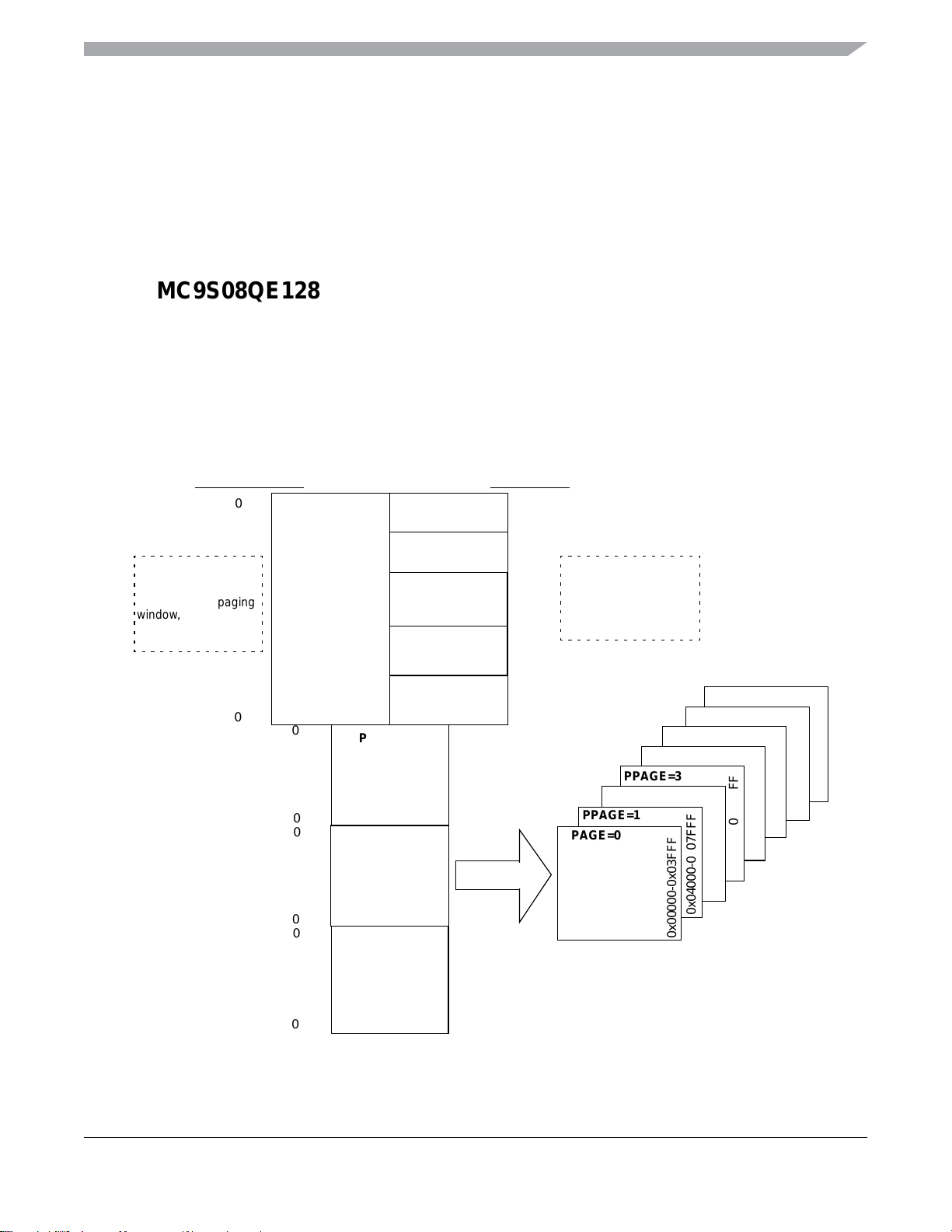
Chapter 4
+64K:
up to
128K
In the Figure 4-1,
BLUE arrows (for Program
and Constants), does NOT
depend on PPAGE; only
on: Logical 16 bit
address being OUT of
PAGE 2 range. Physical
A16 will always be "0".
RED arrows (program
and constants)
DOES DEPEND, indeed,
on both: PPAGE, and
Logical 16 bit address being INSIDE of
PAGE 2 range. If so,
Physical Address is:
PPAGE(2:0);A13:A0
A15:A14 are NEVER
used to form Physical
Address
This is why ISRs MUST
be located in pages 0,
1 or 3: they do NOT
use PPAGE, that is NOT
preserved over Interrupts. NEVER locate
ISRs in page 2.
Inside ISRs you may
use code located on
Banked Memory (Pages
2,4,5,6,7) employing
CALL/RTC to save
and restore PPAGE.
PPAGES values 0, 1 & 3
ARE NOT OF ANY USE!!
--0xFF: 128 Bytes Direct "Page" RAM,
(not in the sense of MMU 8 Pages...)
Completly modifyied, corrected, commented and augmented by Luis G. Uribe C. Mar/Jun 2012
Memory
4.1 MC9S08QE128 Series Memory Map
As shown in Figure 4-1, Figure 4-2, and Figure 4-3, on-chip memory in the MC9S08QE128 Series of
MCUs consists of RAM, flash program memory for nonvolatile data storage, and I/O and control/status
registers. The registers are divided into three groups:
• Direct-page registers (0x0000 through 0x007F)
• High-page registers (0x1800 through 0x187F)
• Nonvolatile registers (0xFFB0 through 0xFFBF)
Extended Address CPU Address
0x00000
When PPAGE 0 is
accessed through the
linear address pointer
or through the paging
window, the flash
memory is read.
0x03FFF
PPAGE=0
FLASH
16384 BYTES
0x04000
0x07FFF
0x08000
0x0BFFF
0x0C000
DIRECT PAGE
REGISTERS
128 BYTES
6016 BYTES
PAGE REGISTERS
128 BYTES
2048 BYTES
8064 BYTES
PPAGE=1
FLASH
16384 BYTES
Paging Window -
Extended addresses formed with
PPAGE and
A13:A0 of CPU address
PPAGE=3
RAM
HIGH
RAM
FLASH
0x4000
0x7FFF
0x8000
0xBFFF
0xC000
0x0000
0x007F
0x0080
0x17FF
0x1800
0x187F
0x1880
0x207F
0x2080
0x3FFF
When the CPU
accesses PPAGE 0
directly, RAM and
registers,whenpresent,
take priority over flash
memory.
PPAGE=5
PPAGE=4
PPAGE=3
PPAGE=2
PPAGE=1
PPAGE=0
FLASH
16384 BYTES
16384 BYTES
0x00000-0x03FFF
PPAGE=7
PPAGE=6
flash
0x10000-0x13FFF
0x0C000-0x0FFFF
0x08000-0x0BFFF
0x04000-0x07FFF
0x1C000-0x1FFFF
0x18000-0x1BFFF
0x14000-0x17FFF
FLASH
16384 BYTES
Freescale Semiconductor 51
0x0FFFF
Figure 4-1. MC9S08QE128 Memory Map
MC9S08QE128 MCU Series Reference Manual, Rev. 2
0xFFFF
Extended
Address
Page 51
Chapter 4
Original page 51...
Memory
4.1 MC9S08QE128 Series Memory Map
As shown in Figure 4-1, Figure 4-2, and Figure 4-3, on-chip memory in the MC9S08QE128 Series of
MCUs consists of RAM, flash program memory for nonvolatile data storage, and I/O and control/status
registers. The registers are divided into three groups:
• Direct-page registers (0x0000 through 0x007F)
• High-page registers (0x1800 through 0x187F)
• Nonvolatile registers (0xFFB0 through 0xFFBF)
Extended Address CPU Address
0x00000
When PPAGE 0 is
accessed through the
linear address pointer
or through the paging
window, the flash
memory is read.
0x03FFF
PPAGE=0
FLASH
16384 BYTES
0x04000
0x07FFF
0x08000
0x0BFFF
0x0C000
DIRECT PAGE
REGISTERS
128 BYTES
6016 BYTES
PAGE REGISTERS
128 BYTES
2048 BYTES
8064 BYTES
PPAGE=1
FLASH
16384 BYTES
Paging Window -
Extended addresses formed with
PPAGE and
A13:A0 of CPU address
PPAGE=3
RAM
HIGH
RAM
FLASH
0x4000
0x7FFF
0x8000
0xBFFF
0xC000
0x0000
0x007F
0x0080
0x17FF
0x1800
0x187F
0x1880
0x207F
0x2080
0x3FFF
When the CPU
accesses PPAGE 0
directly, RAM and
registers,whenpresent,
take priority over flash
memory.
PPAGE=5
PPAGE=4
PPAGE=3
PPAGE=2
PPAGE=1
PPAGE=0
FLASH
16384 BYTES
16384 BYTES
0x00000-0x03FFF
PPAGE=7
PPAGE=6
flash
0x10000-0x13FFF
0x0C000-0x0FFFF
0x08000-0x0BFFF
0x04000-0x07FFF
0x1C000-0x1FFFF
0x18000-0x1BFFF
0x14000-0x17FFF
Freescale Semiconductor 51
FLASH
16384 BYTES
0x0FFFF
0xFFFF
Figure 4-1. MC9S08QE128 Memory Map
MC9S08QE128 MCU Series Reference Manual, Rev. 2
Extended
Address
Page 52
Chapter 4 Memory
Extended Address CPU Address
When PPAGE 0 is
accessed through the
linear address pointer
or through the paging
window, the flash
memory is read.
0x00000
0x03FFF
PPAGE=0
FLASH
16384 BYTES
0x04000
0x07FFF
0x08000
0x0BFFF
0x0C000
DIRECT PAGE
REGISTERS
128 BYTES
6016 BYTES
PAGE REGISTERS
128 BYTES
RESERVED
2048 BYTES
8064 BYTES
PPAGE=1
FLASH
16384 BYTES
Paging Window -
Extended
addresses formed
with PPAGE and
A13:A0 of CPU
address
PPAGE=3
RAM
HIGH
FLASH
0x4000
0x7FFF
0x8000
0xBFFF
0xC000
0x0000
0x007F
0x0080
0x17FF
0x1800
0x187F
0x1880
0x207F
0x2080
0x3FFF
When the CPU
accesses PPAGE 0
directly, RAM and
registers,whenpresent,
take priority over flash
memory.
PPAGE=5
PPAGE=4
PPAGE=3
PPAGE=2
PPAGE=1
PPAGE=0
FLASH
16384 BYTES
FLASH
16384 BYTES
0x00000-0x03FFF
PPAGE=7
PPAGE=6
RESERVED
16384 BYTES
0x14000-0x17FFF
0x10000-0x13FFF
0x0C000-0x0FFFF
0x08000-0x0BFFF
0x04000-0x07FFF
0x1C000-0x1FFFF
0x18000-0x1BFFF
Address
Extended
0x0FFFF
FLASH
16384 BYTES
0xFFFF
Figure 4-2. MC9S08QE96 Memory Map
Extended
Address
MC9S08QE128 MCU Series Reference Manual, Rev. 2
52 Freescale Semiconductor
Page 53
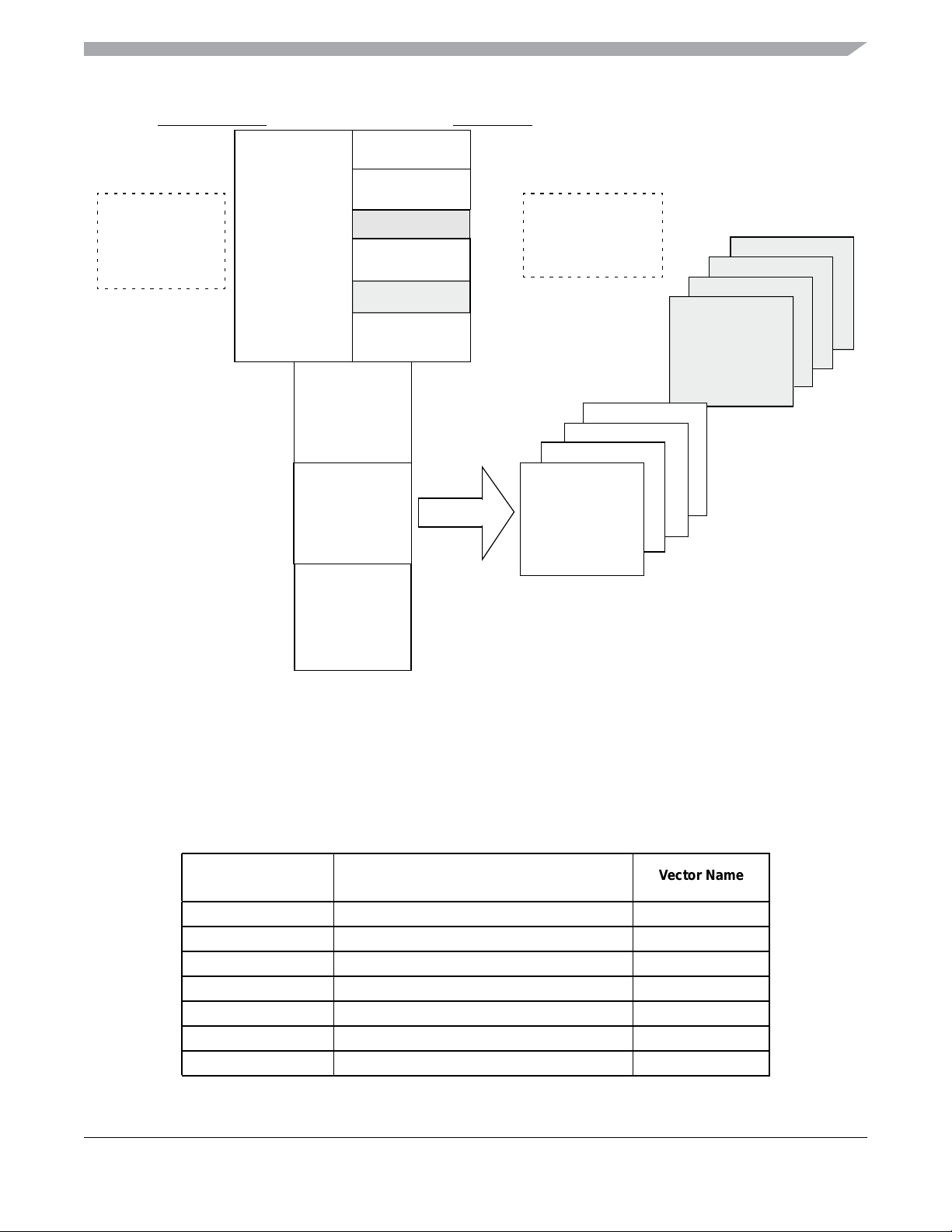
Extended Address CPU Address
0x00000
When PPAGE 0 is
accessed through the
linear address pointer
or through the paging
window, the flash
memory is read.
0x03FFF
PPAGE=0
FLASH
16384 BYTES
0x04000
0x07FFF
0x08000
0x0BFFF
0x0C000
DIRECT PAGE
REGISTERS
128 BYTES
4096 BYTES
RESERVED
1920 BYTES
PAGE REGISTERS
128 BYTES
RESERVED
2048 BYTES
8064 BYTES
PPAGE=1
FLASH
16384 BYTES
Paging Window -
Extended
addresses formed
with PPAGE and
A13:A0 of CPU
address
PPAGE=3
RAM
HIGH
FLASH
0x4000
0x7FFF
0x8000
0xBFFF
0xC000
0x0000
0x007F
0x0080
0x107F
0x1080
0x17FF
0x1800
0x187F
0x1880
0x207F
0x2080
0x3FFF
When the CPU
accesses PPAGE 0
directly, RAM and
registers,whenpresent,
take priority over flash
memory.
PPAGE=3
PPAGE=2
PPAGE=1
PPAGE=0
FLASH
16384 BYTES
0x00000-0x03FFF
PPAGE=7
PPAGE=6
PPAGE=5
PPAGE=4
0x08000-0x0BFFF
0x04000-0x07FFF
RESERVED
16384 BYTES
RESERVED
16384 BYTES
RESERVED
16384 BYTES
0x0C000-0x0FFFF
Chapter 4 Memory
0x1C000-0x1FFFF
0x18000-0x1BFFF
0x14000-0x17FFF
0x10000-0x13FFF
Extended
Address
FLASH
0x0FFFF
16384 BYTES
0xFFFF
Extended
Address
Figure 4-3. MC9S08QE64 Memory Map
4.2 Reset and Interrupt Vector Assignments
Table 4-1 shows address assignments for reset and interrupt vectors. The vector names shown in this table
are the labels used in the Freescale Semiconductor provided equate file for the MC9S08QE128 Series.
Table 4-1. Reset and Interrupt Vectors
Address
(High/Low)
0xFFC0:0xFFC1 TPM3 Overflow Vtpm3ovf
0xFFC2:0xFFC3 TPM3 Channel 5 Vtpm3ch5
0xFFC4:0xFFC5 TPM3 Channel 4 Vtpm3ch4
0xFFC6:0xFFC7 TPM3 Channel 3 Vtpm3ch3
0xFFC8:0xFFC9 TPM3 Channel 2 Vtpm3ch2
0xFFCA:0xFFCB TPM3 Channel 1 Vtpm3ch1
0xFFCC:0xFFCD TPM3 Channel 0 Vtpm3ch0
Vector Vector Name
MC9S08QE128 MCU Series Reference Manual, Rev. 2
Freescale Semiconductor 53
Page 54

Chapter 4 Memory
Table 4-1. Reset and Interrupt Vectors (continued)
Address
(High/Low)
Vector Vector Name
0xFFCE:0xFFCF RTC Vrtc
0xFFD0:0xFFD1 SCI2 Transmit Vsci2tx
0xFFD2:0xFFD3 SCI2 Receive Vsci2rx
0xFFD4:0xFFD5 SCI2 Error Vsci2err
0xFFD6:0xFFD7 ACMPx
1
Vacmpx
0xFFD8:0xFFD9 ADC Conversion Vadc
0xFFDA:0xFFDB KBIx Interrupt
0xFFDC:0xFFDD IICx
3
2
Vkeyboard
Viicx
0xFFDE:0xFFDF SCI1 Transmit Vsci1tx
0xFFE0:0xFFE1 SCI1 Receive Vsci1rx
0xFFE2:0xFFE3 SCI1 Error Vsci1err
0xFFE4:0xFFE5 SPI1 Vspi1
0xFFE6:0xFFE7 SPI2 Vspi2
0xFFE8:0xFFE9 TPM2 Overflow Vtpm2ovf
0xFFEA:0xFFEB TPM2 Channel 2 Vtpm2ch2
0xFFEC:0xFFED TPM2 Channel 1 Vtpm2ch1
0xFFEE:0xFFEF TPM2 Channel 0 Vtpm2ch0
0xFFF0:0xFFF1 TPM1 Overflow Vtpm1ovf
0xFFF2:0xFFF3 TPM1 Channel 2 Vtpm1ch2
0xFFF4:0xFFF5 TPM1 Channel 1 Vtpm1ch1
0xFFF6:0xFFF7 TPM1 Channel 0 Vtpm1ch0
0xFFF8:0xFFF9 Low Voltage Detect or Low Voltage Warning Vlvd
0xFFFA:0xFFFB IRQ Virq
0xFFFC:0xFFFD SWI Vswi
0xFFFE:0xFFFF Reset Vreset
1
ACMP1 and ACMP2 share this vector,if both modules are enabled user should poll each flag
to determine pending interrupt.
2
KBI1 and KBI2 share this vector, if both modules are enabled user should poll each flag to
determine pending interrupt.
3
IIC1 and IIC2 share this vector, if both modules are enabled user should poll each flag to
determine pending interrupt.
MC9S08QE128 MCU Series Reference Manual, Rev. 2
54 Freescale Semiconductor
Page 55

Chapter 4 Memory
4.3 Register Addresses and Bit Assignments
The registers in the MC9S08QE128 Series are divided into these groups:
• Direct-page registers are located in the first 128 locations in the memory map; these are accessible
with efficient direct addressing mode instructions.
• High-page registers are used much less often, so they are located above 0x1800 in the memory
map. This leaves more room in the direct page for more frequently used registers and RAM.
• The nonvolatile register area consists of a block of 16 locations in flash memory at
0xFFB0–0xFFBF. Nonvolatile register locations include:
— NVPROT and NVOPT are loaded into working registers at reset
— An 8-byte backdoor comparison key that optionally allows a user to gain controlled access to
secure memory
Because the nonvolatile register locations are flash memory, they must be erased and programmed
like other flash memory locations.
Direct-page registers can be accessed with efficient direct addressing mode instructions. Bit manipulation
instructions can be used to access any bit in any direct-page register.
user-accessible direct-page registers and control bits.
Table 4-2 is a summary of all
The direct page registers in Table 4-2 can use the more efficient direct addressing mode, which requires
only the lower byte of the address. Because of this, the lower byte of the address in column one is shown
in bold text. In Table 4-3 and Table 4-4, the whole address in column one is shown in bold. In Table 4-2,
Table 4-3, and Table 4-4, the register names in column two are shown in bold to set them apart from the
bit names to the right. Cells that are not associated with named bits are shaded. A shaded cell with a 0
indicates this unused bit always reads as a 0. Shaded cells with dashes indicate unused or reserved bit
locations that could read as 1s or 0s. When writing to these bits, write a 0 unless otherwise specified.
MC9S08QE128 MCU Series Reference Manual, Rev. 2
Freescale Semiconductor 55
Page 56
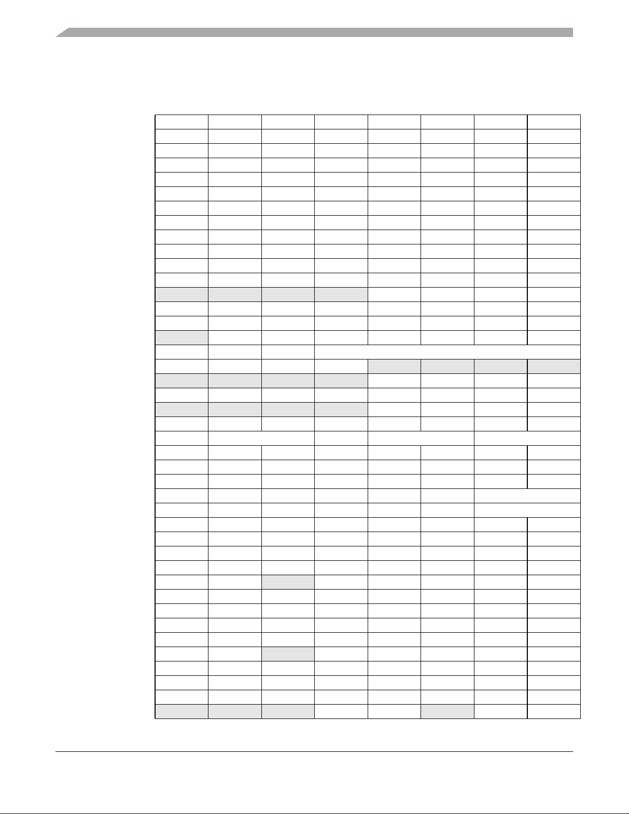
Chapter 4 Memory
Table 4-2. Direct-Page Register Summary (Sheet 1 of 4)
Address
0x0000 PTAD PTAD7 PTAD6 PTAD5 PTAD4 PTAD3 PTAD2 PTAD1 PTAD0
0x0001 PTADD PTADD7 PTADD6 PTADD5 PTADD4 PTADD3 PTADD2 PTADD1 PTADD0
0x0002 PTBD PTBD7 PTBD6 PTBD5 PTBD4 PTBD3 PTBD2 PTBD1 PTBD0
0x0003 PTBDD PTBDD7 PTBDD6 PTBDD5 PTBDD4 PTBDD3 PTBDD2 PTBDD1 PTBDD0
0x0004 PTCD PTCD7 PTCD6 PTCD5 PTCD4 PTCD3 PTCD2 PTCD1 PTCD0
0x0005 PTCDD PTCDD7 PTCDD6 PTCDD5 PTCDD4 PTCDD3 PTCDD2 PTCDD1 PTCDD0
0x0006 PTDD PTDD7 PTDD6 PTDD5 PTDD4 PTDD3 PTDD2 PTDD1 PTDD0
0x0007 PTDDD PTDDD7 PTDDD6 PTDDD5 PTDDD4 PTDDD3 PTDDD2 PTDDD1 PTDDD0
0x0008 PTED PTED7 PTED6 PTED5 PTED4 PTED3 PTED2 PTED1 PTED0
0x0009 PTEDD PTEDD7 PTEDD6 PTEDD5 PTEDD4 PTEDD3 PTEDD2 PTEDD1 PTEDD0
0x000A PTFD PTFD7 PTFD6 PTFD5 PTFD4 PTFD3 PTFD2 PTFD1 PTFD0
0x000B PTFDD PTFDD7 PTFDD6 PTFDD5 PTFDD4 PTFDD3 PTFDD2 PTFDD1 PTFDD0
0x000C KBI1SC
0x000D KBI1PE KBIPE7 KBIPE6 KBIPE5 KBIPE4 KBIPE3 KBIPE2 KBIPE1 KBIPE0
0x000E KBI1ES KBEDG7 KBEDG6 KBEDG5 KBEDG4 KBEDG3 KBEDG2 KBEDG1 KBEDG0
0x000F IRQSC
0x0010 ADCSC1 COCO AIEN ADCO ADCH
0x0011 ADCSC2 ADACT ADTRG ACFE ACFGT
0x0012 ADCRH
0x0013 ADCRL ADR7 ADR6 ADR5 ADR4 ADR3 ADR2 ADR1 ADR0
0x0014 ADCCVH
0x0015 ADCCVL ADCV7 ADCV6 ADCV5 ADCV4 ADCV3 ADCV2 ADCV1 ADCV0
0x0016 ADCCFG ADLPC ADIV ADLSMP MODE ADICLK
0x0017 APCTL1 ADPC7 ADPC6 ADPC5 ADPC4 ADPC3 ADPC2 ADPC1 ADPC0
0x0018 APCTL2 ADPC15 ADPC14 ADPC13 ADPC12 ADPC11 ADPC10 ADPC9 ADPC8
0x0019 APCTL3 ADPC23 ADPC22 ADPC21 ADPC20 ADPC19 ADPC18 ADPC17 ADPC16
0x001A ACMP1SC ACME ACBGS ACF ACIE ACO ACOPE ACMOD
0x001B ACMP2SC ACME ACBGS ACF ACIE ACO ACOPE ACMOD
0x001C PTGD PTGD7 PTGD6 PTGD5 PTGD4 PTGD3 PTGD2 PTGD1 PTGD0
0x001D PTGDD PTGDD7 PTGDD6 PTGDD5 PTGDD4 PTGDD3 PTGDD2 PTGDD1 PTGDD0
0x001E PTHD PTHD7 PTHD6 PTHD5 PTHD4 PTHD3 PTHD2 PTHD1 PTHD0
0x001F PTHDD PTHDD7 PTHDD6 PTHDD5 PTHDD4 PTHDD3 PTHDD2 PTHDD1 PTHDD0
0x0020 SCI1BDH LBKDIE RXEDGIE
0x0021 SCI1BDL SBR7 SBR6 SBR5 SBR4 SBR3 SBR2 SBR1 SBR0
0x0022 SCI1C1 LOOPS SCISWAI RSRC M WAKE ILT PE PT
0x0023 SCI1C2 TIE TCIE RIE ILIE TE RE RWU SBK
0x0024 SCI1S1 TDRE TC RDRF IDLE OR NF FE PF
0x0025 SCI1S2 LBKDIF RXEDGIF
0x0026 SCI1C3 R8 T8 TXDIR TXINV ORIE NEIE FEIE PEIE
0x0027 SCI1D Bit 7 654321Bit 0
0x0028 SPI1C1 SPIE SPE SPTIE MSTR CPOL CPHA SSOE LSBFE
0x0029 SPI1C2
Register
Name
Bit 7 654321Bit 0
0 0 0 0 KBF KBACK KBIE KBIMOD
0 IRQPDD IRQEDG IRQPE IRQF IRQACK IRQIE IRQMOD
— — Reserved Reserved
0 0 0 0 ADR11 ADR10 ADR9 ADR8
0 0 0 0 ADCV11 ADCV10 ADCV9 ADCV8
0 SBR12 SBR11 SBR10 SBR9 SBR8
0 RXINV RWUID BRK13 LBKDE RAF
0 0 0 MODFEN BIDIROE 0 SPISWAI SPC0
MC9S08QE128 MCU Series Reference Manual, Rev. 2
56 Freescale Semiconductor
Page 57
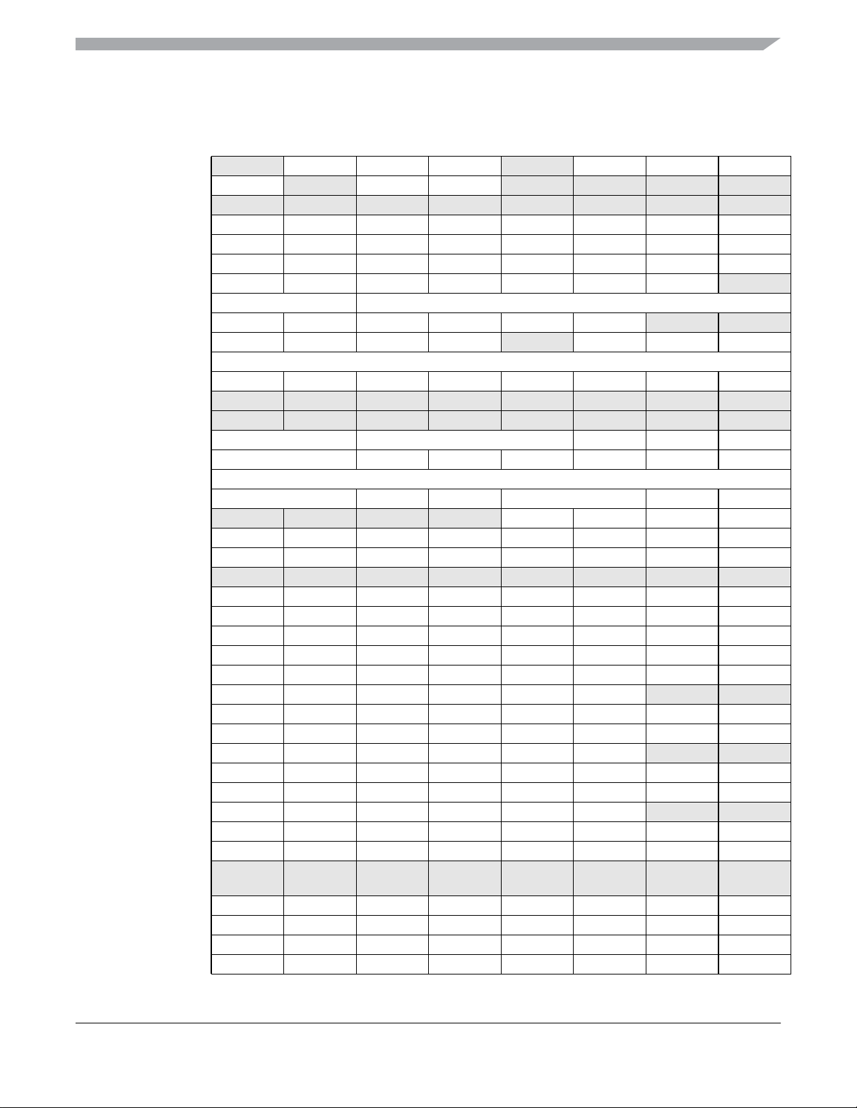
Table 4-2. Direct-Page Register Summary (Sheet 2 of 4)
Chapter 4 Memory
Address
0x002A SPI1BR
0x002B SPI1S SPRF
0x002C Reserved
0x002D SPI1D Bit 7 654321Bit 0
0x002E PTJD PTJD7 PTJD6 PTJD5 PTJD4 PTJD3 PTJD2 PTJD1 PTJD0
0x002F PTJDD PTJDD7 PTJDD6 PTJDD5 PTJDD4 PTJDD3 PTJDD2 PTJDD1 PTJDD0
0x0030 IIC1A AD7 AD6 AD5 AD4 AD3 AD2 AD1
0x0031 IIC1F MULT ICR
0x0032 IIC1C1 IICEN IICIE MST TX TXAK RSTA
0x0033 IIC1S TCF IAAS BUSY ARBL
0x0034 IIC1D DA TA
0x0035 IIC1C2 GCAEN ADEXT 0 0 0 AD10 AD9 AD8
0x0036 Reserved
0x0037 Reserved
0x0038 ICSC1 CLKS RDIV IREFS IRCLKEN IREFSTEN
0x0039 ICSC2 BDIV RANGE HGO LP EREFS ERCLKEN EREFSTEN
0x003A ICSTRM TRIM
0x003B ICSSC DRS/DRST DMX32 IREFST CLKST OSCINIT FTRIM
0x003C KBI2SC
0x003D KBI2PE KBIPE7 KBIPE6 KBIPE5 KBIPE4 KBIPE3 KBIPE2 KBIPE1 KBIPE0
0x003E KBI2ES KBEDG7 KBEDG6 KBEDG5 KBEDG4 KBEDG3 KBEDG2 KBEDG1 KBEDG0
0x003F Reserved
0x0040 TPM1SC TOF TOIE CPWMS CLKSB CLKSA PS2 PS1 PS0
0x0041 TPM1CNTH Bit 15 14 13 12 11 10 9 Bit 8
0x0042 TPM1CNTL Bit 7 654321Bit 0
0x0043 TPM1MODH Bit 15 14 13 12 11 10 9 Bit 8
0x0044 TPM1MODL Bit 7 654321Bit 0
0x0045 TPM1C0SC CH0F CH0IE MS0B MS0A ELS0B ELS0A
0x0046 TPM1C0VH Bit 15 14 13 12 11 10 9 Bit 8
0x0047 TPM1C0VL Bit 7 654321Bit 0
0x0048 TPM1C1SC CH1F CH1IE MS1B MS1A ELS1B ELS1A
0x0049 TPM1C1VH Bit 15 14 13 12 11 10 9 Bit 8
0x004A TPM1C1VL Bit 7 654321Bit 0
0x004B TPM1C2SC CH2F CH2IE MS2B MS2A ELS2B ELS2A
0x004C TPM1C2VH Bit 15 14 13 12 11 10 9 Bit 8
0x004D TPM1C2VL Bit 7 654321Bit 0
0x004E-
0x004F
0x0050 TPM2SC TOF TOIE CPWMS CLKSB CLKSA PS2 PS1 PS0
0x0051 TPM2CNTH Bit 15 14 13 12 11 10 9 Bit 8
0x0052 TPM2CNTL Bit 7 654321Bit 0
0x0053 TPM2MODH Bit 15 14 13 12 11 10 9 Bit 8
Register
Name
Reserved
Bit 7 654321Bit 0
0 SPPR2 SPPR1 SPPR0 0 SPR2 SPR1 SPR0
0 SPTEF MODF 0 0 0 0
0 0 0 0 0 0 0 0
0
0 0
0 SRW IICIF RXAK
— — — — — — — —
— — — — — — — —
0 0 0 0 KBF KBACK KBIE KBIMOD
— — — — — — — —
0 0
0 0
0 0
—
—
—
—
—
—
—
—
—
—
—
—
—
—
—
—
MC9S08QE128 MCU Series Reference Manual, Rev. 2
Freescale Semiconductor 57
Page 58
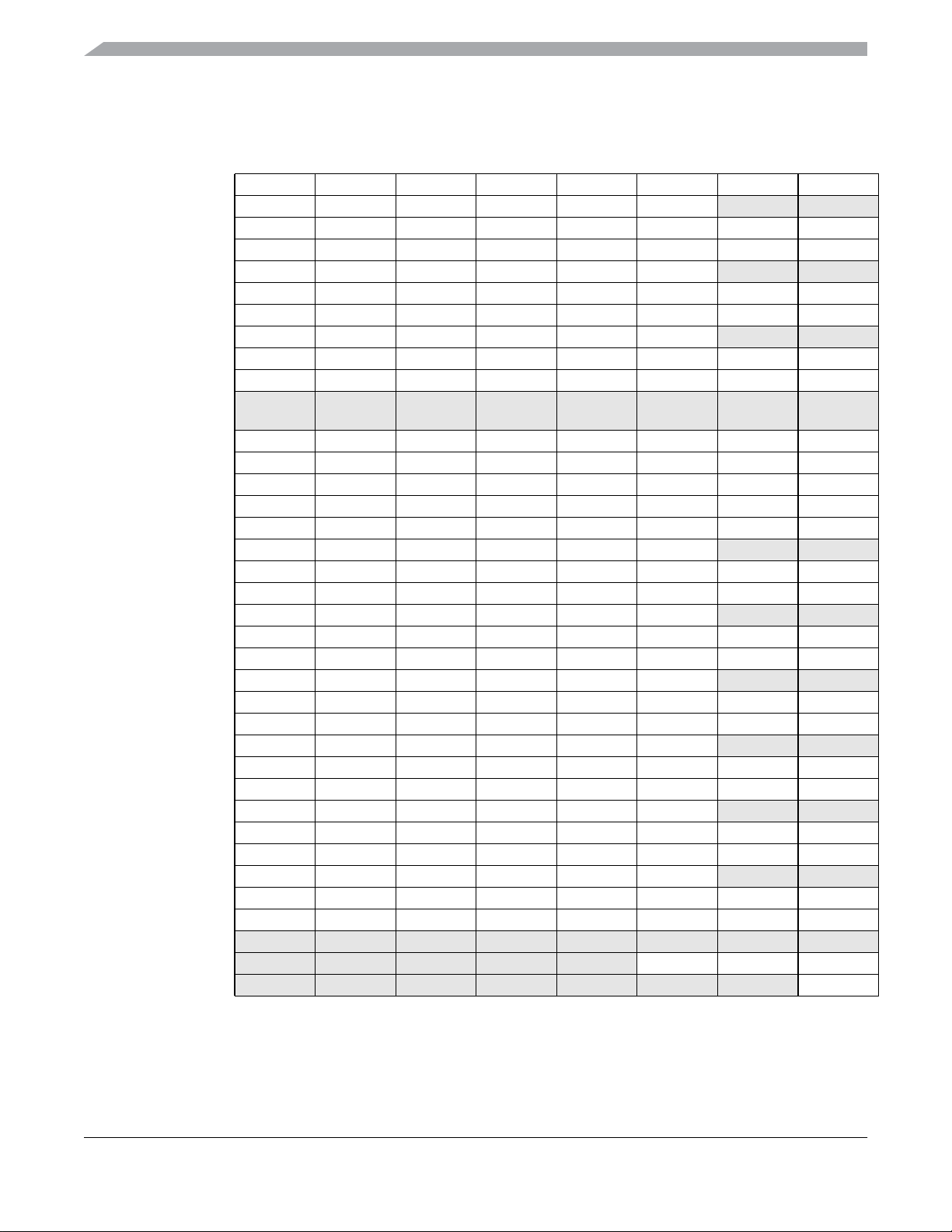
Chapter 4 Memory
Table 4-2. Direct-Page Register Summary (Sheet 3 of 4)
Address
0x0054 TPM2MODL Bit 7 654321Bit 0
0x0055 TPM2C0SC CH0F CH0IE MS0B MS0A ELS0B ELS0A
0x0056 TPM2C0VH Bit 15 14 13 12 11 10 9 Bit 8
0x0057 TPM2C0VL Bit 7 654321Bit 0
0x0058 TPM2C1SC CH1F CH1IE MS1B MS1A ELS1B ELS1A
0x0059 TPM2C1VH Bit 15 14 13 12 11 10 9 Bit 8
0x005A TPM2C1VL Bit 7 654321Bit 0
0x005B TPM2C2SC CH2F CH2IE MS2B MS2A ELS2B ELS2A
0x005C TPM2C2VH Bit 15 14 13 12 11 10 9 Bit 8
0x005D TPM2C2VL Bit 7 654321Bit 0
0x005E-
0x005F
0x0060 TPM3SC TOF TOIE CPWMS CLKSB CLKSA PS2 PS1 PS0
0x0061 TPM3CNTH Bit 15 14 13 12 11 10 9 Bit 8
0x0062 TPM3CNTL Bit 7 654321Bit 0
0x0063 TPM3MODH Bit 15 14 13 12 11 10 9 Bit 8
0x0064 TPM3MODL Bit 7 654321Bit 0
0x0065 TPM3C0SC CH0F CH0IE MS0B MS0A ELS0B ELS0A
0x0066 TPM3C0VH Bit 15 14 13 12 11 10 9 Bit 8
0x0067 TPM3C0VL Bit 7 654321Bit 0
0x0068 TPM3C1SC CH1F CH1IE MS1B MS1A ELS1B ELS1A
0x0069 TPM3C1VH Bit 15 14 13 12 11 10 9 Bit 8
0x006A TPM3C1VL Bit 7 654321Bit 0
0x006B TPM3C2SC CH2F CH2IE MS2B MS2A ELS2B ELS2A
0x006C TPM3C2VH Bit 15 14 13 12 11 10 9 Bit 8
0x006D TPM3C2VL Bit 7 654321Bit 0
0x006E TPM3C3SC CH3F CH3IE MS3B MS3A ELS3B ELS3A
0x006F TPM3C3VH Bit 15 14 13 12 11 10 9 Bit 8
0x0070 TPM3C3VL Bit 7 654321Bit 0
0x0071 TPM3C4SC CH4F CH4IE MS4B MS4A ELS4B ELS4A
0x0072 TPM3C4VH Bit 15 14 13 12 11 10 9 Bit 8
0x0073 TPM3C4VL Bit 7 654321Bit 0
0x0074 TPM3C5SC CH5F CH5IE MS5B MS5A ELS5B ELS5A
0x0075 TPM3C5VH Bit 15 14 13 12 11 10 9 Bit 8
0x0076 TPM3C5VL Bit 7 654321Bit 0
0x0077 Reserved
0x0078 PPAGE
0x0079 LAP2
Register
Name
Reserved
Bit 7 654321Bit 0
0 0
0 0
0 0
—
—
— — — — — — — —
0 0 0 0 0 XA16 XA15 XA14
0 0 0 0 0 0 0 LA16
—
—
—
—
—
—
—
—
—
—
—
—
0 0
0 0
0 0
0 0
0 0
0 0
—
—
MC9S08QE128 MCU Series Reference Manual, Rev. 2
58 Freescale Semiconductor
Page 59
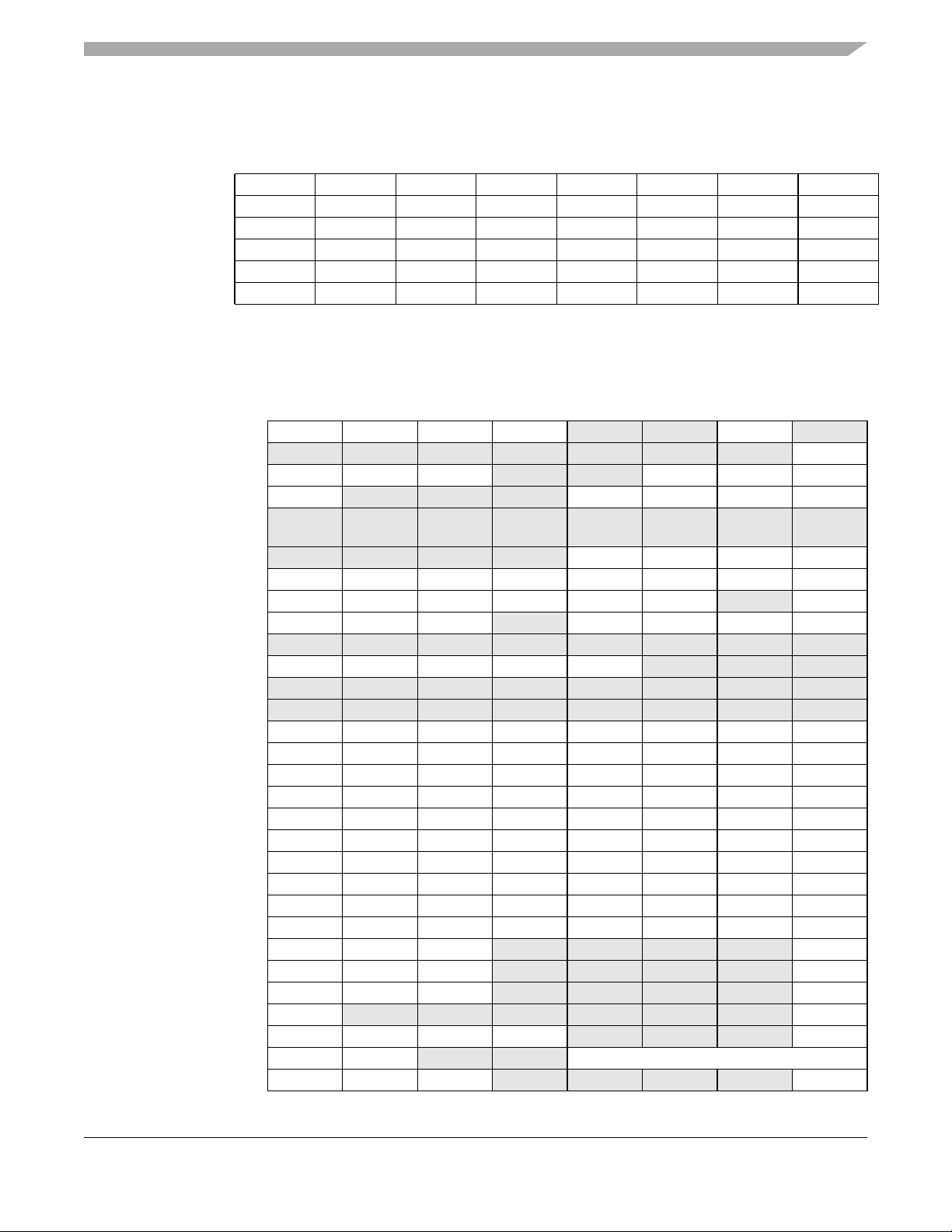
Table 4-2. Direct-Page Register Summary (Sheet 4 of 4)
Chapter 4 Memory
Address
0x007A LAP1 LA15 LA14 LA13 LA12 LA11 LA10 LA9 LA8
0x007B LAP0 LA7 LA6 LA5 LA4 LA3 LA2 LA1 LA0
0x007C LWP D7 D6 D5 D4 D3 D2 D1 D0
0x007D LBP D7 D6 D5 D4 D3 D2 D1 D0
0x007E LB D7 D6 D5 D4 D3 D2 D1 D0
0x007F LAPAB D7 D6 D5 D4 D3 D2 D1 D0
Register
Name
Bit 7 654321Bit 0
High-page registers, shown in Table 4-3, are accessed much less often than other I/O and control registers
so they have been located outside the direct addressable memory space, starting at 0x1800.
Table 4-3. High-Page Register Summary (Sheet 1 of 4)
Address Register Name Bit 7 654321Bit 0
0x1800 SRS POR PIN COP ILOP
0x1801 SBDFR
0x1802 SOPT1 COPE COPT STOPE
0x1803 SOPT2 COPCLKS
0x1804 –
0x1805
0x1806 SDIDH
0x1807 SDIDL ID7 ID6 ID5 ID4 ID3 ID2 ID1 ID0
0x1808 SPMSC1 LVDF LVDACK LVDIE LVDRE LVDSE LVDE
0x1809 SPMSC2 LPR LPRS LPWUI
0x180A Reserved
0x180B SPMSC3 LVWF LVWACK LVDV LVWV LVWIE
0x180C Reserved
0x180D Reserved
0x180E SCGC1 TPM3 TPM2 TPM1 ADC IIC2 IIC1 SCI2 SCI1
0x180F SCGC2 DBG FLS IRQ KBI ACMP RTC SPI2 SPI1
0x1810 DBGCAH Bit 15 14 13 12 11 10 9 Bit 8
0x1811 DBGCAL Bit 7 654321Bit 0
0x1812 DBGCBH Bit 15 14 13 12 11 10 9 Bit 8
0x1813 DBGCBL Bit 7 654321Bit 0
0x1814 DBGCCH Bit 15 14 13 12 11 10 9 Bit 8
0x1815 DBGCCL Bit 7 654321Bit 0
0x1816 DBGFH Bit 15 14 13 12 11 10 9 Bit 8
0x1817 DBGFL Bit 7 654321Bit 0
0x1818 DBGCAX RWAEN RWA PAGSEL
0x1819 DBGCBX RWBEN RWB PAGSEL
0x181A DBGCCX RWCEN RWC PAGSEL
0x181B DBGFX PPACC
0x181C DBGC DBGEN ARM TAG BRKEN
0x181D DBGT TRGSEL BEGIN
0x181E DBGS AF BF CF
Reserved
0 0 0 0 0 0 0 BDFR
— 0 RSTPOE BKGDPE RSTPE
0 0 0 SPI1PS ACIC2 IIC1PS ACIC1
—
—
— — — — ID11 ID10 ID9 ID8
— — — — — — — —
— — — — — — — —
— — — — — — — —
—
—
0 0 0 0 0 0 Bit 16
—
—
0 0 TRG
—
—
0 PPDF PPDACK PPDE PPDC
0 0 0 0 Bit 16
0 0 0 0 Bit 16
0 0 0 0 Bit 16
0 0 0 0 ARMF
0 0LVD0
—
—
0 0 0 LOOP1
—
—
— — —
—
—
0 BGBE
—
—
MC9S08QE128 MCU Series Reference Manual, Rev. 2
Freescale Semiconductor 59
Page 60
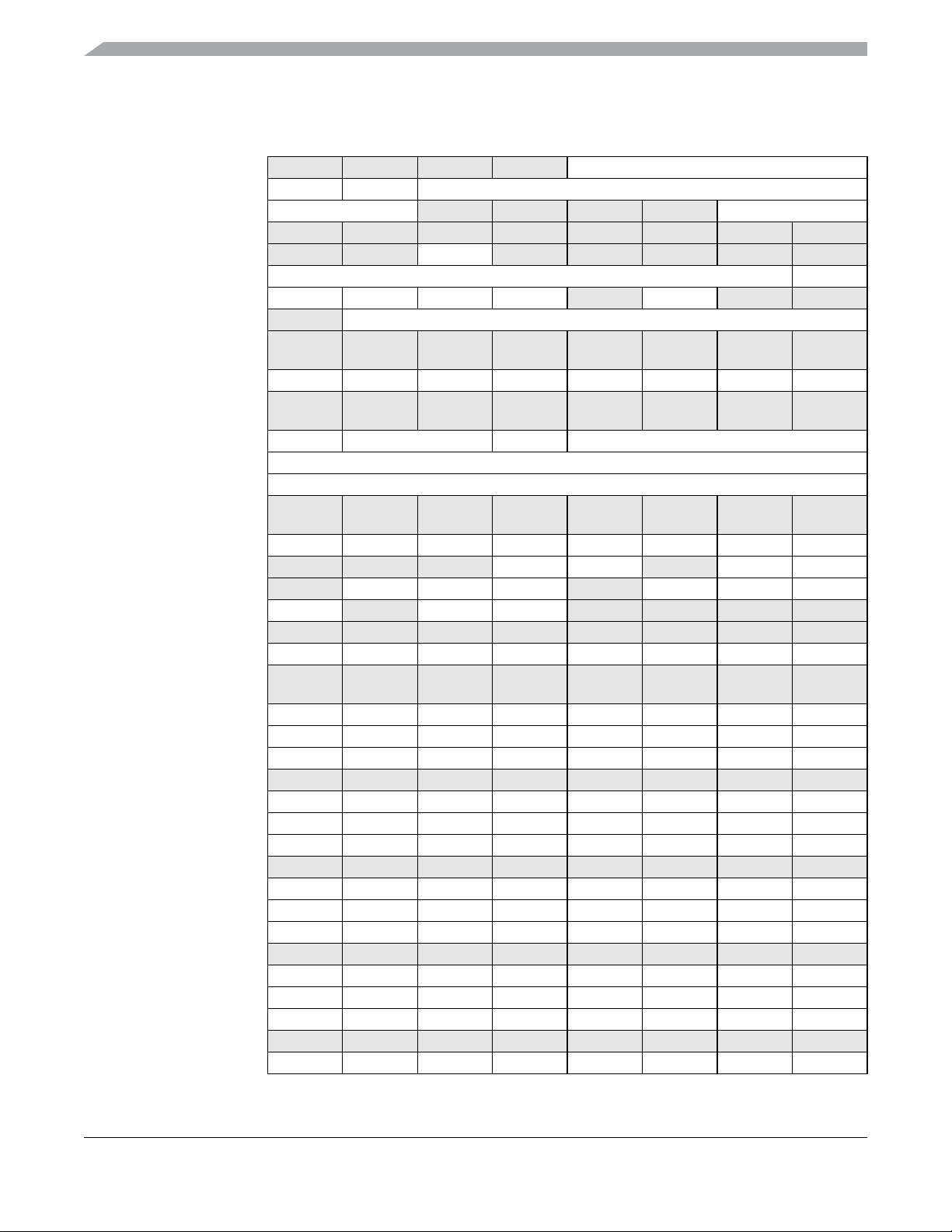
Chapter 4 Memory
Table 4-3. High-Page Register Summary (Sheet 2 of 4)
Address Register Name Bit 7 654321Bit 0
0x181F DBGCNT
0x1820 FCDIV FDIVLD PRDIV8 FDIV
0x1821 FOPT KEYEN
0x1822 Reserved
0x1823 FCNFG
0x1824 FPROT FPS FPOPEN
0x1825 FSTAT FCBEF FCCF FPVIOL FACCERR
0x1826 FCMD
0x1827-
0x1829
0x182A Reserved
0x182B-
0x182F
0x1830 RTCSC RTIF RTCLKS RTIE RTCPS
0x1831 RTCCNT RTCCNT
0x1832 RTCMOD RTCMOD
0x1833-
0x1837
0x1838 SPI2C1 SPIE SPE SPTIE MSTR CPOL CPHA SSOE LSBFE
0x1839 SPI2C2
0x183A SPI2BR
0x183B SPI2S SPRF
0x183C Reserved
0x183D SPI2D Bit 7 654321Bit 0
0x183E-
0x183F
0x1840 PTAPE PTAPE7 PTAPE6 PTAPE5 PTAPE4 PTAPE3 PTAPE2 PTAPE1 PTAPE0
0x1841 PTASE PTASE7 PTASE6 PTASE5 PTASE4 PTASE3 PTASE2 PTASE1 PTASE0
0x1842 PTADS PTADS7 PTADS6 PTADS5 PTADS4 PTADS3 PTADS2 PTADS1 PTADS0
0x1843 Reserved
0x1844 PTBPE PTBPE7 PTBPE6 PTBPE5 PTBPE4 PTBPE3 PTBPE2 PTBPE1 PTBPE0
0x1845 PTBSE PTBSE7 PTBSE6 PTBSE5 PTBSE4 PTBSE3 PTBSE2 PTBSE1 PTBSE0
0x1846 PTBDS PTBDS7 PTBDS6 PTBDS5 PTBDS4 PTBDS3 PTBDS2 PTBDS1 PTBDS0
0x1847 Reserved
0x1848 PTCPE PTCPE7 PTCPE6 PTCPE5 PTCPE4 PTCPE3 PTCPE2 PTCPE1 PTCPE0
0x1849 PTCSE PTCSE7 PTCSE6 PTCSE5 PTCSE4 PTCSE3 PTCSE2 PTCSE1 PTCSE0
0x184A PTCDS PTCDS7 PTCDS6 PTCDS5 PTCDS4 PTCDS3 PTCDS2 PTCDS1 PTCDS0
0x184B Reserved
0x184C PTDPE PTDPE7 PTDPE6 PTDPE5 PTDPE4 PTDPE3 PTDPE2 PTDPE1 PTDPE0
0x184D PTDSE PTDSE7 PTDSE6 PTDSE5 PTDSE4 PTDSE3 PTDSE2 PTDSE1 PTDSE0
0x184E PTDDS PTDDS7 PTDDS6 PTDDS5 PTDDS4 PTDDS3 PTDDS2 PTDDS1 PTDDS0
0x184F Reserved
0x1850 PTEPE PTEPE7 PTEPE6 PTEPE5 PTEPE4 PTEPE3 PTEPE2 PTEPE1 PTEPE0
Reserved
Reserved
Reserved
Reserved
0 0 0 0 CNT
0 0 0 0 SEC
— — — — — — — —
0 0 KEYACC 0 0 0 0 0
0 FBLANK 0 0
0 FCMD
—
—
— — — — — — — —
—
—
0 0 0 MODFEN BIDIROE 0 SPISWAI SPC0
0 SPPR2 SPPR1 SPPR0 0 SPR2 SPR1 SPR0
0 0 0 0 0 0 0 0
—
—
— — — — — — — —
— — — — — — — —
— — — — — — — —
— — — — — — — —
—
—
—
—
0 SPTEF MODF 0 0 0 0
—
—
—
—
—
—
—
—
—
—
—
—
—
—
—
—
—
—
—
—
—
—
—
—
—
—
—
—
—
—
—
—
—
—
—
—
—
—
MC9S08QE128 MCU Series Reference Manual, Rev. 2
60 Freescale Semiconductor
Page 61
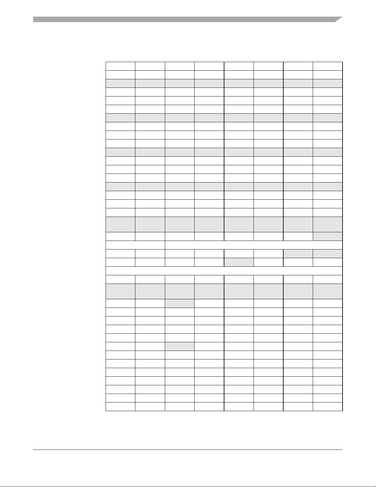
Chapter 4 Memory
Table 4-3. High-Page Register Summary (Sheet 3 of 4)
Address Register Name Bit 7 654321Bit 0
0x1851 PTESE PTESE7 PTESE6 PTESE5 PTESE4 PTESE3 PTESE2 PTESE1 PTESE0
0x1852 PTEDS PTEDS7 PTEDS6 PTEDS5 PTEDS4 PTEDS3 PTEDS2 PTEDS1 PTEDS0
0x1853 Reserved
0x1854 PTFPE PTFPE7 PTFPE6 PTFPE5 PTFPE4 PTFPE3 PTFPE2 PTFPE1 PTFPE0
0x1855 PTFSE PTFSE7 PTFSE6 PTFSE5 PTFSE4 PTFSE3 PTFSE2 PTFSE1 PTFSE0
0x1856 PTFDS PTFDS7 PTFDS6 PTFDS5 PTFDS4 PTFDS3 PTFDS2 PTFDS1 PTFDS0
0x1857 Reserved
0x1858 PTGPE PTGPE7 PTGPE6 PTGPE5 PTGPE4 PTGPE3 PTGPE2 PTGPE1 PTGPE0
0x1859 PTGSE PTGSE7 PTGSE6 PTGSE5 PTGSE4 PTGSE3 PTGSE2 PTGSE1 PTGSE0
0x185A PTGDS PTGDS7 PTGDS6 PTGDS5 PTGDS4 PTGDS3 PTGDS2 PTGDS1 PTGDS0
0x185B Reserved
0x185C PTHPE PTHPE7 PTHPE6 PTHPE5 PTHPE4 PTHPE3 PTHPE2 PTHPE1 PTHPE0
0x185D PTHSE PTHSE7 PTHSE6 PTHSE5 PTHSE4 PTHSE3 PTHSE2 PTHSE1 PTHSE0
0x185E PTHDS PTHDS7 PTHDS6 PTHDS5 PTHDS4 PTHDS3 PTHDS2 PTHDS1 PTHDS0
0x185F Reserved
0x1860 PTJPE PTJPE7 PTJPE6 PTJPE5 PTJPE4 PTJPE3 PTJPE2 PTJPE1 PTJPE0
0x1861 PTJSE PTJSE7 PTJSE6 PTJSE5 PTJSE4 PTJSE3 PTJSE2 PTJSE1 PTJSE0
0x1862 PTJDS PTJDS7 PTJDS6 PTJDS5 PTJDS4 PTJDS3 PTJDS2 PTJDS1 PTJDS0
0x1863–
0x1867
0x1868 IIC2A AD7 AD6 AD5 AD4 AD3 AD2 AD1
0x1869 IIC2F MULT ICR
0x186A IIC2C1 IICEN IICIE MST TX TXAK RSTA
0x186B IIC2S TCF IAAS BUSY ARBL
0x186C IIC2D DA TA
0x186D IIC2C2 GCAEN ADEXT 0 0 0 AD10 AD9 AD8
0x186E–
0x186F
0x1870 SCI2BDH LBKDIE RXEDGIE
0x1871 SCI2BDL SBR7 SBR6 SBR5 SBR4 SBR3 SBR2 SBR1 SBR0
0x1872 SCI2C1 LOOPS SCISWAI RSRC M WAKE ILT PE PT
0x1873 SCI2C2 TIE TCIE RIE ILIE TE RE RWU SBK
0x1874 SCI2S1 TDRE TC RDRF IDLE OR NF FE PF
0x1875 SCI2S2 LBKDIF RXEDGIF
0x1876 SCI2C3 R8 T8 TXDIR TXINV ORIE NEIE FEIE PEIE
0x1877 SCI2D Bit 7 654321Bit 0
0x1878 PTCSET PTCSET7 PTCSET6 PTCSET5 PTCSET4 PTCSET3 PTCSET2 PTCSET1 PTCSET0
0x1879 PTESET PTESET7 PTESET6 PTESET5 PTESET4 PTESET3 PTESET2 PTESET1 PTESET0
0x187A PTCCLR PTCCLR7 PTCCLR6 PTCCLR5 PTCCLR4 PTCCLR3 PTCCLR2 PTCCLR1 PTCCLR0
0x187B PTECLR PTECLR7 PTECLR6 PTECLR5 PTECLR4 PTECLR3 PTECLR2 PTECLR1 PTECLR0
0x187C PTCTOG PTCTOG7 PTCTOG6 PTCTOG5 PTCTOG4 PTCTOG3 PTCTOG2 PTCTOG1 PTCTOG0
Reserved
Reserved
— — — — — — — —
— — — — — — — —
— — — — — — — —
— — — — — — — —
—
—
—
—
—
—
—
—
—
—
—
—
0 SBR12 SBR11 SBR10 SBR9 SBR8
0 RXINV RWUID BRK13 LBKDE RAF
—
—
—
—
—
—
0 SRW IICIF RXAK
—
—
—
—
—
—
—
—
0 0
—
—
—
—
—
—
0
MC9S08QE128 MCU Series Reference Manual, Rev. 2
Freescale Semiconductor 61
Page 62
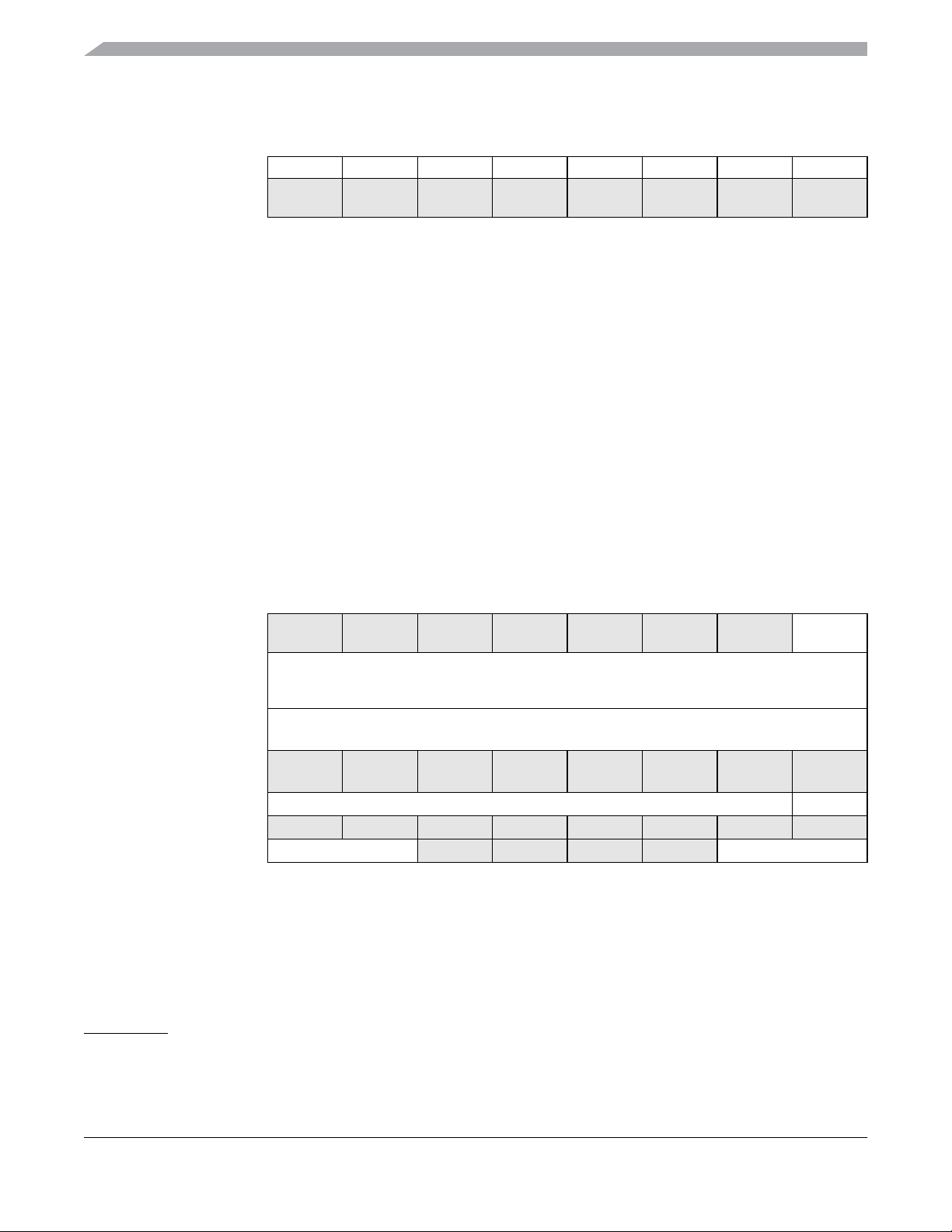
Chapter 4 Memory
Table 4-3. High-Page Register Summary (Sheet 4 of 4)
Address Register Name Bit 7 654321Bit 0
0x187D PTETOG PTETOG7 PTETOG6 PTETOG5 PTETOG4 PTETOG3 PTETOG2 PTETOG1 PTETOG0
0x187E–
0x187F
Reserved
—
—
—
—
—
—
—
—
—
—
—
—
—
—
—
—
Several reserved flash memory locations, shown in Table 4-4, are used for storing values used by several
registers.These registersinclude an 8-bytebackdoor key,NVBACKKEY, which can be used to gain access
to secure memory resources. During reset events, the contents of NVPROT and NVOPT in the reserved
flash memory are transferred into corresponding FPROT and FOPT registers in the high-page registers
area to control security and block protection options.
1
The factory ICS trim value is stored in the flash information row (IFR
) and will be loaded into the
ICSTRM and ICSSC registers after any reset. The internal reference trim values stored in flash, TRIM and
FTRIM, can be programmed by third party programmers and must be copied into the corresponding ICS
registers by user code to override the factory trim.
NOTE
When the MCU is in active BDM, the trim value in the IFR will not be
loaded. Instead, the ICSTRM register will reset to 0x80 and the FTRIM bit
in the ICSSC register will be reset to 0.
Table 4-4. Reserved Flash Memory Addresses
Address Register Name Bit 7 654321Bit 0
0xFFAE Reserved for
Storage of FTRIM
0xFFAF Reserved for
Storage of
ICSTRM
0xFFB0 –
NVBACKKEY
0xFFB7
0xFFB8 –
Reserved
0xFFBC
0xFFBD NVPROT
0xFFBE Reserved
0xFFBF NVOPT
0 0 0 0 0 0 0 FTRIM
TRIM
8-Byte Comparison Key
—
—
— — — — — — — —
KEYEN 0 0 0 0 SEC
—
—
—
—
—
—
FPS FPOPEN
—
—
—
—
—
—
—
—
Provided the key enable (KEYEN) bit is 1, the 8-byte comparison key can be used to temporarily
disengagememory security.Thiskey mechanism can be accessed only through user code running in secure
memory. (A security key cannot be entered directly through background debug commands.) This security
key can be disabled completely by programming the KEYEN bit to 0. If the security key is disabled, the
only way to disengage security is by mass erasing the flash if needed (normally through the background
1. IFR — Nonvolatile information memory that can be only accessed during production test. During production test, system
initialization, configuration and test information is stored in the IFR. This information cannot be read or modified in normal user
or background debug modes.
MC9S08QE128 MCU Series Reference Manual, Rev. 2
62 Freescale Semiconductor
Page 63

Chapter 4 Memory
(22-bits)
(4 MB)
from 64 basic, to 128K in MC9S08QE128
debug interface) and verifying that flash is blank. To avoid returning to secure mode after the next reset,
program the security bits (SEC) to the unsecured state (1:0).
4.4 Memory Management Unit
The memory management unit (MMU) allows the program and data space for the HCS08 Family of
microcontrollers to be extended beyond the 64K byte CPU addressable memory map. The MMU uses a
paging scheme similar to that seen on other MCU architectures, such as HCS12. The extended memory
when used for data can also be accessed linearly using a linear address pointer and data access registers.
4.4.1 Features
Key features of the MMU module are:
• Memory Management Unit extends the HCS08 memory space
— up to 4 MB for program and data space
• Extended program space using paging scheme
— PPAGE register used for page selection
— fixed 16K byte memory window
— architecture supports up to 256, 16K pages
• Extended data space using linear address pointer
— up to 22-bit linear address pointer
— linear address pointer and data register provided in direct page allows access of complete flash
memory map using direct page instructions
— optional auto increment of pointer when data accessed
— supports an 2s compliment addition/subtraction to address pointer without using any math
instructions or memory resources
— supports word accesses to any address specified by the linear address pointer when using
LDHX, STHX instructions
4.4.2 Register Definition
4.4.2.1 Program Page Register (PPAGE)
The HCS08 Core architecture limits the CPU addressable space availableto 64K bytes. The address space
can be extended to 128K bytes using a paging window scheme. The Program Page (PPAGE) allows for
selecting one of the 16K byte blocks to be accessed through the Program Page Window located at
0x8000-0xBFFF. The CALL and RTC instructions can load or store the value of PPAGE onto or from the
stack during program execution. After any reset, PPAGE is set to PAGE 2.
MC9S08QE128 MCU Series Reference Manual, Rev. 2
Freescale Semiconductor 63
Page 64
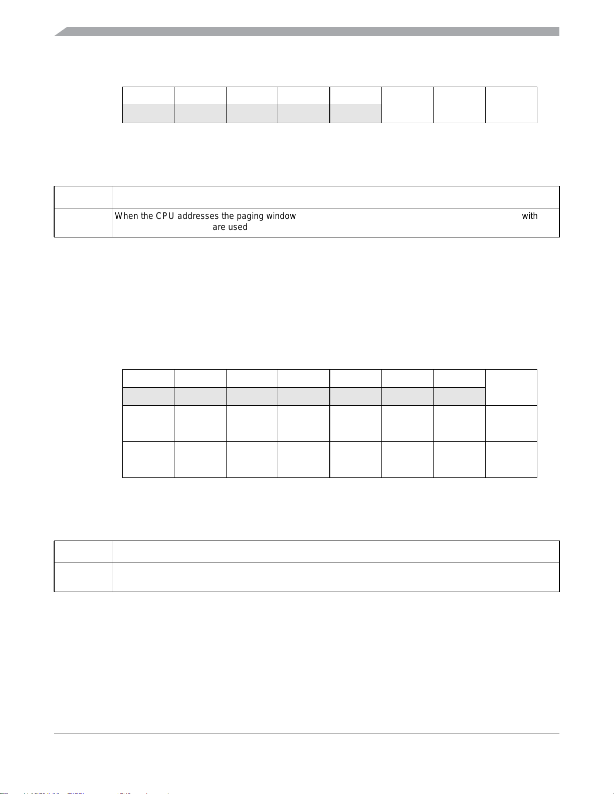
Chapter 4 Memory
76543210
R00000
W
Reset: 0 0 0 0 0 0 1 0
Figure 4-4. Program Page Register (PPAGE)
Table 4-5. Program Page Register Field Descriptions
Field Description
XA16 XA15 XA14
2:0
XA16:XA14
When the CPU addresses the paging window, 0x8000-0xBFFF, the value in the PPAGE register along with the
CPU addresses A13:A0 are used to create a 17-bit extended address.
4.4.2.2 Linear Address Pointer Registers 2:0 (LAP2:LAP0)
The three registers, LAP2:LAP0 contain the 17-bit linear address that allows the user to access any flash
location in the extended address map. This register is used in conjunction with the data registers, linear
byte (LB), linear byte post increment (LBP) and linear word post increment (LWP). The contents of
LAP2:LAP0 will auto-increment when accessing data using the LBP and LWP registers. The contents of
LAP2:LAP0 can be increased by writing an 8-bit value to LAPAB.
76543210
R0000000
W
R
LA15 LA14 LA13 LA12 LA11 LA10 LA9 LA8
W
R
LA7 LA6 LA5 LA4 LA3 LA2 LA1 LA0
W
Reset: 0 0 0 0 0 0 0 0
Figure 4-5. Linear Address Pointer Registers 2:0 (LAP2:LAP0)
LA16
Table 4-6. Linear Address Pointer Registers 2:0 Field Descriptions
Field Description
16:0
LA21:LA0
Thevaluesin LAP2:LAP0 are usedto create a 17-bit linear address pointer.The value in these registersare used
as the extended address when accessing any of the data registers LB, LBP and LWP.
4.4.2.3 Linear Word Post Increment Register (LWP)
This register is one of three data registers that the user can use to access any flash memory location in the
extended address map. When LWP is accessed the contents of LAP2:LAP0 make up the extended address
of the flash memory location to be addressed. When accessing data using LWP, the contents of
LAP2:LAP0 will increment after the read or write is complete.
MC9S08QE128 MCU Series Reference Manual, Rev. 2
64 Freescale Semiconductor
Page 65
Chapter 4 Memory
Accessing LWP does the same thing as accessing LBP. The MMU register ordering of LWP followed by
LBP, allow the user to access data by words using the LDHX or STHX instructions of the LWP register.
76543210
R
W
Reset: 0 0 0 0 0 0 0 0
Field Description
D7 D6 D5 D4 D3 D2 D1 D0
Figure 4-6. Linear Word Post Increment Register (LWP)
Table 4-7. Linear Word Post Increment Register Field Descriptions
7:0
D7:D0
Reads of this register will first return the data valuepointed to bythe linear address pointer, LAP2:LAP0 and then
will increment LAP2:LAP0. Writes to this register will first write the data value to the memory location specified
bythelinear address pointer and then will incrementLAP2:LAP0. Writes tothis register are mostcommonly used
when writing to the flash block(s) during programming.
4.4.2.4 Linear Byte Post Increment Register (LBP)
This register is one of three data registers that the user can use to access any flash memory location in the
extended address map. When LBP is accessed the contents of LAP2:LAP0 make up the extended address
of the flash memory locationto be addressed. Whenaccessing data using LBP, thecontents of LAP2:LAP0
will increment after the read or write is complete.
Accessing LBP does the same thing as accessing LWP. The MMU register ordering of LWP followed by
LBP, allow the user to access data by words using the LDHX or STHX instructions with the address of the
LWP register.
76543210
R
W
Reset: 0 0 0 0 0 0 0 0
D7 D6 D5 D4 D3 D2 D1 D0
Figure 4-7. Linear Byte Post Increment Register (LBP)
Table 4-8. Linear Byte Post Increment Register Field Descriptions
Field Description
7:0
D7:D0
Freescale Semiconductor 65
Reads of this register will first return the data valuepointed to bythe linear address pointer, LAP2:LAP0 and then
will increment LAP2:LAP0. Writes to this register will first write the data value to the memory location specified
bythelinear address pointer and then will incrementLAP2:LAP0. Writes tothis register are mostcommonly used
when writing to the flash block(s) during programming.
MC9S08QE128 MCU Series Reference Manual, Rev. 2
Page 66
Chapter 4 Memory
4.4.2.5 Linear Byte Register (LB)
This register is one of three data registers that the user can use to access any flash memory location in the
extended address map. When LB is accessed the contents of LAP2:LAP0 make up the extended address
of the flash memory location to be addressed.
76543210
R
W
Reset: 0 0 0 0 0 0 0 0
Field Description
D7 D6 D5 D4 D3 D2 D1 D0
Figure 4-8. Linear Byte Register (LB)
Table 4-9. Linear Data Register Field Descriptions
7:0
D7:D0
Reads of this register returns the data value pointed to by the linear address pointer,LAP2:LAP0. Writes to this
register will write the data value to the memory location specified by the linear address pointer. Writes to this
register are most commonly used when writing to the flash block(s) during programming.
4.4.2.6 Linear Address Pointer Add Byte Register (LAPAB)
The user can increase or decrease the contents of LAP2:LAP0 by writing a 2s compliment value to
LAPAB. The value written will be added to the current contents of LAP2:LAP0.
76543210
R00000000
WD7D6D5D4D3D2D1D0
Reset: 0 0 0 0 0 0 0 0
Figure 4-9. Linear Address Pointer Add Byte Register (LAPAB)
Table 4-10. Linear Address Pointer Add Byte Register Field Descriptions
Field Description
7:0
D7:D0
The 2s compliment value written to LAPAB will be added to contents of the linear address pointer register,
LAP2:LAP0. Writing a value of 0x7f to LAPAB will increase LAP by 127, a value of 0xff will decrease LAP by 1,
and a value of 0x80 will decrease LAP by 128.
4.4.3 Functional Description
4.4.3.1 Memory Expansion
The HCS08 Core architecture limits the CPU addressable space available to 64K bytes. The Program Page
(PPAGE) allows for integrating up to 4M byte of flash into the system by selecting one of the 16K byte
blocks to be accessed through the paging window located at 0x8000-0xBFFF. The MMU module also
provides a linear address pointer that allows extension of data access up to 4M bytes.
MC9S08QE128 MCU Series Reference Manual, Rev. 2
66 Freescale Semiconductor
Page 67

Chapter 4 Memory
4.4.3.1.1 Program Space
The PPAGE register holds the page select value for the paging window. The value in PPAGE can be
manipulated by using normal read and write instructions as well as the CALL and RTC instructions. The
user should not change PPAGE directly when running from paged memory, only CALL and RTC should
be used.
When the MMU detects that the CPU is addressing the paging window, the value currently in PPAGE will
be used to create an extended address that the MCU’s decode logic will use to select the desired flash
location.
As seen in Figure 4-1, the flash blocks in the CPU addressable memory can be accessed directly or using
the paging window and PPAGE register. For example, the flash from location 0x4000-0x7FFF can be
accessed directly or using the paging window, PPAGE = 1, address 0x8000-0xBFFF.
4.4.3.1.2 CALL and RTC (Return from Call) Instructions
CALL and RTC are instructions that perform automated page switching when executed in the user
program. CALL is similar to a JSR instruction, but the subroutine that is called can be located anywhere
in the normal 64K byte address space or on any page of program memory.
During the execution of a CALL instruction, the CPU:
• Stacks the return address.
• Pushes the current PPAGE value onto the stack.
• Writes the new instruction-supplied PPAGE value into the PPAGE register.
• Transfers control to the subroutine of the new instruction-supplied address.
This sequence is not interruptible; there is no need to inhibit interrupts during CALL execution. A CALL
can be executed from any address in memory to any other address.
The new PPAGE value is provided by an immediate operand in the instruction along with the address
within the paging window, 0x8000-0xBFFF.
RTC is similar to an RTS instruction.
The RTC instruction terminates subroutines invoked by a CALL instruction.
During the execution of an RTC instruction, the CPU:
• Pulls the old PPAGE value from the stack and loads it into the PPAGE register
• Pulls the 16-bit return address from the stack and loads it into the PC
• Resumes execution at the return address
This sequence is not interruptible; there is no need to inhibit interrupts during RTC execution. An RTC
can be executed from any address in memory.
MC9S08QE128 MCU Series Reference Manual, Rev. 2
Freescale Semiconductor 67
Page 68

Chapter 4 Memory
4.4.3.1.3 Data Space
The linear address pointer registers, LAP2:LAP0 along with the linear data register allow the CPU to read
or write any address in the extended flash memory space. This linear address pointer may be used to access
data from any memory location while executing code from any location in extended memory, including
accessing data from a different PPAGE than the currently executing program.
To access data using the linear address pointer, the user would first setup the extended address in the 22-bit
address pointer, LAP2:LAP0. Accessing one of the three linear data registers LB, LBP and LWP will
access the extended memory location specified by LAP2:LAP0. The three linear data registers access the
memory locations in the same way, however the LBP and LWP will also increment LAP2:LAP0.
Accessing either the LBP or LWP registers allows a user program to read successive memory locations
without re-writing the linear address pointer. Accessing LBP or LWP does the exact same function.
However, because of the address mapping of the registers with LBP following LWP, a user can do word
accesses in the extended address space using the LDHX or STHX instructions to access location LWP.
The MMU supports the addition of a 2s compliment value to the linear address pointer without using any
math instructions or memory resources. Writes to LAPAB with a 2s compliment value will cause the
MMU to add that value to the existing value in LAP2:LAP0.
4.4.3.1.4 PPAGE and Linear Address Pointer to Extended Address
See Figure 4-1, on how the program PPAGEmemory pages and the Linear Address Pointer are mapped to
extended address space.
MC9S08QE128 MCU Series Reference Manual, Rev. 2
68 Freescale Semiconductor
Page 69

Chapter 4 Memory
MMU
4.5 RAM
The MC9S08QE128 Series includes static RAM. The locations in RAM below 0x0100 can be accessed
using the more efficient direct addressing mode, and any single bit in this area can be accessed with the bit
manipulation instructions (BCLR, BSET, BRCLR, and BRSET). Locating the most frequently accessed
program variables in this area of RAM is preferred.
At power-on, the contents of RAM are uninitialized. RAM data is unaffected by any reset provided that
the supply voltage does not drop below the minimum value for RAM retention (V
For compatibility with M68HC05 MCUs, the HCS08 resets the stack pointer to 0x00FF. In the
MC9S08QE128 Series, it is usually best to reinitialize the stack pointer to the top of the RAM so the direct
page RAM can be used for frequently accessed RAM variables and bit-addressable program variables.
Include the following 2-instruction sequence in your resetinitialization routine (where RamLast is equated
to the highest address of the RAM in the Freescale Semiconductor-provided equate file).
LDHX #RamLast+1 ;point one past RAM
TXS ;SP<-(H:X-1)
When security is enabled, the RAM is considered a secure memory resource and is not accessible through
BDM or through code executing from non-secure memory. See Section 4.6.5, “Flash Module Security,”
for a detailed description of the security feature.
RAM
).
4.6 Flash
The flash memory is intended primarily for program storage. In-circuit programming allows the operating
program to be loaded into the flash memory after final assembly of the application product. It is possible
to program the entire array through the single-wire background debug interface. Because no special
voltages are needed for flash erase and programming operations, in-application programming is also
possible through other software-controlled communication paths.
The flash memory is ideal for single-supply applications allowing for field reprogramming without
requiring external high voltage sources for program or erase operations. The flash module includes a
memory controller that executes commands to modify flash memory contents.
Array read access time isone bus cycle per byte. For flash memory, anerased bit reads 1 and a programmed
bit reads 0. It is not possible to read from a flash block while any command is executing on that specific
flash block. It is possible to read from a flash block while a command is executing on a different flash
block.
CAUTION
A flash block address must be in the erased state before being programmed.
Cumulativeprogramming of bits within a flash block address is not allowed
except for status field updates required in EEPROM emulation applications.
For a more detailed discussion of in-circuit and in-application programming, refer to the HCS08 Family
Reference Manual, Volume I, Freescale Semiconductor document order number HCS08RMv1.
MC9S08QE128 MCU Series Reference Manual, Rev. 2
Freescale Semiconductor 69
Page 70

Chapter 4 Memory
4.6.1 Features
Features of the flash memory include:
• Flash size
— MC9S08QE128: 131,072 bytes (256 pages of 512 bytes each)
— MC9S08QE96: 98,304 bytes (192 pages of 512 bytes each)
— MC9S08QE64: 65,536 bytes (128 pages of 512 bytes each)
• Single power supply program and erase
• Automated program and erase algorithm
• Fast program and erase operation
• Burst program command for faster flash array program times
• Up to 100,000 program/erase cycles at typical voltage and temperature
• Flexible protection scheme to prevent accidental program or erase
• Security feature to prevent unauthorized access to the flash and RAM
• Auto power-down for low-frequency read accesses
4.6.2 Register Descriptions
The flash module contains a set of 16 control and status registers. Detailed descriptions of each register bit
are provided in the following sections.
4.6.2.1 Flash Clock Divider Register (FCDIV)
The FCDIV registeris used to control the length of timed eventsin program and erase algorithms executed
by the flash memory controller.
76543210
R
FDIVLD PRDIV8 FDIV
W
Reset 00000000
Figure 4-10. Flash Clock Divider Register (FCDIV)
All bits in the FCDIV register are readable and writable with restrictions as determined by the value of
FDIVLD when writing to the FCDIV register (see Table 4-11).
MC9S08QE128 MCU Series Reference Manual, Rev. 2
70 Freescale Semiconductor
Page 71
Table 4-11. FCDIV Field Descriptions
Field Description
Chapter 4 Memory
7
FDIVLD
6
PRDIV8
5:0
FDIV[5:0]
Clock Divider Load Control — When writing to the FCDIV register for the first time after a reset, the value of
the FDIVLD bit written controls the future ability to write to the FCDIV register:
0 Writing a 0 to FDIVLD locks the FCDIV register contents; all future writes to FCDIV are ignored.
1 Writing a 1 to FDIVLD keeps the FCDIV register writable; next write to FCDIV is allowed.
When reading the FCDIV register, the value of the FDIVLD bit read indicates the following:
0 FCDIV register has not been written to since the last reset.
1 FCDIV register has been written to since the last reset.
Enable Prescaler by 8
0 The bus clock is directly fed into the clock divider.
1 The bus clock is divided by 8 before feeding into the clock divider.
Clock Divider Bits — The combination of PRDIV8 and FDIV[5:0] must divide the bus clockdown to a frequency
of 150 kHz–200 kHz. The minimum divide ratio is 2 and the maximum divide ratio is 512. Please referto Section
4.6.3.1.1, “Writing the FCDIV Register” for more information.
.
if PRDIV8 = 0 — f
if PRDIV8 = 1 — f
FCLK
FCLK
= f
= f
÷ (DIV + 1) Eqn. 4-1
Bus
÷ (8 × (DIV + 1)) Eqn. 4-2
Bus
Table 4-12 shows the appropriate values for PRDIV8 and DIV for selected bus frequencies.
Table 4-12. Flash Clock Divider Settings
f
Bus
PRDIV8
(Binary)
DIV
(Decimal)
f
FCLK
Program/Erase Timing Pulse
(5 μs Min, 6.7 μs Max)
20 MHz 1 12 192.3 kHz 5.2 μs
10 MHz 0 49 200 kHz 5 μs
8 MHz 0 39 200 kHz 5 μs
4 MHz 0 19 200 kHz 5 μs
2 MHz 0 9 200 kHz 5 μs
1 MHz 0 4 200 kHz 5 μs
200 kHz 0 0 200 kHz 5 μs
150 kHz 0 0 150 kHz 6.7 μs
4.6.2.2 Flash Options Register (FOPT and NVOPT)
The FOPT register holds all bits associated with the security of the MCU and flash module.
76543210
R KEYEN 0 0 0 0 SEC
W
Reset F F 0 0 0 0 F F
= Unimplemented or Reserved
Figure 4-11. Flash Options Register (FOPT)
MC9S08QE128 MCU Series Reference Manual, Rev. 2
Freescale Semiconductor 71
Page 72
Chapter 4 Memory
All bits in the FOPT register are readable but are not writable. To change the value in this register, erase
and reprogram the NVOPT location in flash memory as usual and then issue an MCU reset.
The FOPT register is loaded from the flash location, NVOPT, during the reset sequence, indicated by F in
Figure 4-11.
Table 4-13. FOPT Field Descriptions
Field Description
7:6
KEYEN[1:0]
1:0
SEC[1:0]
Backdoor Key Security Enable Bits — The KEYEN[1:0] bits define the enabling of backdoor keyaccess to the
flash module as shown in Table 4-14.
Flash Security Bits — The SEC[1:0] bits define the security state of the MCU as shown in Table 4-15. If the
flash module is unsecured using backdoor key access, the SEC[1:0] bits are forced to the unsecured state.
Table 4-14. Flash KEYEN States
KEYEN[1:0] Status of Backdoor Key Access
00 DISABLED
1
01
10 ENABLED
11 DISABLED
1
Preferred KEYEN state to disable Backdoor Key Access.
DISABLED
Table 4-15. Flash Security States
SEC[1:0] Status of Security
00 SECURED
1
01
10 UNSECURED
11 SECURED
1
Preferred SEC state to set MCU to secured state.
SECURED
The security feature in the flash module is described in Section 4.6.5, “Flash Module Security”.
4.6.2.3 Flash Configuration Register (FCNFG)
The FCNFG register enables the flash interrupts and gates the security backdoor writes.
76543210
R0 0
KEYACC
W
Reset 00000000
= Unimplemented or Reserved
Figure 4-12. Flash Configuration Register (FCNFG)
MC9S08QE128 MCU Series Reference Manual, Rev. 2
72 Freescale Semiconductor
00000
Page 73

Chapter 4 Memory
CBEIE, CCIE and KEYACC bits are readable and writable while all remaining bits read 0 and are not
writable. KEYACC is only writable if KEYEN is set to the enabled state (see Section 4.6.2.2, “Flash
Options Register (FOPT and NVOPT)”.
Table 4-16. FCNFG Field Descriptions
Field Description
5
KEYACC
Enable Security Key Writing
0 Writes to the flash block are interpreted as the start of a command write sequence.
1 Writes to the flash block are interpreted as keys to open the backdoor.
NOTE
Flash array reads are allowed while KEYACC is set.
4.6.2.4 Flash Protection Register (FPROT and NVPROT)
The FPROT register defines which flash sectors are protected against program or erase operations.
76543210
R
W
Reset F F FFFFFF
Figure 4-13. Flash Protection Register (FPROT)
FPROT bits are readable and writable as long as the size of the protected flash memory is being increased.
Any write to FPROT that attempts to decrease the size of the protected flash memory will be ignored.
During the reset sequence, the FPROT register is loaded from the flash protection byte, NVPROT. To
change the flash protection that will be loaded during the reset sequence, the flash sector containing
NVPROT must be unprotected and erased, then NVPROT can be reprogrammed.
FPS FPOPEN
Tryingto alter data in any protected area in the flash memory will result in a protection violation error and
the FPVIOL flag will be set in the FSTAT register. The mass erase of the flash array is not possible if any
of the flash sectors contained in the flash array are protected.
Table 4-17. FPROT Field Descriptions
Field Description
7:1
FPS[6:0]
0
FPOPEN
Freescale Semiconductor 73
Flash Protection Size — With FPOPEN set, the FPS bits determine the size of the protected flash address
range as shown in Table4-18.
Flash Protection Open
0 Flash array fully protected.
1 Flash array protected address range determined by FPS bits.
MC9S08QE128 MCU Series Reference Manual, Rev. 2
Page 74
Chapter 4 Memory
Table 4-18. Flash Protection Address Range
Protected Address Range
FPS[6:0] FPOPEN
- 0 0x0_0000–0x0_FFFF 0x1_0000–0x1_FFFF 128 Kbytes
0x00 1 0x0_0000–0x0_FFFF 0x1_0400–0x1_FFFF 127 Kbytes
0x01 0x0_0000–0x0_FFFF 0x1_0800–0x1_FFFF 126 Kbytes
0x02 0x0_0000–0x0_FFFF 0x1_0C00–0x1_FFFF 125 Kbytes
0x03 0x0_0000–0x0_FFFF 0x1_1000–0x1_FFFF 124 Kbytes
0x04 0x0_0000–0x0_FFFF 0x1_1400–0x1_FFFF 123 Kbytes
0x05 0x0_0000–0x0_FFFF 0x1_1800–0x1_FFFF 122 Kbytes
0x06 0x0_0000–0x0_FFFF 0x1_1C00–0x1_FFFF 121 Kbytes
... ... ... ...
0x37 0x0_0000–0x0_FFFF 0x1_E000–0x1_FFFF 72 Kbytes
0x38 0x0_0000–0x0_FFFF 0x1_E400–0x1_FFFF 71 Kbytes
0x39 0x0_0000–0x0_FFFF 0x1_E800–0x1_FFFF 70 Kbytes
0x3A 0x0_0000–0x0_FFFF 0x1_EC00–0x1_FFFF 69 Kbytes
0x3B 0x0_0000–0x0_FFFF 0x1_F000–0x1_FFFF 68 Kbytes
0x3C 0x0_0000–0x0_FFFF 0x1_F400–0x1_FFFF 67 Kbytes
0x3D 0x0_0000–0x0_FFFF 0x1_F800–0x1_FFFF 66 Kbytes
0x3E 0x0_0000–0x0_FFFF 0x1_FC00–0x1_FFFF 65 Kbytes
0x3F 0x0_0000–0x0_FFFF 64 Kbytes
0x40 0x0_0400–0x0_FFFF 63 Kbytes
0x41 0x0_0800–0x0_FFFF 62 Kbytes
0x42 0x0_0C00–0x0_FFFF 61 Kbytes
0x43 0x0_1000–0x0_FFFF 60 Kbytes
0x44 0x0_1400–0x0_FFFF 59 Kbytes
0x45 0x0_1800–0x0_FFFF 58 Kbytes
0x46 0x0_1C00–0x0_FFFF 57 Kbytes
... ... ...
0x77 0x0_E000–0x0_FFFF 8 Kbytes
0x78 0x0_E400–0x0_FFFF 7 Kbytes
0x79 0x0_E800–0x0_FFFF 6 Kbytes
0x7A 0x0_EC00–0x0_FFFF 5 Kbytes
0x7B 0x0_F000–0x0_FFFF 4 Kbytes
0x7C 0x0_F400–0x0_FFFF 3 Kbytes
0x7D 0x0_F800–0x0_FFFF 2 Kbytes
0x7E 0x0_FC00–0x0_FFFF 1 Kbyte
0x7F No Protection 0 Kbytes
Relative to Flash Array Base
Flash Array 0 Flash Array 1
Protected
Size
MC9S08QE128 MCU Series Reference Manual, Rev. 2
74 Freescale Semiconductor
Page 75

Chapter 4 Memory
4.6.2.5 Flash Status Register (FSTAT)
The FSTAT register defines the operational status of the flash module.
FCCF, FPVIOL, and FACCERR are readable and writable, FCCF and FBLANK are readable and not
76543210
R
FCBEF
W
Reset 11000000
writable, remaining bits read 0 and are not writable.
Field Description
FCCF
FPVIOL FACCERR
= Unimplemented or Reserved
Figure 4-14. Flash Status Register (FSTAT)
Table 4-19. FSTAT Field Descriptions
0 FBLANK 0 0
7
FCBEF
6
FCCF
5
FPVIOL
Flash Command Buffer Empty Flag — The FCBEF flag indicates that the command buffer is empty so that a
new command write sequence can be started when performing burst programming. Writing a 0 to the FCBEF
flag has no effect on FCBEF. Writing a 0 to FCBEF after writing an aligned address to the flash array memory,
but before FCBEF is cleared, will abort a command write sequence and cause the FACCERR flag to be set.
Writing a 0 to FCBEF outside of a command write sequence will not set the FACCERR flag. The FCBEF flag is
cleared by writing a 1 to FCBEF.
0 Command buffers are full.
1 Command buffers are ready to accept a new command.
Flash Command Complete Interrupt Flag — The FCCF flag indicates that there are no more commands
pending. The FCCF flag is cleared when FCBEF is cleared and sets automatically upon completion of all active
and pending commands. The FCCF flag does not set when an active program command completes and a
pending burst program command is fetched from the command buffer. Writing to the FCCF flag has no effect on
FCCF.
0 Command in progress.
1 All commands are completed.
Flash Protection Violation Flag —The FPVIOL flag indicates an attempt was made to program or erase an
address in a protected area of the flash memory or flash IFR during a command write sequence. Writing a 0 to
the FPVIOL flag has no effect on FPVIOL. The FPVIOL flag is cleared by writing a 1 to FPVIOL. While FPVIOL
is set, it is not possible to launch a command or start a command write sequence.
0 No protection violation detected.
1 Protection violation has occurred.
MC9S08QE128 MCU Series Reference Manual, Rev. 2
Freescale Semiconductor 75
Page 76

Chapter 4 Memory
Table 4-19. FSTAT Field Descriptions
Field Description
4
FACCERR
2
FBLANK
Flash Access Error Flag — The FACCERR flag indicates an illegal access has occurred to the flash memory
or flash IFR caused by either a violation of the command write sequence (see Section 4.6.3.1.2, “Command
Write Sequence”), issuing an illegalflash command (see Table4-21), or the executionof a CPUSTOPinstruction
while a command is executing (FCCF = 0). Writing a 0 to the FACCERR flag has no effect on FACCERR. The
FACCERR flag is cleared by writing a 1 to FACCERR.While FACCERR is set, it is not possible to launch a
command or start a command write sequence.
0 No access error detected.
1 Access error has occurred.
Flash Flag Indicating the Erase Verify Operation Status — When the FCCF flag is set after completion of an
erase verify command, the FBLANK flag indicates the result of the erase verify operation. The FBLANK flag is
cleared by the flash module when FCBEF is cleared as part of a new valid command write sequence. Writing to
the FBLANK flag has no effect on FBLANK.
0 Flash block verified as not erased.
1 Flash block verified as erased.
4.6.2.6 Flash Command Register (FCMD)
The FCMD register is the flash command register.
76543210
R0
W
Reset 00000000
= Unimplemented or Reserved
FCMD
Figure 4-15. Flash Command Register (FCMD)
All FCMD bits are readable and writable during a command write sequence while bit 7 reads 0 and is not
writable.
Table 4-20. FCMD Field Descriptions
Field Description
6:0
FCMD[6:0]
Flash Command — Valid flash commands are shown inTable 4-21. Writing any command other than those
listed in Table 4-21 sets the FACCERR flag in the FSTAT register.
Table 4-21. Valid Flash Command List
FCMD[6:0] NVM Command
0x05 Erase Verify
0x20 Program
0x25 Burst Program
0x40 Sector Erase
0x41 Mass Erase
MC9S08QE128 MCU Series Reference Manual, Rev. 2
76 Freescale Semiconductor
Page 77
Chapter 4 Memory
4.6.3 Functional Description
4.6.3.1 Flash Command Operations
Flash command operations are used to execute program, erase, and erase verify algorithms described in
this section. The program and erase algorithms are controlled by the flash memory controller whose time
base, FCLK, is derived from the bus clock via a programmable divider.
The next sections describe:
1. How to write the FCDIV register to set FCLK
2. Command write sequences to program, erase, and erase verify operations on the flash memory
3. Valid flash commands
4. Effects resulting from illegal flash command write sequences or aborting flash operations
4.6.3.1.1 Writing the FCDIV Register
Prior to issuing any flash command after a reset, the user is required to write the FCDIV register to divide
the bus clock down to within the 150 kHz to 200 kHz range. This register can be written only once, so
normally this write is done during reset initialization. FCDIV cannot be written if the access error flag,
FACCERR in FSTAT, is set. The user must ensure that FACCERR is not set before writing to the FCDIV
register. One period of the resulting clock (1/f
anderase pulses. Aninteger number of these timing pulses are used by the command processor to complete
a program or erase command.
) is used by the command processor to time program
FCLK
Table 4-22 shows program and erase times. The bus clock frequency and FCDIV determine the frequency
of FCLK (f
). The time for one cycle of FCLK is t
FCLK
of cycles of FCLK and as an absolute time for the case where t
FCLK
= 1/f
FCLK
. The times are shown as a number
FCLK
=5μs. Program and erase times
shown include overhead for the command state machine and enabling and disabling of program and erase
voltages.
Table 4-22. Program and Erase Times
Parameter Cycles of FCLK Time if FCLK = 200 kHz
Byte program 9 45 μs
Byte program (burst) 4 20 μs
Page erase 4000 20ms
Mass erase 20,000 100 ms
1
Excluding start/end overhead
1
NOTE
Program and erase command execution time will increase proportionally
with the period of FCLK. Programming or erasing the flash memory with
FCLK < 150 kHz should be avoided. Setting FCDIV to a value such that
FCLK < 150 kHz can destroy the flash memory due to overstress. Setting
FCDIV to a value such that FCLK > 200 kHz can result in incomplete
programming or erasure of the flash memory cells.
MC9S08QE128 MCU Series Reference Manual, Rev. 2
Freescale Semiconductor 77
Page 78

Chapter 4 Memory
If the FCDIV register is written, the FDIVLD bit is set automatically. If the FDIVLD bit is 0, the FCDIV
register has not been written since the last reset. If the FCDIV register has not been written to, the flash
command loaded during a command write sequence will not execute and the FACCERRflag in the FSTAT
register will set.
4.6.3.1.2 Command Write Sequence
The flash command controller is used to supervise the command write sequence to executeprogram, erase,
and erase verify algorithms.
Before starting a command write sequence, the FACCERR and FPVIOL flags in the FSTAT register must
be clear and the FCBEF flag must be set (see Section 4.6.2.5).
Acommand write sequence consists of three stepswhich must be strictly adhered to withwrites to the flash
module not permitted between the steps. However, flash register and array reads are allowed during a
command write sequence. The basic command write sequence is as follows:
1. Write to a valid address in the flash array memory.
2. Write a valid command to the FCMD register.
3. Clear the FCBEF flag in the FSTAT register by writing a 1 to FCBEF to launch the command.
Once a command is launched, the completion of the command operation is indicated by the setting of the
FCCF flag in the FSTAT register. The FCCF flag will set upon completion of all active and buffered burst
program commands.
4.6.3.2 Flash Commands
Table 4-23 summarizes the valid flash commands along with the effects of the commands on the flash
block.
Table 4-23. Flash Command Description
FCMDB
0x05 Erase
0x20 Program Program an address in the flash array.
0x25 Burst
0x40 Sector
0x41 Mass
NVM
Command
Verify
Program
Erase
Erase
Verify all memory bytes in the flash array memory are erased.
If the flash array memory is erased, the FBLANK flag in the FSTATregister will set upon
command completion.
Program an address in the flash array with the internal address incrementing after the
program operation.
Erase all memory bytes in a sector of the flash array.
Erase all memory bytes in the flash array.
A mass erase of the full flash array is only possible when no protection is enabled prior
to launching the command.
Function on Flash Memory
CAUTION
A flash block address must be in the erased state before being programmed.
Cumulativeprogramming of bits within a flash block address is not allowed
except for status field updates required in EEPROM emulation applications.
MC9S08QE128 MCU Series Reference Manual, Rev. 2
78 Freescale Semiconductor
Page 79

Chapter 4 Memory
4.6.3.2.1 Erase Verify Command
The erase verify operation will verify that a flash block is erased.
An example flow to execute the erase verify operation is shownin Figure 4-16. The erase verify command
write sequence is as follows:
1. Write to a flash block address to start the command write sequence for the erase verify command.
The address and data written will be ignored.
2. Write the erase verify command, 0x05, to the FCMD register.
3. Clear the FCBEF flag in the FSTAT register by writing a 1 to FCBEF to launch the erase verify
command.
After launching the erase verify command, the FCCF flag in the FSTAT register will set after the operation
has completed. The number of bus cycles required to execute the erase verify operation is equal to the
number of addresses in the flash array memory plus several bus cycles as measured from the time the
FCBEF flag is cleared until the FCCF flag is set. Upon completion of the erase verify operation, the
FBLANK flag in the FSTAT register will be set if all addresses in the flash array memory are verified to
be erased. If any address in the flash array memory is not erased, the erase verify operation will terminate
and the FBLANK flag in the FSTAT register will remain clear.
MC9S08QE128 MCU Series Reference Manual, Rev. 2
Freescale Semiconductor 79
Page 80
Chapter 4 Memory
START
Read: FCDIV register
Clock Register
Written
Check
Command
Buffer Empty Check
Access Error and
Protection Violation
Check
Bit Polling for
Command Completion
Check
FDIVLD
Set?
yes
Read: FSTAT register
FCBEF
yes
FACCERR/FPVIOL
no
Write: Flash Block Address
1.
and Dummy Data
Write: FCMD register
2.
Erase Verify Command 0x05
Write: FSTAT register
3.
Clear FCBEF 0x80
Read: FSTAT register
FCCF
yes
no
Write: FCDIV register
no
Set?
yes
Set?
no
Set?
NOTE: FCDIV needs to
be set after each reset
Write: FSTAT register
Clear FACCERR/FPVIOL 0x30
Erase Verify
Status
FBLANK
Set?
yes
EXIT
no
Flash Block
Erased
EXIT
Flash Block
Not Erased
Figure 4-16. Example Erase Verify Command Flow
4.6.3.2.2 Program Command
The program operation will program a previously erased address in the flash memory using an embedded
algorithm.
An example flow to execute the program operation is shown in Figure 4-17. The program command write
sequence is as follows:
1. Write to a flash block address to start the command write sequence for the program command. The
data written will be programmed to the address written.
2. Write the program command, 0x20, to the FCMD register.
MC9S08QE128 MCU Series Reference Manual, Rev. 2
80 Freescale Semiconductor
Page 81
Chapter 4 Memory
3. Clear the FCBEF flag in the FSTAT register by writing a 1 to FCBEF to launch the program
command.
If an address to be programmed is in a protected area of the flash block, the FPVIOL flag in the FSTAT
register will set and the program command will not launch. Once the program command has successfully
launched, the FCCF flag in the FSTAT register will set after the program operation has completed.
START
Read: FCDIV register
Clock Register
Written
Check
Command
Buffer Empty Check
Access Error and
Protection Violation
Check
Bit Polling for
Command Completion
Check
FDIVLD
Set?
yes
Read: FSTAT register
yes
FACCERR/FPVIOL
Write: Flash Array Address
1.
and Program Data
Write: FCMD register
2.
Program Command 0x20
Write: FSTAT register
3.
Clear FCBEF 0x80
Read: FSTAT register
no
Write: FCDIV register
FCBEF
Set?
Set?
no
FCCF
Set?
yes
EXIT
no
yes
no
NOTE: FCDIV needs to
be set after each reset
Write: FSTAT register
Clear FACCERR/FPVIOL 0x30
Figure 4-17. Example Program Command Flow
4.6.3.2.3 Burst Program Command
The burst program operation will program previously erased data in the flash memory using an embedded
algorithm.
While burst programming, two internal data registers operate as a buffer and a register (2-stage FIFO) so
that a second burst programming command along with the necessary data can be storedto the bufferswhile
the first burst programming command is still in progress. This pipelined operation allows a time
MC9S08QE128 MCU Series Reference Manual, Rev. 2
Freescale Semiconductor 81
Page 82

Chapter 4 Memory
optimization when programming more than one consecutive address on a specific row in the flash array as
the high voltage generation can be kept active in between two programming commands.
An example flow to execute the burst program operation is shown in Figure 4-18. The burst program
command write sequence is as follows:
1. Writeto a flashblock address to start the command write sequence for the burst program command.
The data written will be programmed to the address written.
2. Write the program burst command, 0x25, to the FCMD register.
3. Clear the FCBEF flag in the FSTAT register by writing a 1 to FCBEF to launch the program burst
command.
4. After the FCBEF flag in the FSTAT register returns to a 1, repeat steps 1 through 3. The address
written is ignored but is incremented internally.
The burst program procedure can be used to program an entire flash array even while crossing row
boundaries within the flash array. However, the burst program command cannot cross array boundaries.
The array boundary for this MCU occurs between extended addresses 0x0FFFF and 0x10000. At least two
burst commands are required to program the entire 128K of flash memory.
If data to be burst programmed falls within a protected area of the flash array, the FPVIOL flag in the
FSTAT register will set and the burstprogram command will notlaunch. Once the burstprogram command
has successfully launched, the FCCF flag in the FSTAT register will set after the burst program operation
has completed unless a new burst program command write sequence has been buffered. By executing a
new burst program command write sequence on sequential addresses after the FCBEF flag in the FSTAT
registerhas been set, greater than 50% faster programming time for the entire flash array can be effectively
achieved when compared to using the basic program command.
MC9S08QE128 MCU Series Reference Manual, Rev. 2
82 Freescale Semiconductor
Page 83
START
Read: FCDIV register
Chapter 4 Memory
Clock Register
Written
Check
Command
Buffer Empty Check
Access Error and
Protection Violation
Check
1.
2.
3.
Bit Polling for
Command Buffer Empty
Check
Sequential
Programming
Decision
FDIVLD
Set?
yes
Read: FSTAT register
FACCERR/FPVIOL
Write: Flash Array Address
and Program Data
Write: FCMD register
Burst Program Command 0x25
Write: FSTAT register
Clear FCBEF 0x80
Read: FSTAT register
Read: FSTAT register
no
Write: FCDIV register
FCBEF
Set?
yes
Set?
no
FCBEF
Set?
yes
Next
Address?
no
no
yes
no
yes
NOTE: FCDIV needs to
be set after each reset
Write: FSTAT register
Clear FACCERR/FPVIOL 0x30
Bit Polling for
Command Completion
Check
FCCF
Set?
yes
EXIT
no
Figure 4-18. Example Burst Program Command Flow
4.6.3.2.4 Sector Erase Command
The sector erase operation will erase all addresses in a 1 Kbyte sector of flash memory using an embedded
algorithm.
MC9S08QE128 MCU Series Reference Manual, Rev. 2
Freescale Semiconductor 83
Page 84
Chapter 4 Memory
An example flowto execute the sector erase operation is shown in Figure 4-19. The sector erase command
write sequence is as follows:
1. Write to a flash block address to start the command write sequence for the sector erase command.
The flash address written determines the sector to be erased while global address bits [8:0] and the
data written are ignored.
2. Write the sector erase command, 0x40, to the FCMD register.
3. Clear the FCBEF flag in the FSTAT register by writing a 1 to FCBEF to launch the sector erase
command.
If a flash sector to be erased is in a protected area of the flash block, the FPVIOL flag in the FSTAT register
will set and the sector erase command will not launch. Once the sector erase command has successfully
launched, the FCCF flag in the FSTAT register will set after the sector erase operation has completed.
START
Read: FCDIV register
Clock Register
Written
Check
Command
Buffer Empty Check
Access Error and
Protection Violation
Check
Bit Polling for
Command Completion
Check
FDIVLD
Set?
yes
Write: Flash Sector Address
1.
and Dummy Data
Write: FCMD register
2.
Sector Erase Command 0x40
Write: FSTAT register
3.
Clear FCBEF 0x80
Write: FCDIV register
Read: FSTAT register
FCBEF
Set?
yes
FACCERR/FPVIOL
Set?
no
Read: FSTAT register
FCCF
Set?
yes
EXIT
no
no
yes
no
NOTE: FCDIV needs to
be set after each reset
Write: FSTAT register
Clear FACCERR/FPVIOL 0x30
Figure 4-19. Example Sector Erase Command Flow
MC9S08QE128 MCU Series Reference Manual, Rev. 2
84 Freescale Semiconductor
Page 85

Chapter 4 Memory
4.6.3.3 Illegal Flash Operations
4.6.3.3.1 Flash Access Violations
The FACCERR flag will be set during the command write sequence if any of the following illegal steps
are performed, causing the command write sequence to immediately abort:
1. Writing to a flash address before initializing the FCDIV register.
2. Writing to any flash register other than FCMD after writing to a flash address.
3. Writing to a second flash address in the same command write sequence.
4. Writing an invalid command to the FCMD register unless the address written was in a protected
area of the flash array.
5. Writing a command other than burst program while FCBEF is set and FCCF is clear.
6. When security is enabled, writing a command other than mass erase to the FCMD register when
the write originates from a non-secure memory location or from the background debug mode.
7. Writing to a flash address after writing to the FCMD register.
8. Writing to any flash registerother than FSTAT (to clear FCBEF) after writing to the FCMD register.
9. Writing a 0 to the FCBEF flag in the FSTAT register to abort a command write sequence.
The FACCERR flag will also be set if the MCU enters stop mode while a program or erase operation is
active. The operation is aborted immediately and, if burst programming, any pending burst program
command is purged (see Section 4.6.4.2, “Stop Mode”).
The FACCERR flag will not be set if any flash register is read during a valid command write sequence.
If the flash memory is read during execution of an algorithm (FCCF = 0), the read operation will return
invalid data and the FACCERR flag will not be set.
If the FACCERR flag is set in the FSTAT register, the user must clear the FACCERR flag before starting
another command write sequence (see Section 4.6.2.5, “Flash Status Register (FSTAT)”).
4.6.3.3.2 Flash Protection Violations
The FPVIOL flag will be set after the command is written to the FCMD register during a command write
sequence if any of the following illegal operations are attempted, causing the command write sequence to
immediately abort:
1. Writing the program command if the address written in the command write sequence was in a
protected area of the flash array.
2. Writing the sector erase command if the address written in the command write sequence was in a
protected area of the flash array.
3. Writing the mass erase command while any flash protection is enabled.
4. Writing an invalid command if the address written in the command write sequence was in a
protected area of the flash array.
If the FPVIOL flag is set in the FSTAT register,the user must clear the FPVIOL flag before starting another
command write sequence (see Section 4.6.2.5, “Flash Status Register (FSTAT)”).
MC9S08QE128 MCU Series Reference Manual, Rev. 2
Freescale Semiconductor 85
Page 86

Chapter 4 Memory
4.6.4 Operating Modes
4.6.4.1 Wait Mode
If a command is active(FCCF = 0) when the MCU enters wait mode, the active command and any buffered
command will be completed.
4.6.4.2 Stop Mode
If a command is active (FCCF = 0) when the MCU enters stop mode, the operation will be aborted and, if
the operation is program or erase, the flash array data being programmed or erased may be corrupted and
the FCCF and FACCERR flags will be set. If active, the high voltage circuitry to the flash array will
immediately be switched off when entering stop mode. Upon exit from stop mode, the FCBEF flag is set
and any buffered command will not be launched. The FACCERR flag must be cleared before starting a
command write sequence (see Section 4.6.3.1.2, “Command Write Sequence”).
NOTE
As active commands are immediately aborted when the MCU enters stop
mode, it is strongly recommended that the user does not use the STOP
instruction during program or erase operations.
4.6.4.3 Background Debug Mode
In background debug mode (BDM), the FPROTregister is writable. If the MCU is unsecured, then all flash
commands listed in Table 4-23 can be executed.
4.6.5 Flash Module Security
The MC9S08QE128 Series includes circuitry to prevent unauthorized access to the contents of flash and
RAM memory. When security is engaged, flash and RAM are considered secure resources. Direct-page
registers, high-page registers, and the background debug controller are considered unsecured resources.
Programs executing within secure memory have normal access to any MCU memory locations and
resources. Attempts to access a secure memory location with a program executing from an unsecured
memory space or through the background debug interface are blocked (writes are ignored and reads return
all 0s).
The flash module provides the necessary security information to the MCU. During each reset sequence,
the flash module determines the security state of the MCU as defined in Section 4.6.2.2, “Flash Options
Register (FOPT and NVOPT)”.
The contents of the flash security byte in NVOPT must be changed directly by programming the NVOPT
location when the MCU is unsecured and the sector containing NVOPT is unprotected. If NVOPT is left
in a secured state, any reset will cause the MCU to initialize into a secure operating mode.
The on-chip debug module cannot be enabled while the MCU is secure. The separate background debug
controller can still be used for background memory access commands of unsecured resources.
MC9S08QE128 MCU Series Reference Manual, Rev. 2
86 Freescale Semiconductor
Page 87

Chapter 4 Memory
4.6.5.1 Unsecuring the MCU using Backdoor Key Access
The MCU may be unsecured by using the backdoor key access feature which requires knowledge of the
contents of the backdoor keys (NVBACKKEY through NVBACKKEY+7, see Table 4-4 for specific
addresses). If the KEYEN[1:0] bits are in the enabled state (see Section 4.6.2.2) and the KEYACC bit is
set, a write to a backdoor key address in the flash memory triggers a comparison between the written data
and the backdoor key data stored in the flash memory. If all backdoor keys are written to the correct
addresses in the correct order and the data matches the backdoor keysstored in the flash memory,the MCU
will be unsecured. The data must be written to the backdoor keys sequentially.Values 0x0000 and 0xFFFF
are not permitted as backdoor keys. While the KEYACC bit is set, reads of the flash memory will return
invalid data.
The user code stored in the flash memory must have a method of receiving the backdoor keys from an
external stimulus. This external stimulus would typically be through one of the on-chip serial ports.
If the KEYEN[1:0] bits are in the enabled state (see Section 4.6.2.2), the MCU can be unsecured by the
backdoor key access sequence described below:
1. Set the KEYACC bit in the flash configuration register (FCNFG).
2. Sequentially write the correct eight 8-bit bytes to the flash addresses containing the backdoor keys.
3. Clear the KEYACC bit. Depending on the user code used to write the backdoor keys, a wait cycle
(NOP) may be required before clearing the KEYACC bit.
4. If all data written match the backdoor keys, the MCU is unsecured and the SEC[1:0] bits in the
FOPT register are forced to the unsecure state of 1:0.
The backdoor keyaccess sequence is monitored by an internal security state machine. An illegal operation
during the backdoor key access sequence will cause the security state machine to lock, leaving the MCU
in the secured state. A reset of the MCU will cause the security state machine to exit the lock state and
allowa new backdoor key access sequence to be attempted. The following operations during the backdoor
key access sequence will lock the security state machine:
1. If any of the keys written does not match the backdoor keys programmed in the flash array.
2. If the keys are written in the wrong sequence.
3. If more keys than are required are written.
4. If any of the keys written are all 0s or all 1s.
5. If the KEYACC bit does not remain set while the keys are written.
6. If any of the keys are written on successive MCU clock cycles.
7. Executing a STOP instruction while the KEYACC bit is set.
After the backdoor keys have been correctly matched, the MCU will be unsecured. After the MCU is
unsecured, the flash security byte can be programmed to the unsecure state, if desired.
In the unsecure state, the user has full control of the contents of the backdoor keys by programming the
associated addresses in NVBACKKEY through NVBACKKEY+7.
The security as defined in the flash security byte is not changed by using the backdoor key access sequence
to unsecure. The stored backdoor keys are unaffected by the backdoor key access sequence. After the next
reset of the MCU, the security state of the flash module is determined by the flash security byte. The
MC9S08QE128 MCU Series Reference Manual, Rev. 2
Freescale Semiconductor 87
Page 88

Chapter 4 Memory
backdoor key access sequence has no effect on the program and erase protections defined in the flash
protection register (FPROT).
It is not possible to unsecure the MCU in special mode by using the backdoor key access sequence in
background debug mode (BDM).
4.6.6 Resets
If a reset occurs while any flash command is in progress, that command will be immediately aborted. The
state of the flash array address being programmed or the sector/block being erased is not guaranteed.
MC9S08QE128 MCU Series Reference Manual, Rev. 2
88 Freescale Semiconductor
Page 89

Chapter 5 Resets, Interrupts, and General System Control
5.1 Introduction
This section discusses basic reset and interrupt mechanisms and the various sources of reset and interrupt
in the MC9S08QE128 Series. Some interrupt sources from peripheral modules are discussed in greater
detail within other sections of this reference manual. This section gathers basic information about all reset
and interrupt sources in one place for easy reference. A few reset and interrupt sources, including the
computer operating properly (COP) watchdog are not part of on-chip peripheral systems with their own
chapters.
5.2 Features
Reset and interrupt features include:
• Multiple sources of reset for flexible system configuration and reliable operation
• Reset status register (SRS) to indicate source of most recent reset
• Separate interrupt vector for most modules (reduces polling overhead) (see Table 5-2)
5.3 MCU Reset
Resetting the MCU provides a way to start processing from a known set of initial conditions. During reset,
most control and status registers are forced to initial values and the program counter is loaded from the
reset vector (0xFFFE:0xFFFF). On-chip peripheral modules are disabled and I/O pins are initially
configured as general-purpose high-impedance inputs with pull-up devices disabled. The I bit in the
condition code register (CCR) is set to block maskable interrupts so the user program has a chance to
initialize the stack pointer (SP) and system control settings. SP is forced to 0x00FF at reset.
The MC9S08QE128 Series has the following sources for reset:
• Power-on reset (POR)
• External pin reset (PIN)
• Computer operating properly (COP) timer
• Illegal opcode detect (ILOP)
• Low-voltage detect (LVD)
• Background debug forced reset
Each of these sources, with the exception of the background debug forced reset, has an associated bit in
the system reset status register (SRS).
MC9S08QE128 MCU Series Reference Manual, Rev. 2
Freescale Semiconductor 89
Page 90
Chapter 5 Resets, Interrupts, and General System Control
5.4 Computer Operating Properly (COP) Watchdog
The COP watchdog is intended to force a system reset when the application software fails to execute as
expected. To prevent a system reset from the COP timer (when it is enabled), application software must
reset the COP counter periodically. If the application program gets lost and fails to reset the COP counter
before it times out, a system reset is generated to force the system back to a known starting point.
After any reset, the COPE becomes set in SOPT1 enabling the COP watchdog (see Section 5.8.4, “System
Options Register 1 (SOPT1),” for additional information). If the COP watchdog is not used in an
application, it can be disabled by clearing COPE. The COP counter is reset by writing any value to the
address of SRS. This write does not affect the data in the read-only SRS. Instead, the act of writing to this
address is decoded and sends a reset signal to the COP counter.
The COPCLKS bit in SOPT2 (see Section 5.8.5, “System Options Register 2 (SOPT2),” for additional
information) selects the clock source used for the COP timer. The clock source options are either the bus
clock or an internal 1-kHz clock source. With each clock source, there is an associated short and long
time-out controlled by COPT in SOPT1. Table 5-1 summaries the control functions of the COPCLKS and
COPT bits. The COP watchdog defaults to operation from the 1-kHz clock source and the associated long
time-out (2
8
cycles).
Table 5-1. COP Configuration Options
Control Bits
Clock Source COP Overflow Count
COPCLKS COPT
00
01
10
11
1
Valuesare shown in this column based on t
tolerance of this value.
~1 kHz
~1 kHz
Bus
Bus
= 1 ms. See t
LPO
5
2
cycles (32 ms)
8
2
cycles (256 ms)
13
2
cycles
18
2
cycles
in the data sheet for the
LPO
1
1
Even if the application will use the reset default settings of COPE, COPCLKS, and COPT, the user must
write to the write-once SOPT1 and SOPT2 registers during reset initialization to lock in the settings. That
way, they cannot be changed accidentally if the application program gets lost. The initial writes to SOPT1
and SOPT2 will reset the COP counter.
The write to SRS that services (clears) the COP counter must not be placed in an interrupt service routine
(ISR) because the ISR could continue to be executed periodically even if the main application program
fails.
In background debug mode, the COP counter will not increment.
When the bus clock source is selected, the COP counter does not increment while the system is in stop
mode. The COP counter resumes as soon as the MCU exits stop mode.
MC9S08QE128 MCU Series Reference Manual, Rev. 2
90 Freescale Semiconductor
Page 91

Chapter 5 Resets, Interrupts, and General System Control
Exclude: 2
When the 1-kHz clock source is selected, the COP counter is re-initialized to zero upon entry to stop mode.
The COP counter begins from zero after the MCU exits stop mode.
5.5 Interrupts
Interrupts provide a way to save the current CPU status and registers, execute an interrupt service routine
(ISR), and then restore the CPU status so processing resumes where it left off before the interrupt. Other
than the software interrupt (SWI),which is a program instruction, interrupts are caused by hardware events
such as an edge on the IRQ pin or a timer-overflow event. The debug module can also generate an SWI
under certain circumstances.
If an event occurs in an enabled interrupt source, an associated read-only status flag will become set. The
CPU will not respond unless the local interrupt enable is a 1 to enable the interrupt and the I bit in the CCR
is 0 to allow interrupts. The global interrupt mask (I bit) in the CCR is initially set after reset which
prevents all maskable interrupt sources. The user program initializes the stack pointer and performs other
system setup before clearing the I bit to allow the CPU to respond to interrupts.
When the CPU receivesa qualified interrupt request, it completesthe current instruction before responding
tothe interrupt. The interruptsequence obeys the same cycle-by-cyclesequence as theSWI instruction and
consists of:
• Saving the CPU registers on the stack
• Setting the I bit in the CCR to mask further interrupts
• Fetching the interrupt vector for the highest-priority interrupt that is currently pending
• Filling the instruction queue with the first three bytes of program information starting from the
address fetched from the interrupt vector locations
Whilethe CPU isresponding to theinterrupt, the Ibit is automaticallyset to avoidthepossibility of another
interrupt interrupting the ISR itself (this is called nesting of interrupts). Normally, the I bit is restored to 0
when the CCR is restored from the value stacked on entry to the ISR. In rare cases, the I bit can be cleared
inside an ISR (after clearing the status flag that generated the interrupt) so that other interrupts can be
serviced without waiting for the first service routine to finish.This practice is not recommended for anyone
other than the most experienced programmers because it can lead to subtle program errors that are difficult
to debug.
NOTE
In order for the ISR to be available in the memory map regardless of the
PPAGE value, ISRs should be located in pages 0, 1, or 3.
The interrupt service routine ends with a return-from-interrupt (RTI) instruction which restores the CCR,
A, X, and PC registers to their pre-interrupt values by reading the previously saved information from the
stack.
NOTE
For compatibility with M68HC08 devices, the H register is not
automatically saved and restored. It is good programming practice to push
H onto the stack at the start of the interrupt service routine (ISR) and restore
it immediately before the RTI that is used to return from the ISR.
MC9S08QE128 MCU Series Reference Manual, Rev. 2
Freescale Semiconductor 91
Page 92
Chapter 5 Resets, Interrupts, and General System Control
G
If more than one interrupt is pending when the I bit is cleared, the highest priority source is serviced first
(see Table 5-2).
5.5.1 Interrupt Stack Frame
Figure 5-1 shows the contents and organization of a stack frame. Before the interrupt, the stack pointer
(SP) points at the next available byte location on the stack. The current values of CPU registers are stored
on the stack starting with the low-orderbyte of the program counter (PCL) and ending with the CCR. After
stacking, the SP points at the next availablelocation on the stack which is the address that is one less than
the address where the CCR was saved. The PC value that is stacked is the address of the instruction in the
main program that would have executed next if the interrupt had not occurred.
UNSTACKING
ORDER
5
4
3
2
1
STACKING
ORDER
70
1
2
3
4
5
CONDITION CODE REGISTER
ACCUMULATOR
INDEX REGISTER (LOW BYTE X)
PROGRAM COUNTER HIGH
PROGRAM COUNTER LOW
* High byte (H) of index register is not automatically stacked.
TOWARD LOWER ADDRESSES
SP AFTER
INTERRUPT STACKIN
*
SP BEFORE
THE INTERRUPT
TOWARD HIGHER ADDRESSES
Figure 5-1. Interrupt Stack Frame
When an RTIinstruction is executed, these values are recovered from the stack in reverse order.As part of
the RTI sequence, the CPU fills the instruction pipeline by reading three bytes of program information,
starting from the PC address recovered from the stack.
The status flag corresponding to the interrupt source must be acknowledged (cleared) before returning
from the ISR. Typically, the flag is cleared at the beginning of the ISR so that if another interrupt is
generated by this same source, it will be registeredso it can be serviced after completion of the current ISR.
5.5.2 External Interrupt Request (IRQ) Pin
External interrupts are managed by the IRQ status and control register, IRQSC. When the IRQ function is
enabled, synchronous logic monitors the pin for edge-only or edge-and-level events.When the MCU is in
stop mode and system clocks are shut down, a separate asynchronous path is used so the IRQ pin (if
enabled) can wake the MCU.
MC9S08QE128 MCU Series Reference Manual, Rev. 2
92 Freescale Semiconductor
Page 93

Chapter 5 Resets, Interrupts, and General System Control
5.5.2.1 Pin Configuration Options
The IRQ pin enable (IRQPE) control bit in IRQSC must be 1 in order for the IRQ pin to act as the interrupt
request (IRQ) input. As an IRQ input, the user can choose the polarity of edges or levels detected
(IRQEDG), whether the pin detects edges-only or edges and levels (IRQMOD), and whether an event
causes an interrupt or only sets the IRQF flag which can be polled by software (IRQIE).
The IRQ pin, when enabled, defaults to use an internal pull device (IRQPDD = 0), configured as a pull-up
or pull-down depending on the polarity chosen. If the user desires to use an external pull-up or pull-down,
the IRQPDD can be written to a 1 to turn off the internal device.
BIH and BIL instructions may be used to detect the level on the IRQ pin when the pin is configured to act
as the IRQ input.
NOTE
This pin does not contain a clamp diode to V
above V
DD
.
NOTE
The voltage measured on the internally pulled up
pulled to V
RESET pullup should not be used to pullup components external to the
The
. The internal gates connected to this pin are pulled to VDD.
DD
MCU.
and should not be driven
DD
RESET pin will not be
5.5.2.2 Edge and Level Sensitivity
The IRQMOD control bit reconfigures the detection logic so it detects edge events and pin levels. In the
edge and level detection mode, the IRQF status flag becomes set when an edge is detected (when the IRQ
pin changes from the deasserted to the asserted level), but the flag is continuously set (and cannot be
cleared) as long as the IRQ pin remains at the asserted level.
5.5.2.3 External Interrupt Initialization
When the IRQ pin is first enabled, it is possible to get a false interrupt flag. To prevent a false interrupt
request during IRQ initialization, the user should do the following:
1. Mask interrupts by clearing IRQIE in IRQSC.
2. Select the pin polarity by setting the appropriate IRQEDG bits in IRQSC.
3. If using internal pull-up/pull-down device, clear the IRQPDD bit in IRQSC.
4. Enable the IRQ pin by setting the appropriate IRQPE bit in IRQSC.
5. Write to IRQACK in IRQSC to clear any false interrupts.
6. Set IRQIE in IRQSC to enable interrupts.
5.5.3 Interrupt Vectors, Sources, and Local Masks
Table 5-2 provides a summary of all interrupt sources. Higher-priority sources are located toward the
bottom of the table. The high-order byte of the address for the interrupt service routine is located at the
MC9S08QE128 MCU Series Reference Manual, Rev. 2
Freescale Semiconductor 93
Page 94

Chapter 5 Resets, Interrupts, and General System Control
first address in the vector address column, and the low-order byte of the address for the interrupt service
routine is located at the next higher address.
When an interrupt condition occurs, an associated flag bit becomes set. If the associated local interrupt
enable is 1, an interrupt request is sent to the CPU. Within the CPU, if the global interrupt mask (I bit in
the CCR) is 0, the CPU will finish the current instruction; stack the PCL, PCH, X, A, and CCR CPU
registers; set the I bit; and then fetch the interrupt vector for the highest priority pending interrupt.
Processing then continues in the interrupt service routine.
MC9S08QE128 MCU Series Reference Manual, Rev. 2
94 Freescale Semiconductor
Page 95
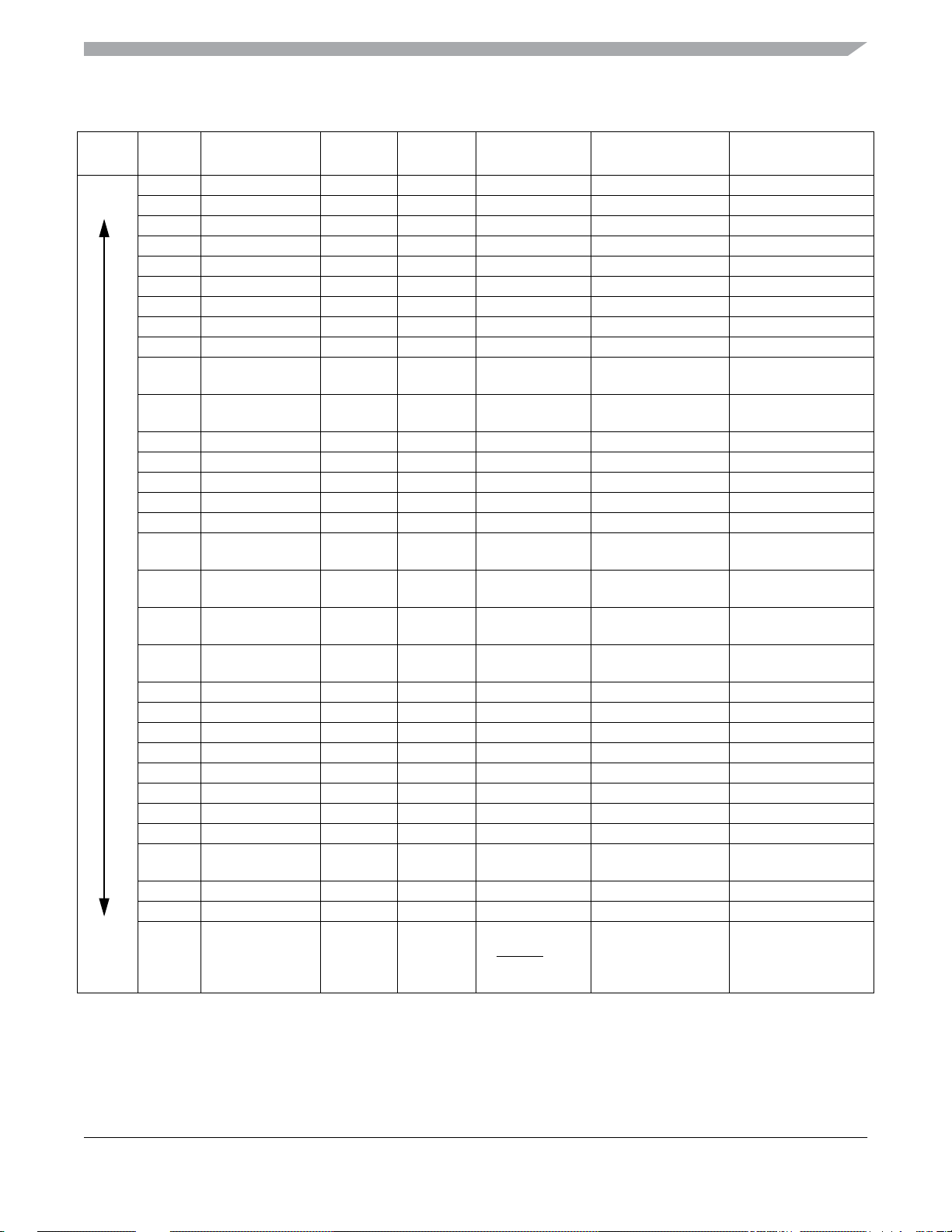
Chapter 5 Resets, Interrupts, and General System Control
Table 5-2. Vector Summary
Vector
Priority
Vector
Number
Address
(High/Low)
Vector
Name
Module Source Enable Description
31 0xFFC0/0xFFC1 Vtpm3ovf TPM3 TOF TOIE TPM3 overflow
Lowest
30 0xFFC2/0xFFC3 Vtpm3ch5 TPM3 CH5F CH5IE TPM3 channel 5
29 0xFFC4/0xFFC5 Vtpm3ch4 TPM3 CH4F CH4IE TPM3 channel 4
28 0xFFC6/0xFFC7 Vtpm3ch3 TPM3 CH3F CH3IE TPM3 channel 3
27 0xFFC8/0xFFC9 Vtpm3ch2 TPM3 CH2F CH2IE TPM3 channel 2
26 0xFFCA/0xFFCB Vtpm3ch1 TPM3 CH1F CH1IE TPM3 channel 1
25 0xFFCC/0xFFCD Vtpm3ch0 TPM3 CH0F CH0IE TPM3 channel 0
24 0xFFCE/0xFFCF Vrtc RTC RTIF RTIE Real-time interrupt
23 0xFFD0/0xFFD1 Vsci2tx SCI2 TDRE, TC TIE, TCIE SCI2 transmit
22 0xFFD2/0xFFD3 Vsci2rx SCI2 IDLE, LBKDIF,
RDRF, RXEDGIF
21 0xFFD4/0xFFD5 Vsci2err SCI2 OR, NF
FE, PF
20 0xFFD6/0xFFD7 Vacmpx ACMPx
1
ACF ACIE Analog comparator x
ILIE, LBKDIE, RIE,
RXEDGIE
ORIE, NFIE,
FEIE, PFIE
SCI2 receive
SCI2 error
19 0xFFD8/0xFFD9 Vadc ADC COCO AIEN ADC
18 0xFFDA/0xFFDB Vkeyboard KBIx
17 0xFFDC/0xFFDD Viicx IICx
2
3
KBF KBIE Keyboard x pins
IICIS IICIE IICx control
16 0xFFDE/0xFFDF Vsci1tx SCI1 TDRE, TC TIE, TCIE SCI1 transmit
15 0xFFE0/0xFFE1 Vsci1rx SCI1 IDLE, LBKDIF,
RDRF, RXEDGIF
14 0xFFE2/0xFFE3 Vsci1err SCI1 OR, NF,
FE, PF
13 0xFFE4/0xFFE5 Vspi1 SPI1 SPIF, MODF,
ILIE, LBKDIE, RIE,
SCI1 receive
RXEDGIE
ORIE, NFIE,
SCI1 error
FEIE, PFIE
SPIE, SPIE, SPTIE SPI1
SPTEF
12 0xFFE6/0xFFE7 Vspi2 SPI2 SPIF, MODF,
SPIE, SPIE, SPTIE SPI2
SPTEF
11 0xFFE8/0xFFE9 Vtpm2ovf TPM2 TOF TOIE TPM2 overflow
10 0xFFEA/0xFFEB Vtpm2ch2 TPM2 CH2F CH2IE TPM2 channel 2
9 0xFFEC/0xFFED Vtpm2ch1 TPM2 CH1F CH1IE TPM2 channel 1
8 0xFFEE/0xFFEF Vtpm2ch0 TPM2 CH0F CH0IE TPM2 channel 0
7 0xFFF0/0xFFF1 Vtpm1ovf TPM1 TOF TOIE TPM1 overflow
6 0xFFF2/0xFFF3 Vtpm1ch2 TPM1 CH2F CH2IE TPM1 channel 2
5 0xFFF4/0xFFF5 Vtpm1ch1 TPM1 CH1F CH1IE TPM1 channel 1
4 0xFFF6/0xFFF7 Vtpm1ch0 TPM1 CH0F CH0IE TPM1 channel 0
3 0xFFF8/0xFFF9 Vlvd System
control
LVDF, LVWF LVDIE, LVWIE Low-voltage detect,
Low-voltage warning
2 0xFFFA/0xFFFB Virq IRQ IRQF IRQIE IRQ pin
1 0xFFFC/0xFFFD Vswi Core SWI Instruction — Software interrupt
Highest
1
ACMP1 and ACMP2 share this vector, if both modules are enabled user should poll each flag to determine pending interrupt.
2
KBI1 and KBI2 share this vector, if both modules are enabled user should poll each flag to determine pending interrupt.
3
IIC1 and IIC2 share this vector, if both modules are enabled user should poll each flag to determine pending interrupt.
control
0 0xFFFE/0xFFFF Vreset System
COP,
LVD,
RESET pin,
Illegal opcode,
COPE
LVDRE
—
—
Watchdog timer
Low-voltage detect
External pin
Illegal opcode
MC9S08QE128 MCU Series Reference Manual, Rev. 2
Freescale Semiconductor 95
Page 96

Chapter 5 Resets, Interrupts, and General System Control
5.6 Low-Voltage Detect (LVD) System
The MC9S08QE128 Series includes a system to protect against low voltage conditions to protect memory
contents and control MCU system states during supply voltage variations. The system is comprised of a
power-onreset (POR) circuit and a LVD circuit with a user selectable trip voltage, either high (V
low (V
). The LVD circuit is enabled when LVDE in SPMSC1 is set and the trip voltage is selected
LVDL
by LVDV in SPMSC3. The LVD is disabled upon entering either of the stop modes unless LVDSE is set
in SPMSC1. If LVDSE and LVDE are both set, then the MCU will enter stop3 instead of stop2, and the
current consumption in stop3 with the LVD enabled will be greater.
5.6.1 Power-On Reset Operation
When power is initially applied to the MCU, or when the supply voltage drops below the power-on reset
rearm voltage level, V
, the POR circuit will cause a reset condition. As the supply voltage rises, the
POR
LVD circuit will hold the MCU in reset until the supply has risen above the low voltage detection low
threshold, V
. Both the POR bit and the LVD bit in SRS are set following a POR.
LVDL
5.6.2 Low-Voltage Detection (LVD) Reset Operation
The LVD can be configured to generate a reset upon detection of a low voltage condition by setting
LVDRE to 1. The low voltage detection threshold is determined by the LVDV bit. After an LVD reset has
occurred, the LVD system will hold the MCU in reset until the supply voltage has risen above the low
voltage detection threshold. The LVD bit in the SRS register is set following either an LVD reset or POR.
LVDH
)or
5.6.3 Low-Voltage Detection (LVD) Interrupt Operation
When a low voltage condition is detected and the LVD circuit is configured using SPMSC1 for interrupt
operation (LVDE set, LVDIE set, and LVDRE clear), then LVDF in SPMSC1 will be set and an LVD
interrupt request will occur. The LVDF bit is cleared by writing a 1 to the LVDACK bit in SPMSC1.
5.6.4 Low-Voltage Warning (LVW) Interrupt Operation
The LVD system has a low voltage warning flag (LVWF) to indicate to the user that the supply voltage is
approaching, but is above, the LVD voltage. The LVWalso has an interrupt associated with it, enabled by
setting the LVWIE bit in the SPMSC3 register. If enabled, an LVW interrupt request will occur when the
LVWF is set. LVWF is cleared by writing a 1 to the LVWACK bit in SPMSC3. There are two user
selectable trip voltages for the LVW,one high (V
) and one low (V
LVWH
). The trip voltage is selected
LVWL
by LVWV in SPMSC3.
5.7 Peripheral Clock Gating
The MC9S08QE128 Series includes a clock gating system to manage the bus clock sources to the
individual peripherals. Using this system, the user can enable or disable the bus clock to each of the
peripherals at the clock source, eliminating unnecessary clocks to peripherals which are not in use and
thereby reducing the overall run and wait mode currents.
MC9S08QE128 MCU Series Reference Manual, Rev. 2
96 Freescale Semiconductor
Page 97

Chapter 5 Resets, Interrupts, and General System Control
Out of reset, all peripheral clocks will be enabled. For lowest possible run or wait currents, user software
should disable the clock source to any peripheral not in use. The actual clock will be enabled or disabled
immediately following the write to the Clock Gating Control registers (SCGC1 and SCGC2). Any
peripheral with a gated clock can not be used unless its clock is enabled. Writing to the registers of a
peripheral with a disabled clock has no effect.
NOTE
User software should disable the peripheral before disabling the clocks to
the peripheral. When clocks are re-enabled to a peripheral, the peripheral
registers need to be re-initialized by user software.
In stop modes, the bus clock is disabled for all gated peripherals, regardless of the settings in SCGC1 and
SCGC2.
MC9S08QE128 MCU Series Reference Manual, Rev. 2
Freescale Semiconductor 97
Page 98
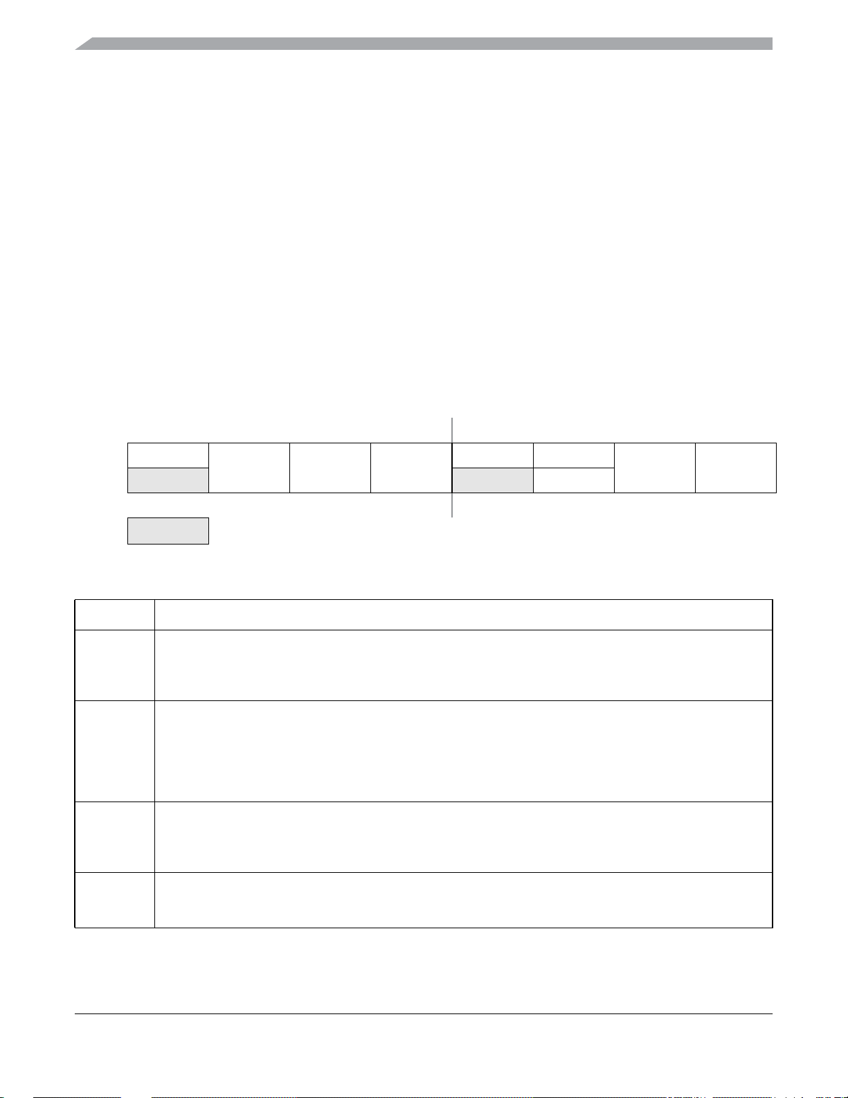
Chapter 5 Resets, Interrupts, and General System Control
IRQ was Power On Reset ENABLED on old MC68HC908GP32
5.8 Reset, Interrupt, and System Control Registers and Control Bits
One 8-bit register in the direct page register space and eight 8-bit registers in the high-page register space
are related to reset and interrupt systems.
Refer to Table 4-2 and Table 4-3 in Chapter 4, “Memory,” of this data sheet for the absolute address
assignments for all registers. This section refers to registers and control bits only by their names. A
Freescale-provided equate or header file is used to translate these names into the appropriate absolute
addresses.
Some control bits in the SOPT1 and SPMSC2 registers are related to modes of operation. Although brief
descriptions of these bits are provided here, the related functions are discussed in greater detail in
Chapter 3, “Modes of Operation.”
5.8.1 Interrupt Pin Request Status and Control Register (IRQSC)
This direct page register includes status and control bits which are used to configure the IRQ function,
report status, and acknowledge IRQ events.
76543210
R0
IRQPDD IRQEDG IRQPE
W IRQACK
IRQF 0
IRQIE IRQMOD
Reset 00000000
= Unimplemented or Reserved
Figure 5-2. Interrupt Request Status and Control Register (IRQSC)
Table 5-3. IRQSC Register Field Descriptions
Field Description
6
IRQPDD
5
IRQEDG
4
IRQPE
3
IRQF
Interrupt Request (IRQ) Pull Device Disable— This read/write control bit is used to disable the internal
pull-up/pull-down device when the IRQ pin is enabled (IRQPE = 1) allowing for an external device to be used.
0 IRQ pull device enabled if IRQPE = 1.
1 IRQ pull device disabled if IRQPE = 1.
Interrupt Request (IRQ) Edge Select — This read/write control bit is used to select the polarity of edges or
levels on the IRQ pin that cause IRQF to be set. The IRQMOD control bit determines whether the IRQ pin is
sensitive to both edges and levels or only edges. When IRQEDG = 1 and the internal pull device is enabled, the
pull-up device is reconfigured as an optional pull-down device.
0 IRQ is falling edge or falling edge/low-level sensitive.
1 IRQ is rising edge or rising edge/high-level sensitive.
IRQ Pin Enable — This read/write control bit enables the IRQ pin function. When this bit is set the IRQ pin can
be used as an interrupt request.
0 IRQ pin function is disabled.
1 IRQ pin function is enabled.
IRQ Flag — This read-only status bit indicates when an interrupt request event has occurred.
0 No IRQ request.
1 IRQ event detected.
MC9S08QE128 MCU Series Reference Manual, Rev. 2
98 Freescale Semiconductor
Page 99
Chapter 5 Resets, Interrupts, and General System Control
Table 5-3. IRQSC Register Field Descriptions
Field Description
2
IRQACK
1
IRQIE
0
IRQMOD
IRQ Acknowledge — This write-only bit is used to acknowledge interrupt request events (write 1 to clear IRQF).
Writing 0 has no meaning oreffect.Readsalwaysreturn0. If edge-and-leveldetection is selected (IRQMOD = 1),
IRQF cannot be cleared while the IRQ pin remains at its asserted level.
IRQ Interrupt Enable — This read/write control bit determines whether IRQ events generate an interrupt
request.
0 Interrupt request when IRQF set is disabled (use polling).
1 Interrupt requested whenever IRQF = 1.
IRQ Detection Mode — This read/write control bit selects either edge-only detection or edge-and-level
detection. The IRQEDG control bit determines the polarity of edges and levels that are detected as interrupt
request events. SeeSection 5.5.2.2, “Edge and Level Sensitivity” for more details.
0 IRQ event on falling edges or rising edges only.
1 IRQ event on falling edges and low levels or on rising edges and high levels.
5.8.2 System Reset Status Register (SRS)
This high page register includes read-only status flags to indicate the source of the most recent reset. When
a debug host forces reset by writing 1 to BDFR in the SBDFR register, none of the status bits in SRS will
be set. Writing any value to this register address clears the COP watchdog timer without affecting the
contents of this register. The reset state of these bits depends on what caused the MCU to reset.
76543210
R POR PIN COP ILOP 0 0 LVD 0
W Writing any value to SRS address clears COP watchdog timer.
POR: 10000010
LVD: u
Any
other
reset:
1
u = unaffected
2
Any of these reset sources that are active at the time of reset entry will cause the corresponding bit(s) to be set; bits
corresponding to sources that are not active at the time of reset entry will be cleared.
1
0 Note
0000010
2
Note
2
Note
2
0000
Figure 5-3. System Reset Status (SRS)
MC9S08QE128 MCU Series Reference Manual, Rev. 2
Freescale Semiconductor 99
Page 100
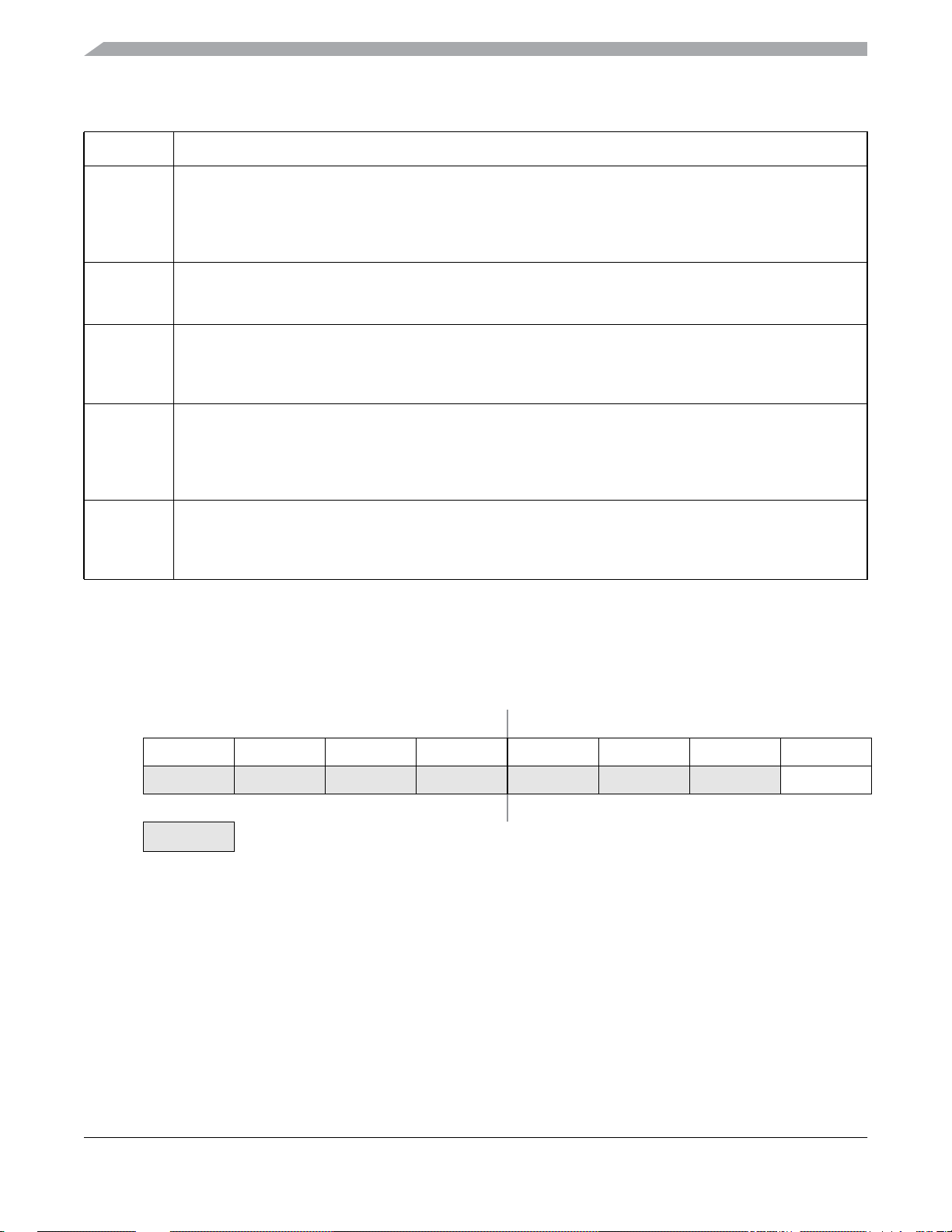
Chapter 5 Resets, Interrupts, and General System Control
Table 5-4. SRS Register Field Descriptions
Field Description
7
POR
6
PIN
5
COP
4
ILOP
1
LVD
Power-On Reset —Reset was caused bythe power-on detection logic. Because the internalsupply voltage was
ramping up at the time, the low-voltage reset (LVD) status bit is also set to indicate that the reset occurred while
the internal supply was below the LVD threshold.
0 Reset not caused by POR.
1 POR caused reset.
External Reset Pin — Reset was caused by an active-low level on the external reset pin.
0 Reset not caused by external reset pin.
1 Reset came from external reset pin.
Computer Operating Properly (COP) Watchdog — Reset was caused by the COP watchdog timer timing out.
This reset source can be blocked by COPE = 0.
0 Reset not caused by COP timeout.
1 Reset caused by COP timeout.
Illegal Opcode — Reset was caused by an attempt to execute an unimplemented or illegal opcode. The STOP
instruction is considered illegal if stop is disabled by STOPE = 0 in the SOPT register. The BGND instruction is
considered illegal if active background mode is disabled by ENBDM = 0 in the BDCSC register.
0 Reset not caused by an illegal opcode.
1 Reset caused by an illegal opcode.
Low VoltageDetect — If the LVDREbit is set and the supply drops below the LVD trip voltage, an LVD reset will
occur. This bit is also set by POR.
0 Reset not caused by LVD trip or POR.
1 Reset caused by LVD trip or POR.
5.8.3 System Background Debug Force Reset Register (SBDFR)
This high page register contains a single write-only control bit. A serial background command such as
WRITE_BYTE must be used to write to SBDFR. Attempts to write this register from a user program are
ignored. Reads always return 0x00.
76543210
R00000000
W BDFR
Reset: 00000000
= Unimplemented or Reserved
1
BDFR is writable only through serial background debug commands, not from user programs.
Figure 5-4. System Background Debug Force Reset Register (SBDFR)
1
MC9S08QE128 MCU Series Reference Manual, Rev. 2
100 Freescale Semiconductor
 Loading...