

www.ti.com
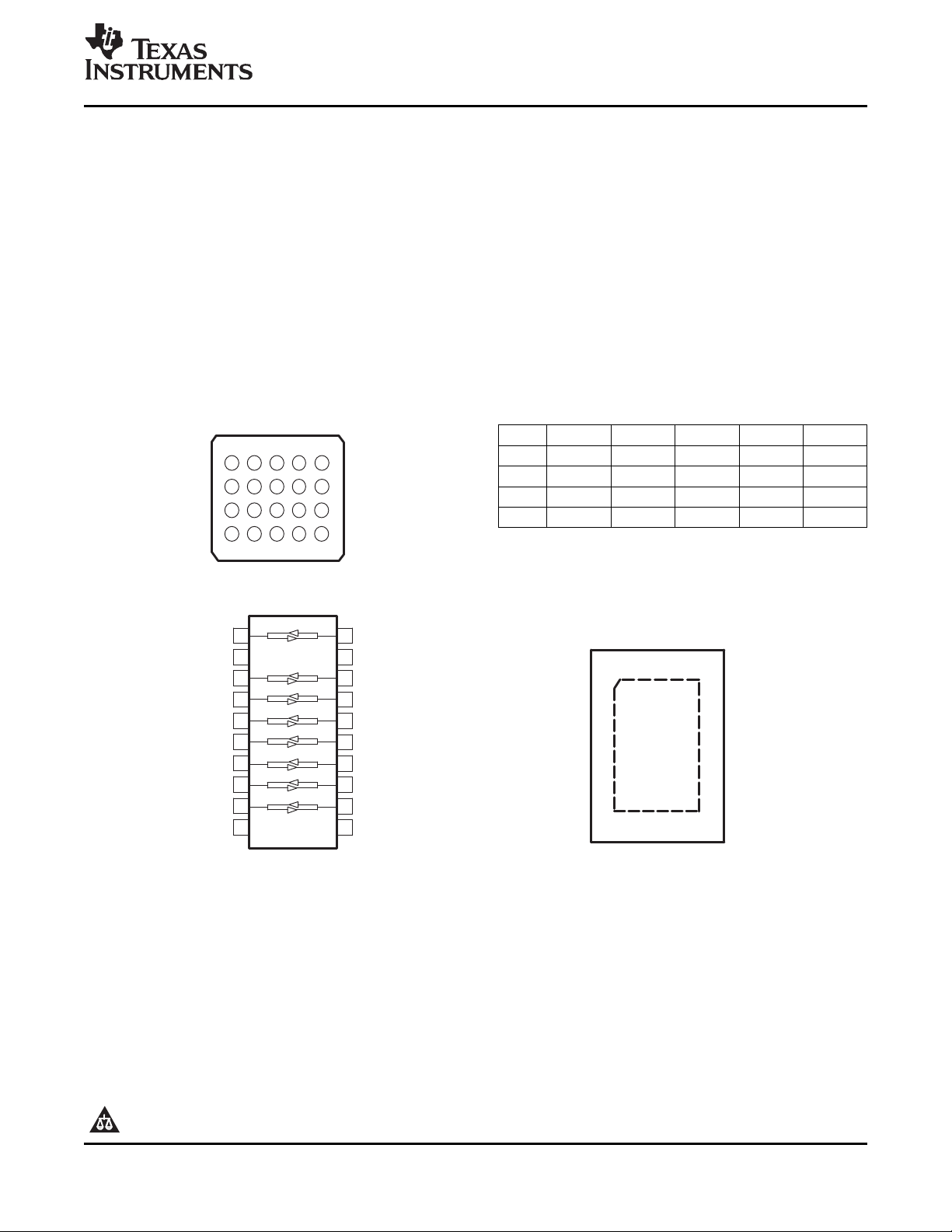
GXY OR ZXY PACKAGE
(BOTTOM VIEW)
A
B
C
D
21 3 4 5
20
19
16
15
14
13
1
2
5
6
7
8
PW PACKAGE
(TOP VIEW)
18
17
12
11
3
4
9
10
RGY PACKAGE
(TOP VIEW)
1 20
10 11
2
3
4
5
6
7
8
9
19
18
17
16
15
14
13
12
V
CCB
B2
B3
B4
B5
B6
B7
B8
V
CCA
A2
A3
A4
A5
A6
A7
A8
GND
B1
A1
OE
V
CCB
B2
B3
B4
B5
B6
B7
B8
GND
V
CCA
A1
A2
A3
A4
A5
A6
A7
A8
OE
B1
8-BIT BIDIRECTIONAL VOLTAGE-LEVEL TRANSLATOR
WITH AUTO-DIRECTION SENSING AND ± 15-kV ESD PROTECTION
SCES643A – NOVEMBER 2006 – REVISED JANUARY 2007
FEATURES
• 1.2 V to 3.6 V on A Port and 1.65 to 5.5 V on • ESD Protection Exceeds JESD 22
B Port (V
• V
Isolation Feature – If Either V
CC
GND, All Outputs Are in the High-Impedance
State
• OE Input Circuit Referenced to V
• Low Power Consumption, 4- µ A Max I
• I
Supports Partial-Power-Down Mode
off
Operation
• Latch-Up Performance Exceeds 100 mA Per
JESD 78, Class II
≤ V
CCA
)
CCB
Input Is at
CC
– A Port
– 2000-V Human-Body Model (A114-B)
– 200-V Machine Model (A115-A)
– 1000-V Charged-Device Model (C101)
CCA
CC
– B Port
– ± 15-kV Human-Body Model (A114-B)
– 200-V Machine Model (A115-A)
– 1000-V Charged-Device Model (C101)
TERMINAL ASSIGNMENTS
(20-Ball GXY/ZXY Package)
1 2 3 4 5
D V
C B1 B3 B5 B7 GND
B A1 A3 A5 A7 OE
A V
CCB
CCA
B2 B4 B6 B8
A2 A4 A6 A8
TXB0108
DESCRIPTION/ORDERING INFORMATION
This 8-bit noninverting translator uses two separate configurable power-supply rails. The A port is designed to
track V
accepts any supply voltage from 1.65 V to 5.5 V. This allows for universal low-voltage bidirectional translation
between any of the 1.2-V, 1.5-V, 1.8-V, 2.5-V, 3.3-V, and 5-V voltage nodes. V
When the output-enable (OE) input is low, all outputs are placed in the high-impedance state.
The TXB0101 is desinged so that the OE input circuit is supplied by V
PRODUCTION DATA information is current as of publication date.
Products conform to specifications per the terms of the Texas
Instruments standard warranty. Production processing does not
necessarily include testing of all parameters.
. V
CCA
Please be aware that an important notice concerning availability, standard warranty, and use in critical applications of Texas
Instruments semiconductor products and disclaimers thereto appears at the end of this data sheet.
accepts any supply voltage from 1.2 V to 3.6 V. The B port is designed to track V
CCA
CCA
.
CCA
Copyright © 2006–2007, Texas Instruments Incorporated
should not exceed V
. V
CCB
CCB
.
CCB
www.ti.com
TXB0108
8-BIT BIDIRECTIONAL VOLTAGE-LEVEL TRANSLATOR
WITH AUTO-DIRECTION SENSING AND ± 15-kV ESD PROTECTION
SCES643A – NOVEMBER 2006 – REVISED JANUARY 2007
DESCRIPTION/ORDERING INFORMATION (CONTINUED)
This device is fully specified for partial-power-down applications using I
preventing damaging current backflow through the device when it is powered down.
To ensure the high-impedance state during power up or power down, OE should be tied to GND through a
pulldown resistor; the minimum value of the resistor is determined by the current-sourcing capability of the
driver.
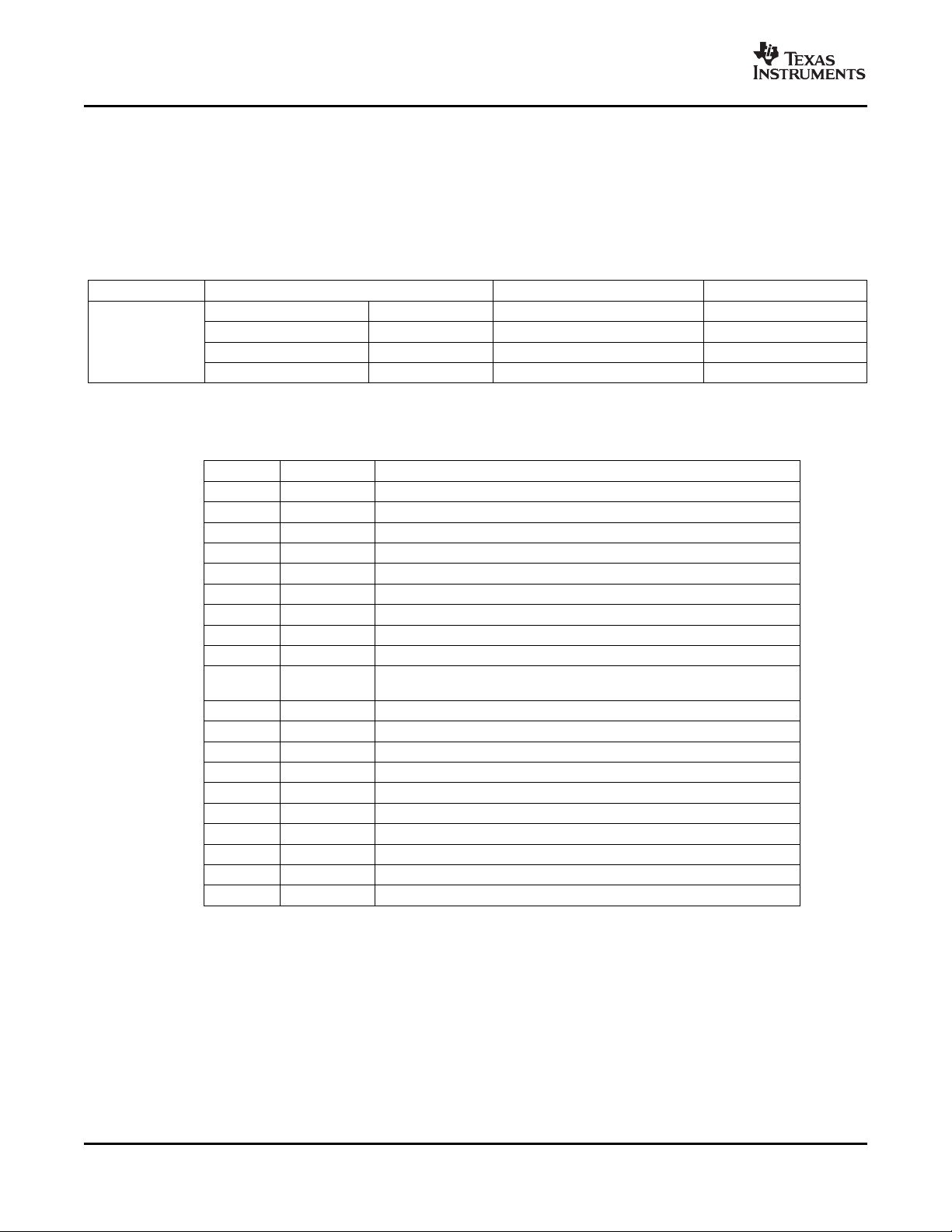
ORDERING INFORMATION
T
A
PACKAGE
QFN – RGY Reel of 1000 TXB0108RGYR YE08
–40 ° C to 85 ° C
TSSOP – PW Reel of 2000 TXB0108PWR YE08
VFBGA – GXY Reel of 2500 TXB0108GXYR YE08
VFBGA – ZXY (Pb-free) Reel of 2500 TXB0108ZXYR YE08
(1) Package drawings, standard packing quantities, thermal data, symbolization, and PCB design guidelines are available at
www.ti.com/sc/package.
(1)
ORDERABLE PART NUMBER TOP-SIDE MARKING
PIN DESCRIPTION
NO. NAME FUNCTION
1 A1 Input/output 1. Referenced to V
2 V
CCA
3 A2 Input/output 2. Referenced to V
4 A3 Input/output 3. Referenced to V
5 A4 Input/output 4. Referenced to V
6 A5 Input/output 5. Referenced to V
7 A6 Input/output 6. Referenced to V
8 A7 Input/output 7. Referenced to V
9 A8 Input/output 8. Referenced to V
10 OE
11 GND Ground
12 B8 Input/output 8. Referenced to V
13 B7 Input/output 7. Referenced to V
14 B6 Input/output 6. Referenced to V
15 B5 Input/output 5. Referenced to V
16 B4 Input/output 4. Referenced to V
17 B3 Input/output 3. Referenced to V
18 B2 Input/output 2. Referenced to V
19 V
CCB
20 B1 Input/output 1. Referenced to V
A-port supply voltage. 1.1 V ≤ V
Output enable. Pull OE low to place all outputs in 3-state mode.
Referenced to V
.
CCA
B-port supply voltage. 1.65 V ≤ V
CCA
CCA
CCA
CCA
CCA
CCA
CCA
CCA
CCB
CCB
CCB
CCB
CCB
CCB
CCB
CCB
CCA
CCB
off
.
≤ 3.6 V, V
.
.
.
.
.
.
.
.
.
.
.
.
.
.
≤ 5.5 V.
.
. The I
circuitry disables the outputs,
off
≤ V
CCA
CCB
.
2
Submit Documentation Feedback

www.ti.com
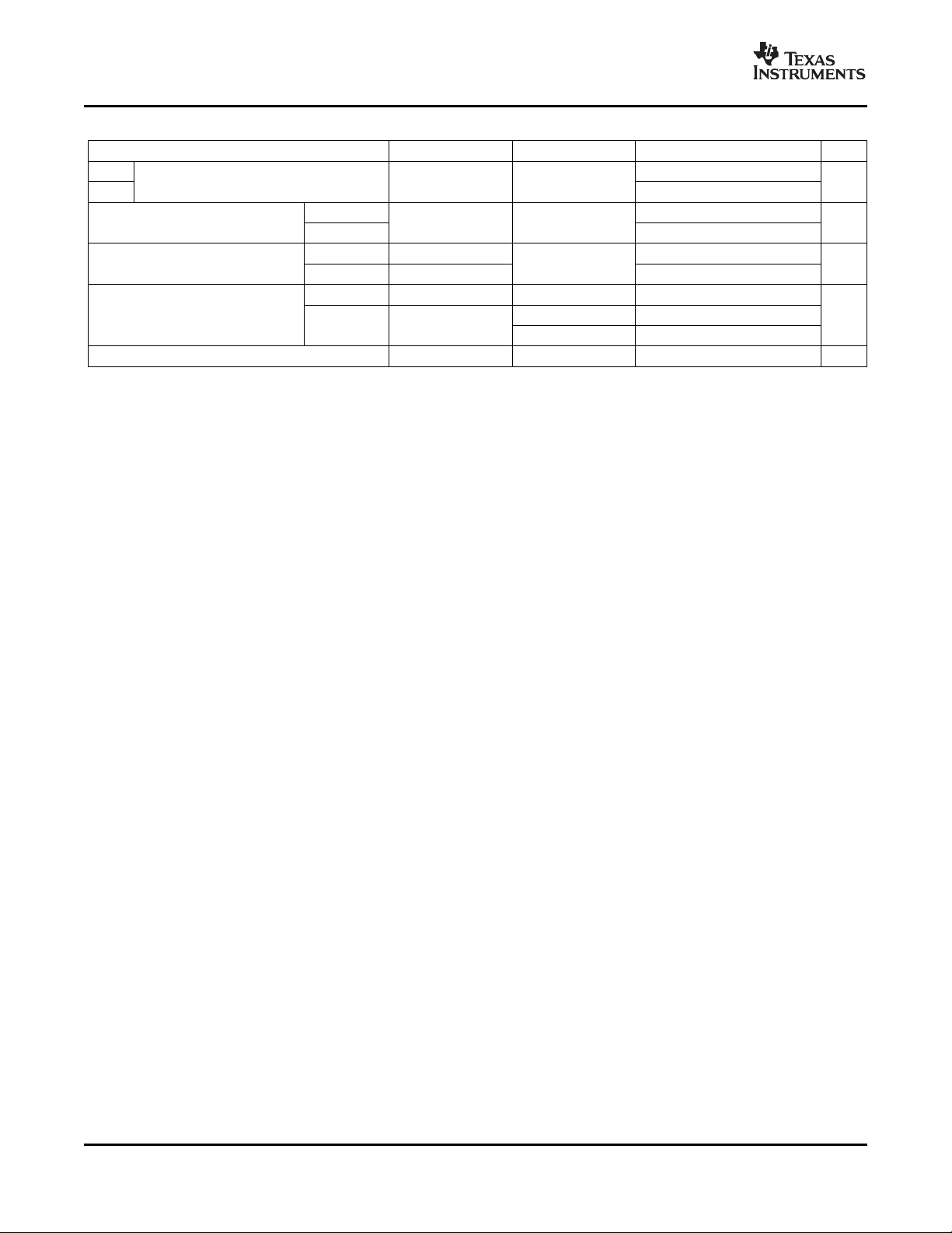
OE
A1
A2
A3
A4
A5
A6
A7
A8
B1
B2
B3
B4
B5
B6
B7
B8
3.3-V
System
1.8 -V
System
Data
Data
Controller
1.8 V
3.3 V
TXB0108
V
CCA
V
CCB
8-BIT BIDIRECTIONAL VOLTAGE-LEVEL TRANSLATOR
WITH AUTO-DIRECTION SENSING AND ± 15-kV ESD PROTECTION
SCES643A – NOVEMBER 2006 – REVISED JANUARY 2007
TYPICAL OPERATING CIRCUIT
TXB0108
Absolute Maximum Ratings
(1)
over operating free-air temperature range (unless otherwise noted)
MIN MAX UNIT
V
Supply voltage range –0.5 4.6 V
CCA
V
Supply voltage range –0.5 6.5 V
CCB
V
Input voltage range
I
V
Voltage range applied to any output in the high-impedance or power-off state
O
V
Voltage range applied to any output in the high or low state
O
I
Input clamp current VI< 0 –50 mA
IK
I
Output clamp current VO< 0 –50 mA
OK
I
Continuous output current ± 50 mA
O
Continuous current through V
θ
Package thermal impedance PW package
JA
T
stg
Storage temperature range –65 150 ° C
(1) Stresses beyond those listed under "absolute maximum ratings" may cause permanent damage to the device. These are stress ratings
only, and functional operation of the device at these or any other conditions beyond those indicated under "recommended operating
conditions" is not implied. Exposure to absolute-maximum-rated conditions for extended periods may affect device reliability.
(2) The input and output negative-voltage ratings may be exceeded if the input and output current ratings are observed.
(3) The value of V
(4) The package thermal impedance is calculated in accordance with JESD 51-7.
(5) The package thermal impedance is calculated in accordance with JESD 51-5.
CCA
and V
(2)
, V
CCA
are provided in the recommended operating conditions table.
CCB
, or GND ± 100 mA
CCB
Submit Documentation Feedback
–0.5 6.5 V
(2)
(2) (3)
A inputs –0.5 V
B inputs –0.5 V
GXY/ZXY package
RGY package
(4)
(4)
(5)
–0.5 6.5 V
+ 0.5
CCA
+ 0.5
CCB
V
78
83 ° C/W
37
3
www.ti.com
TXB0108
8-BIT BIDIRECTIONAL VOLTAGE-LEVEL TRANSLATOR
WITH AUTO-DIRECTION SENSING AND ± 15-kV ESD PROTECTION
SCES643A – NOVEMBER 2006 – REVISED JANUARY 2007
Recommended Operating Conditions
V
CCA
Supply voltage V
V
CCB
V
High-level input voltage 1.2 V to 3.6 V 1.65 V to 5.5 V V
IH
V
Low-level input voltage 1.65 V to 5.5 V V
IL
Input transition
∆ t/ ∆ v 1.65 V to 3.6 V 40 ns/V
rise or fall rate
T
Operating free-air temperature –40 85 ° C
A
(1) The A and B sides of an unused data I/O pair must be held in the same state, i.e., both at V
(2) V
(3) V
must be less than or equal to V
CCA
is the supply voltage associated with the input port.
CCI
Data inputs V
OE V
Data inputs 1.2 V to 5.5 V 0 V
OE 1.2 V to 3.6 V 0 V
A-port inputs 1.2 V to 3.6 V 1.65 V to 5.5 V 40
B-port inputs 1.2 V to 3.6 V
and must not exceed 3.6 V.
CCB
(1) (2)
V
CCA
V
CCB
MIN MAX UNIT
1.2 3.6
1.65 5.5
(3)
x 0.65
CCI
x 0.65 5.5
CCA
x 0.35
CCI
CCA
4.5 V to 5.5 V 30
or both at GND.
CCI
V
CCI
(3)
x 0.35
4
Submit Documentation Feedback

www.ti.com
8-BIT BIDIRECTIONAL VOLTAGE-LEVEL TRANSLATOR
WITH AUTO-DIRECTION SENSING AND ± 15-kV ESD PROTECTION
Electrical Characteristics
over recommended operating free-air temperature range (unless otherwise noted)
PARAMETER V
V
V
V
V
I
I
I
I
I
I
I
I
C
C
(1) V
(2) V
OHA
OLA
OHB
OLB
OE 1.2 V to 3.6 V 1.65 V to 5.5 V ± 1 ± 2 µ A
I
A port 0 V 0 V to 5.5 V ± 1 ± 2
off
B port 0 V to 3.6 V 0 V ± 1 ± 2
A or B port OE = GND 1.2 V to 3.6 V 1.65 V to 5.5 V ± 1 ± 2 µ A
OZ
CCA
CCB
+ I
CCA
CCB
CCZA
CCZB
OE 1.2 V to 3.6 V 1.65 V to 5.5 V 5 5.5 pF
I
A port 5 6.5
io
B port 8 10
is the supply voltage associated with the input port.
CCI
is the supply voltage associated with the output port.
CCO
IOH= –20 µ A V
IOL= 20 µ A V
IOH= –20 µ A 1.65 V to 5.5 V V
IOL= 20 µ A 1.65 V to 5.5 V 0.4 V
VI= V
IO= 0
VI= V
IO= 0
VI= V
IO= 0
VI= V
IO= 0, 1.65 V to 5.5 V µ A
OE = GND
VI= V
IO= 0, 1.65 V to 5.5 V µ A
OE = GND
(1) (2)
TEST
CONDITIONS
CCA
V
1.2 V 1.1
1.4 V to 3.6 V V
1.2 V 0.9
1.4 V to 3.6 V 0.4
1.2 V 0.06
or GND,
CCI
1.4 V to 3.6 V 5
1.65 V to 5.5 V
3.6 V 0 V 2
0 V 5.5 V –2
1.2 V 3.4
or GND,
CCI
1.4 V to 3.6 V 5
1.65 V to 5.5 V
3.6 V 0 V –2
0 V 5.5 V 2
or GND,
CCI
or GND, 1.2 V 0.05
CCI
1.2 V 3.5
1.4 V to 3.6 V 10
1.65 V to 5.5 V µ A
1.4 V to 3.6 V 5
or GND, 1.2 V 3.3
CCI
1.4 V to 3.6 V 5
1.2 V to 3.6 V 1.65 V to 5.5 V pF
TXB0108
SCES643A – NOVEMBER 2006 – REVISED JANUARY 2007
CCB
MIN TYP MAX MIN MAX
– 0.4
CCA
– 0.4 V
CCB
TA= 25 ° C –40 ° C to 85 ° C
UNIT
µ A
µ A
µ A
Timing Requirements
TA= 25 ° C, V
t
w
Data rate 20 20 20 20 Mbps
Pulse duration Data inputs 50 50 50 50 ns
= 1.2 V
CCA
Timing Requirements
over recommended operating free-air temperature range, V
Data rate 50 50 50 50 Mbps
t
Pulse duration Data inputs 20 20 20 20 ns
w
Submit Documentation Feedback
V
CCB
= 1.8 V V
CCB
= 2.5 V V
CCB
= 3.3 V V
TYP TYP TYP TYP
= 1.5 V ± 0.1 V (unless otherwise noted)
CCA
V
= 1.8 V V
CCB
± 0.15 V ± 0.2 V ± 0.3 V ± 0.5 V
CCB
= 2.5 V V
CCB
= 3.3 V V
MIN MAX MIN MAX MIN MAX MIN MAX
= 5 V
CCB
= 5 V
CCB
UNIT
UNIT
5
www.ti.com
TXB0108
8-BIT BIDIRECTIONAL VOLTAGE-LEVEL TRANSLATOR
WITH AUTO-DIRECTION SENSING AND ± 15-kV ESD PROTECTION
SCES643A – NOVEMBER 2006 – REVISED JANUARY 2007
Timing Requirements
over recommended operating free-air temperature range, V
Data rate 52 60 60 60 Mbps
t
Pulse duration Data inputs 19 17 17 17 ns
w
Timing Requirements
over recommended operating free-air temperature range, V
Data rate 70 100 100 Mbps
t
Pulse duration Data inputs 14 10 10 ns
w
Timing Requirements
over recommended operating free-air temperature range, V
Data rate 100 100 Mbps
t
w
Pulse duration Data inputs 10 10 ns
= 1.8 V ± 0.15 V (unless otherwise noted)
CCA
V
= 1.8 V V
CCB
± 0.15 V ± 0.2 V ± 0.3 V ± 0.5 V
CCB
= 2.5 V V
CCB
= 3.3 V V
MIN MAX MIN MAX MIN MAX MIN MAX
= 2.5 V ± 0.2 V (unless otherwise noted)
CCA
V
= 2.5 V V
CCB
± 0.2 V ± 0.3 V ± 0.5 V
= 3.3 V V
CCB
MIN MAX MIN MAX MIN MAX
= 3.3 V ± 0.3 V (unless otherwise noted)
CCA
V
= 3.3 V V
CCB
± 0.3 V ± 0.5 V
CCB
MIN MAX MIN MAX
= 5 V
CCB
UNIT
= 5 V
CCB
UNIT
= 5 V
UNIT
Switching Characteristics
TA= 25 ° C, V
PARAMETER UNIT
t
pd
t
en
t
dis
trA, t
trB, t
t
SK(O)
Max data rate 20 20 20 20 Mbps
= 1.2 V
CCA
V
FROM TO
(INPUT) (OUTPUT)
= 1.8 V V
CCB
TYP TYP TYP TYP
CCB
= 2.5 V V
CCB
= 3.3 V V
CCB
A B 9.5 7.9 7.6 8.5
B A 9.2 8.8 8.4 8
OE µ s
OE ns
fA
fB
A-port rise and fall times 4.1 4.4 4.1 3.9 ns
B-port rise and fall times 5 5 5.1 5.1 ns
A 1 1 1 1
B 1 1 1 1
A 20 17 17 18
B 20 16 15 15
Channel-to-channel skew 2.4 1.7 1.9 7 ns
= 5 V
ns
6
Submit Documentation Feedback
www.ti.com
8-BIT BIDIRECTIONAL VOLTAGE-LEVEL TRANSLATOR
WITH AUTO-DIRECTION SENSING AND ± 15-kV ESD PROTECTION
SCES643A – NOVEMBER 2006 – REVISED JANUARY 2007
Switching Characteristics
over recommended operating free-air temperature range, V
PARAMETER UNIT
t
pd
t
en
t
dis
trA, t
fA
trB, t
fB
t
SK(O)
Max data rate 50 50 50 50 Mbps
FROM TO
(INPUT) (OUTPUT)
A B 1.4 12.9 1.2 10.1 1.1 10 0.8 9.9
B A 0.9 14.2 0.7 12 0.4 11.7 0.3 13.7
OE µ s
OE ns
A 1 1 1 1
B 1 1 1 1
A 6.6 33 6.4 25.3 6.1 23.1 5.9 24.6
B 6.6 35.6 5.8 25.6 5.5 22.1 5.6 20.6
A-port rise and fall times 0.8 6.5 0.8 6.3 0.8 6.3 0.8 6.3 ns
B-port rise and fall times 1 7.3 0.7 4.9 0.7 4.6 0.6 4.6 ns
Channel-to-channel skew 2.6 1.9 1.6 1.3 ns
Switching Characteristics
over recommended operating free-air temperature range, V
PARAMETER UNIT
t
pd
t
en
t
dis
trA, t
fA
trB, t
fB
t
SK(O)
Max data rate 52 60 60 60 Mbps
FROM TO
(INPUT) (OUTPUT)
A B 1.6 11 1.4 7.7 1.3 6.8 1.2 6.5
B A 1.5 12 1.2 8.4 0.8 7.6 0.5 7.1
OE µ s
OE ns
A 1 1 1 1
B 1 1 1 1
A 5.9 26.7 5.6 21.6 5.4 18.9 4.8 18.7
B 6.1 33.9 5.2 23.7 5 19.9 5 17.6
A-port rise and fall times 0.7 5.1 0.7 5 1 5 0.7 5 ns
B-port rise and fall times 1 7.3 0.7 5 0.7 3.9 0.6 3.8 ns
Channel-to-channel skew 0.8 0.7 0.6 0.6 ns
= 1.5 V ± 0.1 V (unless otherwise noted)
CCA
V
= 1.8 V V
CCB
± 0.15 V ± 0.2 V ± 0.3 V ± 0.5 V
CCB
= 2.5 V V
CCB
= 3.3 V V
MIN MAX MIN MAX MIN MAX MIN MAX
= 1.8 V ± 0.15 V (unless otherwise noted)
CCA
V
= 1.8 V V
CCB
± 0.15 V ± 0.2 V ± 0.3 V ± 0.5 V
CCB
= 2.5 V V
CCB
= 3.3 V V
MIN MAX MIN MAX MIN MAX MIN MAX
CCB
CCB
TXB0108
= 5 V
ns
= 5 V
ns
Submit Documentation Feedback
7
 Loading...