

Data Sheet
2.5V Drive Nch MOSFET
RU1L002SN
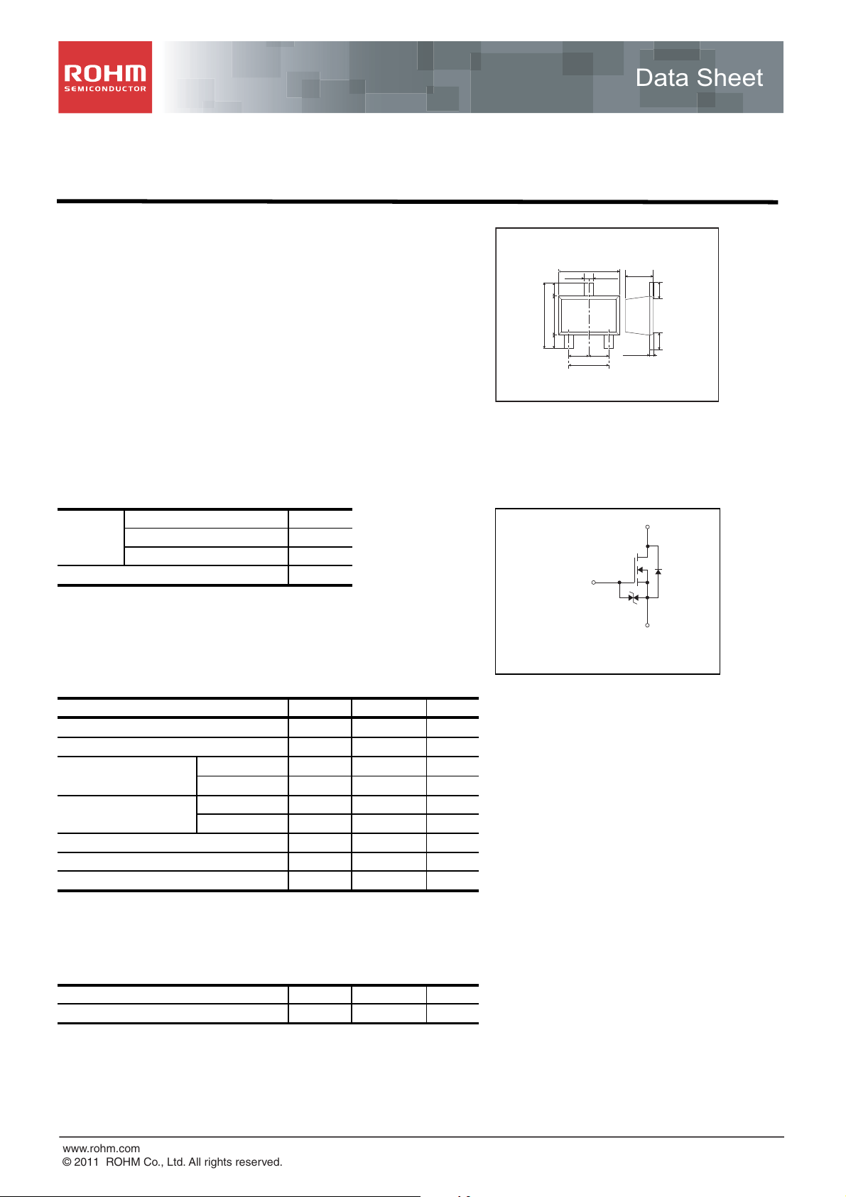
Structure Dimensions (Unit : mm)
Silicon N-channel MOSFET
UMT3F
0.32
Features
1) Low on-resistance.
0.4250.425
2.1
1.25
2) Low voltage drive (2.5V drive).
3) Small package (UMT3F).
0.65 0.65
Abbreviated symbol : RK
Application
Switching
Packaging specifications Inner circuit
Package Taping
Type
Code TCL
Basic ordering unit (pieces) 3000
RU1L002SN
(1) Gate
(2) Source
(3) Drain
2.0
(3)
(1) (2)
1.3
(1)
1 ESD PROTECTION DIODE
2 BODY DIODE
0.9
0.530.53
0.13
(3)
∗2
∗1
(2)
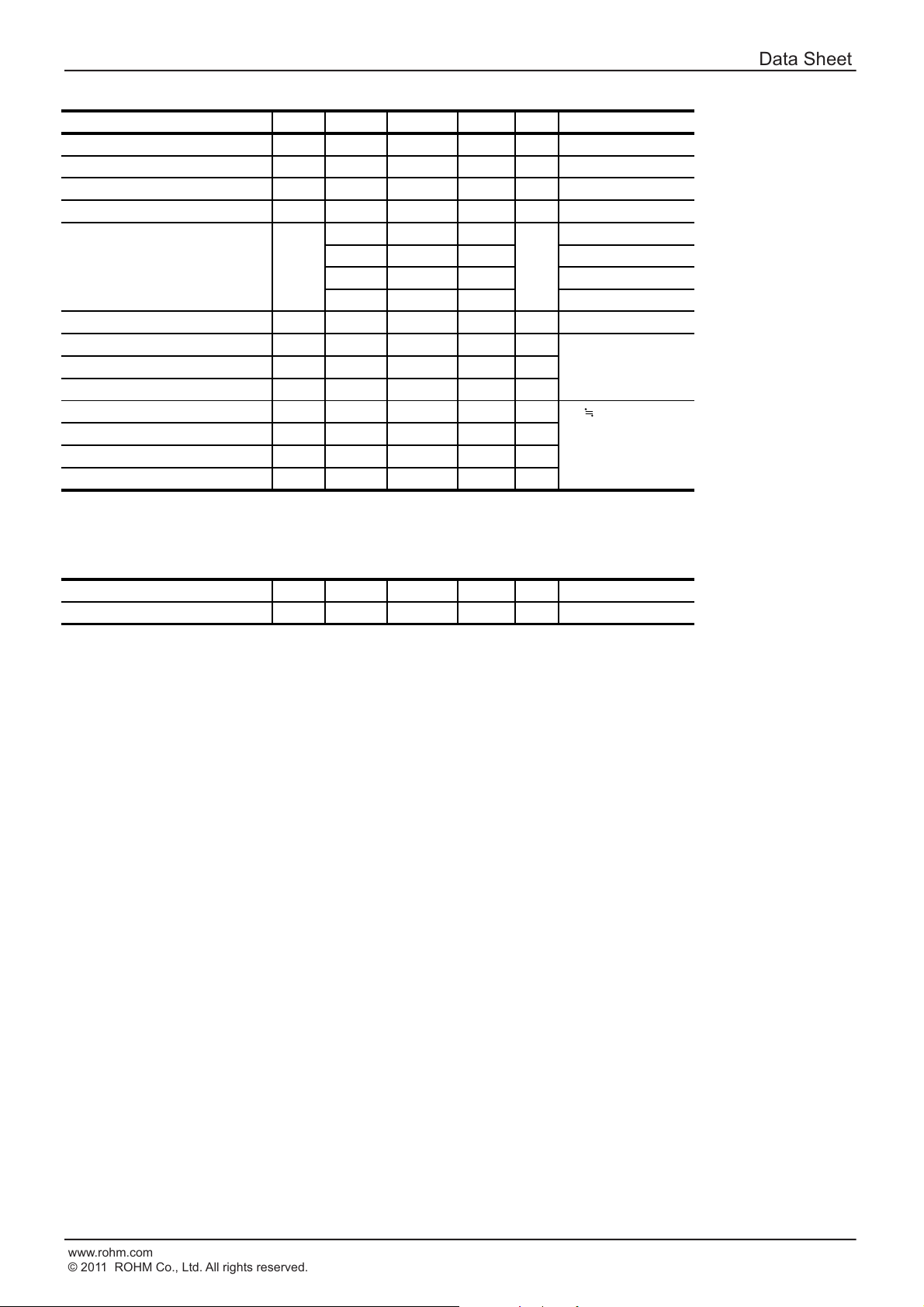
Absolute maximum ratings (Ta = 25C)
Parameter
Drain-source voltage V
Gate-source voltage V
Drain current
Source current
(Body Diode)
Continuous I
Pulsed
Continuous I
Pulsed
Power dissipation P
Symbol Limits Unit
60 V
20 V
250 mA
1
A
125 mA
1
A
200 mW
I
I
DSS
GSS
D
DP
S
SP
D
*1
*1
*2
Channel temperature Tch 150 C
Range of storage temperature Tstg 55 to 150 C
*1 Pw10s, Duty cycle1%
*2 Each terminal mounted on a recommended land
Thermal resistance
Parameter
Channel to Ambient Rth (ch-a) 625 C / W
* Each terminal mounted on a recommended land
Symbol Limits Unit
*
www.rohm.com
© 2011 ROHM Co., Ltd. All rights reserved.
1/6
2011.08 - Rev.A
www.rohm.com
© 2011 ROHM Co., Ltd. All rights reserved.
Data Sheet
RU1L002SN
Electrical characteristics (Ta = 25C)
Parameter
Gate-source leakage I
Drain-source breakdown voltage V
Zero gate voltage drain current I
Gate threshold voltage V
Symbol Min. Typ. Max. Unit
GSS
(BR)DSS
DSS
GS (th)
--10 AVGS=20V, VDS=0V
60 - - V ID=1mA, VGS=0V
--1AVDS=60V, VGS=0V
1.0 - 2.3 V VDS=10V, ID=1mA
- 1.7 2.4
Static drain-source on-state
resistance
R
DS (on)
- 2.1 3.0
***
- 2.3 3.2
- 3.0 12.0
iss
oss
rss
d(on)
d(off)
*
- 15 - pF VDS=25V
- 4.5 - pF VGS=0V
- 2.0 - pF f=1MHz
- 3.5 - ns VDD 30V, ID=100mA
*
r
f
-5-nsV
*
-18-ns
*
-28-ns
*
Forward transfer admittance l Yfs l 0.25 - - S VDS=10V, ID=250mA
Input capacitance C
Output capacitance C
Reverse transfer capacitance C
Turn-on delay time t
Rise time t
Turn-off delay time t
Fall time t
*Pulsed
Conditions
I
=250mA, VGS=10V
D
I
=250mA, VGS=4.5V
D
I
=250mA, VGS=4.0V
D
I
=10mA, VGS=2.5V
D
=10V
GS
Body diode characteristics (Source-Drain)
Parameter Conditions
Forward Voltage V
*Pulsed
Symbol Min. Typ. Max. Unit
*
SD
- - 1.2 V Is=250mA, VGS=0V
2/6
2011.08 - Rev.A
www.rohm.com
© 2011 ROHM Co., Ltd. All rights reserved.
Data Sheet
RU1L002SN
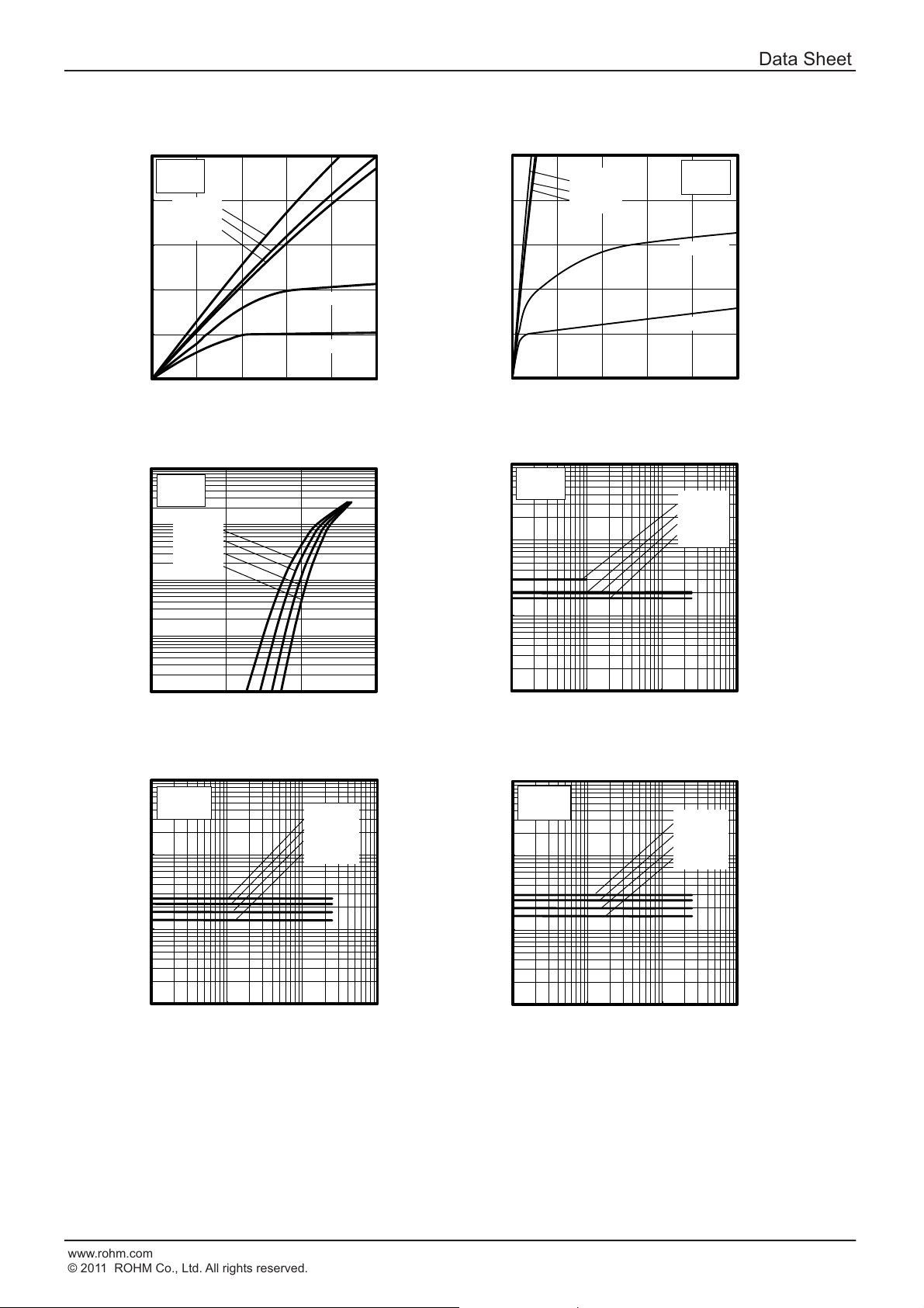
Electrical characteristic curves (Ta=25C)
0
0.1
0.2
0.3
0.4
0.5
0 0.2 0.4 0.6 0.8 1
VGS= 2.5V
VGS= 2.8V
V
GS
= 10V
VGS= 4.5V
VGS= 4.0V
Ta= 25°C
Pulsed
Fig.1 Typical Output Characteristics(Ⅰ)
DRAIN CURRENT : I
D
[A]
DRAIN-SOURCE VOLTAGE : VDS[V]
0
0.1
0.2
0.3
0.4
0.5
0 2 4 6 8 10
VGS= 2.5V
VGS= 2.8V
V
GS
= 10V
V
GS
= 4.5V
V
GS
= 4.0V
Ta= 25°C
Pulsed
Fig.2 Typical Output Characteristics(Ⅱ)
DRAIN-SOURCE VOLTAGE : VDS[V]
DRAIN CURRENT : I
D
[A]
0.0001
0.001
0.01
0.1
1
0 1 2 3
Ta=125°C
Ta=75°
C
Ta=25°
C
Ta=
-25
°C
VDS= 10V
Pulsed
Fig.3 Typical Transfer Characteristics
DRAIN CURRENT : I
D
[A]
GATE-SOURCE VOLTAGE : VGS[V]
0.1
1
10
100
0.001 0.01 0.1 1
V
GS
= 2.5V
V
GS
= 4.0V
V
GS
= 4.5V
V
GS
= 10V
Ta= 25°C
Pulsed
Fig.4 Static Drain-Source On-State Resistance vs. Drain Current(Ⅰ)
DRAIN-CURRENT : ID[A]
STATIC DRAIN-SOURCE ON-STATE
RESISTANCE : R
DS
(on)[W]
0.1
1
10
100
0.001 0.01 0.1 1
V
GS
= 10V
Pulsed
Ta=125°C
Ta=75°C
Ta=25°C
Ta= -25°C
Fig.5 Static Drain-Source On-State Resistance vs. Drain Current(Ⅱ)
DRAIN-CURRENT : ID[A]
STATIC DRAIN-SOURCE ON-STATE
RESISTANCE : R
DS
(on)[W]
0.1
1
10
100
0.001 0.01 0.1 1
V
GS
= 4.5V
Pulsed
Ta=125°C
Ta=75°C
Ta=25°C
Ta= -25°C
Fig.6 Static Drain-Source On-State Resistance vs. Drain Current(Ⅲ)
DRAIN-CURRENT : ID[A]
STATIC DRAIN-SOURCE ON-STATE
RESISTANCE : R
DS
(on)[W]
3/6
2011.08 - Rev.A

www.rohm.com
© 2011 ROHM Co., Ltd. All rights reserved.
Data Sheet
RU1L002SN
0.1
1
10
100
0.001 0.01 0.1 1
VGS= 4.0V
Pulsed
Ta=125°C
Ta=75°C
Ta=25°C
Ta= -25°C
Fig.7 Static Drain-Source On-State Resistance vs. Drain Current(Ⅳ)
DRAIN-CURRENT : ID[A]
STATIC DRAIN-SOURCE ON-STATE
RESISTANCE : R
DS
(on)[W]
0.1
1
10
100
0.001 0.01 0.1 1
V
GS
= 2.5V
Pulsed
Ta=125°C
Ta=75°C
Ta=25°C
Ta= -25°C
Fig.8 Static Drain-Source On-State Resistance vs. Drain Current(Ⅳ)
DRAIN-CURRENT : ID[A]
STATIC DRAIN-SOURCE ON-STATE
RESISTANCE : R
DS
(on)[W]
0.01
0.1
1
0.001 0.01 0.1 1
VDS= 10V
Pulsed
Ta=125°C
Ta=75°C
Ta=25°C
Ta= -25°C
Fig.9 Forward Transfer Admittance vs. Drain Current
FORWARD TRANSFER
ADMITTANCE : |Yfs| [S]
DRAIN-CURRENT : ID[A]
0.001
0.01
0.1
1
0 0.5 1 1.5
Ta=125°C
Ta=75°C
Ta=25°C
Ta= -25°C
VGS=0V
Pulsed
Fig.10 Reverse Drain Current vs. Sourse-Drain Voltage
REVERSE DRAIN CURRENT : Is [A]
SOURCE-DRAIN VOLTAGE : VSD [V]
0
2
4
6
8
0 2.5 5 7.5 10
ID= 0.25A
ID= 0.01A
Ta=25°C
Pulsed
Fig.11 Static Drain-Source On-State Resistance vs. Gate Source Voltage
STATIC DRAIN-SOURCE ON-STATE
RESISTANCE : R
DS
(on)[W]
GATE-SOURCE VOLTAGE : VGS[V]
1
10
100
1000
0.01 0.1 1
t
f
t
r
t
d(off)
t
d(on)
Ta=25°C
VDD= 30V
VGS=10V
RG=10W
Pulsed
Fig.12 Switching Characteristics
SWITCHING TIME : t [ns]
DRAIN-CURRENT : ID[A]
4/6
2011.08 - Rev.A

www.rohm.com
© 2011 ROHM Co., Ltd. All rights reserved.
Data Sheet
RU1L002SN
1
10
100
0.01 0.1 1 10 100
Fig.13 Typical Capacitance vs. Drain-Source Voltage
DRAIN-SOURCE VOLTAGE : VDS[V]
CAPACITANCE : C [pF]
Ta=25°C
f=1MHz
VGS=0V
Ciss
Coss
Crss
5/6
2011.08 - Rev.A

www.rohm.com
© 2011 ROHM Co., Ltd. All rights reserved.
Data Sheet
RU1L002SN
D
F
it
%
V
V
Measurement circuits
VGS
RG
ig.1-1 Switching Time Measurement Circu
D.U.T.
D
I
RL
VDD
VDS
GS
DS
t
Fig.1-2 Switching Waveforms
Pulse width
50%
10%
10% 10%
d(on)
90% 90
t
r
t
on
90%
t
d(off)
t
50%
off
t
f
Notice
This product might cause chip aging and breakdown under the large electrified environment. Please consider to design ES
protection circuit.
6/6
2011.08 - Rev.A

Notes
Notice
www.rohm.com
© 2011 ROHM Co., Ltd. All rights reserved.
Thank you for your accessing to ROHM product informations.
More detail product informations and catalogs are available, please contact us.
ROHM Customer Support System
http://www.rohm.com/contact/
R1120A
 Loading...