

C
10V Drive Nch MOSFET
R6015ANJ
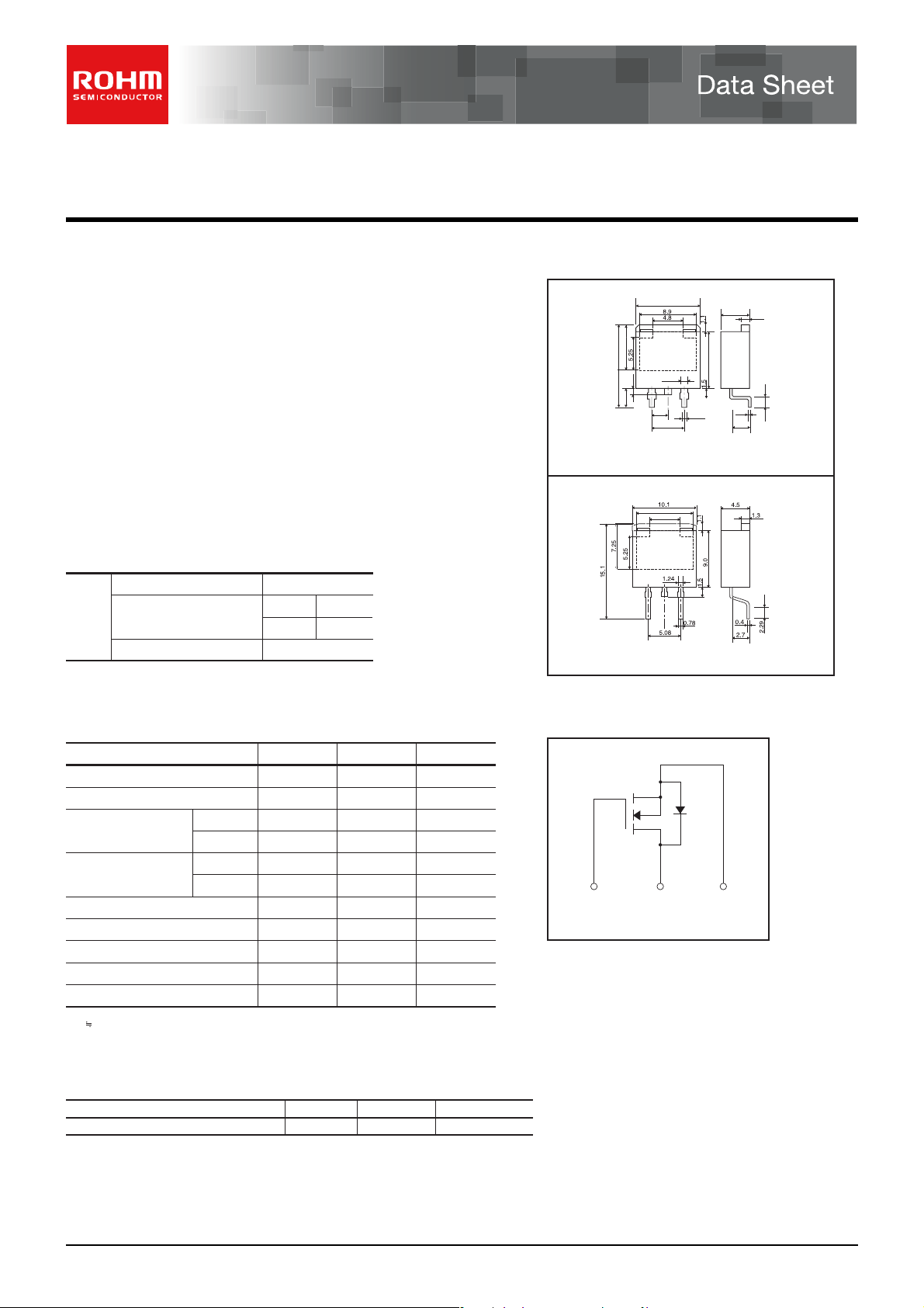
zStructure zDimensions (Unit : mm)
Silicon N-channel MOSFET
LPTS
7.25
13.1
1.0
3.0
(1) Gate
(2) Drain
(3) Source
LPTL
(1) Gate
(2) Drain
(3) Source
(1) (2) (3)
(1) Gate
(2) Drain
(3) Source
(1) (2) (3)
(1) (2) (3)
10.1
1.24
2.54
0.78
5.08
Each lead has same dimensions
8.9
4.8
Each lead has same dimensions
∗1
∗1 Body Diode
zFeatures
1) Low on-resistance.
2) Fast switching speed.
3) Gate-source voltage (V
GSS) guaranteed to be ±30V.
4) Drive circuits can be simple.
5) Parallel use is easy.
zApplications
Switching
zPackaging specifications
LPTS
LPTL
Taping
1000
TL
TLL
Package
Type
Code
Basic ordering unit (pieces)
zAbsolute maximum ratings (Ta=25°C) zInner circuit
Parameter
Drain-source voltage
Gate-source voltage
Drain current
Source current
(Body Diode)
Continuous
Pulsed
Continuous
Pulsed
Avalanche Current
Avalanche Energy
Total power dissipation (Tc=25°C)
Channel temperature
Range of storage temperature
∗1 Pw≤10µs, Duty cycle≤1%
∗2 L 500µH, V
∗3 Limited only by maximum temperature allowed
DD
=50V, RG=25Ω, Starting, Tch=25°C
Symbol
V
DSS
VGSS
I
D
IDP
IS A
I
SP A
AS
I
AS
E
PD
Tch
Tstg °C
∗3
∗1
∗3
∗1
∗2
∗2
−55 to +150
Limits
600
±30
±15
±60
15
60
7.5
15.0
100
150
Unit
V
V
A
A
A
mJ
W
°C
zThermal resistance
Parameter
hannel to case 1.25
Symbol Limits Unit
Rth(ch-c)
°C/W
4.5
1.3
9.0
0.4
1.2
2.7
www.rohm.com
c
○
2009 ROHM Co., Ltd. All rights reserved.
1/5
2009.04 - Rev.A

R6015ANJ
zElectrical characteristics (Ta=25°C)
Parameter
Gate-source leakage
Drain-source breakdown voltage
Zero gate voltage drain current
Gate threshold voltage
Static drain-source on-state resistance
Forward transfer admittance
Symbol
I
V
(BR)DSS
I
V
R
| Y
Input capacitance
Output capacitance
Reverse transfer capacitance
Turn-on delay time
C
C
t
Rise time
Turn-off delay time
t
Fall time
Total gate charge
Gate-source charge
Gate-drain charge
∗ Pulsed
Q
zBody diode characteristics (Source-drain) (Ta=25°C)
Parameter Symbol
∗ Pulsed
∗
V
SD
Min.
GSS
−
600
DSS
GS(th)
DS(on)
C
oss
rss
d(on)
t
d(off)
t
Q
Q
−
2.5
∗
−
∗
fs
|
4.5
iss
−
−
−
∗
−
∗
r
−
∗
−
∗
f
−
∗
g
−
∗
gs
−
∗
gd
−
Min. Typ. Max.
−−1.5 V IS=15A, VGS=0VForward voltage
Max. Unit Conditions
Typ.
−
−
−
−
0.23
−
1700
1120
80
50
50
150
60
50
8
20
±100
−
100
4.5
0.3
−
−
−
−
− ns
− VGS=10Vns
− RL=40Ωns
− RG=10Ωns
− V
− nC
− nC
Unit
nA V
V
µA
V
Ω
S
pF
pF
pF
nC
GS
D
=1mA, VGS=0V
I
DS
V
V
DS
D
=7.5A, VGS=10V
I
I
D
=7.5A, VDS=10V
V
DS
V
GS
f=1MHz
D
=7.5A, VDD 300V
I
DD
D
=15A
I
GS
V
L
=20Ω / RG=10Ω
R
Conditions
=±30V, VDS=0V
=600V, VGS=0V
=10V, ID=1mA
=25V
=0V
300V
=10V
Data Sheet
www.rohm.com
c
○
2009 ROHM Co., Ltd. All rights reserved.
2/5
2009.04 - Rev.A

R6015ANJ
zElectrical characteristics curves
100
10
(A)
D
1
Oper ation in thi s
area i s li mited
0.1
by R
DRAIN CURRENT : I
Tc = 25°C
Sing le Pulse
0.01
0.1 1 10 100 1000
DR AIN-SOU RCE VOLTAGE : V
PW=100us
DS(ON)
Fi g.1 M aximum Safe Oper ating Aera
PW=1ms
PW = 10ms
DC operati on
40
30
(A)
D
20
10
DRAIN CURRENT: I
0
0 1020304050
( V )
DS
DR AIN-SOU RCE VOLTAG E: VDS (V)
Fi g.2: T ypic al output char acter isti cs(Ⅰ)
8.0V
10V
6.5V
6.0V
5.0V
Ta= 25°C
Pulsed
7.0V
VGS= 4.5V
20
Ta= 25°C
Pulsed
15
(A)
D
10
5
DRAIN CURRENT: I
0
012345
10V
8.0V
7.0V
6.5V
6.0V
DRAIN-SOURCE VOLTAGE: VDS (V)
Fi g.3: T ypic al output char acter isti cs(Ⅱ)
5.0V
VGS= 4.5V
Data Sheet
5.5V
100
VDS= 10V
Pulsed
10
(A)
Ta= 125°C
D
Ta= 75°C
Ta= 25°C
1
Ta= -25°C
0.1
DRAIN CURRENT : I
0.01
01 2345 67
GATE- SOURC E VOLTAGE : VGS (V)
Fi g.4 T ypical Tr ansfer C haracter isti cs
0.6
0.5
(Ω)
0.4
DS(on)
0.3
0.2
RESIST ANCE : R
0.1
STATI C DRAIN -SOUR CE ON- STATE
0
ID=7.5A
051015
GATE-SOURCE VOLTAGE : VGS (V)
Fi g.7 Stat ic Dr ain- Source On- State
Resis tance vs. Gate Source Voltag e
ID=15A
Ta= 25°C
Pulsed
6
VDS= 10V
(V)
I
= 1mA
D
5
GS(th)
4
3
2
1
GATE T HRESHOLD VOLTAGE: V
0
-50 0 50 100 150
CH ANNEL TEM PERATUR E: Tch (°C)
Fi g.5 Gate T hreshol d Voltag e
vs. Channel Temperat ure
0.6
VGS= 10V
Pulsed
0.5
) (Ω)
0.4
DS(on
0.3
0.2
RESIST ANCE : R
0.1
STATIC DRAIN-SOURCE ON-STATE
0
-50 0 50 100 150
Fi g.8 Stat ic Dr ain- Source On- State
Res istanc e vs. C hannel Temper ature
ID= 15A
CH ANNEL TEM PERATUR E: Tch (°C)
ID= 7. 5A
10
VGS= 10V
Pulsed
(Ω)
1
DS(on)
0.1
RESISTANCE : R
STATI C DRAIN -SOUR CE ON- STATE
0.01
0.001 0.01 0.1 1 10 100
DRAIN CURRENT : ID (A)
Fi g.6 Stat ic Dr ain- Source On- State
Resis tance vs. Drain Cur rent
100
VDS= 10V
Pulsed
10
1
|Yfs| (S)
0.1
0.01
FOR WARD TRANSF ER ADMI TTANC E :
0.001
0.001 0.01 0.1 1 10 100
DRAIN CURRENT : ID (A)
Fi g.9 F orward Tr ansfer Admittance
vs. Drain Cur rent
Ta= -25°C
Ta= 25°C
Ta= 75°C
Ta= 125°C
Ta= 125°C
Ta= 75°C
Ta= 25°C
Ta= -25°C
www.rohm.com
c
○
2009 ROHM Co., Ltd. All rights reserved.
3/5
2009.04 - Rev.A

R6015ANJ
Data Sheet
100
VGS= 0V
Pulsed
(A)
DR
10
Ta= 125°C
Ta= 75°C
Ta= 25°C
Ta= -25°C
1
0.1
REVERSE DRAIN CURRENT : I
0.01
00.511.5
SOURCE-DRAIN VOLTAGE : VSD (V)
Fi g.10 R everse D rain C urr ent vs.
Sourse-Drain Voltage
1000
(ns)
rr
100
Ta= 25°C
di / dt= 100A / µs
= 0V
V
REVERSE RECOVERY TIME: t
10
0.1 1 10 100
REVERSE DRAIN CURRENT : IDR (A)
F ig .1 3 Re ver se R ec over y T ime
vs.Reverse Drai n Cur rent
GS
Pulsed
10000
1000
100
10
CAPACITANCE : C (pF)
Ta= 25°C
f= 1MHz
= 0V
V
GS
1
0.01 0.1 1 10 100 1000
DRAIN-SOURCE VOLTAGE : VDS (V)
Fi g.11 Typic al Capaci tance vs.
Dr ain-Source Voltage
10000
1000
t
d(off)
100
10
SWIT CHING TIM E : t (ns)
1
t
r
0.01 0.1 1 10 100
DRAIN CURRENT : ID (A)
Fig.14 Switching Char acter is tics
C
oss
C
rss
t
f
t
d(on)
C
iss
Ta= 25°C
V
= 300V
DD
= 10V
V
GS
R
= 10Ω
G
Pulsed
15
Ta= 25°C
V
= 300V
DD
(V)
= 15A
I
D
GS
R
= 10Ω
G
Pulsed
10
5
GATE- SOURC E VOLTAGE : V
0
0 10203040506070
TOTAL GATE CHARGE : Q
Fig .12 Dynamic Input Characteri stics
(nC)
g
10
Ta = 25°C
Sing le Pul se : 1Unit
Rth(ch-a)(t) = r(t)×Rth(ch-a
1
Rth(ch-a) = 49.7 °C/W
0.1
0.01
RESISTAN CE : r ( t)
0.001
NOR MARIZED TRANSIEN T THER MAL
0.0001
0.0001 0. 001 0.01 0.1 1 10 100 1000
Fi g.15 Nor malized T ransi ent Thermal R esistanc e vs. Pul se Width
)
PULSE WIDT H : Pw(s)
www.rohm.com
c
○
2009 ROHM Co., Ltd. All rights reserved.
4/5
2009.04 - Rev.A

R6015ANJ
zMeasurement circuits
Fig.1 Switching time measurement circuit Fig.2 Switching waveforms
IG(Const.)
Fig.3 Gate charge measurement circuit Fig.4 Gate charge waveform
Fig.5 Avalanche measurement circuit Fig.6 Avalanche waveform
Data Sheet
www.rohm.com
c
○
2009 ROHM Co., Ltd. All rights reserved.
5/5
2009.04 - Rev.A

Notes
No copying or reproduction of this document, in part or in whole, is permitted without the
consent of ROHM Co.,Ltd.
The content specied herein is subject to change for improvement without notice.
The content specied herein is for the purpose of introducing ROHM's products (hereinafter
"Products"). If you wish to use any such Product, please be sure to refer to the specications,
which can be obtained from ROHM upon request.
Examples of application circuits, circuit constants and any other information contained herein
illustrate the standard usage and operations of the Products. The peripheral conditions must
be taken into account when designing circuits for mass production.
Great care was taken in ensuring the accuracy of the information specied in this document.
However, should you incur any damage arising from any inaccuracy or misprint of such
information, ROHM shall bear no responsibility for such damage.
The technical information specied herein is intended only to show the typical functions of and
examples of application circuits for the Products. ROHM does not grant you, explicitly or
implicitly, any license to use or exercise intellectual property or other rights held by ROHM and
other par ties. ROHM shall bear no responsibility whatsoever for any dispute arising from the
use of such technical information.
Notice
The Products specied in this document are intended to be used with general-use electronic
equipment or devices (such as audio visual equipment, ofce-automation equipment, communication devices, electronic appliances and amusement devices).
The Products specied in this document are not designed to be radiation tolerant.
While ROHM always makes ef forts to enhance the quality and reliability of its Products, a
Product may fail or malfunction for a variety of reasons.
Please be sure to implement in your equipment using the Products safety measures to guard
against the possibility of physical injury, re or any other damage caused in the event of the
failure of any Product, such as derating, redundancy, re control and fail-safe designs. ROHM
shall bear no responsibility whatsoever for your use of any Product outside of the prescribed
scope or not in accordance with the instruction manual.
The Products are not designed or manufactured to be used with any equipment, device or
system which requires an extremely high level of reliability the failure or malfunction of which
may result in a direct threat to human life or create a risk of human injury (such as a medical
instrument, transportation equipment, aerospace machiner y, nuclear-reactor controller,
fuel-controller or other safety device). ROHM shall bear no responsibility in any way for use of
any of the Products for the above special purposes. If a Product is intended to be used for any
such special purpose, please contact a ROHM sales representative before purchasing.
If you intend to export or ship overseas any Product or technology specied herein that may
be controlled under the Foreign Exchange and the Foreign Trade Law, you will be required to
obtain a license or permit under the Law.
www.rohm.com
© 2009 ROHM Co., Ltd. All rights reserved.
Thank you for your accessing to ROHM product informations.
More detail product informations and catalogs are available, please contact us.
ROHM Customer Support System
http://www.rohm.com/contact/
R0039
A
 Loading...