

Contact Image Sensor Heads for narrow-width scanners
LSH2004-AA30A
These image sensor heads feature high-speed scanning (1000mm/s) and are compatible with A6 size media.
They are center connector type units with no frame protrusion, simplifying assembly.
Applications
Check readers, card scanners, and a variety of other image input devices.
Features
1) Signal amplifier integrated into each sensor IC in order to eliminate external noise ; compatible with 3.3V interface.
2) LED light source mounted on the same substrate as the sensor chip itself, resulting in a more compact, lightweight package.
3)
Utilizes proprietary prism for improved lighting efficiency.
Ceramic substrate used, ensuring excellent dimensional and thermal stability.
4)
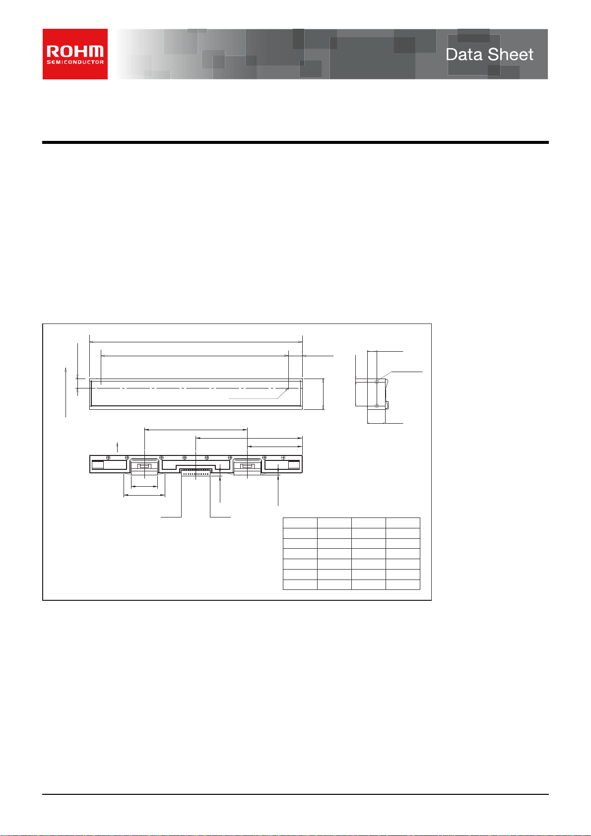
Dimensions (Unit : mm)
5.5±0.5
Paper Feed Direction
(NOTE 1)
(NOTE 2)
A
Deflection at the top of glass:0-0.25
Projection to platen is positive.
Socket Housing:IL-Z-12S-S125C3(JAE)
Socket Contact:IL-Z-C3-A-15000(JAE)
124.0±0.3
109.6(Effective Reading Width:107.8)
60±0.3
15.5±1
25±1
No.12
MAX2
No.1
No.8 Pixel
62±0.3
32±0.3
MAX1.5
Pin No.
No.1
No.2
No.3
No.4
No.5
No.6
8.0±0.5
18.0±0.4
Signal
Ao
GND
VDD
NC
GND
SP
2±0.2
14±0.2
Pin No.
No.7
No.8
No.9
No.10
No.11
No.12
5.6±0.2
2×2-φ2.2
(Depth 5)
10.5±0.4
Signal
GND
CLK
VLED
GLED
RLED
BLED
www.rohm.com
1/4
c
○
2011 ROHM Co., Ltd. All rights reserved.
2011.03 - Rev.B
Characteristics
Parameter
Effective scanning width
Primary scan dot density
Total dot number
Power supply voltage
Scanning speed
Clock frequency
Maximum dynamic range
Minimum dynamic range
Dark output
Operating temperature
∗ Analog signals are produced output at double rate of clock frequency.
Pin assignments
No.
Circuit
1
2
3
4
5
6
7
8ICLK
11
GND
V
GND
GND
RLED
Ao
DD
NC
SP
I / O
O
I
I
−
I
I
I
I
Functions
Analog Output
Ground
Power Supply
Non connect
Ground
Start pulse
Ground
Clock
LED power supply9IVLED
LED ground10 IGLED
LED ground
LED ground12 IBLED
Symbol Typ. Unit
−
−
−
V
DD
SLT
CLK
VRMax.
VRMin.
Vod
−
107.8
200
864
3.3
0.125x3
8
0.5
0.25
0.8±0.2
5 to 45
mm
dpi
dots
V
ms / line
MHz
V
V
V
°C
Data Sheet LSH2004-AA30A
∗
www.rohm.com
2/4
c
○
2011 ROHM Co., Ltd. All rights reserved.
2011.03 - Rev.B

1/fCLK
C
S
A
N
l.
Timing chart
(a) CLK Timing Chart
LK
Data Sheet LSH2004-AA30A
twCLK twCLK
50%50% 50% 50%
50% 50%
P
tSETUP
o
tHOLD
1pixel 2pixel
ts
(b) Data Output Timing Chart
After turning on the SP pulse, the analog output shape starts from the setting up point of 65 clock pulse.
1 2 64 65 66
CLK
SP
Ao
V
REF
Output Period (64pixels) Analog Output Period
1 to 64clock 1 to 864pixels
ote) Output blank part cannot be used as the analog output standard leve
www.rohm.com
3/4
c
○
2011 ROHM Co., Ltd. All rights reserved.
2011.03 - Rev.B

G
B
G
R
Inner circuit
VDD
1μF x 4
ND
Data Sheet LSH2004-AA30A
1
864
680Ω
1μF
SP
CLK
Ao
100kΩ
VLED
GND
GND
GND
Peripheral circuit
12 10 11 9 1 3 6
1μF
ANALOG MEMORY CIRCUIT
8 2 5 7
C5
DD
V
V
REF
220Ω
R1R2
GNDVLEDLED
BGR
C3
C4
GND
C1
V
DD
SP CLK
C2
A
∗ R1=R2=100Ω
C1=47μF
C3=100μF, C4=0.1μF, C5=100pF
∗ Please adjust the value of resistance to fit your interface circuit.
www.rohm.com
4/4
c
○
2011 ROHM Co., Ltd. All rights reserved.
2011.03 - Rev.B

Notes
Notice
www.rohm.com
© 2011 ROHM Co., Ltd. All rights reserved.
Thank you for your accessing to ROHM product informations.
More detail product informations and catalogs are available, please contact us.
ROHM Customer Support System
http://www.rohm.com/contact/
R1120A
 Loading...